Minimizing Standby Power by Optimizing Passive Components · Minimizing Standby Power by Optimizing...
12
Fairchild Semiconductor Power Seminar 2010-2011 1 Minimizing Standby Power by Optimizing Passive Components Young-Bae Park and Sang-Cheol Moon Abstract - The environmental impact of energy consumed by electrical appliances when not in use has attracted growing attention in the international community. This paper discusses how the selection of passive components in switched-mode power supplies (SMPSs) affects standby power consumption. Based on analysis, this paper presents how to select passive components to minimize the standby power consumption of SMPSs. The validity of the proposed selection guideline is verified with a 50W prototype power supply. I. INTRODUCTION Even though most domestic appliances and office equipment are plugged directly into wall outlets and powered from high-voltage alternating current (AC), nearly all of their internal circuitry requires low-voltage direct current (DC). Accordingly, power supplies are required to convert AC voltage to low DC voltage. According to research by Ecos Consulting, roughly 3 billion AC/DC power supplies are used in the United States and about 10 billion globally [1][2] . As they become pervasive, the environmental impact of the energy efficiency of the power supply has attracted growing attention in the international community. As a first step, a number of efforts have improved efficiency when the power supply is in standby mode [3]-[6] . In general, standby mode is when electronic devices wait in low load, expecting an external wake-up signal. This wake-up signal can be activated through a remote control, network connection, keyboard, or mouse. Recently, standby mode has become widely adopted for many applications as users require devices that are always available and can be remotely turned on and off. Electronic devices in standby mode are always on and consume energy required to supply the micro- controller and other standby circuitry. Most electronic appliances such as TVs, personal computers, and monitors, are in standby mode much longer than normal operation mode. As a result, standby power consumption has become a growing concern. According to a report from Lawrence Berkley National Laboratory shown in Table 1, the standby power in developed countries accounts for as much as 10% of national residential electricity use [1][2] . This results in significant carbon dioxide emissions. Governmental and standardization organizations around the world, such as International Energy Agency (IEA) and Environmental Protection Agency (EPA), have endorsed measures to encourage adoption of energy-efficient power supplies. TABLE 1. RESIDENTIAL POWER CONSUMPTION Country Average Resid. Standby Power (W avg ) Annual Elec. Use (kWh/yr) Fraction of Total Resid. Elec. Use Australia 60 527 13% France 38 235 7% Germany 44 389 10% Japan 60 530 12% Netherlands 37 330 10% New Zealand 100 880 11% USA 50 440 5% To date, most of the research to minimize the standby power consumption has been done on reducing the operating current of the PWM controller and improving switching techniques, such as burst switching. Meanwhile, the impact of passive components on standby power consumption has been mostly ignored. This paper discusses how the selection of passive components in switched- mode power supplies (SMPS) affects the standby power consumption. Based on analysis, this paper presents how to select passive components to minimize the standby power consumption of a SMPS, covering the input filter, clamp, dummy load, capacitors, feedback loop, and transformer. Experimental comparison is also presented to show the validity of analysis. Fig. 1 shows a simplified schematic of a flyback converter using a Fairchild Power Switch, or FPS™. This will be used as a reference circuit for the discussion of the passive components.
Transcript of Minimizing Standby Power by Optimizing Passive Components · Minimizing Standby Power by Optimizing...

Fairchild Semiconductor Power Seminar 2010-2011 1
Minimizing Standby Power by Optimizing Passive Components
Young-Bae Park and Sang-Cheol Moon
Abstract - The environmental impact of energy consumed by electrical appliances when not in use has attracted growing attention in the international community. This paper discusses how the selection of passive components in switched-mode power supplies (SMPSs) affects standby power consumption. Based on analysis, this paper presents how to select passive components to minimize the standby power consumption of SMPSs. The validity of the proposed selection guideline is verified with a 50W prototype power supply.
I. INTRODUCTION Even though most domestic appliances and office
equipment are plugged directly into wall outlets and powered from high-voltage alternating current (AC), nearly all of their internal circuitry requires low-voltage direct current (DC). Accordingly, power supplies are required to convert AC voltage to low DC voltage. According to research by Ecos Consulting, roughly 3 billion AC/DC power supplies are used in the United States and about 10 billion globally[1][2]. As they become pervasive, the environmental impact of the energy efficiency of the power supply has attracted growing attention in the international community. As a first step, a number of efforts have improved efficiency when the power supply is in standby mode[3]-[6].
In general, standby mode is when electronic devices wait in low load, expecting an external wake-up signal. This wake-up signal can be activated through a remote control, network connection, keyboard, or mouse. Recently, standby mode has become widely adopted for many applications as users require devices that are always available and can be remotely turned on and off. Electronic devices in standby mode are always on and consume energy required to supply the micro-controller and other standby circuitry.
Most electronic appliances such as TVs, personal computers, and monitors, are in standby mode much longer than normal operation mode. As a result, standby power consumption has become a growing concern. According to a report from Lawrence
Berkley National Laboratory shown in Table 1, the standby power in developed countries accounts for as much as 10% of national residential electricity use[1][2]. This results in significant carbon dioxide emissions. Governmental and standardization organizations around the world, such as International Energy Agency (IEA) and Environmental Protection Agency (EPA), have endorsed measures to encourage adoption of energy-efficient power supplies.
TABLE 1. RESIDENTIAL POWER CONSUMPTION
Country Average Resid. Standby Power
(Wavg)
Annual Elec. Use (kWh/yr)
Fraction of Total Resid.
Elec. Use Australia 60 527 13% France 38 235 7%
Germany 44 389 10% Japan 60 530 12%
Netherlands 37 330 10% New Zealand 100 880 11%
USA 50 440 5%
To date, most of the research to minimize the standby power consumption has been done on reducing the operating current of the PWM controller and improving switching techniques, such as burst switching. Meanwhile, the impact of passive components on standby power consumption has been mostly ignored. This paper discusses how the selection of passive components in switched-mode power supplies (SMPS) affects the standby power consumption. Based on analysis, this paper presents how to select passive components to minimize the standby power consumption of a SMPS, covering the input filter, clamp, dummy load, capacitors, feedback loop, and transformer. Experimental comparison is also presented to show the validity of analysis.
Fig. 1 shows a simplified schematic of a flyback converter using a Fairchild Power Switch, or FPS™. This will be used as a reference circuit for the discussion of the passive components.

Fairchild Semiconductor Power Seminar 2010-2011 2
Fig. 1. Simplified schematic of flyback converter with FPS™.
II. LOSSES RELATED TO PASSIVE COMPONENTS
A. Discharge Resistor at Input Filter
Typically, the line filter of the SMPS is composed of capacitors and a common-mode coupled inductor, as shown in Fig. 1. For safety, it is required that the energy stored in the line filter be discharged naturally once the SMPS is unplugged from the power outlet.
A common method is to place a discharge resistor across the line filter capacitor, which unfortunately causes power consumption as long as the SMPS is connected to the grid.
The discharge resistor should be determined by the trade-off between discharge time and power consumption since these are determined by the value of the resistor, calculated as:
2line
LOSSV
PR
= (1)
ER Cτ = ⋅ (2) where Vline is the line voltage in RMS and CE is the effective capacitance across the input terminal.
Adequate discharge time must be guaranteed to ensure the voltage across the capacitor is lower than the safe level to the human body.
Balance must be achieved between discharge time and power loss. Some exemplary calculations are listed in Table 2. The required time constant is controlled by safety regulations (e.g. UL60950). Using one second as a reference, the first choice of 1.17MΩ resistors in series is undesirable in regards to power loss because it consumes more than 27mW compared to the 3MΩ option, which has a discharge time that meets the reference time.
TABLE 2. POWER LOSS AND DISCHARGE TIME R
DISCHARGE
PLOSS @230VAC τ @C=322nF Remark
1.17MΩ 45.2mW 0.377s 2MΩ 26.5mW 0.644s ∆18.7mW 3MΩ 17.6mW 0.966s ∆27.6mW

Fairchild Semiconductor Power Seminar 2010-2011 3
Reducing capacitance is another approach to
increasing the discharge resistor without increasing the discharge time. EMI reduction techniques like frequency jittering, optimizing gate turn-on speed, and optimizing clamp, can make the input filter smaller. Raising inductance at the input filter can be an alternative, maintaining the same filtering effect while reducing capacitance. However, increasing inductance is not always possible because the physical size of the raised inductor can be limited by the board’s height or using a non-standard inductor may raise the cost. Optimizing the discharge resistor for power loss and discharge time is the first step to decreasing standby power.
B. DC Clamp
A RCD clamp circuit is widely used for flyback converters in the field due to it’s simplicity and low cost. Designing a RCD clamp circuit is explained in several Fairchild application notes[7][8]. From AN-4147[8], the power loss in the RCD clamp circuit is calculated as:
swoCL
CL2peaklksw
SpeakCL
CLLOSS f
nVVV
iL21f
2ti
VP ⋅−
⋅⋅⋅=⋅⋅
⋅= (3)
where: VCL = voltage across the clamp capacitor ipeak = peak current of primary current ts = time for clamp diode turn on fsw = switching frequency Llk = leakage inductance of the transformer nVo = reflected output by turn ratio of transformer
From Equation (3), VCL and fSW emerge as critical and correctable factors to reduce clamp power loss. Additional factors are related to other design criteria such as maximum duty, voltage stress, and dimensional constraints of the transformer.
In Equation (3), it is assumed that the clamp voltage, VCL, is not changing during the switching period due to a relatively large clamp capacitor. During burst operation at light load, however, this assumption is no longer true, as shown in Fig. 2. At light load, switching losses are more dominant as
compared to conduction losses, so reducing switching count is the easiest and most-effective solution for the controller side to reduce standby power. Fairchild uses burst operation for this purpose. Burst operation consists of repetitive, short periods of high frequency switching which begin and end according to the feedback signal as shown in Fig. 2.
Fig. 2. Burst operation of FPS™ switch
The repeat period is called a “burst” period and
the inverse is a burst frequency. The effective switching frequency during burst operation is determined by the multiplication of a burst frequency and switching counts at one burst period. It depends on the feedback loop response and load condition, ranging from several hundred hertz to several kilohertz. In the loss calculation in this paper, 500Hz is used as an effective switching frequency during standby mode. Normal switching frequency is much higher.
During the non-switching period of burst mode, the clamp capacitor voltage is almost discharged through a resistor before the next burst switching starts. Because the capacitor voltage in the RC clamp circuit is zero, the stored energy in the magnetizing inductance should first charge the clamp capacitor before conducting to the secondary side. As a result, more clamp capacitor loss is added to Equation (3) at the burst frequency, not the effective switching frequency. Equation (4) calculates that loss:

Fairchild Semiconductor Power Seminar 2010-2011 4
( ) burst_sw2
CLCLCLLOSS fVC
21P ⋅⋅⋅= (4)
Fig. 3. Clamp circuit power-loss calculation.
Fig. 3 shows the calculated clamp power losses
assuming that Llk is 10µH, ipeak is 0.5A, and nVo is 65V.
To reduce the loss calculated in Equation (4), a Transient Voltage Suppressor (TVS) can be used instead of an RC clamp circuit, as shown in Fig. 4.
Fig. 4. Clamp circuit variations.
The typical junction capacitor of a TVS is several
pF and is much smaller than that of the capacitor used in the RC clamp circuit. The capacitive loss due to the burst operation when TVS is used is negligible.
Unlike the resistance and capacitor, a TVS can accept higher voltages across the clamp circuit due to the energy restoration characteristic. This is helpful in reducing the clamp losses described in Equation (3) by raising the clamp voltage, VCL. However, a voltage spike using a TVS is more noisy than the RC type in Fig. 5 and a TVS itself is considered less reliable by field engineers. Using a TVS should be determined by the trade-offs between standby power consumption and reliable operation.
Fig. 5. Voltage stress of clamp circuits, RC (51kΩ, 3.3nF) clamp (upper),
and 180V TVS (lower).
C. Auxiliary Winding Circuit for Self Biasing
In Fig. 1, supply voltage for the PWM controller is composed of an auxiliary winding, one diode, and one capacitor. It looks simple at first glance, but in reality it is a little more complex.
In a flyback converter, once the secondary reference output winding turns are selected, the other output’s winding turns are chosen proportional to the reference output turns. Voltage from the auxiliary winding is proportional to the secondary DC voltage and can be treated as an additional secondary voltage even though ground is connected to the primary side.
Until recently, the power consumption of the auxiliary power was largely ignored because it was too small compared to the output load. However, to meet tighter standby power regulations, semiconductor makers began to look at the power consumption in the auxiliary circuit. Before going to the semiconductor level, the reverse recovery characteristic of the diode is worth considering.
t [5µs/div]
VDS [100V/div]
VCL [20V/div]
VDS [100V/div]
VCL [20V/div]
Magnetizing energy is consumed.
t [5µs/div]0
4
8
12
16
20
24
0.2 0.3 0.4 0.5 0.6 0.7 0.8 0.9 1.0
P L OS S [mW ]
fSW [kHz]
VCL=70V VCL=90V VCL=70V+burst_lossVCL=90V+burst_loss
P LO
SS[m
W]
Fairchild Semiconductor Power Seminar 2010-2011 5
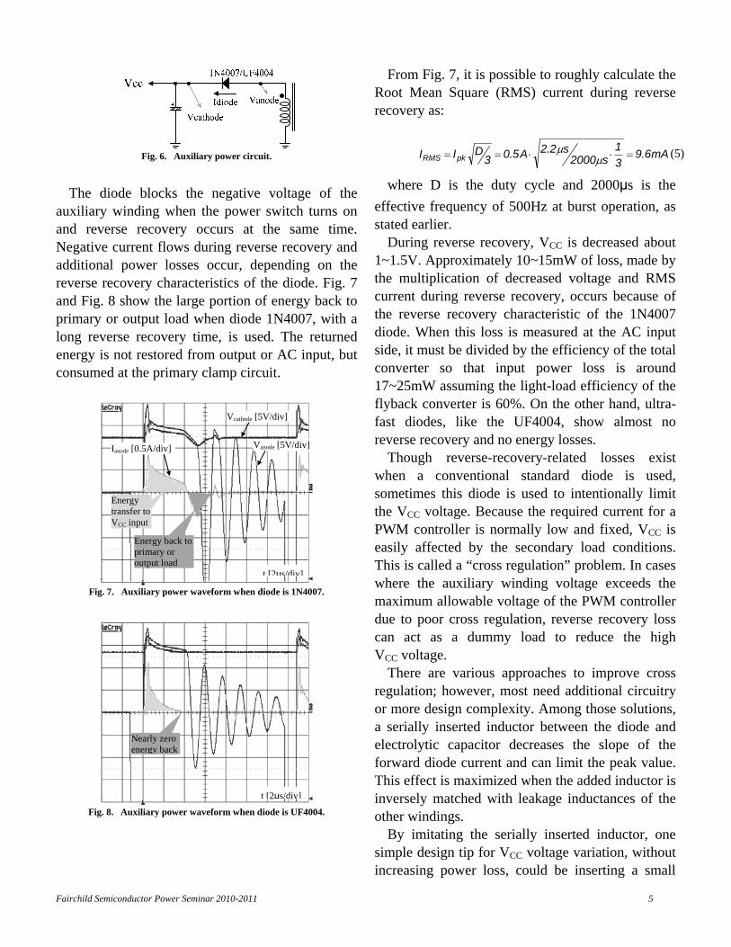
Fig. 6. Auxiliary power circuit.
The diode blocks the negative voltage of the
auxiliary winding when the power switch turns on and reverse recovery occurs at the same time. Negative current flows during reverse recovery and additional power losses occur, depending on the reverse recovery characteristics of the diode. Fig. 7 and Fig. 8 show the large portion of energy back to primary or output load when diode 1N4007, with a long reverse recovery time, is used. The returned energy is not restored from output or AC input, but consumed at the primary clamp circuit.
Fig. 7. Auxiliary power waveform when diode is 1N4007.
Fig. 8. Auxiliary power waveform when diode is UF4004.
From Fig. 7, it is possible to roughly calculate the Root Mean Square (RMS) current during reverse recovery as:
mA6.931
s2000s2.2A5.03
DII pkRMS =⋅⋅== µµ (5)
where D is the duty cycle and 2000µs is the effective frequency of 500Hz at burst operation, as stated earlier.
During reverse recovery, VCC is decreased about 1~1.5V. Approximately 10~15mW of loss, made by the multiplication of decreased voltage and RMS current during reverse recovery, occurs because of the reverse recovery characteristic of the 1N4007 diode. When this loss is measured at the AC input side, it must be divided by the efficiency of the total converter so that input power loss is around 17~25mW assuming the light-load efficiency of the flyback converter is 60%. On the other hand, ultra-fast diodes, like the UF4004, show almost no reverse recovery and no energy losses.
Though reverse-recovery-related losses exist when a conventional standard diode is used, sometimes this diode is used to intentionally limit the VCC voltage. Because the required current for a PWM controller is normally low and fixed, VCC is easily affected by the secondary load conditions. This is called a “cross regulation” problem. In cases where the auxiliary winding voltage exceeds the maximum allowable voltage of the PWM controller due to poor cross regulation, reverse recovery loss can act as a dummy load to reduce the high VCC voltage.
There are various approaches to improve cross regulation; however, most need additional circuitry or more design complexity. Among those solutions, a serially inserted inductor between the diode and electrolytic capacitor decreases the slope of the forward diode current and can limit the peak value. This effect is maximized when the added inductor is inversely matched with leakage inductances of the other windings.
By imitating the serially inserted inductor, one simple design tip for VCC voltage variation, without increasing power loss, could be inserting a small
Nearly zero energy back
t [2µs/div]
Energy transfer to VCC input
Energy back to primary or output load
Ianode [0.5A/div]
Vcathode [5V/div]
Vanode [5V/div]
t [2µs/div]

Fairchild Semiconductor Power Seminar 2010-2011 6
inductor, called a bead, and a serial resistor after the diode, as shown in Fig. 9.
Fig. 9. Modified auxiliary power circuit.
By adding a bead and resistor, VCC voltage can be
lowered more than a UF4004 diode alone and the added components consume negligible energy during standby mode, as shown in Fig. 10.
Fig. 10. Auxiliary power waveform with diode UF4004 and additional
components.
D. Electrolytic Capacitors
Electrolytic capacitors are widely used in many electronic products because of high capacitance, high voltage, flexibility in shape, and low cost. On the other hand, they have many drawbacks such as limited lifetime and high impedances at high frequencies.
The equivalent circuit of an electrolytic capacitor is shown in Fig. 11[11][12].
Fig. 11. Equivalent circuit of electrolytic capacitor.
In Fig. 11, ESR is the equivalent series resistance, ESL is the equivalent series inductance by lead and electrode, C is the capacitance. With the dissipation factor (DF, tanδ) in the capacitor datasheet, it is
possible to calculate the ESR. When a capacitor is ideal, the current leads the voltage across the capacitor by 90 degrees. However, the angle between voltage and current in a real capacitor is not exactly 90 degrees and this difference from 90 degrees is the dissipation factor. If the inductance in Fig. 11 is ignored, the dissipation factor and total effective ESR can be calculated as[12]:
ESRfC2C
1ESR
XESRtan
C⋅==≅ π
ωδ (6)
Once ESR is calculated, its power loss can be
calculated as follows:
( ) ESRIP2CAP
RMSCAPLOSS ⋅= (7)
In a flyback converter, the two suitable positions
for an electrolytic capacitor are DC link and output. The charging and discharging frequency of the output capacitor is the same as the switching frequency of the power switch. The DC link capacitor’s operation follows AC line frequency, and therefore, if the same capacitor types are used in both positions, the power loss caused by ESR in the DC link side is much lower than the output side. Furthermore, charging and discharging current in the DC link side is very small at light loads and the ESR loss becomes smaller. This can also be checked by experiment; power losses are not affected by capacitor types on the DC link side.
As described above, the output electrolytic capacitor is more important when reducing power loss caused by ESR. Fig. 12 and Fig. 13 represent the measured impedance and phase using different capacitor types, but the same capacitance of 25V/1000µF made by SAMYOUNG.
A calculated equivalent circuit is depicted with its simulated curves superimposed on the same graph. The measured ESR of the KMG capacitor, introduced as a standard type in the SAMYOUNG capacitors datasheet, is 138.6mΩ, and the NXB capacitor, which is a low-impedance type in datasheet, is 25.0 mΩ. The estimated power loss of the KMG type is higher than the NXB type.
Ianode [0.5A/div] Vanode [5V/div]
t [2µs/div]
VCC [5V/div]
Fairchild Semiconductor Power Seminar 2010-2011 7
Fig. 12. Frequency response of KMG-type capacitor from SAMYOUNG.
Fig. 13. Frequency response of NXB-type capacitor from SAMYOUNG.
Equation (6) anticipates the ESR without
measuring equipment. From the datasheet, the maximum dissipation
factor of the KMG-type capacitor is 0.2 and the NXB-type is 0.14 at 20oC and 120 Hz.
Ωµππ
δ m265F1000Hz1202
2.0fC2
tanESRmaxKMG =
⋅⋅=≅
(8)
Ωµππ
δ m185F1000Hz1202
14.0fC2
tanESRmaxNXB =
⋅⋅=≅
(9)
These results do not exactly match the experimental results, however, the calculated values are guaranteed at the maximum values from the manufacturer, so regard these values as worst case.
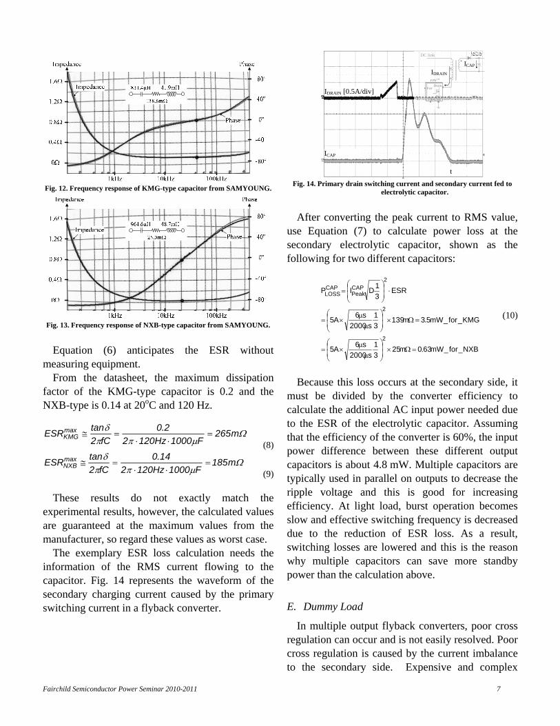
The exemplary ESR loss calculation needs the information of the RMS current flowing to the capacitor. Fig. 14 represents the waveform of the secondary charging current caused by the primary switching current in a flyback converter.
Fig. 14. Primary drain switching current and secondary current fed to
electrolytic capacitor.
After converting the peak current to RMS value,
use Equation (7) to calculate power loss at the secondary electrolytic capacitor, shown as the following for two different capacitors:
NXB_for_mW63.0m2531
s2000s6A5
KMG_for_mW5.3m13931
s2000s6A5
ESR31DIP
2
2
2CAPPeak
CAPLOSS
=Ω×⎟⎟⎠
⎞⎜⎜⎝
⎛
µµ
×=
=Ω×⎟⎟⎠
⎞⎜⎜⎝
⎛
µµ
×=
⋅⎟⎟⎠
⎞⎜⎜⎝
⎛=
(10)
Because this loss occurs at the secondary side, it
must be divided by the converter efficiency to calculate the additional AC input power needed due to the ESR of the electrolytic capacitor. Assuming that the efficiency of the converter is 60%, the input power difference between these different output capacitors is about 4.8 mW. Multiple capacitors are typically used in parallel on outputs to decrease the ripple voltage and this is good for increasing efficiency. At light load, burst operation becomes slow and effective switching frequency is decreased due to the reduction of ESR loss. As a result, switching losses are lowered and this is the reason why multiple capacitors can save more standby power than the calculation above.
E. Dummy Load
In multiple output flyback converters, poor cross regulation can occur and is not easily resolved. Poor cross regulation is caused by the current imbalance to the secondary side. Expensive and complex
t
IDRAIN [0.5A/div]
ICAP
Drain
GNDVcc
FB
FPSTM
Vstr
DC link
IDRAIN
ICAP

Fairchild Semiconductor Power Seminar 2010-2011 8
remedies include post filtering, weighted control, an additional inductor, dummy loads, etc. Among the remedies, the easiest and the least expensive is the introduction of a dummy load.
Fig. 15. Dummy load effect on cross regulation.
Depending on the dummy load, the 14V output
voltage not controlled by the shunt regulator (KA431) is affected (see Fig. 15). According to test results, if one of the components that receives 14V as a power supply cannot accept a 20V maximum power supply input, then adding a 10mA dummy load is the easiest way to limit this voltage below 20V.
Once the dummy load is used, its portion in standby power can be 20~30% of the total input power. Simple smart-circuit correction reduces the dummy load effect on standby power. As shown in Fig. 15, uncontrolled voltage becomes high when the load of the controlled output is heavy. Heavy load does not occur in standby mode. If a dummy load circuit only affects the circuit when the load is heavy, like the right diagram of Fig. 16, then no power loss at standby mode is expected.
Fig. 16. Different dummy load adding.
The dummy load in the right circuit of Fig. 16 consumes no energy when the 14V output is lower than the Zener voltage.
When the 14V output exceeds the Zener voltage, a steeper dummy load variation is needed to create the same effect of a dummy load at the original setting, as shown in Fig. 17. The loss caused by a dummy load on standby power can be almost zero. Other approaches to improve cross regulation are beyond the scope of this paper.
Fig. 17. Power saving due to different dummy load adding.
F. Transformer
Transformer loss can be divided into core loss and copper loss. In addition, the source of copper loss is comprised of DC conduction loss and additional AC losses caused by skin and proximity effects.
When a magnetizing force is applied to the magnetic material, magnetic dipoles are aligned to a certain direction to make the magnetic flux path, and when the magnetizing force is reduced, the magnetic moments relax to the direction of the magnetism. As a result, even an applied magnetizing force returns to zero and the magnetic moments are no longer in a random direction. This is called “magnetic hysteresis” and the source of permanent magnet and core loss.
Copper losses are worsened when considering the proximity effect, which increase the effective RMS current.
When the windings have multiple layers, the current of one layer concentrates on the skin of the wire due to the skin effect and that current induces opposite current in the neighboring second layer
5VOUT
R1
R2
KA431
14.5VOUT
dummy

Fairchild Semiconductor Power Seminar 2010-2011 9
according to Lenz’s law. To cancel the induced current on one surface of the conductor, the same amount of current is induced to the opposite surface of the conductor. At the same time, the neighboring second layer also needs to carry the same current as the first layer. Suppose the current burden of the neighboring second layer is three times that of the first layer. This is known as the proximity effect. According to Ridley[9], the effective AC resistance of the second layer is 3.91 times higher than the DC resistance when the wire thickness is 3mm and the switching frequency is 100 kHz. Therefore, the copper losses can be raised depending on the winding layers.
The best way to build up a transformer to reduce the proximity effect is to use as few winding layers as possible. To avoid core saturation in the flyback transformer, additional turns are needed. The minimum number of turns is a function of inductance Lm, maximum switching current ILIM, designed maximum flux density Bmax, and cross-sectional area of core Ae:
]turns[10AB
ILN 6
emax
LIMMminP ×= (11)
If other factors are the same, except Ae with the
two different cores, it is possible to change the minimum number of turns. With the same volume of cores, some core shapes have bigger Ae values.
Fig. 18. EE core (left) and EER core (right).
As shown in Fig. 18, conventional EER cores
have wider cross sectional area than EE cores. To minimize copper losses, it is better to use
fewer wire turns and layers. However, turns must be higher than the minimum turns. For this, wider Ae values, like EER cores, make it easier to optimize the winding turns and layers.
Fig. 19. Transformer layer of 720µH, primary turns=64(upper) and
700µH, primary turns=43(bottom).
Two cases were compared to see the layer effect
on losses. With the other components exactly same, the input power was reduced to 6mW when the bottom transformer in Fig. 19 was used.
G. Feedback Loop Design
Feedback loop design is not in the scope of this paper and is explained in Fairchild application notes. The resistors R1, R2, RD, and Rbias, not only compensate the feedback signal, but also act as a dummy load.
Fig. 20. Feedback loop circuit.
Using the largest resistors possible is necessary to
minimize power consumption in these resistors. Raising R1 and RD makes compensated DC gain low, which is also combined with CF and RB.
The Current Transfer Ratio (CTR) of the opto-couplers is normally assumed to be 100%. Fairchild’s FOD817 series has various versions from 50% to 600%. If changing from FOD817A, typical CTR is 100%; to FOD817C, typical CTR is

Fairchild Semiconductor Power Seminar 2010-2011 10
300%; RD can be increased without affecting the feedback loop design.
Input power is reduced about 11mW when R1 and R2 are changed from 2kΩ to 8kΩ and the opto coupler is changed from FOD817A to FOD817C.
III. EXPERIMENT To verify the validity of the analysis, a 50W
flyback converter for universal input was prepared. Fig. 23 is the schematic of the tested flyback converter and Table 4 is the bill of materials (BOM).
Based on the analysis of changing the passive components, the resulting power savings are summarized in Fig 21. A reference load of 5V/5mA was used as a comparison because this is the typical load condition during standby mode in leading-edge LCD TVs.
Fig. 21. Summary of experiment test result.
Fig. 22 shows the input power comparison
between the non-optimized SMPS and the optimized SMPS based on the discussion presented in this paper. Power consumption is reduced by more than 100mW. The standby power consumption of the optimized SMPS for other load conditions is shown in Table 3.
0
100
200
300
400
500
600
0 25 50 75 100 125 150 175 200
Inpu
t pow
er [m
W]
Output power [mW]
Non optimized SMPSOptimized SMPS
Fig. 22. Input power difference at various loads and 230VAC.
TABLE 3. RESULTS OF PASSIVE COMPONENTS OPTIMIZED
CONVERTER Load Condition Input Power(mW)
Vo(V) Io(mA) Po(mW) 85VAC 115VAC 230VAC 265VAC 5 0 0 36 36 43 46 5 5 25 67 69 77 80 5 10 50 93 94 102 105 5 15 75 125 127 135 138 5 20 100 156 158 166 171 5 25 125 188 189 198 202 5 30 150 212 215 224 228 5 35 175 245 246 256 261 5 40 200 276 277 287 294
Not all solutions discussed in this paper may be applied due to cost and size limitations of different SMPSs; however, the quantitative awareness of how much power is dissipated in passive components can give insight in to reducing more standby power in PWM controllers as well as passive components.
IV. CONCLUSION This paper discusses how the selection of passive
components in a switched-mode power supply (SMPS) affects standby power consumption. Based on analysis, this paper presents how to select passive components in order to minimize the standby power consumption of SMPSs. The test result from the 50W prototype power supply shows that more than 50% of the standby power consumption can be reduced by the optimum selection of passive components.

Fairchild Semiconductor Power Seminar 2010-2011 11
Fig. 23. Application circuit of experimental converter.
TABLE 4. BILL OF MATERIALS (BOM) OF EXPERIMENTAL CONVERTER
Part Value Note Part Value Note Resistors C301 4.7nF/1kV Ceramic capacitor R102 75kΩ 1/4W, metal film resistor Inductors R201 700Ω 1/4W, metal film resistor L201 5µH 5A rating R202 1.2kΩ 1/4W, metal film resistor L202 5µH 5A rating R203 18kΩ 1/4W, metal film resistor LF201 20mH Line filter R204 8kΩ 1/4W, metal film resistor Diodes
R205 8kΩ 1/4W, metal film resistor D101 P6KE180 180V, 600W peak power transient voltage suppressor, GENERAL SEMI.
Capacitors D102 1N4007 General purpose rectifier, 1A/1000V, FAIRCHILD
C101 150nF/275VAC MKP radial potted capacitor, PILKOR D103 UF4004 Glass passivated high efficiency rectifier, 1A/400V, FAIRCHILD
C102 150nF/275VAC MKP radial potted capacitor, PILKOR D201 MBR20150CT Dual high voltage Schottky barrier rectifier, 20A/150V, FAIRCHILD
C103 100µF/400V Electrolytic capacitor, model=NFA, SAMYOUNG D202 FYPF2006DN Dual Schottky barrier rectifier,
20A/60V, FAIRCHILD C104 33nF/50V Film capacitor BD101 2KBP06M257 Bridge rectifier, 2A/600V, FAIRCHILD
C105 100nF/50V SMD type multi layer ceramic capacitor(MLCC), SEMCO ICs
C106 47µF/50V Electrolytic capacitor, model=NXB, SAMYOUNG IC101 FSGM0565R FPSTM, FAIRCHILD
C201 1000µF/25V Electrolytic capacitor, model=NXB, SAMYOUNG IC102 KA431LZ Programmable shunt regulator,
FAIRCHILD
C202 1000µF/25V Electrolytic capacitor, model=NXB, SAMYOUNG IC103 FOD817C Phototransistor optocoupler,
FAIRCHILD
C203 2200µF/10V Electrolytic capacitor, model=NXB, SAMYOUNG Miscellaneous
C204 2200µF/10V Electrolytic capacitor, model=NXB, SAMYOUNG F101 Fuse 3.15A/250V
C203 47nF/50V Film capacitor NTC101 5D-11 NTC power thermistor, 5Ω 11φ, SAMKYUNG
C206 100nF/50V SMD type multi layer ceramic capacitor(MLCC), SEMCO Trans LM=700µH EER 3019 core
C207 100nF/50V SMD type multi layer ceramic capacitor(MLCC), SEMCO

Fai
[1]
[2]
[3]
[4]
[5]
[6]
[7]
[8]
[9]
[10[11[12[13
irchild Semicondu
VEcos consultingFeb. 2004, preprogram. Chris Calwell, Supply EfficieCompetition OpJ.P. Ross and Power ConsumpAppliances, SepAlan Meier, WElectricity to 1Efficiency in BuYoh Matsushitafax-copier macConscious DesiHangseok ChoConsumption oSpecialist ConfeFairchild AppliFlyback ConverFairchild ApplClamp of FlybaRay Ridley, “PrMagazine, 2005
0] E Cores Datash] Aluminum Elec
2] Capacitor Semi] Robert W. Er
Electronics, 2nd
ctor Power Semin
V. REFEg, “Power Supply epared for the C
Arshad Mansoorency: Key Issuepportunity” APECAlan Meier, “Whption,” Internationptember, 2000.
Wolfgang Huber, a1 Watt,” The 199uildings, August 1a, “Design for lowchine,” Internatioign and Inverse Maoi, D. Y. Huhof SMPS in Stanference, 2005. ication Note AN-rters Using FPS™ication Note AN
ack.” roximity Loss in M5. heet, SAMHWA Elctrolytic Capacitornar Document, SA
rikson, Dragan Md ed., Kluwer Acad
ar 2010-2011
ERENCES Efficiency: Whatalifornia Energy
r, Robert Keefe, “s, Measured Da 2004. hole-House Measnal Conference on
and Karen Rosen98 ACEEE Summ1998. w electric power duonal Symposium anufacturing, pp. 3
h “Techniques tndby Mode,” IEE
-4137, “Design G™.” N-4147, “Design
Magnetics Windin
lectronics. rs Datebook, SAMAMHWA ElectronMaksimovic, Funddemic Publishers, 2
t Have We LearneCommission’s P
“Active Mode Poata and the Des
urements of Stann Energy Efficienc
n, “Reducing Leakmer Study on Ene
uring standby staton Environment
391 – 395, 1999. to Minimize Po
EE Power Electro
Guidelines for Off
Guidelines for R
ngs,” Switching Po
MYOUNG Electronnics. damentals of Po2001.
ed?” IER
ower sign
ndby cy in
king ergy
te of tally
ower nics
fline
RCD
ower
nics.
ower
BLDC mcontrollerfor powereffective
method, correction
YoungelectriUniverrespecsystemhas befor Faas cur
motor controller, r, and so on. He isr electronics for ensolutions.
Sang-engine2005 aKorea (KAISapplicaBucheelectro
design of high-pn (PFC) converters
g-Bae Park rececal engineering rsity, Pusan, Sou
ctively. From 199m engineer in Sameen working as a airchild Semicondurrent feedback act
primary-side-regs interested in ananhancing performa
Cheol Moon receeering from Ajouand the M.S. degr
Advanced InstituST), Daejeon, Koration engineer f
eon, Korea. His ronics; including performance powes.
eived B.S. and Mfrom the Pu
uth Korea, in 1998 and 1999, he
msung electronics asystem and appliuctor. He designetuator controller, hgulated converteralog and digital mance, design simp
eived a B.S. degru University, Suwree in electrical enute of Science area, in 2007. He ifor Fairchild Semresearch interests
analysis, moder converters, and
12
M.S. degrees in usan National 996 and 1998, e worked as a and, since 1999, ication engineer ed systems such hall sensor-less r, novel QRC
mixed controllers licity, and cost-
ree in electrical won, Korea, in ngineering from and Technology is a system and miconductor in s are in power deling, control d power factor