Virtual Memory In Contemporary Microprocessors And 64-Bit Microprocessors Architecture

MICROPROCESSORS 10CS45
CITSTUDENTS.IN
Page 1
Subject Code: 10CS45
Hours/Week : 05
Total Hours : 52
MICROPROCESSORS
(Common to CSE & ISE)
SYLLABUS
I.A. Marks : 25
Exam Hours: 03
Exam Marks: 100
UNIT – 1
PART A [ 7 Hours ]
Introduction, Microprocessor Architecture – 1: A Historical Background, the Microprocessor-
Based
Personal
Computer
Systems.
The
Microprocessor
and
its
Architecture:
Internal
Microprocessor Architecture, Real Mode Memory Addressing.
UNIT – 2 [ 7 Hours ]
Microprocessor Architecture – 2, Addressing Modes: Introduction to Protected Mode Memory
Addressing, Memory Paging, Flat Mode Memory Addressing Modes: Data Addressing Modes,
Program Memory Addressing Modes, Stack Memory Addressing Modes.
UNIT – 3 [ 6 Hours ]
Programming – 1: Data Movement Instructions: MOV Revisited, PUSH/POP, Load-Effective
Address, String Data Transfers, Miscellaneous Data Transfer Instructions, Segment Override
Prefix,
Assembler
Details.
Arithmetic
and
Logic
Instructions:
Addition,
Subtraction
and
Comparison, Multiplication and Division.
UNIT - 4 [ 6 Hours ]
Programming – 2: Arithmetic and Logic Instructions (continued): BCD and ASCII Arithmetic,
Basic Logic Instructions, Shift and Rotate, String Comparisons. Program Control Instructions:
The Jump Group, Controlling the Flow of the Program, Procedures, Introduction to Interrupts,
Machine Control and Miscellaneous Instructions.
PART B
CITSTUDENTS.IN

MICROPROCESSORS 10CS45
CITSTUDENTS.IN
Page 2
UNIT - 5
]
[6 Hours
Programming – 3: Combining Assembly Language with C/C++: Using Assembly Language
with
C/C++
for
16-Bit
DOS
Applications
and
32-Bit
Applications
Modular
Programming,
Using the Keyboard and Video Display, Data Conversions, Example Programs.
UNIT - 6 [7 Hours ]
Hardware
Specifications,
Memory
Interface –
1: Pin-Outs
and
the
Pin
Functions,
Clock
Generator, Bus Buffering and Latching, Bus Timings, Ready and Wait State, Minimum versus
Maximum Mode. Memory Interfacing: Memory Devices
UNIT – 7 [ 6 Hours ]
Memory Interface – 2, I/O Interface – 1: Memory Interfacing (continued): Address Decoding,
8088
Memory
Interface,
8086
Memory
Interface.
Basic
I/O
Interface:
Introduction to
I/O
Interface, I/O Port Address Decoding.
UNIT 8 [7 Hours ]
I/O
Interface – 2,
Interrupts,
and
DMA:
I/O
Interface
(continued):
The
Programmable
Peripheral
Interface
82C55,
Programmable
Interval
Timer
8254.
Interrupts:
Basic
Interrupt
Processing,
Hardware
Interrupts:
INTR
and
INTA/;
Direct
Memory
Access:
Basic
DMA
Operation and Definition.
TEXT BOOK:
1. Barry B Brey: The Intel Microprocessors, 8th Edition, Pearson Education, 2009. (Listed topics only
from the Chapters 1 to 13)
REFERENCE BOOKS:
1. Douglas V. Hall: Microprocessors and Interfacing, Revised Edition, TMH, 2006.
2. K.
Udaya
Kumar &
B.S.
Umashankar :
Advanced
Microprocessors &
IBM-PC
Assembly
Language
Programming, TMH 2003.
3. James L. Antonakos: The Intel Microprocessor Family: Hardware and Software Principles and
Applications, Cengage Learning, 2007.
CITSTUDENTS.IN

MICROPROCESSORS 10CS45
CITSTUDENTS.IN
Page 3
TABLE OF CONTENTS UNIT - 1 Introduction, Microprocessor Architecture-I.
Page No.
1.1 Introduction: A Historical Background
06-32
-1.2 The Microprocessor-Based Personal Computer Systems.
1.3 The Microprocessor and its Architecture
1.4 Internal Microprocessor Architecture
1.5 Real Mode Memory Addressing.
1.6 Real Mode Memory Addressing.
1.7 Introduction to Protected Mode Memory Addressing
UNIT - 2 Microprocessor Architecture – 2, Addressing Modes
2.1 Memory Paging
33-58
2.2 Flat Mode Memory
2.3 Addressing Modes: Data Addressing Modes
2.4
Addressing Modes: continued
2.5 Program Memory Addressing Modes
2.6
Stack Memory Addressing Modes
2.7
Practice of examples
UNIT-3 Programming – 1
3.1 Data Movement Instructions: MOV Revisited, PUSH/POP
59-97
3.2
Load-Effective Address, String Data Transfers,
3.3
Miscellaneous Data Transfer Instructions
3.4 Segment Override Prefix, Assembler Details.
3.5 Arithmetic and Logic Instructions: Addition, Subtraction and Comparison
3.6 Arithmetic and Logic Instructions: Multiplication and Division.
CITSTUDENTS.IN

MICROPROCESSORS 10CS45
CITSTUDENTS.IN
Page 4
UNIT – 4 : Programming – 2:
4.1
Arithmetic and Logic Instructions (continued): BCD
98-116
4.2
ASCII Arithmetic, Basic Logic Instructions
4.3
Shift and Rotate, String Comparisons.
4.4 Program Control Instructions: The Jump Group, Controlling the Flow of the Program
4.5 Procedures, Introduction to Interrupts
4.6
Machine Control and Miscellaneous Instructions.
UNIT – 5 Programming – 3:
5.1 Combining Assembly Language with C/C++
117-123
5.2 Using Assembly Language with C/C++ for 16-Bit DOS Applications
5.3 3 32-Bit Applications Modular Programming,
5.4 Using the Keyboard and Video Display,
5.5 Data Conversions, Example Programs
5.6
Practice of simple examples
UNIT - 6 Hardware Specifications, Memory Interface –1:
6.1
Pin-Outs and the Pin Functions,
124-144
6.2 Clock Generator
6.3 Bus Buffering and Latching
6.4 Bus Timings
6.5
Ready and Wait State
6.6
Minimum versus Maximum Mode.
6.7
Memory Interfacing: Memory Devices
UNIT - 7 Memory Interface –2, I/O Interface – 1:
7.1 Memory Interfacing (continued): Address Decoding 145-159
CITSTUDENTS.IN

MICROPROCESSORS 10CS45
CITSTUDENTS.IN
Page 5
7.2 8088 Memory Interface
7.3 8086 Memory Interface
7.4 Basic I/O Interface: Introduction to I/O Interface
7.5 I/O Port Address Decoding.
7.6 practice
UNIT - 8 I/O Interface – 2, Interrupts, and DMA:
8.1 /O Interface (continued):
160-174
8.2
The Programmable Peripheral Interface 82C55
8.3
Programmable Interval Timer 8254.
8.4 3 Interrupts: Basic Interrupt Processing.
8.5
Hardware Interrupts: INTR and INTA/.
8.6 Direct Memory Access: Basic DMA Operation and
Definition.
8.7 DMA , and practice
CITSTUDENTS.IN

MICROPROCESSORS 10CS45
CITSTUDENTS.IN
Page 6
UNIT 1
INTRODUCTION, MICROPROCESSOR ARCHITECTURE – 1
The internal arrangement of a microprocessor varies depending on the age of the design
and the intended purposes of the processor. The complexity of an integrated circuit is bounded
by physical limitations of the number of transistors that can be put onto one chip, the number of
package terminations that can connect the processor to other parts of the system, the number of
interconnections it is possible to make on the chip, and the heat that the chip can dissipate.
Advancing technology makes more complex and powerful chips feasible to manufacture.
A minimal hypothetical microprocessor might only include an arithmetic logic unit
(ALU) and a control logic section. The ALU performs operations such as addition, subtraction,
and operations such as AND or OR. Each operation of the ALU sets one or more flags in a
status register, which indicate the results of the last operation (zero value, negative number,
overflow. or others). The logic section retrieves instruction operation codes from memory, and
initiates whatever sequence of operations of the ALU required to carry out the instruction. A
single operation code might affect many individual data paths, registers, and other elements of
the processor.
As integrated circuit technology advanced, it was feasible to manufacture more and
more complex processors on a single chip. The size of data objects became larger; allowing
more transistors on a chip allowed word sizes to increase from 4- and 8-bit words up to today's
64-bit words. Additional features were added to the processor architecture; more on-chip
registers speeded up programs, and complex instructions could be used to make more compact
programs.
Floating-point
arithmetic,
for
example,
was
often
not
available on
8-bit
microprocessors, but had to be carried out in software. Integration of the floating point unit first as
a separate integrated circuit and then as part of the same microprocessor chip, speeded up
floating point calculations.
Occasionally the physical limitations of integrated circuits made such practices as a bit
slice approach necessary. Instead of processing all of a long word on one integrated circuit,
multiple circuits in parallel processed subsets of each data word. While this required extra logic
CITSTUDENTS.IN

MICROPROCESSORS 10CS45
CITSTUDENTS.IN
Page 7
to handle, for example, carry and overflow within each slice, the result was a system that could
handle, say, 32-bit words using integrated circuits with a capacity for only 4 bits each.
With the ability to put large numbers of transistors on one chip, it becomes feasible to
integrate memory on the same die as the processor. This CPU cache has the advantage of faster
access
than
off-chip
memory,
and
increases
the
processing
speed
of the
system
for
many
applications.
Generally,
processor
speed
has
increased
more
rapidly
than
external
memory
speed, so cache memory is necessary if the processor is not to be delayed by slower external
memory.
Microprocessor History and Background
The CPU ("central processing unit," synonymous with "microprocessor," or even simply
"processor") is often referred to as the "brain" of the computer.
Choosing the correct processor is vital to the success of your homebuilt computer project.
Here's a little background about the history of microprocessors.
1.1 A Historical Background
In historical background, our aim is to study about the events that led to the
development of microprocessors especially the modern microprocessors, namely, 80x86,
Pentium, Pentium pro, Pentium 3 and the Pentium 4. The historical background can be studied
in three different accounts:
1.The Mechanical Age
2. The Electrical Age
3. The Microprocessor Age
1.1.1 The Mechanical Age: The idea for a system that can compute (calculate) has been
around for a long time, even before the modern electrical and electronic devices came into
existence.
CITSTUDENTS.IN

MICROPROCESSORS 10CS45
CITSTUDENTS.IN
Page 8
ABACUS- the Babylonians invented the abacus sometime during 500 BC. The abacus is the
oldest known mechanical calculator. The working mechanism of abacus is quite simple, it used
strings
of beads
to perform
calculations.
The
abacus
was
not
improved
until
1642
when a
mathematician named
Blaise Pascal
invented
a calculator
that was constructed of
gears
and
wheels. Each gear contained 10 teeth that after one complete revolution advanced a second gear
one place.
The first practical, geared mechanical machines that could automatically compute
information
arrived in
the
1800's.
This
was
much
before
humans
knew
anything
about
electricity or light bulb.(Picture- Abacus).
ANALYTICAL ENGINE- In 1823 The Royal Astronomical Society of
Great Britain commissioned Charles Babbage to produce a programmable calculating machine.
This
machine
was
supposed
to generate
navigational
tables
for
the
Royal
Navy.
Charles
Babbage was aided by Augusta Ada Byron , the countess of Lovelace. Charles Babbage named
this machine 'Analytical Engine'. The Analytical Engine which he conceived had the following
features- it could store 1000 20 digit decimal numbers and a variable program that could
modify the function of this engine. The input to the analytical engine was through punched
CITSTUDENTS.IN

MICROPROCESSORS 10CS45
CITSTUDENTS.IN
Page 9
cards, Charles Babbage borrowed the idea of punched cards from Joseph Jacquard, who used it
to program
the
weaving
machine he
invented in
1801.
After
many
years
of work,
Charles
Babbage realised that it's not possible to make the analytical engine as the machinists of his era
where unable to produce the parts needed for his work. (Picture- Analytical Engine).
1.1.2. The Electrical Age
The Electrical age began with the invention of electric motor by Michael Faraday. With
it came a multitude of motor driven adding machines all based on the mechanical calculator
developed by Blaise Pascal. These electrically driven mechanical calculators where common
office equipment until the early 1970's when small handheld calculators began to appear, first
introduced by Bomar.
In 1889 Herman Hollerith developed a punched card for storing data, he also made a
mechanical
calculator
driven
by the
electric
motors.
His
machine
counted,
sorted
and
collated(to arrange in proper sequence) the data stored in the punched card. The United States
governmnet
commissioned
Herman
Hollerith to
use
his
punched
card
system
to store
and
tabulate information for the 1890 census. In 1896 Herman Hollerith started a company called
the
Tabulating
Machine
Company
which
developed
machines
that
used
punched
cards
for
tabulation. After a number of merges, this Tabulating Machine Company was formed into the
International Business Machines
Corporations now known as
the IBM.
(Picture- Tabulating
machine developed by Herman Hollerith)
The first electronic calculating machine , something which did not require an electric
motor
was
developed
by the
German
Inventor
named
Konrad
Zuse.
His
Z3 calculating
computer where used in aircraft and missile design during World War 2.
CITSTUDENTS.IN

MICROPROCESSORS 10CS45
CITSTUDENTS.IN
Page 10
It has been recently discovered through declassification of British Military documents
that
the
first
electronic
computer
was
put
into
operation in
the
year
1943 to
break
secret
German
Military
codes.
This
electronic
computer
was
invented
by Allan
Turing.
It used
vacuum tubes to perform calculations. He called this electronic computer Colossus. Colossus
was successful in breaking down the secret German military codes generated by the Enigma
machine. The disadvantage with Colossus was that it was not programmable. Colossus was a
fixed program computer system ,which we call today as a special purpose computer.
Konrad Zuse with Z3 computer).
(Picture-
The first general purpose, programmable electronic computer was developed in 1946 at
the University of Pennsylvania. This first modern computer was called the ENIAC (Electronic
Numerical Integrator and Calculator). The ENIAC was a huge machine weighing more than 30
tons and used 17000 vacuum tubes and 500 miles of wires. The ENIAC could perform only
100,000 operations per second. The ENIAC was programmed by rewiring it's circuits. The
ENIAC thrust us into the age of computers. (Picture- ENIAC).
CITSTUDENTS.IN

MICROPROCESSORS 10CS45
CITSTUDENTS.IN
Page 11
1.1.3. The Microprocessor Age
Bell labs developed the transistor in 1948, this was closely followed by the development
of Integrated circuits by Jack Kilby of Texas Instruments in 1958. The integrated circuits led to
the
development
of digital
integrated
circuits in
the
1960's
and
finally
the
development of
microprocessor by Intel Corporation in 1971.
Microprocessor is a programmable controller on a chip. The world's first
microprocessor is the Intel 4004. It was a 4-bit microprocessor that could address only 4096 4-
bit wide memory locations. (Bit is either a 0 or 1 , 4-bit wide memory location can also be
called a nibble). The Intel 4004 instruction set contained only 45 instructions. It was fabricated
with
the
then
current
state of
the
art
P-channel
MOSFET
technology.
Hence
it could
only
execute 50 Kilo instructions per second.
The 4004 microprocessor was readily accepted by the people ,as a result applications
abounded for this device. It was mainly used in early video games and small microprocessor
based applications. The main problems with the early microprocessors where their speed, word
width and memory size. Intel later released the 4040 microprocessor, this was just an update to
the 4004 with improved speed but it did not have any improvement in word width or memory
size.
Other
companies,
particularly
Texas
instruments
also
produced
4-bit
microprocessors
(TMS 1000)
at this time. The 4-bit microprocessors still survives today in low end applications
like microwave ovens and small control systems.
CITSTUDENTS.IN

MICROPROCESSORS 10CS45
CITSTUDENTS.IN
Page 12
In 1971, Intel developed the 8008 microprocessor, an extended 8-bit version of the 4004
microprocessor. This addressed an expanded memory size (16 K bytes) and also had additional
instructions (48 in total) which enabled it's use in more advanced systems. (byte is an 8-bit wide
binary number and K is 1024) .
As engineers
demanded
more
from
8008,
it's
slow
speed ,
small
memory
size
and
instruction set limited it's use. As an welcoming answer to these demands, Intel developed the
8080 microprocessor, the first modern 8-bit microprocessor in 1973. The 8080 addressed an
expanded memory of 64 K bytes which is four times more than the 8008. The 8080 also could
execute instructions 10 times faster than the 8008. An addition instruction which took 20
microseconds(50,000
instructions
per
second) in
8008
took
only 2
microseconds(500,000
instructions per second) in 8080. It also had additional instructions. The 8080 was compatible
with TTL (Transistor-Transistor logic) hence it made it's interfacing easier.
1.2 The Microprocessor Based Personal Computer System
The introduction of microprocessors had a huge impact in the way we use computers.
Computers that once took large areas where reduced to the size of small desktops. Although
these
desktop
computers
are
small
and compact, they possess computing power more than that of the large size computers of the
previous
generation.
Here, in this section, we are going to learn about the structure of a microprocessor based
personal computer system. The block diagram of a personal computer system is shown in the
figure.
This block diagram also applies to any computer system, from the early mainframe computers
to the modern microprocessor based systems. The block diagram consists of three main blocks,
connected to each other with the help of buses. CITSTUDENTS.IN

MICROPROCESSORS 10CS45
CITSTUDENTS.IN
Page 13
Figure 1.1 block diagram of a microprocessor--based computer system. What is a bus? A bus is a series of common connections that carry the same kind of
information. Example- An address bus is a bus with 20 connections that carry the memory
address to the memory.
1.2.1 The memory and the input/output system
The memory structure of all Intel 80x86 to Pentium 4 based personal computer systems are
similar. This includes the first computers based on 8088 introduced in 1981 by IBM to the most
modern computers based on Pentium 4. The memory structure of microprocessor based
computer systems can be divided into three main regions. These are
1. Transient program area (TPA)
2. System area
3. Extended memory system (XMS) CITSTUDENTS.IN

MICROPROCESSORS 10CS45
CITSTUDENTS.IN
Page 14
Figure 1.2 The memory map of a personal computer.
It should be noted that the Extended memory system is not available in those computers
based on 8086 or 8088. In these old computers the TPA and System area exists but not the
Extended memory system. The TPA is of size 640 Kb and System area is of size 384Kb. The
TPA and System area together forms the real or conventional memory which is of size 1024Kb
or 1
Mb.
It's
called as
real
or conventional memory because
each
Intel
microprocessor is
designed to function in this area using its real mode of operation.
Those computer systems that uses the any of the microprocessors, Intel 80286 through Pentium
4, has the 640 Kb of TPA and 384 Kb of system area, In addition , these systems also have an
Extended memory. Hence IBM designates these systems as AT class machines (AT- Advanced
class computer systems). These systems are also called as ISA (Industry standard architecture)
CITSTUDENTS.IN

MICROPROCESSORS 10CS45
CITSTUDENTS.IN
Page 15
or EISA (Extended ISA).
The extended memory available in the computer systems using the 80286- 80386SX
microprocessors is 15Mb. While the amount of extended memory available in the computer
systems using 80386DX
- Pentium microprocessors are 4095Mb, excluding the 1Mb real or
conventional memory. The Computer systems having Pentium pro - Pentium 4 microprocessors
can have 1Mb less than 4Gb to 64GB extended memory. (Note- Modern day computer systems
based on Pentium 4 systems have an extended memory more than 180Gb.)
Recently, a new bus known as the Peripheral Component Interconnect (PCI) bus has been
introduced in the Pentium- Pentium 4 based systems. The older computers based on 8086/8088
used an 8 bit peripheral bus to interface with 8 bit devices. The ISA machines or AT class
machines which used 80286 or above microprocessors used 16 bit peripheral bus for interface.
The EISA machines that used 80386DX and 80486 microprocessors used 32 bit peripheral bus
for interface.
All the new buses were compatible with the
older devices. That is, an 8 bit
interface card is compatible with an 8-bit bus , 16-bit bus or a 32 bit bus. Similarly a 16 bit
interface card is compatible with a 16 bit bus and 32 bit bus.
Another bus type found in the 80486 based computer systems is the VESA local bus or VT bus.
This local bus helps to interface disk and video to the microprocessor. Two new buses have
also
been
introduced,
one is
the
USB or
Universal
Serial
Bus
and
the
other is
the
AGP (
Advanced graphics port)- The Advanced graphics port transfers data between the video card
and the microprocessor at very high speeds.
The Transient Program area (TPA)
The transient program area or TPA holds the DOS operating system and other programs that
control the computer system. The TPA also holds other active or inactive application programs.
We know that the TPA is 640Kb and since it holds DOS on it a part of this 640 Kb is used up
by DOS operating system. The size of the TPA available for other application programs is
628Kb if MS-DOS version 7.X is used as the operating system. The older versions of DOS
used to take up large spaces of TPA leaving only less than 530Kb for other applications.
PC-
DOS is another operating system that is found in computer systems. Both PC-DOS and MS-
DOS are compatible with each other, hence both functioned similarly with application
CITSTUDENTS.IN

MICROPROCESSORS 10CS45
CITSTUDENTS.IN
Page 16
programs. Windows and OS/2 are other operating systems compatible with DOS and allows
DOS programs to execute.
Figure 1.3 The memory map of the TPA in a personal computer.
The memory map of the TPA is shown in the figure. The memory map shows how different
areas of the TPA are allotted to the system programs, data and drivers. To the left of each area
is a hexadecimal number that shows the memory address that begin and end each data area.
1. Interrupt Vectors - The interrupt vectors which occupy the area between 00000 and 00400
is responsible for accessing various features of the DOS, BIOS and other application programs.
2. BIOS communication area and DOS communication area - BIOS is nothing but Basic
Input/Output
System.
BIOS
is a
collection
of programs
that
is stored
in the
ROM or
flash
memory
that
is used to
control
the
Input/Output
devices
that
is connected to
the
computer
CITSTUDENTS.IN

MICROPROCESSORS 10CS45
CITSTUDENTS.IN
Page 17
system. The BIOS and DOS communication areas have transient data that can be used by
programs
to access
the
I/O
devices or
other
parts
of the
computer
system.
3. IO.SYS - The IO.SYS is a program that loads into the TPA from the disk when the computer
system using MSDOS or PCDOS are switched ON. The programs in the IO.SYS enables the
DOS programs to use the keyboard, the display, printer and other I/O devices.
4. MSDOS
- MSDOS
occupies
two
parts
of the
TPA.
One is at
the
top
of TPA
which is
considerably small and 16 bytes in length. The other is at the bottom and is larger. The memory
size occupied by the DOS depends on the version of the DOS installed. Older versions usually
needed larger areas of TPA compared to the newer versions.
5. Device
Drivers-
Drivers
are
those
files
with
an extension
.SYS such as
MOUSE.SYS.
Drivers
are programs that control the installable devices
like mouse,
hand scanner
and
also
other installable application programs. The size of the driver and the number of drivers vary
from
one
computer
to the
another.
6. COMMAND.COM-
The COMMAND.COM helps to control the computer system using
the
keyboard
when
operated
in DOS
mode.
The
COMMAND.COM
program processes
the
DOS
commands
as they
are
typed
from
the
keyboard.
7. Free
TPA-
The
free
TPA
holds
the
active
DOS
application
programs.
These
DOS
application
programs
can
be exemplified as
the
word
processor ,
spreadsheet
and
CAD
programs. In addition to these, free TPA also holds the TSR (Terminate and Stay Resident)
programs. These remain in the free TPA in an inactive state until initiated by a hot-key or an
interrupt.
hotkey.
An example of
TSR
is the
calculator
program
that
is activated
upon
the
ALT+C
SYSTEM AREA
The System area which is smaller than the TPA is considerably important. It contains programs
for data storage and these programs are stored in ROM or flash memory and also in some areas
of the RAM. The system area map is shown in the figure. CIT
STUDENTS.IN

MICROPROCESSORS 10CS45
CITSTUDENTS.IN
Page 18
Figure 1.4The system area of a typical personal computer.
On the left side memory addresses of the particular regions are given in hexadecimal
format. The first area of the system space extends from A0000H to C7FFFH and has the video
display RAM and video control programs. The Video display RAM is stored in two parts, first
from A0000H to A7FFFH and is for the graphical data, second from B0000H to B7FFFH and
stores the text data.
The video BIOS contains programs that control the video display of the
computer and is located on ROM or falsh memory. It's area in system space is from C0000H to
C7FFFH. The size and amount of the memory used depends upon the type of video display
adapter used.
The area C8000H - DFFFFH is free system area and is called the open system area. It is mostly
used as the extended memory system in PC and XT machines ( PC and XT machines means
those computers based on 8086/8088 microprocessor) and as an upper memory system in AT
class machines (Computers using 80286 or above microprocessors).
Memory locations E0000H-EFFFFH contains the cassette BASIC language on ROM found in
CITSTUDENTS.IN

MICROPROCESSORS 10CS45
CITSTUDENTS.IN
Page 19
the older IBM based systems. In almost all the newer systems this particular area is kept open
or free and is also used as RAM to aid the faster operation of DOS application programs.
The system area F0000H to FFFFFH is used
by the System BIOS ROM, but this System BIOS
ROM only operates the I/O devices and is not responsible for the controlling of the video display
system which is done by the separate system BIOS ROM at the location C0000H. The system
BIOS at the top is divided into two parts, first part is in the area F0000H to F7FFFH and
contains programs that set up the computer. The second part contains procedures that control
the I/O devices.
MICROPROCESSOR
Microprocessor can be called as the heart of the microprocessor based personal computer
system. The microprocessor is also known by the names CPU or Central Processing Unit and
controls the working of the computer system.
I/O devices through the buses.
The microprocessor connects to the memory and
The microprocessor follows three simple steps in its working-
1. Transfers data from memory to itself or to the I/O devices.
2. Performs arithmetic and logical calculations.
3. Performs a program via simple decisions.
Even though these processes are simple, the microprocessor is able to solve all types of
problems using this approach. The strength of the microprocessor lies in its ability to execute
millions of instructions per second from the software or programs.
Software and programs are
nothing but a collection of instructions. These software or program is stored in the memory.
This stored program concept makes the microprocessor or in the main, a computer system itself
very
The arithmetic and logical instructions executed by the microprocessor are
efficient.
1. Addition
2. Subtraction
3. Multiplication
4. Division
CITSTUDENTS.IN

MICROPROCESSORS 10CS45
CITSTUDENTS.IN
Page 20
5.
6.
7.
8.
9.
10.
AND
OR
NOT
NEG
Shift
Rotate
Data is stored in the memory or the internal registers. The width of the data is either a byte (8- bits), word (16-bits) or a double word (32-bits). Only the 80386 and above versions are able to execute all three. 8086 to 80286 could directly manipulate 8-bit and 16-bit data but not 32-bit data. A Co-processor called the numeric processor is with the 80486 to aid in arithmetic calculations
dealing with floating point arithmetic. This numerical processor was an in the older 8086- 80386 processors.
additional component
1.3 The Microprocessor and its Architecture: Internal Microprocessor Architecture The Microprocessor Called the CPU (central processing unit).The controlling element in a
computer system. The controlling element in a
through connections called buses.
computer system. Controls memory and
I/O
* buses select an I/O or memory device, transfer data between I/O devices or memory and the
microprocessor
systems
control
I/O
and
memory
systems
microprocessor,
control
I/O
and
memory
* Memory and I/O controlled via instructions stored in memory, executed by the stored in
memory, executed by the microprocessor.
Microprocessor performs three main tasks:
◦ data transfer between itself and the memory or I/O systems
◦ simple arithmetic and logic operations
◦ program flow via simple decisions
Power of the microprocessor is capability to
execute billions of millions of instructions per
second
from a
program
or instructions
per
second
from
a program or
software
(group of
instructions) stored in the memory system.
◦ stored programs make the microprocessor and computer system very powerful devices.
Another powerful feature is the ability to make simple decisions based upon numerical
CITSTUDENTS.IN

MICROPROCESSORS 10CS45
CITSTUDENTS.IN
Page 21
◦ a microprocessor can decide if a number is zero, positive and so forth positive, and so forth
These decisions allow the microprocessor to modify the program flow so programs to modify
the program flow, so programs appear to think through these simple decisions.
The block diagram of 8086 CPU architecture is shown in the figure.
Data registers-
Figure 1.5 8086 CPU Architecture
The registers AX, BX, CX and DX are called as the data registers. They are 16
bits wide and can store both the operands and the results. Each of the data registers can either
be accessed
as a
whole
or the
higher
byte
and
the
lower
byte
can be
accessed separately.
Example- The whole 16 bits in the register AX can be used together or the higher byte and
lower byte can be accessed separately as AH and AL. The registers BX, CX and DX also are
used in other functions in addition as being used as the arithmetic registers.
BX is
CX is
used
used
as a
as an
base
implied
register
counter
in address
by some
calculations.
instructions.
DX is used to hold the I/O address during some I/O operations.
CITSTUDENTS.IN

MICROPROCESSORS 10CS45
CITSTUDENTS.IN
Page 22
Pointer and Index registers- The pointer and index group include the SP, BP, SI, DI and IP.
The SP and IP are essentially the stack pointer and instruction pointer. The instruction pointer is
also called as the program counter. The complete stack and instruction address is formed by
adding the contents of the SP and IP with the contents in CS and SS. BP or base pointer is used
to address the beginning of a stack. It is used in combination with other registers and/or with a
displacement. SI and DI are the index registers, they are used in combination with the BX or
BP and/or a displacement. The SP and BP can be used to store the operands but not the IP.
Formation
of Effective
address
(EA)-
The
data
address
formed
by adding
together, a
combination of ,BX or BP register contents, SI or DI register contents and a displacement is
called as
an effective
address
or offset.
Displacement- The word displacement is used to indicate any quantity that is added to the
register
contents
to form
an effective
address.
Segment registers- The segment registers are CS, SS, DS and ES. The registers that are used
for addressing, SP, BP, SI, DI and IP are 16-bits wide and hence the effective address or offset
will be 16 bits wide but
address is 20 bits wide.
the address that is
required on the address bus
called the physical
Figure 1.6 Formation of physical address
Formation of physical address- We have seen that the address required on the address bus is 20
bits wide but a problem persists as the effective address formed is only 16 bits wide. Hence the
formation of the physical address requires the addition of the contents of the effective address
with the contents of any of the segment registers. To generate the extra 4 bits , we have to
CITSTUDENTS.IN

MICROPROCESSORS 10CS45
CITSTUDENTS.IN
Page 23
append four 0 bits to the right most digit of the number in the segment register. Example if CS
= 123A
and IP
= 341B
, the physical
address
formed
by the
addition
of these two
will be
3 4 1 B +
Figure 1.7 overlapping segments
1 2 3 A 0
1 5 7 B B
Overlapping segments- The use of segment registers divides the memory space into
overlapping
segments
with
each
segment
being 64 Kb
wide
and
beginning at
a memory
location
that
is divisible by
16.
Segment address- Contents of a segment register are called as 'segment address'.
Beginning segment address - Segment address multiplied by 16 is known as 'beginning segment
address'.
Advantages of using segment registers.
1. It allows the memory capacity to be 1Mb even though the individual instructions are
only 16 bits wide.
2. It allows the instruction, data and stack portion to be 64Kb wide by facilitating the use
of more than one instruction, data and stack segment.
3. Facilitates the program, data and stack to have separate memory portions.
4. Allows the program and its data to be stored in separate parts of memory while
execution of the program is performed.
8086 PSW
CITSTUDENTS.IN

MICROPROCESSORS 10CS45
CITSTUDENTS.IN
Page 24
The 8086 PSW is 16 bits, but only 9 of its bits are used. Each bit of 8086 PSW is called a flag.
The
flags
are
divided
into
two
groups,
these
are conditional
flags
and
control
flags.
The
conditional flags reflect the condition involving a previous instruction execution. The control
flags controls the functioning of certain instructions.
Conditional Flags
1. SF (Sign flag)- It is equal to MSB of the result. In 2's compliment a 1 in the MSB shows
that the result is a negative number and a 0 in the MSB shows that the result is a non-negative
number. Hence the sign flag is used to determine whether the result is positive or negative.
2. ZF (Zero flag) - 1 in the zero flag shows that the result is zero and a 0 in the zero flag
shows that the result is a non-zero number.
3. PF (Parity flag) - The PF will become 1 if there are even number of one's in the lower 8-
bits of the PSW.
4. CF (Carry flag) - There are two cases here involving addition and subtraction. In
addition a carry out of the MSB causes this flag to be set. In subtraction if the MSB borrows
then this flag is set.
5. AF (Auxillary carry flag)- In addition the carry out of a bit 3 causes this flag to be set.
In subtraction a borrow by bit 3 causes this flah to be set.
6. OF (Overflow flag)- The overflow flag is set when the result is out of range.
More specifically, in addition, if there is a carry into the MSB and the MSB has no carry out
and in addition, if the MSB needs to borrow and there is no borrow from MSB.
Control flags-
Figure 1.8 8086 PSW
CITSTUDENTS.IN

MICROPROCESSORS 10CS45
CITSTUDENTS.IN
Page 25
1. DF (Direction flags)- Used by string manipulation instructions. If clear, the string is
processed from the beginning, starting with the first element with the lower address If set, the
string is processed from the higher address to the lower most address.
2. IF (Interrupt enable flag)- If enabled it helps the CPU to recognize the maskable
interrupt else these interrupts are ignored.
3. TF (Trap flag)- If set a trap is executed after each instruction.
Buses
A common group of wires that interconnect components in a computer, Transfer address, data,
& control
information
between
microprocessor
memory
and
I/O
between
microprocessor,
memory and I/O.
Three buses exist for this transfer of information: address, data, and control.
Figure 1–10 shows how these buses interconnect various system components.
The address bus requests a memory location from the memory or an I/O location from the I/O
from the memory or an I/O location from the I/O devices
◦ if
I/O is
addressed,
the
address
bus
contains
a 16-bit
I/O
address
from
0000H
through
FFFFH.
◦ if memory is addressed
the bus contains a memory ◦ if memory is addressed, the bus contains
a memory address, varying in width by type of microprocessor.
64-bit extensions to Pentium provide 40 address pins allowing up to 1T byte of memory to be
pins, allowing up to 1T byte of memory to be devices.
accessed.
The data bus transfers information between the microprocessor and its memory and I/O address
microprocessor and its memory and I/O address space.
Data transfers vary in size, from 8 bits wide to 64 bits wide in various Intel microprocessors.
◦ 8088 has an 8-bit data bus that transfers 8 bits of data at a time
CITSTUDENTS.IN

MICROPROCESSORS 10CS45
CITSTUDENTS.IN
Page 26
8086 80286 80386SL 80386SX d 80386EX f ◦ 8086, 80286, 80386SL, 80386SX, and
80386EX transfer 16 bits of data 80386DX 80486SX d 80486DX 32 bit
and 80486DX, 32 bits
◦ 80386DX, 80486SX,
◦ Pentium through Core2 microprocessors transfer 64 bits of data bits of data.
Advantage of a wider data bus is speed in applications using wide data.
In all Intel microprocessors family members, memory is numbered by byte. Pentium through
Core2 microprocessors contain a 64-bit-wide data bus.
Control
bus
lines
select
and
cause
memory or
I/O
to perform a
read
or write
operation to
perform
a read
or write
operation.
In most
computer
systems,
there
are
four
control
bus
connections:
MRDC (memory read control)
MWTC (memory write control)
IORC (I/O read control)( )
IOWC (I/O write control).
Over bar indicates the control signal is active low;
over bar indicates the control signal is
active-low;(active when logic zero appears on control line)
The microprocessor reads a memory location by sending the memory an address through the
sending the memory an address through the address bus.
Next, it sends a memory read control signal to cause the memory to read data.
Data read from memory are passed to the microprocessor through the data bus.
Whenever a memory write, I/O write, or I/O read occurs, the same sequence ensues.
1.4 The Programming Model of 8086 • 8086 through Core2 considered program visible.
– registers are used during programming and are specified by the instructions
• Other registers considered to be program invisible.
– not addressable directly during applications programming
• 80286 and above contain program-invisible registers to control and operate protected
memory.
– and other features of the microprocessor
• 80386 through Core2 microprocessors contain full 32-bit internal architectures.
• 8086 through the 80286 are fully upward-compatible to the 80386 through Core2.
CITSTUDENTS.IN
MICROPROCESSORS 10CS45
CITSTUDENTS.IN
Page 27
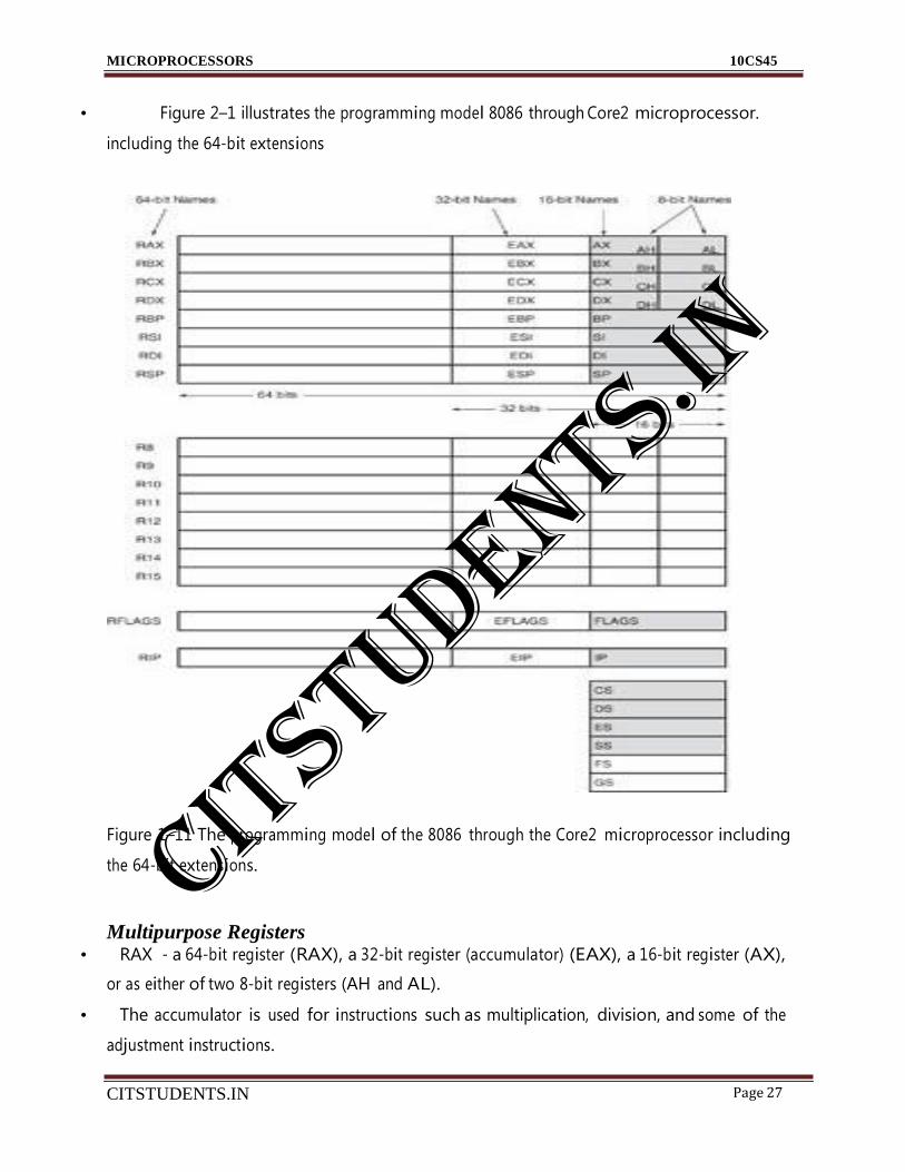
• Figure 2–1 illustrates the programming model 8086 through Core2 microprocessor.
including the 64-bit extensions
Figure 1–11 The programming model of the 8086 through the Core2 microprocessor including
the 64-bit extensions.
Multipurpose Registers • RAX - a 64-bit register (RAX), a 32-bit register (accumulator) (EAX), a 16-bit register (AX),
or as either of two 8-bit registers (AH and AL).
• The accumulator is used for instructions such as multiplication, division, and some of the
adjustment instructions.
CITSTUDENTS.IN
MICROPROCESSORS 10CS45
CITSTUDENTS.IN
Page 28
Intel plans to expand the address bus to 52 bits to address 4P (peta) bytes of memory.
• RBX, addressable as RBX, EBX, BX, BH, BL.
– BX register (base index) sometimes holds offset address of a location in the memory system
in all versions of the microprocessor
• RCX, as RCX, ECX, CX, CH, or CL.
– a (count) general-purpose register that also holds the count for various instructions
• RDX, as RDX, EDX, DX, DH, or DL.
– a (data) general-purpose register
– holds
a part
of the
result
from a
multiplication
or part of dividend before a division
• RBP, as RBP, EBP, or BP.
– points
to a
memory
(base
pointer)
location
for memory data transfers
• RDI addressable as RDI, EDI, or DI.
– often addresses (destination index) string destination data for the string instructions
• RSI used as RSI, ESI, or SI.
– the (source index) register addresses source string data for the string instructions
– like
RDI,
RSI
also
functions
as a
general-
purpose register
• R8 - R15 found in the Pentium 4 and Core2 if 64-bit extensions are enabled.
– data
are
addressed
as 64-,
32-,
16-,
or 8-bit
sizes and are of general purpose
• Most applications will not use these registers until 64-bit processors are common.
– the 8-bit portion is the rightmost 8-bit only
– bits 8
a byte
to 15
are
not
directly
addressable as
Special-Purpose Registers • Include RIP, RSP, and RFLAGS
– segment registers include CS, DS, ES, SS, FS, and GS
• RIP addresses the next instruction in a section of memory.
– defined as (instruction pointer) a code segment
CITSTUDENTS.IN
MICROPROCESSORS 10CS45
CITSTUDENTS.IN
Page 29
• RSP
the stack.
addresses an area of memory called
– the (stack pointer) stores data through this pointer
• RFLAGS indicate the condition of the microprocessor and control its operation.
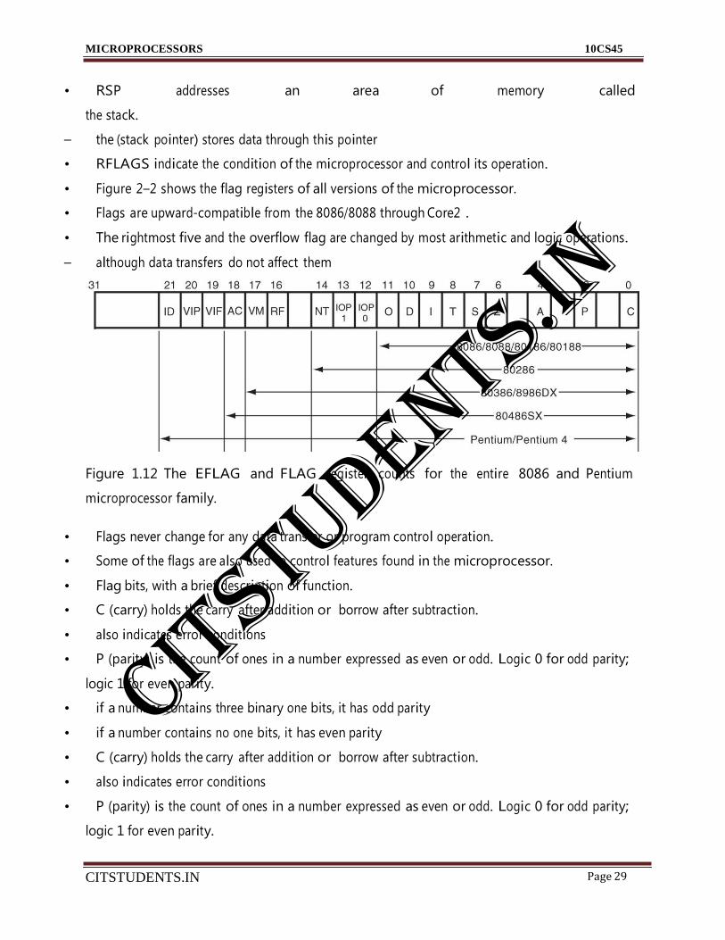
• Figure 2–2 shows the flag registers of all versions of the microprocessor.
• Flags are upward-compatible from the 8086/8088 through Core2 .
• The rightmost five and the overflow flag are changed by most arithmetic and logic operations.
– although data transfers do not affect them
Figure 1.12 The EFLAG and FLAG register counts for the entire 8086 and Pentium
microprocessor family.
• Flags never change for any data transfer or program control operation.
• Some of the flags are also used to control features found in the microprocessor.
• Flag bits, with a brief description of function.
• C (carry) holds the carry after addition or
• also indicates error conditions
borrow after subtraction.
• P (parity) is the count of ones in a number expressed as even or odd. Logic 0 for odd parity;
logic 1 for even parity.
• if a number contains three binary one bits, it has odd parity
• if a number contains no one bits, it has even parity
• C (carry) holds the carry after addition or
• also indicates error conditions
borrow after subtraction.
• P (parity) is the count of ones in a number expressed as even or odd. Logic 0 for odd parity;
logic 1 for even parity.
CITSTUDENTS.IN

MICROPROCESSORS 10CS45
CITSTUDENTS.IN
Page 30
• if a number contains three binary one bits, it has odd parity; If a number contains no one bits,
it
has even parity
• A (auxiliary carry) holds the carry (half-carry) after addition or the borrow after subtraction
between bit positions 3 and 4 of the result.
• Z (zero) shows that the result of an arithmetic or logic operation is zero.
• S (sign) flag holds the arithmetic sign of the result after an arithmetic or logic instruction
executes.
• T (trap) The trap flag enables trapping through an on-chip debugging feature.
• I (interrupt) controls operation of the INTR (interrupt request) input pin.
• D (direction) selects increment or decrement mode for the DI and/or SI registers.
• O (overflow) occurs when signed numbers are added or subtracted.
• an
overflow
indicates
the
result
has
exceeded
the capacity of the machine
• IOPL
used
in protected
mode
operation
to select the privilege level for I/O devices.
• NT (nested task)
mode operation.
flag indicates the current task is nested within another task in protected
• RF (resume)
instruction.
used
with
debugging to
control
resumption of
execution
after
the
next
• VM (virtual mode) flag bit selects virtual mode operation in a protected mode system.
• AC, (alignment check) flag bit activates if a word or doubleword is addressed on a non-word
or non-doubleword boundary.
• VIF is a copy of the interrupt flag bit available to the Pentium 4–(virtual interrupt)
• VIP
(virtual)
provides
information
about
a virtual
mode
interrupt
for
(interrupt
pending)
Pentium.
• used in multitasking environments to provide virtual interrupt flags
• ID (identification)
instruction.
flag
indicates
that
the
Pentium
microprocessors
support
the
CPUID
• CPUID instruction provides the system with information about the Pentium microprocessor
Segment Registers • Generate memory addresses when combined with other registers in the microprocessor.
CITSTUDENTS.IN

MICROPROCESSORS 10CS45
CITSTUDENTS.IN
Page 31
• Four or six segment registers in various versions of the microprocessor.
• A segment register functions differently in real mode than in protected mode.
• Following is a list of each segment register, along with its function in the system.
• CS (code) segment holds code (programs and procedures) used by the microprocessor.
• DS (data) contains most data used by a program.
• Data
address
are
accessed
by an
offset
address or
contents
of other
registers
that
hold
the
offset
• ES (extra) an additional data segment used by some instructions to hold destination data.
• SS (stack) defines the area of memory used for the stack.
• stack entry point is determined by the stack segment and stack pointer registers
• the BP
register
also
addresses
data
within
the stack segment
• FS
and
GS segments
are
supplemental
segment
registers
available in
80386–Core2
microprocessors.
• allow
two
additional
memory
segments
for
access by programs
• Windows
is available.
uses
these
segments
for
internal
operations,
but
no definition
of their
usage
1.4 REAL MODE MEMORY ADDRESSING
Two Real modes of addressing on 80x86
Pentium 4 comes up in the real-mode after it is reset. It will remain in this mode
unless it is switched to protected-mode by software.
• In real mode, the Pentium 4 operates as a very high performance 8086.
• Pentium
4 can
be used
to execute
the
base
instruction
set
of the
8086
MPU
(backward compatibility).
In addition, a number of new instructions (called extended instruction set) have been
added to enhance its performance and functionality (such new instructions can be run in the
real-mode as well as the protected-mode). In real-mode, only the first 1 M bytes of memory
can be addressed with the typical segment:offset logical address. Each segment is 64K bytes
long.
CITSTUDENTS.IN
MICROPROCESSORS 10CS45
CITSTUDENTS.IN
Page 32
• Notice that the Pentium 4 microprocessor has 36 bit address bus, which means it can
support up to 236 = 64G bytes of total memory (which cannot be addressed in real-mode but
can be addressed in protected mode).
• Real mode flat model means
o Strictly converting one address value into a physically meaningful location in the RAM.
• Real mode segmented model means
o
location.
strictly converting two address values into a physically meaningful memory
o gives access to one megabyte (1,048,576 bytes) of directly addressable memory,
known as real mode memory.
a. Segment Registers
• Segment registers are basically memory pointers located inside the CPU.
• Segment registers point to a place in memory where one of the following things begin:
1. Data storage
2. Code execution.
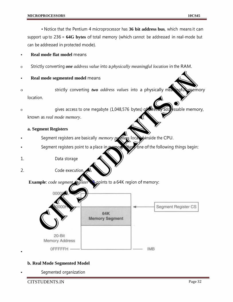
Example: code segment register CS points to a 64K region of memory:
•
b. Real Mode Segmented Model
• Segmented organization
CITSTUDENTS.IN

MICROPROCESSORS 10CS45
CITSTUDENTS.IN
Page 33
o 16-bit wide segments
• Two components
o Base (16 bits)
o Offset (16 bits)
• Two-component specification is called logical address, also called effective address.
• Logical address translates to a 20-bit physical address.
c. Real Mode Segmented Model, Cont.
bits
Addresses are limited to 20 bits:
220
=1,048,576 bytes.
Physical address is generated by adding a
16-bit segment register, shifted left four
plus a 16 bit-offset.
• Generating 20-bit physical address in Real Mode:
d. Problems Related to Segmentation
• Segmentation structures:
often caused grief for programmers who tried to access large data
o Since an offset cannot exceed 16 bits, you cannot increment beyond 64k.
o Instead, program must watch out for a 64k boundary and then play games with the segment register.
• This nightmare was originally created to support CP/M-80 programs ported from 8080 chip to 8086.
CITSTUDENTS.IN

MICROPROCESSORS 10CS45
CITSTUDENTS.IN
Page 34
o
o
9x problems!
Successful short-term thinking;
Catastrophically bad long-term thinking that resulted in never-ending Windows
e. Address Space in Real Mode
Address space in real mode segmented model runs from
o 00000h to 0FFFFFh, within one megabyte of memory.
• For compatibility reasons, Pentium CPU is capable of switching itself into real mode segmented model, is effectively becoming a good old 8086 chip!
CITSTUDENTS.IN

MICROPROCESSORS 10CS45
CITSTUDENTS.IN
Page 35
UNIT-2
2.1 PROTECTED-MODE
• In the protected-mode, memory larger than 1 MB can be accessed.Windows XP operates in
the protected mode.
• In addition, segments can be of variable size (below or above 64 KB).
• Some system control instructions are only valid in the protected mode.
• In
protected
mode,
the
base:offset
logical
memory
addressing
scheme
(which is
used
in real
mode) is changed.
• The
offset
part
of the
logical
memory
address
is still
used. However,
when in
the
protected
mode, the processor can work either with 16-bit offsets (the 16-bit instruction mode) or with 32-
bit
offsets
(the
32-bit
instructionmode). A
32-bit
offset
allows
segments
of up to
4G bytes in
length. Notice
that
in real-mode
the
only
available
instruction
mode
is the
16-bit
mode
(during
which accessing 32-bit registers requires the prefix 66h).
• However,
the
segment
base
address
calculation
is different in
protected
mode.
Instead of
appending a 0 at the end of the segment register contents to create a segment base address (which
gives a 20-bit physical address), the segment register contains a selector that selects a descriptor
from
a descriptor
table.
The
descriptor
describes
the
memory segment's
location,length,
and
access rights. This is similar to selecting one card from a deck of cards in one's pocket.
• Because the segment register and offset address still create a logical memory address, protected
mode
instructions
are
the
same
as real
mode
instructions. In
fact,
most
programs
written to
function in the real mode will function without change in the protected mode.
DESCRIPTORS:
• The selector, located in the segment register, selects one of 8192 descriptors from one of two
tables of
descriptors
(stored
in memory):
the
global
and
local
descriptor
tables. The descriptor
describes the location, length and access rights of the memory segment.
• Each descriptor is 8 bytes long and its format is shown below:
The 8192 descriptor table requires 8 * 8192 = 64K bytes of memory. The
main parts of a descriptor are:
Base (B31 – B0): indicates the starting location (base address) of the memory segment. This
allows segments to begin at any location in the processor's 4G bytes of memory.
CITSTUDENTS.IN

MICROPROCESSORS 10CS45
CITSTUDENTS.IN
Page 36
Limit (L19 – L0): contains the last offset address found in a segment. Since this field is 20 bits,
the
segment
size
could be
anywhere
between 1
and 1M
bytes.
However, if
the
G bit
(granularity
bit)
is set,
the
value
of the
limit is
multiplied
by 4K bytes
(i.e.,
appended
with
FFFH). In this
4K bytes.
case, the segment size could be anywhere between 4K and 4G bytes in
steps of
Example,
Base = Start = 10000000h
Limit = 001FFh and G = 0
So, End = Base + Limit = 10000000h + 001FFh = 100001FFh
Segment Size = 512 bytes
Base = Start = 10000000h
Limit = 001FFh and G = 1
So, End = Base + Limit * 4K = 10000000h + 001FFFFFh = 101FFFFFh
Segment Size = 2M bytes
AV bit: is used by some operating systems to indicate that the segment is available (AV = 1) or
not available (AV = 0).
D bit: If D = 0, the instructions are 16-bit instructions, compatible with the 8086-80286
microprocessors. This means that the instructions use 16-bit offset addresses and 16-bit registers
by default. This mode is the 16-bit instruction mode or DOS mode. If D = 1, the instructions are
32-bits
by default
(Windows XP
works
in this
mode). By
default,
the 32-bit
instruction
mode
assumes
that
all
offset
addresses
and
all
registers
are
32 bits. Note
that
the
default
for
register
size and offset address can be overridden in both the 16- and 32-bit instruction modes using the
66h
and
67h
prefixes. In
16-bit
protected-mode,
descriptors
are
still
used
but
segments
are
supposed to be a maximum of 64K bytes.
Access rights byte: allows complete control over the segment. If the segment is a data segment,
the direction of growth is specified. If the segment grows beyond its limit, the microprocessor's
operating system program is interrupted, indicating a general protection fault. You can specify
CITSTUDENTS.IN

MICROPROCESSORS 10CS45
CITSTUDENTS.IN
Page 37
whether a data segment can be written or is write-protected. The code segment can have reading
inhibited to protect software. This is why It is called protected mode. This kind of protection is
unavailable in realmode.
.
SELECTORS:
Descriptors are chosen from the descriptor table by the segment register.
There are two descriptor tables:
Global
descriptors
table:
contains
segment
definitions
that
apply to
all programs (also called
system descriptors).
Local descriptors table: usually unique to an application (also called application descriptors).
Each descriptor table contains 8192 descriptors, so a total of 16,384 descriptors are available to
an application at any time. This allows up to 16,384 memory segments to be described for each
application. The Figure below shows the segment register in the protected mode. It contains:
13-bit selector field: chooses one of the 8192 descriptors from the descriptor table (213 = 8192).
Table indicator (TI) bit: selects either the global descriptor table (TI = 0) or the local descriptor
table (TI = 1).
Requested privilege level (RPL) field: requests the access privilege level of a memory segment.
The highest privilege level is 00 and the lowest is 11.If the requested privilege level matches or
is higher
in priority
than
the
privilege
level
set by
the
access
rights
byte,
access
is granted.
Windows uses privilege level 00 (ring 0) for the kernel and driver programs and level 11 (ring 3)
for
applications.
Windows
does
not
use
levels 01 or
10. If
privilege
levels
are
violated,
the
system normally indicates a privilege level
violation.
CITSTUDENTS.IN

MICROPROCESSORS 10CS45
CITSTUDENTS.IN
Page 38
Example:
Real Mode: DS = 0008h, then the data segment begins at location 00080h and its length is 64K
bytes.
Protected Mode: DS = 0008h = 0000 0000 0000 1000, then the selector selects Descriptor 1 in
the global descriptor table using a requested privilege level of 00. The global descriptor table is
stored in memory as shown below.
CITSTUDENTS.IN

MICROPROCESSORS 10CS45
CITSTUDENTS.IN
Page 39
Descriptor number 1 contains a descriptor that defines the base address as 00100000h with a
segment limit of 000FFh. This refers to memory locations 00100000h – 001000FFh for the data
segment.
2.2 PROGRAM-INVISIBLE REGISTERS:
The global and local descriptor tables are found in the memory system. In order to specify the
address of these tables, Pentium 4 contains program invisible registers LDTR and GDTR (these
registers are not directly addressed by software).
CITSTUDENTS.IN

MICROPROCESSORS 10CS45
CITSTUDENTS.IN
Page 40
The GDTR (global descriptor table register), LDTR (local descriptor table register) and IDTR
(interrupt descriptor table register) contain the base address of the descriptor table and its limit.
CITSTUDENTS.IN

MICROPROCESSORS 10CS45
CITSTUDENTS.IN
Page 41
The limit of these descriptor tables is 16 bits because the maximum table length is 64K bytes
(but of course, the table could be smaller than 64K byte, hence the need for the limit).
Before using the protected mode, the interrupt descriptor table, global descriptor table along with
the
corresponding
registers
IDTR
and
GDTR
must be
initialized.
This is
why
the
Pentium 4
boots in the real mode not protected mode,
bytes.
and
why the maximum
descriptor
table
size is
64K
Each of the segment registers also contains a program-invisible portion used as a cache to store
the corresponding 8 byte descriptor to avoid repeatedly accessing memory every time the
segment register is referenced (hence the term cache).
These program-invisible registers are loaded with the base address, limit, and access rights each
time the number in the segment register is changed.
The TR (task register) holds a selector, which accesses a descriptor that defines a task. A task is
most often a procedure or application program. The descriptor for the procedure or application
CITSTUDENTS.IN
MICROPROCESSORS 10CS45
CITSTUDENTS.IN
Page 42
program is stored in the global descriptor table, so access can be controlled through the privilege
levels. The task register allows a context or task switch in multitasking systems in about 17s.
Notice: The memory system for the Pentium 4 is 4G bytes in size, but access to the area
between 4G and 64G is enabled with bit position 4 of the control register CR4 and is accessible
only when 4M paging is enabled. When in this paging mode, address lines A35 – A32 are
enabled with a special new addressing mode, controlled by other bits in CR4.
2.3 Memory Paging
Paging is enabled when the PG bit in control register CR0 is set. The paging mechanism can
function in both the real and protected modes.
��When paging is enabled, physical memory is divided into small blocks (typically 4K bytes or
4M bytes) in size, and each block is assigned a page number. The operating system keeps a list
of free pages in its memory. When a program makes a request for memory, the OS allocates a
number of pages to the program.
A key advantage to memory paging is that memory allocated to a program does not have to be
contiguous, and because of that, there is very little internal fragmentation - thus little memory is
wasted.
THE PAGE DIRECTORY AND PAGE TABLE
��To convert a 32-bit linear address into a 32-bit physical address, we need to understand that
the most significant 20 bits of the linear address indicate the linear page number, while the
least significant 12 bits of the linear address indicate the offset within this page. The offset
should remain the same but the linear page number has to be converted into a physical page
number.
CITSTUDENTS.IN

MICROPROCESSORS 10CS45
CITSTUDENTS.IN
Page 43
Each page directory entry is a physical address pointing to a page table, which contains page
table entries. Each page table contains 1024 page table entries, each of which is 4 bytes (32
bits). This means that each page table is 4 K bytes long.
Each page table entry points to the starting physical address of a page in memory (i.e., the
physical page number).
This means that if we have one page directory and 1024 page tables, then we have a total of 1M
table entries or 1 M pages. Since each page is 4K bytes long, this will cover a total of 4G bytes
of maximum physical memory.
The figure below Part (a) shows the linear address (generated by the software) and how it selects
one of the 1024 page directory entries from the page directory (using the left most 10 bits) and
then
selects
one
of the
1024
page
table
entries
(using
the
next
10 bits). Part
(b)
of the
figure
shows the
offset.
page table entry, which contains the physical number that must be associated with the
For
example,
the
linear
addresses
00000000h-00000FFFh
access
the
first
page
directory
entry,
and the first page table entry. Notice that one page
is a
4K-byte address range. So, if that page
table entry contains 00100000h, then the physical address of this page is 00100000h-00100FFFh
for linear address 00000000h-00000FFFh. This means that when the program accesses a location
between
00100000h and
00100FFFh,
the
microprocessor physically
addresses
location
00100000h-00100FFFh.
CITSTUDENTS.IN

MICROPROCESSORS 10CS45
CITSTUDENTS.IN
Page 44
Address
DAPPUW
cw DT
p
C\1.. C\IC\1
C\1 0
Directory Page table Offset
(a)
C\1 6 4 ::> 1 0
- - - -
(b)
Present Writable
User defined Write through Cache disable Accessed
Dirty (0 in page directory)
CITSTUDENTS.IN

MICROPROCESSORS 10CS45
CITSTUDENTS.IN
Page 45
For example, the linear addresses 00000000h-00000FFFh access the first page directory entry,
and the first page table entry. Notice that one page
is a
4K-byte address range. So, if that page
table entry contains 00100000h, then the physical address of this page is 00100000h-00100FFFh
for linear address 00000000h-00000FFFh. This means that when the program accesses a location
between
00100000h and
00100FFFh,
the
microprocessor physically
addresses
location
00100000h-00100FFFh.
The procedure for converting linear addresses into physical addresses:
2.4 8086 Addressing Modes for accessing data CITSTUDENTS.IN

MICROPROCESSORS 10CS45
CITSTUDENTS.IN
Page 46
Addressing modes provide convenience in accessing data needed in an instruction.
8086 Addressing Modes for accessing data
Immediate
Addressing mode
(for source
operand only)
Register addressing Memory addressing I/O port addressing
2.4.1 Immediate Addressing
Before After
Ex1: MOV DX, 1234H DX ABCDH 1234H
Before After
Ex2: MOV CH, 23H CH 4DH 23H CIT
STUDENTS.IN

MICROPROCESSORS 10CS45
CITSTUDENTS.IN
Page 47
2.4.2 Register Addressing
Before After
Ex1: MOV CX, SI CX 1234H 5678H
SI 5678H 5678H
Before After
Ex2: MOV DL, AH Dl 89H BCH
AH BCH BCH
CITSTUDENTS.IN

MICROPROCESSORS 10CS45
CITSTUDENTS.IN
Page 48
Memory Addressing
Direct Addressing Indirect Addressing
Memory Indirect Addressing
Register
Indirect
Based Addressing
with
displacement
Indexed
Addressing with
displacement
Based
Indexed
addressing
Based Indexed
addressing with
displacement
CITSTUDENTS.IN

MICROPROCESSORS 10CS45
CITSTUDENTS.IN
Page 49
2.4.3 Memory Direct Addressing
Before After
Ex1: MOV BX, DS:5634H BX ABCDH 8645H
DS:5634H 45H LS byte
DS:5635H 86H MS byte
Before After
Ex2: MOV CL, DS:5634H CL F2H 45H
DS:5634H 45H
DS:5635H 86H
Ex3: MOV BH, LOC Before After
Program
.DATA
BH C5H 78H
LOC DB 78H
CITSTUDENTS.IN

MICROPROCESSORS 10CS45
CITSTUDENTS.IN
Page 50
2.4.4.Register Indirect Addressing
Before After
Ex1: MOV CL, [SI] CL 20H 78H
SI 3456H
DS:3456H 78H
Before After
Ex2: MOV DX, [BX] DX F232H 3567H
BX A2B2H
DS:A2B2H 67H LS byte
DS:A2B3H 35H MS byte CITSTUDENTS.IN

MICROPROCESSORS 10CS45
CITSTUDENTS.IN
Page 51
Before After
Ex3: MOV AH, [DI] AH 30H 86H
DI 3400H
DS:3400H 86H
Only SI, DI and BX can be used inside [ ] from memory addressing point of view. From user
point of view [BP] is also possible. This scheme provides 3 ways of addressing an operand in
memory.
CITSTUDENTS.IN

MICROPROCESSORS 10CS45
CITSTUDENTS.IN
Page 52
2.4.5 Based Addressing with displacement
Before After
Ex1: MOV DH, 2345H[BX] DH 45H 67H
2345H is 16-bit displacement BX 4000H
4000 + 2345 = 6345H DS:6345H 67H
Before After
Ex2: MOV AX, 45H[BP] AX 1000H CDABH
CITSTUDENTS.IN

MICROPROCESSORS 10CS45
CITSTUDENTS.IN
Page 53
45H is 8-bit displacement BP 3000H
3000 + 45 = 3045H SS:3045H ABH LS byte
It is SS when BP is used SS:3346H CDH MS byte
Base register can only be BX or BP. This scheme provides 4 ways of addressing an operand in
memory.
2.4.6 Indexed Addressing with displacement
Before After
Ex1: MOV CL, 2345H[SI] CL 60H 85H
2345H is 16-bit displacement SI 6000H
6000 + 2345 = 8345H DS:8345H 85H
Before After
Ex2: MOV DX, 37H[DI] DX 7000H B2A2H
CITSTUDENTS.IN

MICROPROCESSORS 10CS45
CITSTUDENTS.IN
Page 54
37H is 8-bit displacement DI 5000H
5000H+ 37H = 5037H DS:5037H A2H LS byte
DS:5038H B2H MS byte
Index register can only be SI or DI. This scheme provides 4 ways of addressing an operand in
memory.
2.4.7Based Indexed Addressing
Before After
Ex1: MOV CL, [SI][BX] CL 40H 67H
SI 2000H
BX 0300H
2000H + 0300H = 2300H DS:2300H 67H
Before After
Ex2: MOV CX, [BP][DI] CX 6000H 6385H
CITSTUDENTS.IN
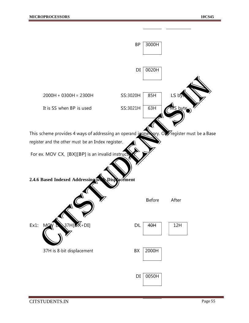
MICROPROCESSORS 10CS45
CITSTUDENTS.IN
Page 55
BP 3000H
DI 0020H
2000H + 0300H = 2300H SS:3020H 85H LS byte
It is SS when BP is used SS:3021H 63H MS byte
This scheme provides 4 ways of addressing an operand in memory. One register must be a Base
register and the other must be an Index register.
For ex. MOV CX, [BX][BP] is an invalid instruction.
2.4.6 Based Indexed Addressing with Displacement
Before After
Ex1: MOV DL, 37H[BX+DI] DL 40H 12H
37H is 8-bit displacement BX 2000H
DI 0050H
CITSTUDENTS.IN
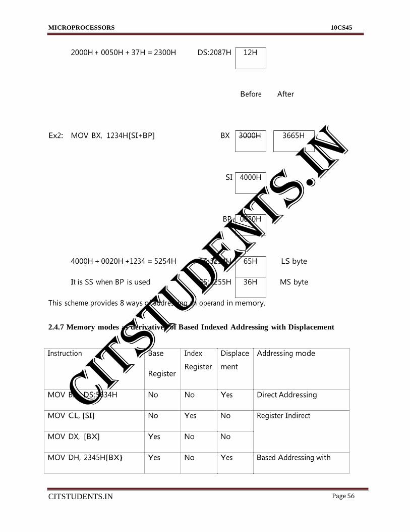
MICROPROCESSORS 10CS45
CITSTUDENTS.IN
Page 56
2000H + 0050H + 37H = 2300H DS:2087H 12H
Before After
Ex2: MOV BX, 1234H[SI+BP] BX 3000H 3665H
SI 4000H
BP 0020H
4000H + 0020H +1234 = 5254H SS:5254H 65H LS byte
It is SS when BP is used SS:5255H 36H MS byte
This scheme provides 8 ways of addressing an operand in memory.
2.4.7 Memory modes as derivatives of Based Indexed Addressing with Displacement
Instruction Base
Register
Index
Register
Displace
ment
Addressing mode
MOV BX, DS:5634H No No Yes Direct Addressing
MOV CL, [SI] No Yes No Register Indirect
MOV DX, [BX] Yes No No
MOV DH, 2345H[BX} Yes No Yes Based Addressing with
CITSTUDENTS.IN

MICROPROCESSORS 10CS45
CITSTUDENTS.IN
Page 57
Displacement
MOV DX, 35H[DI] No Yes Yes Indexed Addressing with
displacement
MOV CL, 37H[SI+BX] Yes Yes No Based Indexed Addressing
MOV DL, 37H[BX+DI] Yes Yes Yes Based Indexed Addressing
with displacement
2.4.8 I/O port Addressing
I/O port Addressing
Fixed port addressing Variable port addressing
Or Direct Port addressing Or Indirect port addressing
Fixed Port Addressing
Before After
Ex. 1: IN AL, 83H AL 34H 78H
Input port no. 83H 78H
CITSTUDENTS.IN

MICROPROCESSORS 10CS45
CITSTUDENTS.IN
Page 58
Before After
Ex. 2: IN AX, 83H AX 5634H F278H
Input port no. 83H 78H
Input port no. 84H F2H
Before
After
Ex. 3: OUT 83H, AL AL 50H
Output port no. 83H 65H 50H
Before
After
Ex. 4: OUT 83H, AX AX 6050H
Output port no. 83H 65H 50H
Output port no. 84H 40H 60H
IN and OUT instructions are allowed to use only AL or AX registers. Port address in the range
00 to FFH is provided in the instruction directly.
2.4.9.Variable Port Addressing
I/O port address is provided in DX register. Port address ranges from 0000 to FFFFH. Data
transfer with AL or AX only.
CITSTUDENTS.IN

MICROPROCESSORS 10CS45
CITSTUDENTS.IN
Page 59
Before After
Ex. 1: IN AL, DX AL 30H 60H
DX 1234H
Input port no. 1234H 60H
Before After
Ex. 2: IN AX, DX AX 3040H 7060H
DX 4000H
Input port no. 4000H 60H
Input port no. 4001H 70H
Before After
Ex. 3: OUT DX, AL AL 65H
DX 5000H
Output port no. 5000H 80H 65H
CITSTUDENTS.IN

MICROPROCESSORS 10CS45
CITSTUDENTS.IN
Page 60
Before After
Ex. 4: OUT DX, AX AX 4567H
DX 5000H
Output port no. 5000H 25H 67H
Output port no. 5001H 36H 45H
CITSTUDENTS.IN

MICROPROCESSORS 10CS45
CITSTUDENTS.IN
Page 61
Unit - 3
3.1 8086 Instruction set
Abbreviations used
R8= AL/BL/CL/DL/ AH/BH/CH/DH
R16=AX/BX/CX/DX/ SI/DI/BP/SP R=R8/R16
SR=CS/DS/ES/SS AR=SI/DI/BX/BP
d16=16-bit data d8=8-bit data
a8=8-bit I/O port address
M8=contents of byte memory
M16=contents of word memory M=M8/M16
Conventions used:
R
MOV for MOV R, M
M
and MOV
M, R
PUSH/POP R16 for PUSH R16 and POP R16 CIT
STUDENTS.IN

MICROPROCESSORS 10CS45
CITSTUDENTS.IN
Page 62
ROR R/M, 1/CL for ROR R,1 ROR M,1 ROR R,CL ROR M, CL
3.1.1 8086 Instruction set types
Instructions are normally discussed under:
Data Transfer instructions Ex. MOV BX, CX
Arithmetic instructions Ex. ADD BX, CX
Logical group of instructions Ex. AND BX, CX
Stack group Ex. PUSH DX I/O group Ex. IN AL, 30H
Branch group Ex. JNC LOCN
String instructions Ex. MOVS
Interrupt instructions Ex. INT 21H
Data Transfer group, Arithmetic group, Logical group, Stack group, and I/O group of
instructions explained first. They occupy several chapters in books.
Here, I explain them under:
2-operand instructions Ex. ADD BX, CX
1-operand instructions Ex. PUSH SI
0-operand instructions: Ex. DAA
Branch group, String instructions, and Interrupt instructions are explained later. CITSTUDENTS.IN

MICROPROCESSORS 10CS45
CITSTUDENTS.IN
Page 63
1234H
1000H
ABCDH
ABCDH
1234H
3.2Operand instructions
3.2.1Operand instructions involving R and R/M
MOV/XCHG Data transfer
ADD/ADC/SUB/SBB R Arithmetic
AND/OR/XOR/TEST/CMP R/M Logical
11 instructions x 210= 11264 opcodes
MOV instruction already discussed- see Instruction template
In data transfer instructions flags are not affected.
3.2.2 Exchange Instruction
Before After
XCHG DX, [BX] DX
BX
DS:1000H
DS:1002H
CITSTUDENTS.IN

MICROPROCESSORS 10CS45
CITSTUDENTS.IN
Page 64
1234H
1000H
2000H
30H
1
2000H
50H
60H
3.2.3 Add instruction
Unlike in 8085, result of add/subtract can be in any register or memory location
Before After
ADD [BX], DX DX
BX
In 3234H, 34H has DS:1000H 3234H
three 1’s. So P flag =0 DS:1002H
Before After
ADC DH ,[SI] DH 81H
Add with Carry Carry flag 0
SI
81H DS:2000H
1000 0001B(Two 1’s) DS:2001H
New flag values: Ac=0, S=1, Z=0, V=1, P=1
Before After
SUB DH, CL DH 30H 0BH
Subtract (without borrow)
CL 25H
0BH =
CITSTUDENTS.IN

MICROPROCESSORS 10CS45
CITSTUDENTS.IN
Page 65
0000 1011B(Three 1’s)
New flag values: Ac=1, S=0, Z=0, V=0, P=0, Cy=0
Before After
SBB DH, CL DH 20H FAH
Subtract (with borrow) Cy flag 1 1
CL 25H
FAH =1111 1010(Six 1’s)
2’s complement of FAH=0000 0110 = +06 So, FAH = -06
New flag values: Ac=1, S=1, Z=0, V=0, P=1, Cy=1
Discussion about Overflow (V) flag V
23H (+ve) 43H (+ve)
+ 46H (+ve) + 54H (+ve)
= 69H (+ve) = 97H (-ve)
V= 0, Cy = 0 V = 1, Cy = 0
Correct answer Wrong answer
Overflow used with signed numbers only
Carry flag used with unsigned numbers only
83H (-ve) F2H (-ve)
+ 94H (-ve) + F3H (-ve)
CITSTUDENTS.IN

MICROPROCESSORS 10CS45
CITSTUDENTS.IN
Page 66
= 17H (+ve) = E5H (-ve)
V= 1, Cy = 1 V = 0, Cy = 1
Wrong answer Correct answer
94H (-ve) F6H (-ve)
- 83H (-ve) - 43H (+ve)
= 11H (+ve) = B3H (-ve)
V= 0, Cy = 0 V = 0, Cy = 0
Correct answer Correct answer
94H (-ve) 66H (+ve)
- 23H (+ve) - 83H (-ve)
= 71H (+ve) = E3H (-ve)
V= 1, Cy = 0 V = 1, Cy = 1
Wrong answer Wrong answer
3.2.4 AND instruction
Before After
AND BH, CL BH 56H 06H
Subtract (with borrow) AND 1 1
0FH=0000 1111B CL 0FH
06H=0000 0110B
CITSTUDENTS.IN

MICROPROCESSORS 10CS45
CITSTUDENTS.IN
Page 67
Use: Selectively reset to 0 some bits of the destination
Bits that are ANDed with 0’s are reset to 0
Bits that are ANDed with 1’s are not changed
3.2.5 OR instruction
Before
After
OR BH, CL BH 56H 5FH
56H=0101 0110B OR
0FH=0000 1111B CL 0FH
5FH=0101 1111B
Use: Selectively set to 1 some bits of the destination
Bits that are ORed with 1’s are set to 1
Bits that are ORed with 0’s are not changed
3.2.6 Ex-OR instruction Before
After
XOR BH, CL BH 56H 59H
56H=0101 0110B XOR
0FH=0000 1111B CL 0FH
59H=0101 1001B
Use: Selectively complement some bits of the destination.
Bits that are XORed with 1’s are complemented
Bits that are XORed with 0’s are not changed
CITSTUDENTS.IN

MICROPROCESSORS 10CS45
CITSTUDENTS.IN
Page 68
3.2.7 TEST instruction
Before
After
TEST BH, CL BH 56H 56H
56H=0101 0110B AND
0FH=0000 1111B CL 0FH 0FH
06H=0000 0110B
Only flages are affected Temp 45H 06H
TEST basically performs AND operation. Result of AND is not stored
in destination. It is
stored in
Temp
register. Temp
is not
accessible to
programmer. There is no instruction like MOV Temp, 67H
3.2.8 Compare Instruction
Before After
CMP BH, CL BH 56H 56H
56H=0101 0110B
0FH=0000 1111B CL 0FH
Only flags are affected
Temp 45H 47H
CMP basically performs Subtract operation. Result of CMP is not
stored in
destination. It
is stored
in Temp
register.
Temp is
not
accessible to programmer. CIT
STUDENTS.IN

MICROPROCESSORS 10CS45
CITSTUDENTS.IN
Page 69
3.3 Operand Instructions involving immediate data
MOV
ADD/ADC/SUB/SBB R/M, d8/d16
AND/OR/XOR/TEST/CMP
8 byte registers + 8 word registers+ 24 byte
memory + 24 word memory = 64 opcodes
10 instructions x 64 = 640 opcodes
3.3.1 Move Immediate data to a Register/ Memory location
Before After
MOV DX, ABCDH DX 1234H ABCDH
Before After
MOV BH, 12H BH 56H 12H
3.3.2 Add Immediate data to a Register/ Memory location
Before After
ADD [BX], 12H BX 1000H
DS:1000H 20H 32H
DS:1001H
CITSTUDENTS.IN

MICROPROCESSORS 10CS45
CITSTUDENTS.IN
Page 70
Before After
ADD [BX], 1234H BX 1000H
DS:1000H 2000H 3234H
DS:1002H
3.3.3 Add with Carry Immediate data to a Register/ Memory location
Before After
ADC DH, 32H DH 30H 63H
Add with Carry Carry flag 1 0
63H= 0110 0011 It has four 1’s
New flag values: Ac=0, S=0, Z=0, V=0, P=1
3.3.4 Subtract Immediate data from a Register/ Memory location
Before After
SUB DH, 40H DH 30H F0H
Subtract (without borrow)
F0H=1111 0000 B(Four 1’s)
New flag values: Ac=0, S=1, Z=0, V=0, P=1, Cy=1
3.3.5 Subtract with borrow Immediate data from a Register/ Memory location
CITSTUDENTS.IN
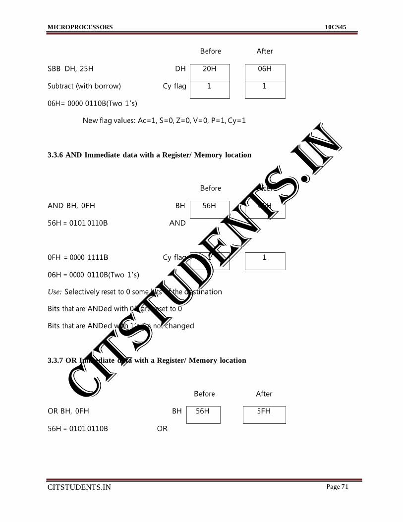
MICROPROCESSORS 10CS45
CITSTUDENTS.IN
Page 71
Before After
SBB DH, 25H DH 20H 06H
Subtract (with borrow) Cy flag 1 1
06H= 0000 0110B(Two 1’s)
New flag values: Ac=1, S=0, Z=0, V=0, P=1, Cy=1
3.3.6 AND Immediate data with a Register/ Memory location
Before After
AND BH, 0FH BH 56H 06H
56H = 0101 0110B AND
0FH = 0000 1111B Cy flag 1 1
06H = 0000 0110B(Two 1’s)
Use: Selectively reset to 0 some bits of the destination
Bits that are ANDed with 0’s are reset to 0
Bits that are ANDed with 1’s are not changed
3.3.7 OR Immediate data with a Register/ Memory location
Before After
OR BH, 0FH BH 56H 5FH
56H = 0101 0110B OR
CITSTUDENTS.IN

MICROPROCESSORS 10CS45
CITSTUDENTS.IN
Page 72
0FH = 0000 1111B CL 0FH
5FH = 0101 1111B
Use: Selectively set to 1 some bits of the destination
Bits that are ORed with 1’s are set to 1
Bits that are ORed with 0’s are not changed
3.3.8 Ex-OR Immediate data with a Register/ Memory location
Before After
XOR BH, 0FH BH 56H 59H
56H = 0101 0110B XOR
0FH = 0000 1111B CL 0FH
59H = 0101 1001B
Use: Selectively complement some bits of the destn.
Bits that are XORed with 1’s are complemented
Bits that are XORed with 0’s are not changed
3.3.9 Test immediate data with a Register/ Memory location
Before After
TEST BH, 0FH BH 56H 56H
56H=0101 0110B AND
0FH=0000 1111B Temp 45H 06H
CITSTUDENTS.IN

MICROPROCESSORS 10CS45
CITSTUDENTS.IN
Page 73
06H=0000 0110B
TEST basically performs AND operation. Result of AND is not stored in
destination. It is stored in Temp register. Temp is not accessible to
programmer. There is no instruction like MOV Temp, 67H. Only flags
are affected.
3.4 Compare immediate data with a Register/ Memory location
Before After
CMP BH, 0FH BH 56H 56H
56H=0101 0110B AND
Temp 45H 47H
CMP basically performs Subtract operation. Result of CMP is not stored in
destination. It is stored in Temp register. Temp is not accessible to
programmer. Only Flags are affected based result of subtraction.
3.4.1 Operand Instructions involving SR and R16/M16
MOV SR
R16/M16
Before After
MOV DS, CX DS 1122H 2233H
CX 2233H
CITSTUDENTS.IN

MICROPROCESSORS 10CS45
CITSTUDENTS.IN
Page 74
Note that there is no instruction to load an immediate data to a Segment
register.
No. of opcodes = 2 x 4 x (8+24) = 256
Before After
MOV DS, [BX] DS 1122H 2233H
BX 2000H
DS:2000H 2233H
3.4.2 Operand Instructions to perform Input operation
IN AL/AX, a8/DX 4 opcodes
Before After
IN AL, DX AL 50H 45H
DX 2111H
Input port no. 2111H 45H
Before After
IN AL, 30H AL
Input port no. 30H
50H
45H
45H CITSTUDENTS.IN

MICROPROCESSORS 10CS45
CITSTUDENTS.IN
Page 75
3050H
1177H
45H
40H
3050H
2177H
45H
40H
Before After
IN AX, DX AX 4045H
DX
Input port no. 60H
Input port no. 61H
3.4.3 Operand Instructions to perform Output operation
OUT a8/DX, AL/AX 4 opcodes
Before After
OUT 30H, AL AL 50H
Out port no. 30H 40H 50H
Before After
OUT DX, AX AX
DX
Out port no. 2177H 50H
Out port no. 2178H 30H
Before After
OUT 60H, AX AX 3050H
CITSTUDENTS.IN

MICROPROCESSORS 10CS45
CITSTUDENTS.IN
Page 76
Out port no. 60H 45H 50H
Out port no. 61H 40H 30H
3.4.4 Operand Instructions to perform Shift/Rotate operation
ROR /ROL /RCR /RCL /SHR /SHL /SAR R/M, 1/CL
7 instructions x (16+48) x 2 = 896 opcodes
SHR and SHL: for shifting left / right unsigned numbers
SAR used Shifting right a signed number
SHL is also called as SAL, as method for shift left of signed or unsigned number is the same
ROR R/M, 1/CL Used for division by power of 2
CL has no. of times rotation is to be done
ROR BH, 1 R/M Cy
Rotate right without cy Before After
BH 0100 0010 0010 0001
Cy 1 0
RCR R/M, 1/CL
CITSTUDENTS.IN

MICROPROCESSORS 10CS45
CITSTUDENTS.IN
Page 77
CL has no. of times rotation is to be done
RCR BH, 1 R/M Cy
Rotate right with cy Before After
BH 0100 0010 1010 0001
Cy 1 0
ROL R/M, 1/CL Used for multiplication by 2n
ROL BH, CL Cy R/M
Rotate left without cy Before After
BH 0010 0010 1000 1000
CL 02H
Cy 1 0 CITSTUDENTS.IN

MICROPROCESSORS 10CS45
CITSTUDENTS.IN
Page 78
RCL R/M, 1/CL
RCL BH, CL Cy R/M
Rotate left with cy Before After
BH 0010 0010 1000 0010
CL 02H
Cy 1 0
SHL R/M, 1/CL Used for multiplication by 2n
SHL BH, CL Cy R/M
0
Shift left without cy Before After
BH 0010 0010 1000 1000
CL 02H
Cy 1 0
SHR R/M, 1/CL Used for division by 2n of unsigned nos
SHR BH, CL R/M Cy
0
CITSTUDENTS.IN
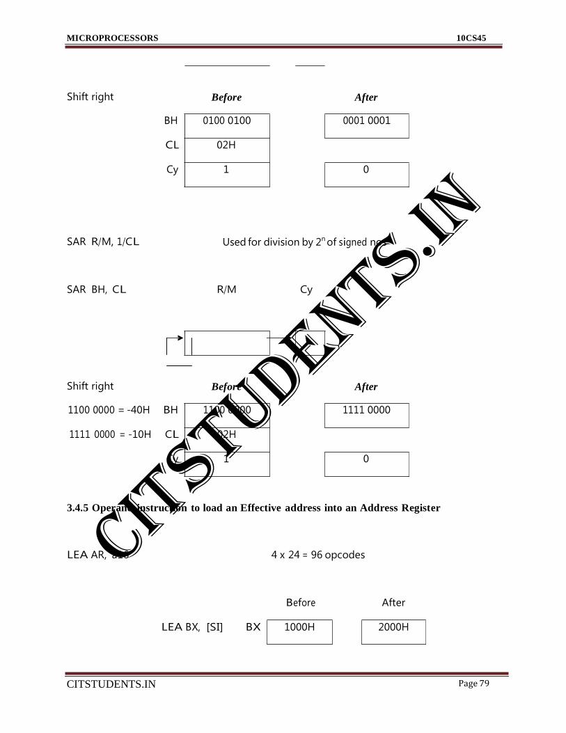
MICROPROCESSORS 10CS45
CITSTUDENTS.IN
Page 79
Shift right Before After
BH 0100 0100 0001 0001
CL 02H
Cy 1 0
SAR R/M, 1/CL Used for division by 2n of signed nos
SAR BH, CL R/M Cy
Shift right Before After
1100 0000 = -40H BH 1100 0000 1111 0000
1111 0000 = -10H CL 02H
Cy 1 0
3.4.5 Operand instruction to load an Effective address into an Address Register
LEA AR, a16 4 x 24 = 96 opcodes
Before After
LEA BX, [SI] BX 1000H 2000H
CITSTUDENTS.IN

MICROPROCESSORS 10CS45
CITSTUDENTS.IN
Page 80
LEA BX, [SI] functionally same as SI 2000H
MOV BX,SI
DS:2000H 3000H
3.4.6 Operand instruction to load DS and an Address Register from memory
LDS AR, M32 4 x 24 = 96 opcodes
Before After
LDS SI, 3000H DS 2000H 7000H
Loads DS and SI using single instruction
SI 1000H 6000H
DS:3000H 6000H
DS:3002H 7000H
3.4.7 Operand instruction to load ES and an Address Register from memory
LES AR, M32 4 x 24 = 96 opcodes
CITSTUDENTS.IN
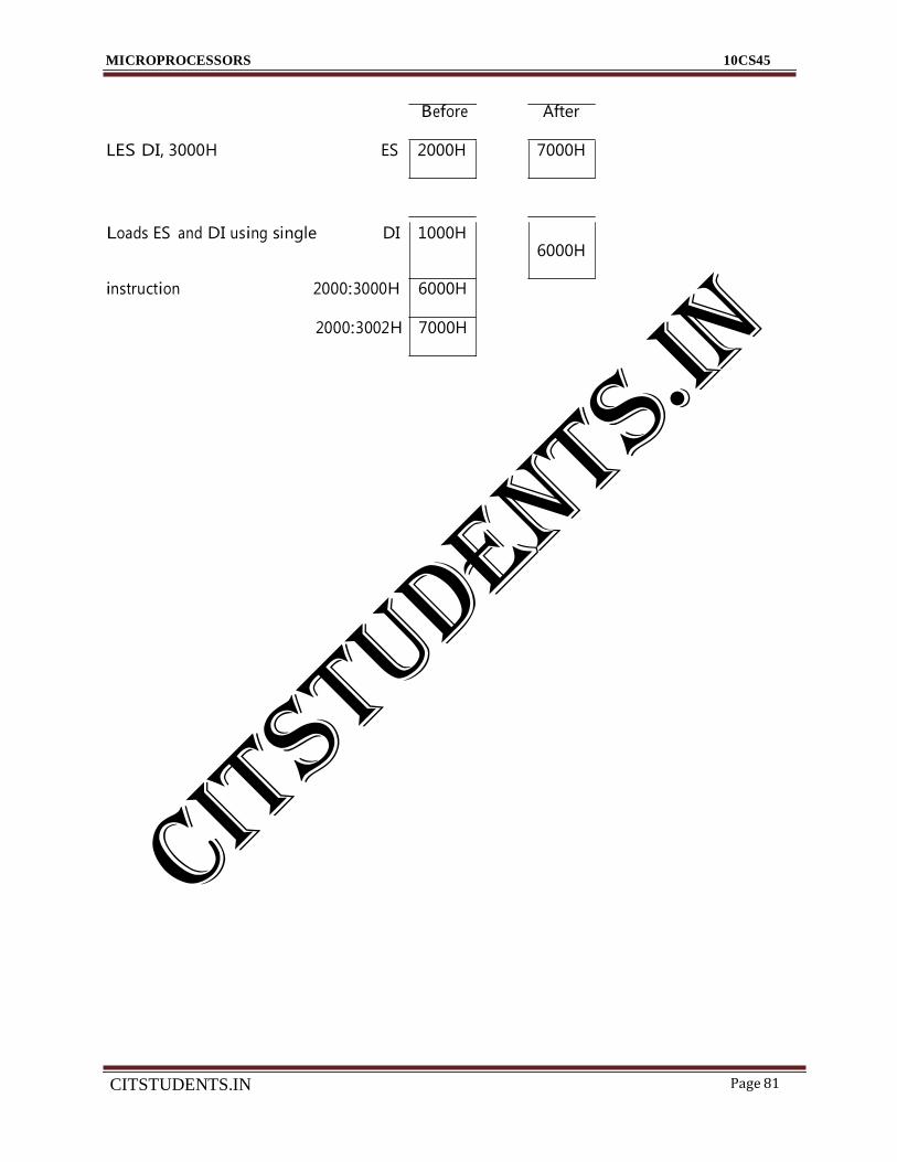
MICROPROCESSORS 10CS45
CITSTUDENTS.IN
Page 81
Before After
LES DI, 3000H ES 2000H 7000H
Loads ES and DI using single DI 1000H 6000H
instruction 2000:3000H 6000H
2000:3002H 7000H
CITSTUDENTS.IN

MICROPROCESSORS 10CS45
CITSTUDENTS.IN
Page 82
3.5 Operand instruction types
1 INC/ DEC/ NOT/NEG R/M
4 x (16+48) = 256 opcodes
2 PUSH/ POP R16/M16/SR/F
2 x (8+24+4+1) = 74 opcodes
3 MUL/ IMUL/ DIV/ DIV R/M
4 x (16+48) = 256 opcodes
Increment R16
INC BX 8 opcodes Before After
Ex. 1 BX 1234H 1235H
Ex. 2 BX FFFFH 0000H
Increment R8
INC DH 8 opcodes Before After
Ex. 1 DH 12H 13H
Ex. 2 DH FFH 00H
Increment M8
CITSTUDENTS.IN
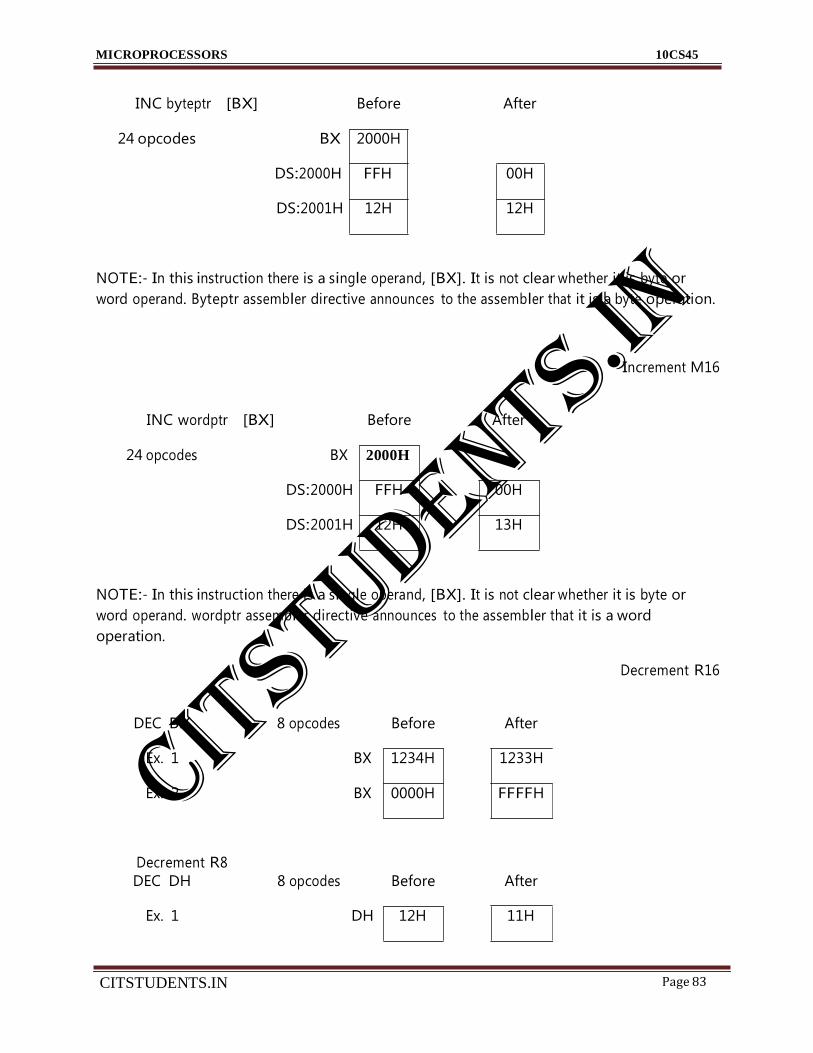
MICROPROCESSORS 10CS45
CITSTUDENTS.IN
Page 83
INC byteptr [BX] Before After
24 opcodes BX 2000H
DS:2000H FFH 00H
DS:2001H 12H 12H
NOTE:- In this instruction there is a single operand, [BX]. It is not clear whether it is byte or
word operand. Byteptr assembler directive announces to the assembler that it is a byte operation.
Increment M16
INC wordptr [BX] Before After
24 opcodes BX 2000H
DS:2000H FFH 00H
DS:2001H 12H 13H
NOTE:- In this instruction there is a single operand, [BX]. It is not clear whether it is byte or
word operand. wordptr assembler directive announces to the assembler that it is a word
operation.
Decrement R16
DEC BX 8 opcodes Before After
Ex. 1 BX 1234H 1233H
Ex. 2 BX 0000H FFFFH
Decrement R8
DEC DH
8 opcodes
Before
After
Ex. 1 DH 12H 11H
CITSTUDENTS.IN

MICROPROCESSORS 10CS45
CITSTUDENTS.IN
Page 84
Ex. 2 DH 00H FFH
Decrement M8
DEC byteptr [BX] Before After
24 opcodes BX 2000H
DS:2000H 00H FFH
DS:2001H 12H 12H
NOTE:-In this instruction there is a single operand, [BX]. It is not clear whether it is byte or word
operand. Byteptr assembler directive announces to the assembler that it is a byte operation. Decrement M16
DEC wordptr [BX] Before After
24 opcodes BX 2000H
DS:2000H 00H FFH
DS:2001H 12H 11H
NOTE:- In this instruction there is a single operand, [BX]. It is not clear whether it is byte or
word operand. wordptr assembler directive announces to the assembler that it is a word
operation.
Perform 1’s complement of R16
NOT BX 8 opcodes Before After
1234H BX
EDCBH CITSTUDENTS.IN

MICROPROCESSORS 10CS45
CITSTUDENTS.IN
Page 85
NOT operation performs 1’s complement.
Easy way: Subtract each hex digit from F
3.5.1 Perform 1’s complement of R8
NOT DH 8 opcodes Before After
DH 12H EDH
NOT byteptr
[BX]
Before
Perform 1’s complement of M8
After
24 opcodes BX 2000H
DS:2000H 23H DCH
DS:2001H 12H 12H
NOTE:- In this instruction there is a single operand, [BX]. It is not clear whether it is byte or
word operand. Byteptr assembler directive announces to the assembler that it is a byte operation.
Perform 1’s complement of M16
NOT wordptr [BX] Before After
24 opcodes BX 2000H
DS:2000H 34H CBH
DS:2001H 12H EDH
NOTE:- In this instruction there is a single operand, [BX]. It is not clear whether it is byte or
word operand. wordptr assembler directive announces to the assembler that it is a word
operation.
CITSTUDENTS.IN

MICROPROCESSORS 10CS45
CITSTUDENTS.IN
Page 86
Perform 2’s complement of R16
NEG BX 8 opcodes Before After
1234H BX
EDCCH
NEG operation performs 2’s complement.
Easy way: Subtract each hex digit from F and add 1
Perform 2’s complement of R8
NEG DH 8 opcodes Before After
DH 12H EEH
3.5.2 Perform 2’s complement of M8
NEG byteptr [BX] Before After
24 opcodes BX 2000H
DS:2000H 23H DDH
DS:2001H 12H 12H
NOTE:- In this instruction there is a single operand, [BX]. It is not clear whether it is byte or
word operand. Byteptr assembler directive announces to the assembler that it is a byte operation.
3.5.3 Perform 2’s complement of M16
NEG wordptr [BX] Before After
24 opcodes BX 2000H
CITSTUDENTS.IN

MICROPROCESSORS 10CS45
CITSTUDENTS.IN
Page 87
1122H Full 1234H
3344H 3344H
DS:2000H 34H CBH
DS:2001H 12H EDH
NOTE:- In this instruction there is a single operand, [BX]. It is not clear whether it is byte or
word operand. wordptr assembler directive announces to the assembler that it is a word
operation.
PUSH R16
Ex. PUSH CX Before After
CX 1234H
SP 5678H 5676H
Empty
Empty SS: 5676H
Full SS:5678H
Suppose SP content is 5678H. It means locations 5678, 567A, 567C … in stack segment are full.
Locations 5676, 5674, … are empty. Information pushed to location 5676 and SP value changes
to 5676H. Push operation is always on 16 bit data.
3.5.4 PUSH M16
Ex. PUSH [BX] Before After
BX 1234H
SP 3366H 3364H
DS:1234H 5678H
CITSTUDENTS.IN

MICROPROCESSORS 10CS45
CITSTUDENTS.IN
Page 88
Empty
Empty SP: 5676H 1122H Full 5678H
Full SP: 5678H 3344H 3344H
PUSH SR
Ex. PUSH CS Before After
CS 1234H
SP 5678H 5676H
Empty
Empty SS: 5676H 1122H Full 1234H
Full SS: 5678H 3344H 3344H
PUSH Flags
Ex. PUSHF Before After
Flags 1234H
SP 5678H 5676H
Empty
Empty SS: 5676H 1122H Full 1234H
Full SS: 5678H 3344H 3344H
POP R16
Ex. POP CX Before After
CITSTUDENTS.IN

MICROPROCESSORS 10CS45
CITSTUDENTS.IN
Page 89
CX 1234H 1122H
SP 5678H 567AH
Empty
Full SS: 5678H 1122H Empty 1122H
SS: 567AH 3344H Full 3344H
NOTE:- Suppose SP content is 5678H. It means locations 5678, 567A, 567C … in stack segment
are full. Locations 5676, 5674, … are empty. Information poped from location 5678 and SP
value changes to 567AH. Pop operation is always on 16 bit data.
POP M16
Ex. POP [BX] Before After
BX 1234H
SP 3366H 3368H
DS:1234H 5678H 1122H
Empty
Full SS: 3366H 1122H Empty 1122H
SS: 3368H 3344H Full 3344H
POP SR
Ex. POP CS Before After
CS 1234H 1122H
SP 5678H 567AH
Empty
CITSTUDENTS.IN

MICROPROCESSORS 10CS45
CITSTUDENTS.IN
Page 90
Full SS: 5678H 1122H Empty 1122H
SS: 567AH 3344H Full 3344H
POP Flags
Ex. POPF Before After
Flags 1234H 1122H
SP 5678H 567AH
Empty
Full SS: 5678H 1122H Empty 1122H
SS: 567AH 3344H Full 3344H
Unsigned Multiply R8 with AL and store product in AX
MUL CH Before After
CH FEH FEH
AL 02H FCH 01FCH = 508
AH 34H 01H
Unsigned Multiply R16 with AX and store product in DX AX
MUL CX Before After
CITSTUDENTS.IN

MICROPROCESSORS 10CS45
CITSTUDENTS.IN
Page 91
CX 00FEH 00FEH
AX 0002H 01FCH 01FCH = 508
DX 1234H 0000H
Signed Multiply R8 with AL and store product in AX
IMUL CH Before After
FEH = -02 CH FEH
AL 02H FCH FFFCH = -04
AH 34H FFH
NOTE:- IMUL CH instruction multiplies AL and CH treating them as signed numbers. The 16-
bit product is stored in AX.
Unsigned Division of AX by R8 and store quotient in AL and remainder in AH
DIV CH Before After
CH F0H
AL 25H 01H Quotient
AH 01H 35H Remainder
NOTE:- DIV CH instruction divides AX by CH treating them as unsigned numbers. The 8-bit
quotient is stored in AL and the 8-bit remainder stored in AH.
CITSTUDENTS.IN

MICROPROCESSORS 10CS45
CITSTUDENTS.IN
Page 92
Unsigned Division of DX AX by R16 and store quotient in AX and remainder in DX
DIV CX Before After
CX 00F0H
AX 0125H 0001H Quotient
DX 0000H 0035H Remainder
NOTE:- DIV CX instruction divides DX AX by CX treating them as unsigned numbers. The 16-
bit quotient is stored in AX and the 16-bit remainder stored in DX.
Signed Division of AX by R8 and store quotient in AL and remainder in AH
IDIV CH Before After
F0H = -10H CH F0H EE = -12H
AL 25H EEH Quotient
AH 01H 05H Remainder
NOTE:-IDIV CH instruction divides AX by CH treating them as signed numbers. The 8-bit
quotient is stored in AL and the 8-bit remainder stored in AH.
CITSTUDENTS.IN

MICROPROCESSORS 10CS45
CITSTUDENTS.IN
Page 93
3.5.5 8086 Instruction Template
Need for Instruction Template
8085 has 246 opcodes. The opcodes can be printed on an A4 size paper.
8086 has about 13000 opcodes. A book of about 60 pages is needed for printing the opcodes.
Concept of Template
In 8085, MOV r1, r2 (ex. MOV A, B) has the following template.
0 1 3-bit r1 code 3-bit r2 code
3-bit Register code Register
000 B
001 C
010 D
011 E
100 H
101 L
110 M
111 A
Ex. 1: Code for MOV A, B is
01 11 1 000 = 78H
7 8
Ex.2: Code for MOV M, D is
01 11 0 010 = 72H
CITSTUDENTS.IN

MICROPROCESSORS 10CS45
CITSTUDENTS.IN
Page 94
7 2
Using the template for MOV r1, r2 we can generate opcodes of 26 = 64 opcodes.
3.5.6 8086 Template for data transfer between REG and R/M
1 0 0 0 1 0 D W MOD REG R/M
2 bits 3 bits 3 bits
REG = A register of 8086 (8-bit or 16-bits) (except Segment registers, IP, and Flags registers)
Thus REG = AL/ BL/ CL/ DL/ AH/ BH/ CH/ DH/ AX/ BX/ CX/ DX/ SI/ DI/ BP/ SP
R/ M = Register (as defined above) or Memory contents (8-bits or 16-bits)
W = 1 means Word operation
W = 0 means Byte operation
D = 1 means REG is Destination register
D = 0 means REG is source register
MOD = 00 means R/M specifies Memory with no displacement
MOD = 01 means R/M specifies Memory with 8-bit displacement
MOD = 10 means R/M specifies Memory with 16-bit displacement
MOD = 11 means R/M specifies a Register
CITSTUDENTS.IN
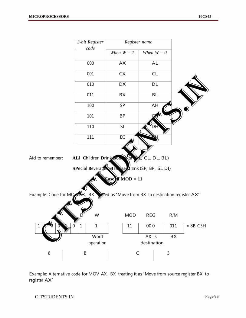
MICROPROCESSORS 10CS45
CITSTUDENTS.IN
Page 95
3-bit Register
code
Register name
When W = 1 When W = 0
000 AX AL
001 CX CL
010 DX DL
011 BX BL
100 SP AH
101 BP CH
110 SI DH
111 DI BH
Aid to remember: ALl Children Drink Bournvita (AL, CL, DL, BL)
SPecial Beverages SIamese DrInk (SP, BP, SI, DI)
Case of MOD = 11
Example: Code for MOV AX, BX treated as ‘Move from BX to destination register AX’
D W MOD REG R/M
1 0 0 0 1 0 1 1 11 00 0 011 = 8B C3H
Word
operation
AX is BX
destination
8 B C 3
Example: Alternative code for MOV AX, BX treating it as ‘Move from source register BX to
register AX’
CITSTUDENTS.IN

MICROPROCESSORS 10CS45
CITSTUDENTS.IN
Page 96
D W MOD REG R/M
1 0 0 0 1 0 0 1 11 01 1 000 = 89 D8H
Word
operation
BX is
source
AX
8 9 D 8
There are 2 possible opcodes for MOV AX, BX as we can choose either AX or BX as REG.
Example: Code for MOV AL, BH treated as ‘Move from BL to destination register AL’
D W MOD REG R/M
1 0 0 0 1 0 1 0 11 00 0 111 = 8A C7H
Byte
operation
AL is BH
destination
8 A C 7
Example: Alternative code for MOV AL, BH treating it as ‘Move from source register BH to
register AL’
D W MOD REG R/M
1 0 0 0 1 0 0 0 11 11 1 000 = 88 F8H
Byte
operation
BH is
source
AL
8 8 F 8
There are 2 possible opcodes for MOV AL, BH as we can choose either AL or BH as REG.
CITSTUDENTS.IN

MICROPROCESSORS 10CS45
CITSTUDENTS.IN
Page 97
Case of MOD = 00, 01 or 10
R/M MOD = 00
No
Displacement
MOD = 01
8-bit signed
displacement d8
MOD = 10
16-bit signed
displacement d16
000 [SI+BX] [SI+BX+d8] [SI+BX+d16]
001 [DI+BX] [DI+BX+d8] [DI+BX+d16]
010 [SI+BP] [SI+BP+d8] [SI+BP+d16]
011 [DI+BP] [DI+BP+d8] [DI+BP+d16]
100 [SI] [SI+d8] [SI+d16]
101 [DI] [DI+d8] [DI+d16]
110 [BP] Direct
Addressing
[BP+d8] [BP+d16]
111 [BX] [BX+d8] [BX+d16]
The table shows 24 memory addressing modes i.e. 24 different ways of accessing data stored in
memory.
Aid to remember:
SubInspector DIxit is a BoXer ( [SI+BX] and [DI]+[BX] )
SubInspector DIxit knows to control BP ( [SI+BP] and [DI]+[BP] )
He says’ SImple DIet DIRECTs a BoXer' ( [SI], [DI], Direct addressing, [BX] ) CITSTUDENTS.IN

MICROPROCESSORS 10CS45
CITSTUDENTS.IN
Page 98
Ex: Code for MOV CL, [SI]
D W MOD REG R/M
1 0 0 0 1 0 1 0 00 00 1 100 = 8A 0CH
Byte No CL is [SI]
operation Disp. destination
8 A 0 C
Note that there is a unique opcode for MOV CL, [SI] as CL only can be REG.
Ex: Code for MOV 46H[BP], DX
D W MOD REG R/M d8
1 0 0 0 1 0 0 1 01 01 0 110 46H = 89 56 46H
Word 8-bit DX is [BP+d8]
operation Disp. source
8 9 5 6
Note that there is a unique opcode for MOV 46H[BP], DX as DX only can be REG.
Ex: Code for MOV 0F246H[BP], DX
CITSTUDENTS.IN

MICROPROCESSORS 10CS45
CITSTUDENTS.IN
Page 99
D W MOD REG R/M d16
1 0 0 0 1 0 0 1 10 01 0 110 F2 46H = 89 96 F2 46H
Word 16-bit DX is [BP+d16] Stored as 89 96
operation Disp. source 46 F2H
8 9 9 6 in Little Endian
Note that there is a unique opcode for MOV 0F246H[BP], DX as DX only can be REG.
Ex: Code for MOV [BP], DX
D W MOD REG R/M d8
1 0 0 0 1 0 0 1 01 01 0 110 00H = 89 56 00H
Word 8-bit DX is [BP+d8]
operation Disp. source
8 9 5 6
Note that MOV [BP], DX is treated as MOV 00H[BP], DX before coding.
Ex: Code for MOV BX, DS:1234H
D W MOD REG R/M Direct
addr
1 0 0 0 1 0 1 1 00 01 1 110 12
34H
= 8B 1E 12 34H
Word No BX is Direct Stored as 8B 1E
operation Disp. Dest. addr. 34 12H
8 B 1 E In Little Endian
Note that when MOD = 00 and R/M = 110, it represents Direct Addressing.
CITSTUDENTS.IN

MICROPROCESSORS 10CS45
CITSTUDENTS.IN
Page 100
4.1 Branch group of instructions
Unit 4
Branch instructions provide lot of convenience to the programmer to perform operations selectively,
repetitively etc.
Branch group of instructions
Conditional
jumps
Uncondi-tional
jump
Iteration
instructions
CALL instructions Return
instructions
Conditional Jump instructions
Conditional Jump instructions in 8086 are just 2 bytes long. 1-byte opcode followed by 1-byte signed
displacement (range of –128 to +127).
Conditional Jump Instructions
Jumps based on a single flag Jumps based on more than one flag
Jumps Based on a single flag
JZ r8
JNZ r8
JS r8
JNS r8
JC r8
JNC r8
;Jump if zero flag set (if result is 0). JE also means same.
;Jump if Not Zero. JNE also means same.
;Jump if Sign flag set to 1 (if result is negative)
;Jump if Not Sign (if result is positive)
;Jump if Carry flag set to 1. JB and JNAE also mean same.
;Jump if No Carry. JAE and JNB also mean same.
JP r8 ;Jump if Parity flag set to 1. JPE (Jump if Parity Even) also means same.
CITSTUDENTS.IN

MICROPROCESSORS 10CS45
CITSTUDENTS.IN
Page 101
CMP SI, DI
JE SAME
ADD CX, DX
:
:
SUB BX, AX
Exa
mpl
es
for
JE
or
JNP r8
JO r8
JNO r8
;Jump if No Parity. JPO (Jump if Parity Odd) also means same.
;Jump if Overflow flag set to 1 (if result is wrong)
;Jump if No Overflow (if result is correct)
JZ
inst
ruc
tion
JE is abbreviation for Jump if Equal. JB is abbreviation for Jump if Below.
JNE is abbreviation for Jump if Not Equal. JNAE is for Jump if Not Above or Equal.
JZ, JNZ, JC and JNC used after arithmetic operation
Ex.
for
JE, JNE, JB, JNAE, JAE and JNB are used after a compare operation.
forward jump
Only examples using JE instruction given for forward and backward jumps.
;Executed if Z = 0
Should be<=127 bytes (if SI not equal to DI)
SAME: ;Executed if Z = 1
(if SI = DI)
CITSTUDENTS.IN

MICROPROCESSORS 10CS45
CITSTUDENTS.IN
Page 102
SUB BX,AX
:
:
CMP SI, DI
JE BACK
ADD CX,DX
Ex. for backward jump
BACK: ;Executed if Z = 1 (if SI=DI)
Should be <=127
bytes
;Executed if Z = 0 (if SI <> DI)
Jumping beyond -128 to +127?
Requirement Then do this!
CMP SI, DI CMP SI, DI
JE SAME JNE NEXT
What if ADD CX, DX JMP SAME
>127 bytes : NEXT: ADD CX, DX
: :
SAME: SUB BX, AX :
SAME: SUB BX, AX
15
Range for JMP (unconditional jump) can be +2 = + 32K. JMP instruction discussed in detail later
CITSTUDENTS.IN

MICROPROCESSORS 10CS45
CITSTUDENTS.IN
Page 103
4.2 Terms used in comparison
Above and Below used for comparing Unsigned numbers. Greater than and less than used when
comparing signed numbers. All Intel microprocessors use this convention.
Accordingly, all the following statements are true.
95H is above 65H
95H is less than 65H
65H is below 95H
65H is greater than 95H
Unsigned comparison - True
Signed comparison – True (as 95H is negative, 65H is positive)
Unsigned comparison - True
Signed comparison - True
4.2.1 Jump based on multiple flags
Conditional Jumps based on multiple flags are used after a CMP (compare) instruction.
JBE / JNA instruction
‘Jump if Below or Equal’ or ‘Jump if Not Above’
Jump if No Jump if Ex.
Cy = 1 OR Z= 1 Cy = 0 AND Z = 0 CMP BX, CX
Below OR Equal Surely Above JBE BX_BE
CITSTUDENTS.IN

MICROPROCESSORS 10CS45
CITSTUDENTS.IN
Page 104
4.2.2 BX_BE (BX is Below or Equal) is a symbolic location
4.2.3 JNBE / JA instruction
‘Jump if Not (Below or Equal)’ or ‘Jump if Above’
Jump if No Jump if Ex.
Cy = 0 AND Z= 0 Cy = 1 OR Z = 1 CMP BX, CX
Surely Above Below OR Equal JBE BX_BE
4.2.4 JLE / JNG instruction
‘Jump if Less than OR Equal’ or ‘Jump if Not Greater than’
Jump if No Jump if
[(S=1 AND V=0) OR (S=0 AND V=0)] OR
Z=1
[(S=0 AND V=0) OR (S=1 AND V=1)] AND
Z=0
[(surely negative) or (wrong answer positive!)] [(surely positive) or (wrong answer negative!)]
or Equal and not equal
i.e. [S XOR V=1] OR Z=1 i.e.[S XOR V=0] AND Z=0
CITSTUDENTS.IN

MICROPROCESSORS 10CS45
CITSTUDENTS.IN
Page 105
JNLE / JG instruction
‘Jump if Not (Less than OR Equal)’ or ‘Jump if Greater than’
Jump if No Jump if
[(S=0 AND V=0) OR (S=1 AND V=1)] AND
Z=0
[(S=1 AND V=0) OR (S=0 AND V=1)] OR
Z=1
[(surely positive) or (wrong answer negative!)]
and not equal
[(surely negative) or (wrong answer positive!)]
or equal
i.e. S XOR V=0 AND Z=0 i.e.S XOR V=1 OR Z=1
4.2.4 JL / JNGE instruction
‘Jump if Less than’ or ‘Jump if NOT (Greater than or Equal)’
Jump if No Jump if
[S=1 AND V=0] OR [S=0 AND V=1] [S=0 AND V=0] OR [S=1 AND V=1]
(surely negative)or (wrong answer
positive!)
(surely positive) or (wrong answer
negative!)
i.e. S XOR V=1 i.e.S XOR V=0
Note: When S=1, result cannot be 0 CITSTUDENTS.IN

MICROPROCESSORS 10CS45
CITSTUDENTS.IN
Page 106
4.2.5 JNL / JGE instruction
‘Jump if Not Less than’ or ‘Jump if Greater than OR Equal’
Jump if No Jump if
[S=0 AND V=0] OR (S=1 AND V=1) [S=1 AND V=0] OR (S=1 AND V=1)
(surely positive) or (wrong answer negative!) (surely negative) or (wrong answer positive!)
i.e. S XOR V=0 i.e.S XOR V=1
Note: When S=0, result can be >= 0
Unconditional Jump instruction
Unconditional Jump Instruction
Near Jump or Intra segment Jump Far Jump or Inter segment Jump
(Jump within the segment) (Jump to a different segment)
Near Unconditional Jump instruction
Near Jump
Direct Jump (common) Indirect Jump (uncommon)
2-bytes Short Jump (EB r8) 3-bytes Long Jump (E9 r16) 2 or more bytes
CITSTUDENTS.IN

MICROPROCESSORS 10CS45
CITSTUDENTS.IN
Page 107
7 15
Range: + 2 Range: +2 Starting with FFH
Range: complete segment
Three Near Jump and two Far Jump instructions have the same mnemonic JMP, but they have
different opcodes
4.2.5 Short Jump Instruction
2 byte (EB r8) instruction with Range: -128 to +127 bytes
For Backward jump: Assembler knows the quantum of jump. Generates Short Jump code if
<=128 bytes is the required jump. Generates code for Long Jump if >128 bytes is the required
jump.
For Forward jump: Assembler doesn’t know jump quantum in pass 1. Assembler reserves 3
bytes for the forward jump instruction. If jump distance turns out to be >128 bytes, the instruction
is coded as E9 r16 (E9H = Long jump code). If jump distance becomes <=128 bytes, the
instruction is coded as EB r8 followed by code for NOP (E8H = Short jump code).
CITSTUDENTS.IN

MICROPROCESSORS 10CS45
CITSTUDENTS.IN
Page 108
:
:
JMP FRWD
:
:
:
4.2.5 SHORT Assembler Directive
Assembler generates only 2 byte Short Jump code for forward jump, if the SHORT assembler
directive is used.
JMP SHORT SAME
:
Programmer should ensure that
the Jump distance is <=127 bytes
SAME:
:
MOV CX, DX
Long Jump instruction
3-byte (E9 r16) instruction with Range: -32768 to +32767 bytes
Long Jump can cover entire 64K bytes of Code segment
CS:0000H
CS:8000H
Long Jump can handle it as jump
quantum is <=32767
FRWD = CS:FFFFH CITSTUDENTS.IN

MICROPROCESSORS 10CS45
CITSTUDENTS.IN
Page 109
:
:
JMP BKWD
:
:
:
:
JMP FRWD
:
:
:
:
:
:
:
:
JMP BKWD
:
:
Long Jump can handle it as jump
quantum is <=32767
BKWD= CS:0000H
CS:8000H
FRWD = CS:FFFFH
4.2.6 Long Jump or Short Jump?
Can be treated as a
small (20H) Backward
Branch!
CS:0000H
CS:0010H
Jump distance =FFE0H.
Too very long forward
jump.
FRWD = CS:FFF0H
CS:FFFFH
Can be treated as a small
(20H)
Forward Branch!
CS:0000H
BKWD = CS:0010H
Jump distance =FFE0H.
Too very long
backward jump
CS:FFF0H
CS:FFFFH
CITSTUDENTS.IN

MICROPROCESSORS 10CS45
CITSTUDENTS.IN
Page 110
4.2.7 Intra segment indirect Jump
It is also called Near Indirect Jump. It is not commonly used.
Instruction length: 2 or more bytes Range: complete segment
Ex.1: JMP DX
If DX = 1234H, branches to CS:1234H. 1234H is not signed relative displacement.
Ex. 2: JMP wordptr 2000H[BX]
If BX contents is 1234H DS:3234H 5678H
Branches to CS:5678H DS:3236H AB22H
Far Jump instruction
4.2.8 Far Jump
Direct Jump (common) Indirect Jump (uncommon)
5 bytes, opcode EA, 2 byte offset, 2 or more bytes,
2 byte segment value starting with opcode FFH
Range: anywhere in memory Range: anywhere in memory
As stated earlier, three Near Jump and two Far Jump instructions have the same mnemonic
JMP but different opcodes.
CITSTUDENTS.IN

MICROPROCESSORS 10CS45
CITSTUDENTS.IN
Page 111
4.2.9 Inter segment Direct Jump instruction
Also called Far Direct Jump. It is the common inter segment jump scheme
It is a 5 byte instruction. 1 byte opcode (EAH), 2 byte offset value, 2 byte segment value
Ex. JMP Far ptr LOC
4.2.10 Inter segment Indirect Jump instruction
Also called Far Indirect Jump. It is not commonly used. Instruction length depends on the way
jump location is specified. It can be a minimum of 2 bytes.
Ex. JMP DWORD PTR 2000H[BX]
If BX contents is 1234H branch takes place to location ABCDH:5678H. It is a 4-byte instruction.
DS:3234H 5678H
DS:3236H ABCDH
Iteration Instructions
Iteration instructions provide a convenient way to implement loops in a program
Iteration instructions
LOOP LOOPZ or LOOPE LOOPNZ or LOOPNE JCXZ
CITSTUDENTS.IN
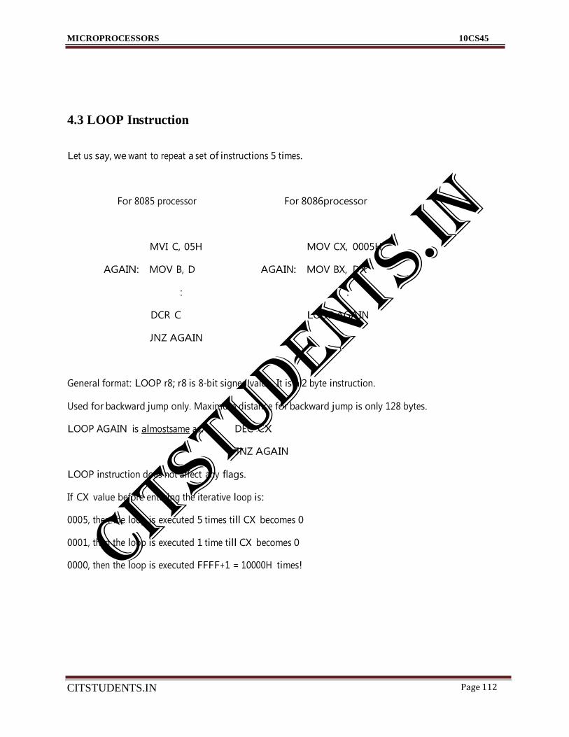
MICROPROCESSORS 10CS45
CITSTUDENTS.IN
Page 112
4.3 LOOP Instruction
Let us say, we want to repeat a set of instructions 5 times.
For 8085 processor For 8086processor
MVI C, 05H MOV CX, 0005H
AGAIN: MOV B, D AGAIN: MOV BX, DX
: :
DCR C LOOP AGAIN
JNZ AGAIN
General format: LOOP r8; r8 is 8-bit signed value. It is a 2 byte instruction.
Used for backward jump only. Maximum distance for backward jump is only 128 bytes.
LOOP AGAIN is almost same as: DEC CX
JNZ AGAIN
LOOP instruction does not affect any flags.
If CX value before entering the iterative loop is:
0005, then the loop is executed 5 times till CX becomes 0
0001, then the loop is executed 1 time till CX becomes 0
0000, then the loop is executed FFFF+1 = 10000H times! CITSTUDENTS.IN

MICROPROCESSORS 10CS45
CITSTUDENTS.IN
Page 113
MOV CX, SI
JCXZ SKIP
MOV BX, DX
:
:
LOOP AGAIN
ADD SI, DI
4.3.1 JCXZ Instruction
Jump if CX is Zero is useful for terminating the loop immediately if CX value is 0000H It is a 2
byte instruction. It is used for forward jump only. Maximum distance for forward jump is only
127 bytes.
Ex.
AGAIN:
SKIP: ; Executed after JCXZ if CX = 0
CITSTUDENTS.IN

MICROPROCESSORS 10CS45
CITSTUDENTS.IN
Page 114
4.3.2 LOOPZ instruction
LOOP while Zero is a 2-byte instruction. It is used for backward jump only. Backward jump
takes place if after decrement of CX it is still not zero AND Z flag = 1. LOOPE is same as
LOOPZ. LOOPE is abbreviation for LOOP while Equal. LOOPE is normally used after a
compare instruction.
Ex. MOV CX, 04H
BACK: SUB BX, AX
MOV BX, DX
:
:
ADD SI, DI
LOOPZ BACK ; if SI+DI = 0 and CX not equal to 0, branch to BACK
4.3.3 CALL Instructions
CALL instruction is used to branch to a subroutine. There are no conditional Call instructions in
8086.
CALL instructions
Near CALL or Intra segment CALL Far CALL or Inter segment CALL
Near Direct CALL Near Indirect CALL Far Direct CALL Far Indirect CALL
CITSTUDENTS.IN

MICROPROCESSORS 10CS45
CITSTUDENTS.IN
Page 115
4.3.4 Near Direct CALL instruction
It is a 3-byte instruction. It has the format CALL r16 and has the range + 32K bytes.
Covers the entire Code segment. It is the most common CALL instruction.
It is functionally same as the combination of the instructions PUSH IP and ADD IP, r16.
Ex. CALL Compute
4.3.5 Near Indirect CALL instruction
Not commonly used. Instruction length depends on the way the called location is specified.
Ex.1: CALL AX ; If (AX) = 1234H, branches to procedure at CS: 1234H.
1234H is not relative displacement.
Ex. 2: CALL word ptr 2000H[BX]
If BX contents is1234H Branches to subroutine at CS:5678H
DS:3234H 5678H
DS:3236H ABCDH
Far Direct CALL instruction
It is a 5-byte instruction. 1-byte opcode, 2-byte offset, 2-byte segment value.
Far direct CALL is functionally same as:
PUSH CS
CITSTUDENTS.IN

MICROPROCESSORS 10CS45
CITSTUDENTS.IN
Page 116
PUSH IP
IP = 2-byte offset value provided in CALL
CS = 2-byte segment value provided in CALL
Ex. CALL far ptr Compute
4.3.6 Far Indirect CALL instruction
Not commonly used. Instruction length depends on the way the called location is specified.
Ex. CALL dword ptr 2000H[BX]
If BX contents is1234H bBranches to subroutine at ABCDH:5678H
DS:3234H 5678H
DS:3236H ABCDH
4.3.7 Conditional CALL?
What if we want to branch to subroutine COMPUTE only if Cy flag = 0?
Solution:
JC NEXT
CALL COMPUTE ; execute only if Cy = 0
NEXT: CITSTUDENTS.IN
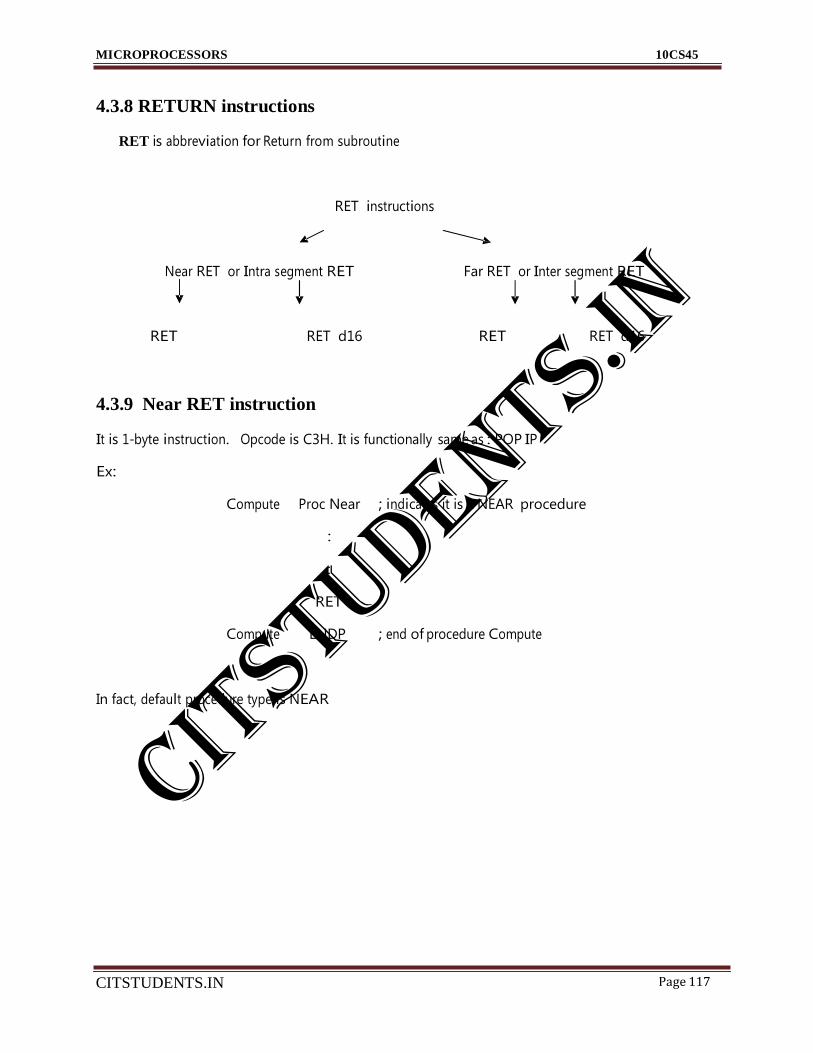
MICROPROCESSORS 10CS45
CITSTUDENTS.IN
Page 117
4.3.8 RETURN instructions
RET is abbreviation for Return from subroutine
RET instructions
Near RET or Intra segment RET Far RET or Inter segment RET
RET RET d16 RET RET d16
4.3.9 Near RET instruction
It is 1-byte instruction. Opcode is C3H. It is functionally same as : POP IP
Ex:
Compute Proc Near ; indicates it is a NEAR procedure
:
:
RET
Compute ENDP ; end of procedure Compute
In fact, default procedure type is NEAR
CITSTUDENTS.IN
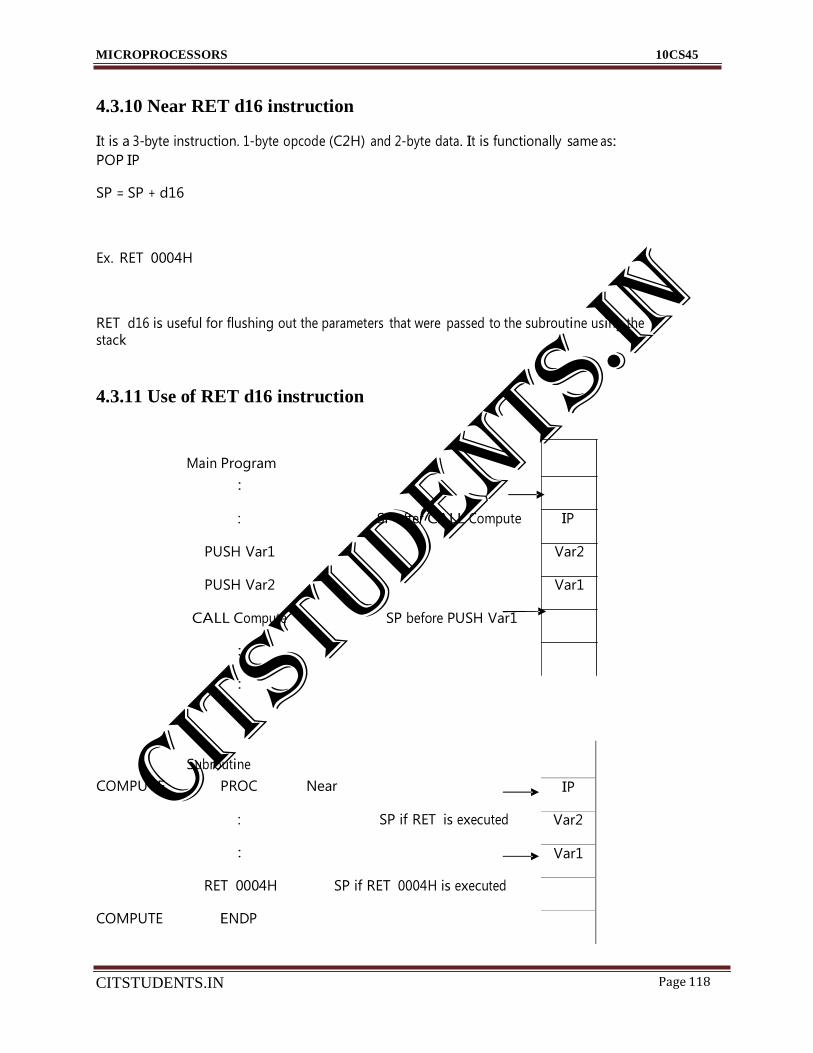
MICROPROCESSORS 10CS45
CITSTUDENTS.IN
Page 118
IP
Var2
Var1
4.3.10 Near RET d16 instruction
It is a 3-byte instruction. 1-byte opcode (C2H) and 2-byte data. It is functionally same as:
POP IP
SP = SP + d16
Ex. RET 0004H
RET d16 is useful for flushing out the parameters that were passed to the subroutine using the stack
4.3.11 Use of RET d16 instruction
Main Program
:
: SP after CALL Compute IP
PUSH Var1 Var2
PUSH Var2 Var1
CALL Compute SP before PUSH Var1
:
:
COMPUTE
Subroutine
PROC Near
: SP if RET is executed
:
RET 0004H SP if RET 0004H is executed
COMPUTE ENDP
CITSTUDENTS.IN

MICROPROCESSORS 10CS45
CITSTUDENTS.IN
Page 119
Far RET instruction
It is 1-byte instruction. Opcode is CBH. It is functionally same as: POP IP + POP CS
Ex. SINX Proc Far ; indicates it is a FAR procedure
:
:
RET
SINX ENDP ; end of procedure SINX
Default procedure type is NEAR
4.3.12 Far RET d16 instruction
It is a 3-byte instruction. 1-byte opcode (CAH) and 2-byte data.
It is functionally same as: POP IP + POP CS + ADD SP, d16
Ex. RET 0006H
RET d16 is useful for flushing out the parameters that were passed to the subroutine using the
stack.
CITSTUDENTS.IN

MICROPROCESSORS 10CS45
CITSTUDENTS.IN
Page 120
Unit -5
5.1 Mixing Assembly and C
Often it is a good idea to link assembly language programs or routines with high-level programs
which may contain resources unavailable to you through direct assembly programming--such as
using C's built in graphics library functions or string-processing functions. Conversely, it is often
necessary to include short assembly routines in a compiled high-level program to take advantage
of the speed of machine language.
All high-level languages have specific calling conventions which allow one language to
communicate
to the
other;
i.e.,
to send
variables,
values,
etc. The assembly-language program
that is written in conjunction with the high-level language must also reflect these conventions if
the
two
are
to be
successfully
integrated.
Usually high-level
languages
pass
parameters to
subroutines by utilizing the stack. This is also the case for C.
5.2 Using Assembly Procedures in C Functions
5.2 .1 Procedure Setup
In order to ensure that the assembly language procedure and the C program will combine and be
compatible, the following steps should be followed:
• Declare the procedure label global by using the GLOBAL directive. In addition, also
declare global any data that will be used.
• Use the EXTERN directive to declare global data and procedures as external. It is best to
place the EXTERN statement outside the segment definitions and to place near data inside
the data segment.
• Follow
the C
naming
conventions--i.e.,
precede
all
names
(both
procedures
and
data)
with underscores.
CITSTUDENTS.IN

MICROPROCESSORS 10CS45
CITSTUDENTS.IN
Page 121
5.2 .2 Stack Setup
Whenever entering a procedure, it is necessary to set up a stack frame on which to pass
parameters. Of
course,
if the
procedure
doesn't
use
the
stack,
then it
is not
necessary. To
accomplish the stack setup, include the following code in the procedure:
push
mov
ebp
ebp,
esp
EBP allows us to use this pointer as an index into the stack, and should not be altered throughout
the
procedure
unless
caution is
taken.
Each
parameter
passed
to the
procedure
can
now be
accessed as an offset from EBP. This is commonly known as a "standard stack frame."
5.2 .3 Preserving Registers
It is necessary that the procedure preserve the contents of the registers ESI, EDI, EBP, and all
segment registers. If these registers are corrupted, it is possible that the computer will produce
errors when returning to the calling C program.
5.2 .4 Passing Parameters in C to the Procedure
C passes arguments to procedures on the stack. For example, consider the following statements
from a C main program:
extern
int
|
Sum();
|
int
a1,
a2, x;
|
x = Sum(a1,
a2);
When C executes the function call to Sum, it pushes the input arguments onto the stack in
reverse order, then executes a call to Sum. Upon entering Sum, the stack would contain the
following:
CITSTUDENTS.IN

MICROPROCESSORS 10CS45
CITSTUDENTS.IN
Page 122
Since a1 and a2 are declared as int variables, each takes up one word on the stack. The above
method of passing input arguments is called passing by value. The code for Sum, which outputs
the sum of the input arguments via register EAX, might look like the following:
_Sum
push
mov
ebp
ebp,
esp
; create stack frame
mov eax, [ebp+8] ; grab the first argument
mov
add
pop
ecx,
eax,
ebp
[ebp+12]
ecx
;
;
;
grab the second argument
sum the arguments
restore the base pointer
ret
It is interesting to note several things. First, the assembly code returns the value of the result to
the C program through
EAX implicitly. Second, a simple RET statement is all that is necessary
when
returning
from
the
procedure. This
is due to
the
fact
that
C takes
care
of removing the
passed parameters from the stack.
Unfortunately, passing by value has the drawback that we can only return one output value.
What if Sum must output several values, or if Sum must modify one of the input variables? To
accomplish this, we must pass arguments by reference. In this method of argument transmission,
the addresses of the arguments are passed, not their values. The address may be just an offset, or
both an offset and a segment. For example, suppose Sum wishes to modify a2 directly--perhaps
storing the result in a2 such that a2 = a1 + a2. The following function call from C could be used:
Sum(a1, &a2);
The first argument is still passed by value (i.e., only its value is placed on the stack), but the
second
argument is
passed
by reference (its
address
is placed
on the
stack).
The
"&"
prefix
CITSTUDENTS.IN

MICROPROCESSORS 10CS45
CITSTUDENTS.IN
Page 123
means "address of." We say that &a2 is a "pointer" to the variable a2. Using the above statement,
the stack would contain the following upon entering Sum:
Note that the address of a2 is pushed on the stack, not its value. With this information, Sum can
access the variable a2 directly. (Hint: use an index register to hold the offset, then use a memory
access to access the variable).
5.2 .5 Returning a Value from the Procedure
Assembly can return values to the C calling program using only the EAX register. If the returned
value is only four bytes or less, the result is returned in register EAX. If the item is larger than
four bytes, a pointer is returned in EAX which points to the item. Here is a short table of the C
variable types and how they are returned by the assembly code:
Data Type
char
short
Register
AL
AX
int, long, pointer
(*)
EAX
5.2 .6 Allocating Local Data Space on the Stack
Temporary storage space for local variables or data can be created by decreasing the contents of
ESP just after setting up a stack frame at the beginning of the procedure. It is important to restore
the stack space at the end of the procedure. The following code fragment illustrates the basic
idea:
push ebp ; Save caller's stack frame
CITSTUDENTS.IN

MICROPROCESSORS 10CS45
CITSTUDENTS.IN
Page 124
mov ebp, esp ; Establish new stack frame
sub
esp, 4 ;
Allocate
local
data
space of
; 4 bytes
push
push
...
esi ;
edi
Save
critical
registers
pop
pop
edi ;
esi
Restore
critical
registers
mov
esp,
ebp
; Restore
the
stack
pop
ebp ;
Restore
the
frame
ret ;
Return
to caller
5.2 .7 Using C Functions in Assembly Procedures
In most cases, calling C library routines or functions from an assembly program is more complex
than calling assembly programs from C. An example of how to call the printf library function
from within an assembly program is shown next, followed by comments on how it actually
works.
global _main
extern _printf
section .data
text db "291 is the best!", 10, 0
strformat db
"%s", 0
section .code
_main push
dword
text
CITSTUDENTS.IN

MICROPROCESSORS 10CS45
CITSTUDENTS.IN
Page 125
push dword strformat
call
_printf
add
ret
esp, 8
Notice that the procedure is declared global, and its name must be _main, which is the starting
point of all C code.
Since C pushes its arguments onto the stack in reverse order, the offset of the string is pushed
first, followed by the offset of the format string. The C function can then be called, but care must
be taken to restore the stack once it has completed.
When linking the assembly code, include the standard C library (or the library containing the
functions you use) in the link. For a more detailed (and perhaps more accurate) description of the
procedures involved in calling C functions, refer to another text on the subject.
CITSTUDENTS.IN

MICROPROCESSORS 10CS45
CITSTUDENTS.IN
Page 126
GND
1
AD14 2
AD13 3
AD12 4
AD11 5
AD10 6
AD9 7
AD8 8
AD7 9
AD6 10
AD5 11
AD4 12
AD3 13
AD2 14
AD1 15
AD0 16
NMI 17
INTR 18
CLK 19
GND 20
30
Unit-6
6.1 Pin Configuration
40
39
38
37
36
35
34
33
32
8086 31
29
28
27
26
25
24
23
22
21
Vcc AD15
A16/S3
A17/S4
A18/S5
A19/S6
BHE/S7
MN/MX
RD
RG/GT0 (HOLD)
RQ/GT1 (HLDA)
LOCK (WR)
S2 (M/I0)
S1 (DT/R)
S0 (DEN)
QS0 (ALE)
QS1 (INTA)
TEST
READY
RESET
Fig. .1 Pin Configuration
The following pin function descriptions are for the microprocessor 8086 in either minimum or
maximum mode. The 8086 pins signals are TTL compatible.
6.1 AD0 - AD15 (I/O): Address Data Bus
These lines constitute the time multiplexed memory/IO address during the first clock cycle
(T1) and data during T2, T3 and T4 clock cycles. A0 is analogous to BHE for the lower byte of
the data bus, pins D0-D7.
A0 bit is Low during T1 state when a byte is to be transferred on the
lower
portion of
the
bus
in memory or
I/O
operations. 8-bit
oriented
devices
tied to
the
lower
half
would
normally
use
A0 to
condition
chip select
functions. These lines
are
active
high
and
float to tri-state during interrupt acknowledge and local bus "Hold acknowledge".
the timing of AD0 – AD15 lines to access data and address.
Fig. 2 shows
CITSTUDENTS.IN

MICROPROCESSORS 10CS45
CITSTUDENTS.IN
Page 127
T4 T1 T2 T3 T4
AD0 - AD15 Address Data
Fig. .2
6.1.1 A19/S6, A18/S5, A17/S4, A16/S3 (0): Address/Status
During T1 state these lines are the four most significant address lines for memory
operations. During I/O operations these lines are low. During memory and I/O operations, status
information is available on these lines during
T2, T3, and T4 states.
S5: The status of the interrupt enable flag bit is updated at the beginning of each cycle.
The status of the flag is indicated through this bus.
S6: When Low, it indicates that 8086 is in control of the bus. During a "Hold
acknowledge" clock period, the 8086 tri-states the S6 pin and thus allows another bus master to
take control of the status bus.
S3 & S4: Lines are decoded as follows:
A17/S4 A16/S3 Function
0 0 Extra segment access
0 1 Stack segment access
1 0 Code segment access
1 1 Data segment access
Table 1
After the first clock cycle of an instruction execution, the A17/S4 and A16/S3 pins specify which
segment register generates the segment portion of the 8086 address. Thus by decoding these lines and
using the decoder outputs as chip selects for memory chips, up to 4 Megabytes (one Mega per segment)
of memory can be accesses. This feature also provides a degree of protection by preventing write
CITSTUDENTS.IN

MICROPROCESSORS 10CS45
CITSTUDENTS.IN
Page 128
operations to one segment from erroneously overlapping into another segment and destroying information
in that segment.
6.1.2 BHE /S7 (O): Bus High Enable/Status
During T1 state the BHE should be used to enable data onto the most significant half of the data
bus, pins D15 - D8. Eight-bit oriented devices tied to the upper half of the bus would normally use BHE
to control chip select functions. BHE is Low during T1 state of read, write and interrupt acknowledge
cycles when a byte is to be transferred on the high portion of the bus.
The S7 status information is available during T2, T3 and T4 states. The signal is active Low and
floats to 3-state during "hold" state. This pin is Low during T1 state for the first interrupt acknowledge
cycle.
6.1.3 RD (O): READ
The Read strobe indicates that the processor is performing a memory or I/O read cycle. This signal is
active low during T2 and T3 states and the Tw states of any read cycle.
This signal floats to tri-state in "hold acknowledge cycle".
TEST (I)
TEST pin is examined by the "WAIT" instruction. If the TEST pin is Low, execution
continues.
Otherwise
the
processor
waits in an
"idle" state.
This
input is
synchronized internally during each clock cycle on the leading edge of CLK.
6.1 .4 INTR (I):
Interrupt Request
It is a level triggered input which is sampled during the last clock cycle of each instruction to
determine if the processor should enter into an interrupt acknowledge operation. A subroutine is vectored
to via an interrupt vector look up table located in system memory. It can be internally masked by software
resetting the interrupt enable bit
INTR is internally synchronized. This signal is active HIGH.
CITSTUDENTS.IN

MICROPROCESSORS 10CS45
CITSTUDENTS.IN
Page 129
6.1 .5 NMI (I): Non-Muskable Interrupt
An edge triggered input, causes a type-2 interrupt. A subroutine is vectored to via the interrupt
vector look up table located in system memory.
NMI is not maskable
internally by
software. A
transition from a LOW to HIGH on this pin initiates the
interrupt at the end of the current instruction. This input is internally synchronized.
6.1 .6 Reset (I)
Reset causes the processor to immediately terminate its present activity. To be recognised, the
signal must be active high for at least four clock cycles, except after power-on which requires a 50 Micro
Sec. pulse. It causes the 8086 to initialize registers DS, SS, ES, IP and flags to all zeros. It also initializes
CS to FFFF H. Upon removal of the RESET signal from the RESET pin, the 8086 will fetch its next
instruction from the 20 bit physical address FFFF0H. The reset signal to 8086 can be generated by the
8284. (Clock generation chip). To guarantee reset from power-up, the reset input must remain below 1.5
volts for 50 Micro sec. after Vcc has reached the minimum supply voltage of 4.5V. The RES input of the
8284 can be driven by a simple RC circuit as shown in fig.3.
X1
X2
F/C
R
8284
CLK
CLK
8086 µp
+5V Normal Reset Key
RES
C
RESET RESET
SYSTEM RESET
Fig. .3
The value of R and C can be selected as follows:
Vc (t) = V (1 - e -t /RC)
t = 50 Micro sec.
V = 4.5 volts, Vc = 1.05V and RC = 188 Micro sec.
C = 0.1 Micro F; R = 1.88 K ohms.
CPU component Contents
Flags Cleared
CITSTUDENTS.IN

MICROPROCESSORS 10CS45
CITSTUDENTS.IN
Page 130
Instruction Pointer 0000H
CS register FFFFH
DS register 0000H
SS register 0000H
ES register 0000H
Queue Empty
Table – .2 System Registers after Reset
8086/88 RESET line provide an orderly way to start an executing system. When the processor detects the
positive-going edge of a pulse on RESET, it terminates all activities until the signal goes low, at which
time
it initializes the
system as
shown in
table .2.
6.1 .7 Ready (I)
Ready is the acknowledgement from the addressed memory or I/O device that it will complete the
data transfer. The READY signal from memory or I/O is synchronized by the 8284 clock generator to
form READY. This signal is active HIGH. The 8086 READY input is not synchronized. Correct
operation is not guaranteed if the setup and hold times are not met.
6.1 .8 CLK (I): Clock
Clock provides the basic timing for the processor and bus controller.
It is asymmetric with 33%
duty cycle to provide optimized internal timing. Minimum frequency of 2 MHz is required, since the
design of 8086 processors incorporates dynamic cells. The maximum clock frequencies of the 8086-4,
8086
and
8086-2 are CITSTUDENTS.IN

MICROPROCESSORS 10CS45
CITSTUDENTS.IN
Page 131
X1
X2
F/C
Csync
RDY1
CLK
READY
RESET
8086 µp
R Vcc
AEN1 AEN2
RDY2
PCLK
OSC
SYSTEM RESET
Fig..4
4MHz, 5MHz and 8MHz respectively. Since the 8086 does not have on-chip clock generation circuitry,
and 8284 clock generator chip must be connected to the 8086 clock pin. The crystal connected to 8284
must have a frequency 3 times the 8086 internal frequency. The 8284 clock generation chip is used to
generate
READY,
RESET
and
CLK. It is as shown in fig..4
6.1 .9 MN/ MX (I): Maximum / Minimum
This pin indicates what mode the processor is to operate in. In minimum mode, the 8086 itself
generates all bus control signals. In maximum mode the three status
signals are to be decoded to generate all the bus control signals.
6.1 .10 Minimum Mode Pins
The following 8 pins function descriptions are for the 8086 in minimum mode; MN/ MX = 1.
The corresponding
explained later.
8 pins function descriptions for maximum mode is
6.1 .11 M/ IO (O): Status line
This pin is used to distinguish a memory access or an I/O accesses. When this pin is Low, it
accesses I/O and when high it access memory. M / IO becomes valid in the T4 state preceding a bus
cycle and remains valid until the final T4 of the cycle. M/ IO
floats to 3 - state OFF during local bus "hold acknowledge".
CITSTUDENTS.IN

MICROPROCESSORS 10CS45
CITSTUDENTS.IN
Page 132
6.1 .12 WR (O): Write
Indicates that the processor is performing a write memory or write IO cycle, depending on the
state of the M / IO signal. WR is active for T2, T3 and Tw of any write cycle. It is active LOW,
and
floats to
3-state OFF
during
local
bus
"hold
acknowledge ".
6.1 .13 INTA
(O): Interrupt Acknowledge
It is used as a read strobe for interrupt acknowledge cycles. It is active LOW during T2,
T3, and T4 of each interrupt acknowledge cycle.
6.1 .14 ALE (O): Address Latch Enable
ALE is provided by the processor to latch the address into the 8282/8283 address
latch. It is an active high pulse during T1 of any bus cycle. ALE signal is never floated.
6.1 .15 DT/ R (O): DATA Transmit/Receive
In minimum mode, 8286/8287 transceiver is used for the data bus. DT/ R is used to control the
direction of data flow through the transceiver. This signal floats to tri-state off during local bus "hold
acknowledge".
6.1 .16 DEN (O): Data Enable
It is provided as an output
enable for the
8286/8287
in a minimum system which
uses the
transceiver. DEN is active LOW during each memory and IO access. It will be low beginning with T2
until the middle of T4, while for a write cycle, it is active from the beginning of T2 until the middle of T4.
It floats to tri-state off during local bus "hold acknowledge".
6.1 .17 HOLD & HLDA (I/O): Hold and Hold Acknowledge
Hold indicates that another master is requesting a local bus "HOLD". To be acknowledged,
HOLD must be active HIGH. The processor receiving the "HOLD " request will issue HLDA (HIGH) as
an acknowledgement in the middle of the T1-clock cycle. Simultaneous with the issue of HLDA, the
processor will float the local bus and control lines. After "HOLD" is detected as being Low, the processor
CITSTUDENTS.IN

MICROPROCESSORS 10CS45
CITSTUDENTS.IN
Page 133
will lower the HLDA and when the processor needs to run another cycle, it will again drive the local bus
and control lines.
6.2 Maximum Mode
The following pins function descriptions are for the 8086/8088 systems in maximum mode (i.e..
MN/ MX = 0). Only the pins which are unique to maximum mode are described below.
.
6.2 .1 S2, S1, S0 (O): Status Pins
These pins are active during T4, T1 and T2 states and is returned to passive state (1,1,1 during T3
or Tw (when ready is inactive). These are used by the 8288 bus controller to generate all memory and I/O
operation) access control signals.
Any change by S2, S1, S0 during T4 is used to indicate the beginning
of a bus cycle. These status lines are encoded as shown in table 3.
S2 S1 S0 Characteristics
0 0 0 Interrupt acknowledge
0 0 1 Read I/O port
0 1 0 Write I/O port
0 1 1 Halt
1 0 0 Code access
1 0 1 Read memory
1 1 0 Write memory
1 1 1 Passive State
Table 3
CITSTUDENTS.IN

MICROPROCESSORS 10CS45
CITSTUDENTS.IN
Page 134
6.2 .2 QS0, QS1 (O): Queue – Status
Queue Status is valid during the clock cycle after which the queue operation is performed.
QS0,
QS1
provide
status
to allow
external tracking of
the internal 8086
instruction queue. The condition of queue status is shown in table 4.
Queue status allows external devices like In-circuit Emulators or special instruction set extension co-
processors to track the CPU instruction execution. Since instructions are executed from the 8086 internal
queue, the queue status is presented each
CPU clock cycle and is not related to the bus cycle activity. This mechanism allows
(1) A processor to detect execution of a ESCAPE instruction which directs the co-processor to
perform a specific task and
(2) An in-circuit Emulator to trap execution of a specific memory location.
QS1 QS1 Characteristics
0 0 No operation
0 1 First byte of opcode from queue
1 0 Empty the queue
1 1 Subsequent byte from queue
Table 4
6.2 .2 LOCK (O)
It indicates to another system bus master, not to gain control of the system bus while LOCK is
active Low. The LOCK signal is activated by the "LOCK" prefix instruction and remains active until the
completion of the instruction. This signal is active
Low and floats to tri-state OFF during 'hold acknowledge".
Example:
LOCK XCHG reg., Memory ; Register is any register and memory GT0
; is the address of the semaphore.
CITSTUDENTS.IN

MICROPROCESSORS 10CS45
CITSTUDENTS.IN
Page 135
6.2 .3 RQ / GT0 and RQ / GT1 (I/O): Request/Grant
These pins are used by other processors in a multi processor organization. Local bus masters of
other processors force the processor to release the local bus at the end of the processors current bus cycle.
Each pin is
bi-directional
and
has
an internal
pull up
resistors. Hence they may be left un-connected.
6. 2 . 4 8086 Memory Addressing
The 8086 memory address space can be viewed as a sequence of one million bytes in which any
byte may contain an 8-bit data element and any two consecutive bytes may contain a 16-bit data element.
There is no constraint on byte or word address boundaries. The address space is physically connected to a
16-bit data bus by dividing the address space into two 8-bit banks of up to 512K bytes each.
One bank is connected to the lower half of the 16-bit data bus (D0 – D7) and contains even address
bytes. i.e., when A0 bit is low, the bank is selected. The other bank is connected to the upper half of the
data bus (D8 - D15) and contains odd address bytes. i.e., when A0 is high and BHE (Bus High Enable)
is low, the odd bank is selected. A specific byte within each bank is selected by address lines A1-A19.
A1-A19
Address Bus
Higher Address
Bank (512K x 8)
ODD
D8-D15
BHE
Lower Address
Bank
(512K x 8) A0 EVEN
D0-D7
Data Bus (D0 - D15)
Fig. 5
Data can be accessed from the memory in four different ways.
8 - bit data from Lower (Even) address Bank.
8 - bit data from Higher (Odd) address Bank.
They are:
16 - bit data starting from Even Address.
16 - bit data starting from Odd Address.
CITSTUDENTS.IN

MICROPROCESSORS 10CS45
CITSTUDENTS.IN
Page 136
6.2 .5 8-bit data from Even address Bank
Odd Bank Even Bank
x + 1
x + 3
x + 5
x
x + 2
x + 4
A1-A19
D0-D15
D8-D15
BHE = 1 D0-D7
A0 = 0
Fig. 6 8-bit Data Access from Even Address
To access memory bytes from Even address, information is transferred over the lower half of the
data bus (D0 - D7). The A0 is output LOW and BHE is output HIGH enabling only the even address
bank. It is illustrated in fig. 6.
Example: Consider loading a byte of data into CH register (higher order 8-bits of CX register)
from the memory location with an even address. The data will be accessed from the even bank via the (D0
- D7) DATA BUS.
Although this data is transferred into the 8086 over the lower 8-bit lines, the 8086
automatically redirects the data to the higher 8-bits of its internal 16-bit data path and hence to the CH-
register. This capability allows bytes input - output transfer via the AL register to access
connected to either
I/O device
the upper half of the data bus or the lower half of the 16-bit data bus.
6.2 .6
8-bit Data from Odd Address Bank
To access memory byte from an odd address information, is transferred over the higher half of the
data bus (D8 - D15). The BHE output low enables the upper memory bank.
A0 is output high to disable
the lower memory bank. It is illustrated in fig. 7 CITSTUDENTS.IN

MICROPROCESSORS 10CS45
CITSTUDENTS.IN
Page 137
Odd B ank Even Bank
x + 1
x + 3
x
x + 2
A1-A19
D0-D15
D8-D15
BHE =0 D0-D7
A0 = 1
Fig. 7
6.2 .6 16-bit Data Access starting from Even - Address
Odd Bank Even Bank
x + 1
x + 3
x
x + 2
A1-A19
D0-D15
D8-D15
BHE =0
D0-D7
A0 = 0
Fig. 8
16-bit data from an even address is accessed in a single bus cycle. Address lines A1 - A19 select
the appropriate byte within each bank. A0 low and BHE low enables both banks simultaneously.
This is
illustrated in fig. 8.
6.2 .7 16-bit Data Access starting from Odd Address
A 16-bits word located at an odd address (two consecutive bytes with the least significant
byte at an odd byte address) is accessed using two bus cycles.
During the first bus cycle the lower byte
(with the odd address 0005 as shown in fig. 9 (a)) is accessed.
CITSTUDENTS.IN

MICROPROCESSORS 10CS45
CITSTUDENTS.IN
Page 138
Odd Bank
0005
0007
0009
Even Bank
0004
0006
0008
Odd Bank
0005
0007
0009
0004
0006
0008
Even Bank
A1-A19 A1-A19
D8-D15
A1-A9
D0-D7
D8-D15
A1-A9
D0-D7
(a) First Access from Odd Address (b) Next Access from Even Address Fig. 9
During the second bus cycle, the upper byte (with the even address 0006H as in fig. 9 (b)) is
accessed. During the first bus cycle, A1 - A19 address bus specifies the address and A0 as 1 and BHE is
low. Therefore the even memory bank is disabled and odd memory bank is enabled. During the second
bus cycle, the address is incremented. Therefore A0 is zero and BHE is made high. The even memory
bank is enabled and the odd memory bank is disabled.
6.2 .8 8086 Basic System Concepts
8086 can be used either in a minimum mode system or a maximum mode system. The fig. 10
and fig.
11 shows minimum and maximum modes with groups of ICs to generate address bus, data bus
and control bus signals. Using these buses, the CPU can be connected to ROM, RAM, PORTS and other
devices to form a complete system.
6.2 .9 BASIC 8086 Minimum mode System
8282 I/O ports are used to latch the addresses from the 8086 Microprocessor Data/Address bus.
By using three 8282, A0-A15, BHE , A16-A19 lines are latched during T1 state. OE (Output Enable)
input of the 8288 I/O ports are grounded; the bus will therefore, never be floated. ALE signal from 8286
is used to strobe the addresses into the 8282 I/O latches.
Since the Data Bus is bi-directional, 8286 bi-directional bus transceivers are used, in
order to create a separate Data Bus from the 8086 Address/data Bus. The DT/ R
outputs from 8086 are used for 8286 "T" signal and OE inputs respectively.
and DEN
CITSTUDENTS.IN

MICROPROCESSORS 10CS45
CITSTUDENTS.IN
Page 139
6.2 .9 Maximum Mode Configuration
When MN/ MX pin is strapped to GND, the 8086 treats pin 24 through 31 to be in maximum
mode. An 8288 bus controller interprets status information coded into S0, S1 and S2 to generate bus
timing and control signals compatible. DEN, DT/ R and ALE control outputs, are now generated by the
8288 bus controller. The DEN from 8288 is inverted and given to 8286 transceiver to enable the output.
The output enable of 8282 latch is grounded. As in minimum mode the address-data lines are latched
through 8282 latch. The ALE signal from the 8288 bus controller latches the address during the T1 state
of the microprocessor. The DEN signal is used to enable the transceiver either to transmit or receive data
from I/O devices and memory.
be.
The DT/ R signal is used to transmit or receive the data as the need may
+5V
RES
Clock generator
AEN2
AEN1
F/C
CLK
READY
RESET
M/IO
INTA
RD
WR
MN/MX
PCLK
+5V
Control Bus
Wait-State
Generator ALE
AD0-AD15 A16-A19
BHE
STB
OE
8282 Latch
A0 - A19
Address Bus
BHE
DT/R
8286
T
D0 - D15
16
DEN OE
Fig. 10 8086 Minimum Mode System
CITSTUDENTS.IN

MICROPROCESSORS 10CS45
CITSTUDENTS.IN
Page 140
+5V
RES
Clock
generator
Wait-State Generator
CLK
READY
RESET
MN/MX
S0
S1
S2
Gnd
S0
S1
S2
DEN
DT/R
ALE
CLK
MRDC
MWTC
AMWC
IORC
IOW C
AIOW C
INTA
AD0-AD15
A16-A19
STB
OE
8282 Latch
T
OE
A0 - A19
Address Bus
BHE
DATA
8286
Transceiver
Fig. 11 8086 Maximum Mode Configuration
6.2 .10 5 Bus Read Machine Cycle
Fig- 12 shows the timing diagram of 8086 read machine cycle with WAIT state. The clock
(CLK) signal is obtained from the clock-generator 8284. Each cycle of the clock is referred to as a state.
Minimum number of states to access a data is four. They are T1, T2, T3, and T4 states.
During T1 state of a read machine cycle an 8086 first asserts the M/ IO signal. It will assert this
signal high if it is going to read from memory during memory read cycle and it will assert M/ IO low if it
is going to do a read from an Input port during its read cycle. The timing diagram in fig. 12 shows two
lines for the M/ IO signal, because the signal may be going LOW or going HIGH for a read cycle. The
point where the two lines cross indicate the time at which the signal becomes valid for this machine cycle.
After asserting M/ IO , the 8086 sends out a high on the address latch enable signal, ALE. The
microprocessor sends out on AD0-AD15, A16 through A19 and BHE lines, the address of the memory
location that it wants to read. Since the latches are enabled by ALE being high, this address information
passes through the latches to their outputs. The 8086 then makes the ALE output low. This disables the
latches (8282) and holds the address information latched on the latch outputs. The address information
latched on the latch outputs can now be used to select the desired memory or port location.
In the timing diagram, the first point at which the two (AD0 – AD15) cross represents the time at
which the 8086 has put a valid address on these lines. Two lines DO NOT indicate that all 16 lines are
CITSTUDENTS.IN
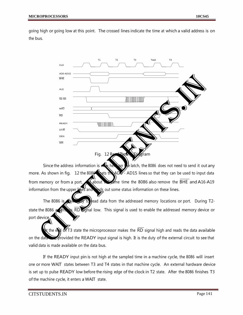
MICROPROCESSORS 10CS45
CITSTUDENTS.IN
Page 141
going high or going low at this point.
the bus.
The crossed lines indicate the time at which a valid address is on
T1 T2 T3 Twait T4
CLK
AD0-AD15
BHE
ALE
S2-S0
M/IO
RD
READY
DT/R
DEN
WR
Fig. 12 Read Timing Diagram
Since the address information is now held on the latch, the 8086 does not need to send it out any
more. As shown in fig. 12 the 8086 floats the AD0 - AD15 lines so that they can be used to input data
from memory or from a port. At about the same time the 8086 also remove the BHE and A16-A19
information from the upper lines and sends out some status information on these lines.
The 8086 is now ready to read data from the addressed memory locations or port. During T2-
state the 8086 asserts its RD signal low.
port device.
This signal is used to enable the addressed memory device or
At the end of T3 state the microprocessor makes the RD signal high and reads the data available
on the data bus, provided the READY input signal is high. It is the duty of the external circuit to see that
valid data is made available on the data bus.
If the READY input pin is not high at the sampled time in a machine cycle, the 8086 will insert
one or more WAIT states between T3 and T4 states in that machine cycle. An external hardware device
is set up to pulse READY low before the rising edge of the clock in T2 state.
of the machine cycle, it enters a WAIT state.
After the 8086 finishes T3
CITSTUDENTS.IN

MICROPROCESSORS 10CS45
CITSTUDENTS.IN
Page 142
If the READY input is still low at the end of a WAIT state, then the 8086 will insert another
WAIT state. The 8086 will continue inserting WAIT states until the READY input is sampled high
again.
If the
READY
input
is sampled
high
again
during T3 or
during
the
WAIT
state,
the
microprocessor comes out of the WAIT state and will initiate T4 of the machine cycle.
The DEN signal is used to enable bi-directional buffers on the data bus. The data enable signal,
DEN, from the 8086 will enable the data buffer when it is asserted LOW. The data transmit / receive
signal DT/ R from the 8086 is used to specify the direction in which the buffers are enabled. When DT/
R is asserted high, the buffers will, if enabled by DEN, transmit data from the 8086 to Memory or I/O
ports. When DT/ R is asserted low, the buffers, if enabled by DEN, will allow data to be received from
Memory or I/O ports of the 8086. DT/ R is asserted during T1 of the machine cycle. The DEN is
asserted after the 8086 finishes using the data bus to send the lower 16 address bits.
6.3 BUS Write Machine Cycle
The 8086 write operation is very similar to the read cycle. During T1 of a write machine cycle the
8086 asserts M/ IO low if the write is going to a port and it asserts M/ IO high if the write is going to
memory.
At about the same time the 8086 raises ALE
high to enable the address latches. The 8086 then assert BHE and on the lines AD0 - AD19, it output the
address that it will be writing to. When writing to a port, line A16 - A19 will always be low, because the
8086 only sends out 16-bits port addresses. The 8086 brings ALE low again to latch the address on the
outputs of the latches. In addition to holding the address, the latches also function as buffers for the
address lines.
After the address information is latched, the 8086 remove the address information from
AD0 - AD15 and outputs the desired data on these lines.
CITSTUDENTS.IN

MICROPROCESSORS 10CS45
CITSTUDENTS.IN
Page 143
Fig 13 Write Timing Diagram
If the READY input is sampled LOW by the 8086 before or during T2 of the machine cycle, the
8086 will insert a WAIT state after T3. If the READY input is sampled high before the end of the WAIT
state, the 8086 will go on with state T4 as soon as it completes the WAIT state. The 8086 will continue to
insect wait states for as long
as the READY is sampled low just before the end of each WAIT state.
6.3.1 Comparison of 8086 with the 8088 Microprocessor
The 8088 CPU is an 8-bit processor designed around the 8086 internal structure.
Most internal
functions of the 8088 are identical to the equivalent 8086 functions. The 8088 handles the external bus
the same way the 8086 does, one
difference
being
hat the
8088 handles only 8-bits at a time. 16-bit operands are fetched or written in two
AD0-AD7(8)
+5V
Gnd(2)
NMI
INTR
Clk
SSo (High)
MN/MX
RD
HOLD (RG/GT0)
A8-A15(8)
A16/S3(4)
A19/S6
Test
Ready
Reset
8088
HLDA (RQ/GT1)
WR (LOCK)
IO/M (S2)
DT/R(S1)
DEN (S0)
ALE (QS0)
INTA (QS1)
Fig . 14 Pin Configuration of 8088 Microprocessor
CITSTUDENTS.IN
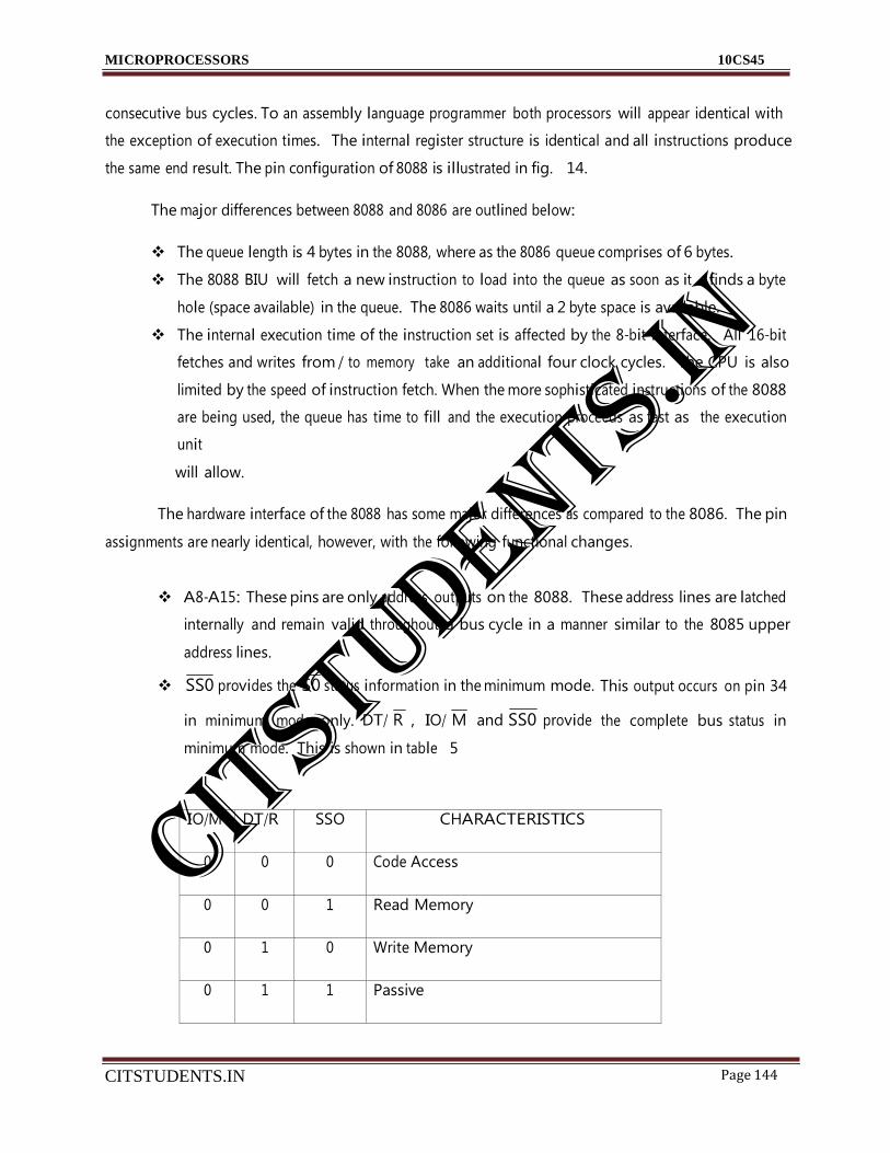
MICROPROCESSORS 10CS45
CITSTUDENTS.IN
Page 144
consecutive bus cycles. To an assembly language programmer both processors will appear identical with
the exception of execution times. The internal register structure is identical and all instructions produce
the same end result. The pin configuration of 8088 is illustrated in fig.
14.
The major differences between 8088 and 8086 are outlined below:
The queue length is 4 bytes in the 8088, where as the 8086 queue comprises of 6 bytes.
The 8088 BIU will fetch a new instruction to load into the queue as soon as it finds a byte
hole (space available) in the queue. The 8086 waits until a 2 byte space is available.
The internal execution time of the instruction set is affected by the 8-bit interface.
All 16-bit
fetches and writes from / to memory take an additional four clock cycles. The CPU is also
limited by the speed of instruction fetch. When the more sophisticated instructions of the 8088
are being used, the queue has time to fill and the execution proceeds as fast as
unit
will allow.
the execution
The hardware interface of the 8088 has some major differences as compared to the 8086.
assignments are nearly identical, however, with the following functional changes.
The pin
A8-A15: These pins are only address outputs on the 8088. These address lines are latched
internally and remain valid throughout a bus cycle in a manner similar to the 8085 upper
address lines.
SS0 provides the S0 status information in the minimum mode. This output occurs on pin 34
in minimum mode only. DT/ R , IO/ M and SS0 provide the complete bus status in
minimum mode. This is shown in table 5
IO/M DT/R SSO CHARACTERISTICS
0 0 0 Code Access
0 0 1 Read Memory
0 1 0 Write Memory
0 1 1 Passive
CITSTUDENTS.IN

MICROPROCESSORS 10CS45
CITSTUDENTS.IN
Page 145
1 0 0 Interrupt Acknowledge
1 0 1 Read I/O port
1 1 0 Write I/O port
1 1 1 Halt
Table 5
BHE has no meaning on the 8088 and has been eliminated.
IO/ M has been inverted. i.e., (In 8086, this pin as IO /M)
ALE is delayed by one clock cycle in the minimum mode when entering
HALT to allow the status to be latched with ALE.
Fig 15 illustrates the 8088 microprocessor system configuration. The Address-Data lines AD0-
AD7 are connected to the 74LS373 latch. The address from the multiplexed bus is latched into the
74LS373 when an ALE (Address latch enable) is active during T1 state of the microprocessor. The
address A0-A7 is available on the output of 74LS373 and can be used for memory (along with A16-A19),
and I/O devices. The address lines A8-A15 are not multiplexed with data lines or status lines, hence there
is no need to latch these address lines.
74LS245 is controlled by DT/ R and DEN
The data bus is connected to the 74LS245 transceiver. The
to transmit and receive and Data respectively.
chips.
lines.
Since 74LS373 and 74LS245 are also buffered chips, it is not required to add buffers to these
The address lines A8-A15 need to be buffered and hence the 74LS 244 buffer is used for these
The output of 74LS244 is always enabled.
CITSTUDENTS.IN

MICROPROCESSORS 10CS45
CITSTUDENTS.IN Page 146
A19/S6 - A16/S3 OE
A19 - A16
ALE
A15 - A8
74LS373 G
74LS
244
8088
AD0 - AD7
= OE
OE
G A0 - A7
74LS373
DT/R DEN
D0 - D7
74LS244
G D/R
Fig. 15
CITSTUDENTS.IN

MICROPROCESSORS 10CS45
CITSTUDENTS.IN Page 147
Why Decode Memory?
UNIT -7
When the 8088 microprocessor is compared to the 2716 EPROM, a difference in the number of
address connections surfaces-the EPROM has 11 address connections and the microprocessor
has 20. This means that the microprocessor sends out a 20-bit memory address whenever it reads
or writes data. Since the EPROM has only 11 address inputs, there is a mismatch that must
somehow be corrected. If only 11 of the 8088's address pins are connected to the memory, then
the 8088 will see only 2K bytes of memory instead of the 1M byte that it "expects" the memory
to contain. The decoder corrects the mismatch by decoding the address pins that do not connect
to the memory component.
The 3-to-8 Line Decoder (74LS138)
One of the more common, although not only, integrated circuit decoders found in many micro
processor-based systems is the 74LS138 3-to-8 line decoder. Figure 9-13 illustrates this decoder
and its truth table.
The truth table shows that only one of the eight outputs ever goes low at any time. For any
of the decoder's outputs to go low, the three enable inputs (G2A, G2B, and Gl) must all be ac
tive. To be active, the G2A and G2B inputs must both be low (logic 0), and G I must be high
(logic 1). Once the 74LS138 is enabled, the address inputs (C, B, and A) select which output pin
goes low. Imagine eight EPROM CE inputs connected to the eight outputs of the decoder! This
is a very powerful device because it selects eight different memory devices at the same time.
Selection { Input
Enable { Input
A 0
B I
c 2
74LSI3H 3 4
· G2A 5
G2B 6
Gl 7
Outputs
CITSTUDENTS.IN

CITSTUDENTS.IN Page 148
Input Outputs
Enable Select
en""A G2B Gl1 C B A () I 2 3 4 5 6 7
I X X X X X 1 1 1 1 ] 1 l I
X 1 X X X X 1 J 1 1 ] 1 1 1
X X () X X X 1 1 l l 1 I I I
0 0 I () () 0 0 I I I I I I I
() 0 I 0 () I I () I I I I I 1
() 0 I () I () I I 0 I l I l I
() () I () I I 1 I I 0 l 1 I I
0 () I I 0 0 I I I I () I I l
() 0 I I () I I I I l 1 0 I
0 0 I I I 0 I l I I l I 0 I
() 0 I I I l I I I I I l ] 0
'
Sample Decoder Circuit. Notice that the outputs of the decoder illustrated in Figure 9-14 are
connected to eight different 2764 EPROM memory devices. Here the decoder selects eight 8K
byte blocks of memory for a total of 64K bytes of memory. This figure also illustrates the ad
dress range of each memory device and the common connections to the memory devices. Notice
that all of the address connections from the 8088 are connected to this circuit. Also notice that
the decoder's outputs are connected to the CE inputs of the EPROMs, and the RD signal from
the 8088 is connected to the OE inputs of the EPROMs. This allows only the selected EPROM
to be enabled and to send its data to the microprocessor through the data bus whenever RD be
comes a logic 0.
In this circuit, a 3-input NAND gate is connected to address bits A 19-A 17. When all three
address inputs are high, the output of this NAND gate goes low and enables input G2B of the
74LS138. Input Gl is connected directly to A 16. In other words, in order to enable this decoder,
the first four address connections (A 19-A 16) must all be high.
CITSTUDENTS.IN

CITSTUDENTS.IN Page 149
t /
Atkin -.
Au - 1--
A, f-
Oo 27n4 1--
Data t f-
" 07 t--
RD OE
A () FOOOO - F I FFF
CE
13 I F20000 · FJFFF
CE
c 2
F4000 • F.'iFFF "'CE
F6000 • F7FFF CE
-
:b-
G2A
r 'I X
4 FXOOO • FYFFF
..J CE FAOOO • FRFFF
G2B 5
6 FCOOO - FDFFF
.:;l CE
t\ '" Gl CE
7 FEOOO · FFFFF
..J CE
FIGURE 9-14 A circuit that uses eight 2764 EPROMs for a 64K x 8 section of memory in an
8088 microprocessor-based system. The addresses selected in this circuit are
FOOOOH-FFFFFH.
The Dual 2-to-4 Line Decoder (74LS139)
Another decoder that finds some application is the 74LS139 dual 2-to-4line decoder. Figure 9-15
illustrates both the pin-out and the truth table for this decoder. The 74LS139 contains two sepa
rate 2-to-4 line decoders--each with its own address, enable, and output connections.
74 LS 139
Selection J mpuh \
Enahlc
in rut
Scle,·tion I mruh
Enahlc
input
1/\ IY.,
IH IY 1
IY
IE IY,
r-------- '2A 2Yo
'28 2Y 1
2Y,
2E 2Y,
Outpuh
Outpuh CIT
STUDENTS.IN

CITSTUDENTS.IN Page 150
MICROPROCr"""" "
10CS45 Input Outputs
IT
A
B - Yn Y,
y2
YJ
0
0
0
0
I
I
I
0
()
I
I
0
I
I
0
I
0
I
I
0
I
()
I
I
I
I
I
0
I
X
X
I
I
I
I
PLD Programmable Decoders
This section of the text explains the use of the programmable logic device or PLD as a decoder.
Recently, the PAL has replaced PROM address decoders in the latest memory interfaces. There
are three PLD devices that function in basically the same manner, but have different names: PLA
(programmable logic array), PAL (programmable array logic), and GAL (gated array
logic). Although these devices have been in existence since the mid-1970s, they have only re
cently appeared in memory systems and digital designs. The PAL and the PLA are fuse pro
grammed, as is the PROM, and some PLD devices are erasable, as are EPROMs. In essence, all
three devices are arrays of logic elements that are programmable.
Combinatorial Programmable Logic Arrays. One of the two basic types of PALs is the combina
torial programmable logic array. This device is internally structured as a programmable array of
combinational logic circuits. Figure 9-17 illustrates the internal structure of the PAL l6L8 that is
constructed with AND/OR gate logic. This device, which is very common, has 10 fixed inputs,
2 fixed outputs, and 6 pins that are programmable as inputs or outputs. Each output pin is gener
ated from a 7-input OR gate that has an AND gate attached to each input. The outputs of the OR
gates pass through a three-state inverter that defines each out as an AND/NOR function. Ini
tially, all of the fuses connect all of the vertical/horizontal connections illustrated in Figure 9-17.
Programming is accomplished by blowing fuses to connect various inputs to the OR gate array.
The wired-AND function is performed at each input connection that allows a product term of up
to 16 inputs. A logic expression using the PAL16L8 can have 7 product terms with 16 inputs
NORed together to generate the output expression. This device is ideal as a memory address de
coder because of its structure. It is also ideal because the outputs are active low. CITSTUDENTS.IN

CITSTUDENTS.IN Page 151
t
Interfacing EPROM to the 8088. You will find this section very similar to Section 9-2 on de
coders. The only difference is that, in this section, we discuss wait states and the use of the IO/M
signal to enable the decoder.
Figure 9-19 illustrates an 8088 microprocessor connected to eight 2732 EPROMs, 4K x 8
memory devices that are in very common use today. The 2732 has one more address input (A 11)
than the 2716, and twice the memory. The device in this illustration decodes eight 4K x 8 blocks
of memory, for a total of 32K x 8 bits of the physical address space for the 8088.
The decoder (74LS138) is connected a little differently than might be expected because the
slower version of this type of EPROM has a memory access time of 450 ns. Recall from Chapter
8 that when the 8088 is operated with a 5 MHz clock, it allows 460 ns for the memory to access
data. Because of the decoder's added time delay (12 ns), it is impossible for this memory to func
tion within 460 ns. In order to correct this problem, we must add a NAND gate to generate a
signal to enable the decoder and a signal for the wait state generator, covered in Chapter 8. (Note
that the 80188 can internally insert .from 0-15 wait states without any additional external hard
ware, so it does not require this NAND gate.) With a wait state inserted every time this section of
the memory is accessed, the 8088 will allow 660 ns for the EPROM to access data. Recall that an
extra wait state adds 200 ns (1 clock) to the access time. The 660 ns is ample time for a 450 ns
memory component to access data, even with the delays introduced by the decoder and any
buffers added to the data bus.
Notice that the decoder is selected for a memory address range that begins at location
F8000H and continues through location FFFFFH-the upper 32K bytes of memory. This section
of memory is an EPROM because FFFFOH is where the 8088 starts to execute instructions after
a hardware reset. We often call location FFFFOH the cold-start location. The software stored in
this section of memory would contain a JMP instruction at location FFFFOH that jumps to loca
tion F8000H so that the remainder of the program can execute.
1\ddn:: :-. > t -
A, f-
-- v A,. r- o, 2732
Data
o,
r-
- ,.....
A• .:- A 0
F!{000-F8FFF
CE A,. B F9000-F9FFF
2 FAOOO-FAFFF
CE
10/M -p ·ux :l CE FCOOO-FCFFF
A.;;- 4 CE
A,t , - >-------<: G2A 5 FDOOO-FDFFF
CE
A, , - .;;\. G2B 6 FEOOO-FEFFF
CE A,,- FFOOO-FFFFF A •.,
F Gl 7 CE
I IK
+5V
FIGURE 9-19 Eight 2732 EPROMs interfaced to the 8088 microprocessor. Note that the output of the NAND gate is used to cause a wait state whenever this section of the memory is selected.
CITSTUDENTS.IN

CITSTUDENTS.IN Page 152
MICROPROCESSORS 10CS45
Interfacing RAM to the 8088. RAM is a little easier to interface than EPROM because most
RAM memory components do not require wait states. An ideal section of the memory for the
RAM is the very bottom, which contains vectors for interrupts. Interrupt vectors (discussed in
more detail in Chapter 11) are often modified by software packages, so it is rather important to
encode this section of the memory with RAM.
In Figure 9-20, sixteen 62256 32K x 8 static RAMS are interfaced to the 8088, beginning
at memory location OOOOOH. This circuit board uses two decoders to select the sixteen different RAM memory components and a third to select the other decoders for t)le appropriate memory
sections. Sixteen 32K RAMs fill memory from location OOOOOH through location 7FFFFH, for
512K bytes of memory.
The first decoder (U4) in this circuit selects the other two decoders. An address beginning with
00 :-- elects decoder U3, and an address that begins with 0 I selects decoder U9. Notice that extra pins
remain at the output of decoder U4 for future expansion. These allow more 256K x 8 blocks of
RAM, for a total of l M x 8, simply by adding the RAM and the additional secondary decoders.
Also notice from the circuit in Figure 9-20 that all the address inputs to this section of
memory are buffered, as are the data bus connections and control signals RD and WR. Buffering
is important when many devices appear on a single board or in a single system. Suppose that
three other boards like this are plugged into a system. Without the buffers on each board, the load
on the system address, data, and control buses would be enough to prevent proper operation.
(Excessive loading causes the logic 0 output to rise above the 0.8 V maximum allowed in a
system.) Buffers are normally used if the memory will contain additions at some future date. If
the memory will never grow, then buffers may not be needed.
Interfacing Flash Memory
Flash memory (EEPROM) is becoming commonplace for storing setup information on video
cards as well as for storing the system BIOS in the personal computer. Flash memory is also
found in many other applications to store information that is only changed occasionally.
The only difference between a flash memory device and SRAM is that the flash memory
device requires a 12 V programming voltage to erase and write new data. The 12 V can either be
available at the power supply, or a 5 V-to-12 V converter designed for use with flash memory
can be obtained.
CITSTUDENTS.IN

CITSTUDENTS.IN Page 153
? -+ 1A4
1Y2
r
3: 14
1
- 01
6
U7A
::E Y5
9
B c
Y1
A
U1
1A1
A2 --i 1A2
A3 :::;J: 1A3
1Y1 ....!!.../
1Y3 j,_,· 1Y4
Bank O
AS 11 A6 A7
D, b,
2A1 2A2 2A3 2A4
g
2Y1 -f-', 2Y2 -
=u
-=- '- 7-4L-S2-44---'
U2
i2 1A1
A10 lA2 A11 lA3 A12 11 l A4
A13 A14 1 2A3
7 2A4
AO ±
1Y2 1Y3 1Y4 2Y1 2Y2 2Y3 2Y4
,_ _ o01o
:/::- 02 ;c-03 ;c-04 ;c-OS ;r--o6 ;r--o7
62256
U3
WA -4.- 1A1 1A2 1A3
-J.J. 1A4 U3
A15 A16 2A1 1
2A2 A A17 2A3
_!L 2A4
YO Y1 Y2 12 Y3 11
.o1±; g
4 G1
G2A
Y4 1
Y5 9
":" . . . 74LS24_4_.J G2B 7 cs
74LS138 I cs
U4
A18 A A19 B
YO l:>tf- c Y2 b.J4..-
Y3 1 L G1 0
" : 4 g_0_6..J 74LS13S I
Bank 1
A1 .- A2 A3 .- A4 AS .- A6
DO A1
us
A7 .._- AS .- A9 A10
.._- A11
01 --¥- A2 B21 E A12
023 4 A4
B3 .._- A13
04 AS OS A6
06 --4- A7 07 ---'!..- AS
,.-lf< G
BS 44 5 4 21
BS 1 USA
=rr:::l
- A14
'- - oo
-... ==g '- f--- 04
62256
DIA 74LS20 74LS245
l' f--- 05
L.-------- --4 +44----------- I , 07
2
74LSOO
USA
JO/M 1 2
'-----< WE
OE
,---- - - -Q cs
cs U9
1 .----- - - d cs
2 B Y1 14 I cs
74LS04 3 c Y2 2 I Y3 11 cs
6 G1 Y4 10
cs G2A
G2B 7 cs
74LS13S I
cs
FIGURE 9-20 A 512K byte static memory system using 16 62255 SRAMS
CITSTUDENTS.IN

CITSTUDENTS.IN Page 154
s r
42 D09
A10 D011 ..--
34
VPP
,
AO
U? :B
BYTE DOO DO
A1 11
AO D01 D1
A2 9 A3 8 A4
A1 D02 D2 A2 D03 D3 A3 D04 D4
AS 6 A4 DOS
?R DS
A6 AS A7 A6
D06 D6 DO?
1 D7
AS 4
A? DOS A9 41 AS
A10 A11
A12
40 A9 D010
39
A12 D013
A13 A14 A15 A16 A17 A1S
A19
sA11 D012 !--
37 A13 D014 36 A14 D01S 35 A15
3 A16
U?A A17
A YOpt-- RD 1A
OE ,_-----2 B Y1 4 CE
Y2 WR 44 WE
IOiM1-r--1- G Y3 .---1-
PWD 74LS139
2SF400
PWRDN
VPP
FIGURE 9-21 The 28F400 flash memory device interfaced to the 8088 microprocessor
8086, 80186, 80286, AND 80386SX (16-BIT) MEMORY INTERFACE
16-Bit Bus Control
The data bus of the 8086, 80186, 80286, and 80386SX is twice as wide as the bus for the
8088/80188. This wider data bus presents us with a unique set of problems that have not been en
countered before. The 8086, 80186, 80286, and 80386SX must be able to write data to any 16-
bit location--or any 8-bit location. This mea,ns that the 16-bit data bus must be divided into two
separate sections (banks) that are 8-bits wide so the microprocessor can write to either half (8-
bit) or both halves (16-bit). Figure 9-26 illustrates the two banks of the memory. One bank (low
bank) holds all the even-numbered memory locations, and the other bank (high bank) holds all
the odd-numbered memory locations.
The 8086, 80186, 80286, and 80386SX use the BHE signal (high bank) and the A0 address
bit or BLE (bus low enable) to select one or both banks of memory used for the data transfer.
Table 9-3 depicts the logic levels on these two pins and the bank or banks selected.
Bank selection is accomplished in two ways: (1) a separate write signal is developed to se
lect a write to each bank of the memory or (2) separate decoders are used for each bank. As a
careful comparison reveals, the first technique is by far the least costly approach to memory in
terface for the 8086, 80186, 80286, and 80386SX microprocessors.
CITSTUDENTS.IN

CITSTUDENTS.IN Page 155
MICROPROCESSORS 10CS45
`
CITSTUDENTS.IN

CITSTUDENTS.IN Page 156
2 8 f--
-=
g1: s
J s
3 c Y2 13
+
8
D9-D15
DO·D7
A1-A16
H1gh bank
vee -
64K x 8
'-- DO·D7 - < r--
U1 1--
A20 1 A YO PB-- AO-A15
A21 Y1
A22 3 c Y2 PW- Y3
1--
Y4 ,.--- G1 YS
A23 4 G2A Y6 rC rG28 Y7
.-ds 74LS138
A18
r-ds U2
Y1 I s
A17 1 A YO 15
2 14
Y3 r s
A19 3 c Y2 13
6 Y4
lll_
0 G1 YS Iii* 4
G2A Y6 9
P< G2B Y7 7
74LS138
Low bank
f--
64K X B
-
D0-07 r--
1--
f--
AO·A15 - 1--
,c s
.-ds
U3
c-4-- A YO 15
s
2 8 Y1 14 ,...ds
Y3 12
Y4 11
G1 YS 1
I _rLs 4 G2A Y6 9 .-Js
..2.c G2B Y7 7 s
74LS138
FIGURE 9-27 Separate bank decoders
Isolated and Memory-Mapped 1/0
There are two completely different methods of interfacing 110 to the microprocessor: isolated
110 and memory-mapped 110. In isolated 110, the IN, INS, OUT, and OUTS instructions
transfer data between the microprocessor accumulator or memory and the 110 device. In
memory-mapped 110, any instruction that references memory can accomplish the transfer. Both
isolated and memory-mapped 110 are in use, so both are discussed in this text
Isolated 1/0. The most common 110 transfer technique used in the Intel microprocessor-based
system is isolated 110. The term isolated describes how the 110 locations are isolated from the
CITSTUDENTS.IN
CITSTUDENTS.IN Page 157
memory system in a separate 110 address space. (Figure 10-1 illustrates both the isolated and
CITSTUDENTS.IN

CITSTUDENTS.IN Page 157
.. .,.........,,...,,...,,...,.,...,,...,.......,"'1"':1................
FIGURE 10-1 The memory Memory
and 1/0 maps for the 8086/ FFFFF
8088 microprocessors.
(a) Isolated 1/0 (b) Memory-
mapped 1/0
IM x 8 FFFF 110
64K X 8
()()000 0000
(a)
FFFFF Memory + 1/0
110
00000 L------
(b)
CITSTUDENTS.IN

CITSTUDENTS.IN Page 158
memory-mappec(actdresss \cesfor any Intel 80X86 or Pentium microprocessor.) The addresses
for isolated 1/0 devices, called ports, are separate from the memory. As a result, the user can ex
pand the memory to its full size without using any of this space for 1/0 devices. A disadvantage
of isolated I/0 is that the data transferred between I/0 and the microprocessor must be accessed
by the IN, INS, OUT, and OUTS instructions. Separate control signals for the I/0 space are de
veloped (using M/10 and W/R) that indicate an I/0 read (IORC) or an 1/0 write (IOWC) opera
tion. These signals indicate that an I/0 port address appears on the address bus that is used to
select the I/0 device. In the personal computer, isolated I/0 ports are used for controlling pe
ripheral devices. As a rule, an 8-bit port address is used to access devices located on the system
board. such as the timer and keyboard interface. while a 16-bit port is used to access serial and
parallel ports as well as video and disk drive systems.
Memory-Mapped 1/0. Unlike isolated 1/0, memory-mapped I/0 does not use the IN, INS,
OUT, or OUTS instructions. Instead, it uses any instruction that transfers data between the mi
croprocessor and memory. A memory-mapped I/0 device is treated as a memory location in the
memory map. The main advantage of memory-mapped 1/0 is that any memory transfer instruc
tion can be used to access the 1/0 device. The main disadvantage is that a portion of the memory
system is used as the 1/0 map. This reduces the amount of memory available to applications. An
other advantage is that the IORC and IOWC signals have no function in a memory-mapped l/0
system and may reduce the amount of circuitry required for decoding.
FIGURE 10-1 The memory
and 1/0 maps for the 8086/
8088 microprocessors.
(a) Isolated 1/0 {b) Memory
mapped 1/0
Memory FFFFF ..---------,
IM X 8
110 FFFF ..---------,
64K X 8
00000 1.....------' 0000 1.....------'
( a)
FFFFF Memory+ 1/0
110
00000 .._ _.
(b)
CITSTUDENTS.IN

CITSTUDENTS.IN Page 159
c
FIGURE 1()-6 A port de
coder that decodes 8-bit 1/0 AO Ul
A YO FOH
ports. This decoder generates AI A2
active low outputs for ports
FOH-F7H. A4 A3
B Yl Y2 Y3 Y4
GJ YS G2A Y6
FIH F2H F3H F4H FSH F6H
U2A AS A6 A7
74LSIO
G2B Y7 F7H
74ALSJ38
decoder. Figure 10-7 shows the PAL version of this decoder. Notice that this is a better decoder
circuit because the number of integrated circuits has been reduced to one device, the PAL. The
program for the PAL appears in Example 10-2.
1/0 PORT ADDRESS DECODING
1/0 port address decoding is very similar to memory address decoding, especially for memory
mapped 1/0 devices. In fact, we do not discuss memory-mapped 1/0 decoding because it is
treated exactly the same as memory, except that the IORC and IOWC are not used, since there is
no IN or OUT instruction. The decision to use memory-mapped I/0 is often determined by the
size of the memory system and the placement of the I/0 devices in the system.
The main difference between memory decoding and isolated 1/0 decoding is the number of
address pins connected to the decoder. We decode A 32-A0, A23-A0, or A 19-A0 for memory and
A 15-A0 for isolated I/0. Sometimes, if the I/0 devices use only fixed I/0 addressing, we decode
only A7-A0. Another difference is that we use the IORC and IOWC to activate l/0 devices for a
read or a write operation. On earlier versions of the microprocessor, 10/M = 1 and RD or WR are
used to activate l/0 devices. On the newest versions of the microprocessor, the M/10 = 0 and W!R are used to activate 1/0 devices.
Decoding 8-Bit 1/0 Addresses
As mentioned, the fixed l/0 instruction uses an 8-bit l/0 port address that appears on A 15-A0 as
OOOOH-OOFFH. If a system will never contain more than 256 I/0 devices, we often decode only ad
dress connections A7-A0 for an 8-bit 1/0 port address. Thus, we ignore address connections A 15-A8•
(You cannot ignore these address connections in a personal computer-all 16 bits must be used.)
Please note that the DX register can also address I/0 ports OOH-FFH. Also note that if the address is
decoded as an 8-bit address, then we can never include 1/0 devices that use a 16-bit l/0 address.
Figure 10-6 illustrates a 74ALS138 decoder that decodes 8-bit 1/0 ports FOH-F7H. (We
assume that the system will only use I/0 ports OOH-FFH for this decoder.) This decoder is iden
tical to a memory address decoder except we only connect address bits A7-A0 to the inputs of the
!!
CITSTUDENTS.IN

CITSTUDENTS.IN Page 160
FIGURE 1Q-7 A PAL16L8
decoder that generates 1/0
port signals for port FOH-F7H
UI
AO AI A2 A3 A4 A5 A6 A7
16L8
FIGURE 10-8 A PAL16L8
decoder that decodes 16-bit
address EFF8H-EFFFH
A12
U1A
FF8
EFF9 EFFA EFFB EFFC
A15-------*l
j-------- --
: J-------cms A9------ 1*1 AS -------- - '1-2"' 74LS30
EFFO EFFE EFFF
address lines (A 15-A8) must be decoded. Figure 10-8 illustrates a circuit that contains a
PAL16L8 and an 8-input NAND gate used to decode 1/0 ports EFF8H-EFFFH. These are
common l/0 port assignments in a PC used for the serial communications port.
The NAND gate decodes the first 8-bits of the 1/0 port address (A 15-A8) so that it gener
ates a signal to enable the PAL16L8 for any 1/0 address between EFOOH and EFFFH. The
PAL16L8 further decodes the 1/0 address to produce eight active low output strobes EFF8H
EFFFH. The program for the PAL16L8 appears in Example 10-3.
CITSTUDENTS.IN

MICROPROCESSORS 10CS45
CITSTUDENTS.IN
Page 161
Unit-8
8.1 Interrupt Driver I/O
A disadvantage of conditional programmed I/O is that the microcomputer needs to check the status bit
(BUSY signal for the A/D converter) by waiting in a loop. This type of I/O transfer is dependent on the
speed of the external device. For a slow device, this waiting may slow down the capability of the
microprocessor to process other data. The interrupt I/O technique is efficient in this type of situation.
Interrupt I/O is a device-initiated I/O transfer. The external device is connected to a pin called the
interrupt (INT) pin on the processor chip. When the device needs an I/O transfer with the microcomputer,
it activates the interrupt pin of the processor chip. The microcomputer usually completes the current
instruction and saves at least the contents of the current program counter on the stack.
The microcomputer then automatically loads an address into the program counter to branch to a
subroutine like program called the interrupt service routine. This program is written by the user. The
external device wants the microcomputer to execute this program to transfer data. The last instruction of
the service routine is a RETURN, which is typically the same instruction used at the end of a subroutine.
This instruction normally loads the address (saved in the stack before going to the service routine) in the
program counter. Then, the microcomputer continues executing the main program.
8.1.1 Interrupt Types:
There are typically three types of interrupts : external interrupts, traps or internal interrupts, and
software interrupts.
External interrupts are initiated through the microcomputer’s interrupt pins by external devices such as
A/D converters. A simple example of an external interrupt was given in the previous section.
External interrupts can further be divided into two types: maskable and nonmaskable. A maskable
interrupt is enabled or disabled by executing instructions such as EI or DI. If the microcomputer’s
interrupt is disabled, the microcomputer ignores the maskable interrupt. Some processors, such as the
Intel 8086, have an interrupt flag bit in the processor status register. When the interrupt is disabled, the
interrupt flat bit is 1, so no maskable interrupts are recognized by the processor.
resets to zero when the interrupt is enabled.
The interrupt flag bit
CITSTUDENTS.IN

MICROPROCESSORS 10CS45
CITSTUDENTS.IN
Page 162
The nonmaskable interrupt has higher priority than the maskable interrupt. If both maskable and
nonmaskable
interrupt first.
interrupts are activated at the same time, the processor will service the nonmaskable
Internal interrupts, or traps, are activated internally by exceptional conditions such as overflow, division
by zero, or execution of an illegal op-code. Traps are handled the
same way as external interrupts. The user writes a service routine to take corrective measures and provide
an indication to inform the user that an exceptional condition has occurred.
Many processors include software interrupts, or system calls. When one of these instructions is executed,
the processor is interrupted and serviced similarly to external or internal interrupts. Software interrupt
instructions are normally used to call the operating system. Software interrupt instructions allow the user
to switch from user to supervisor mode.
8.1.2 Interrupt Address Vector:
The technique used to find the starting address of the service routine (commonly known as the interrupt
address vector) varies from one processor to another. With some processors, the manufacturers define the
fixed starting address for each interrupt. Other manufacturers use an indirect approach by defining fixed
locations where the interrupt address vector is stored.
8.1.3 Saving the Microprocessor Registers:
When a processor is interrupted, it saves at least the program counter on the stack so tae processor can
return to the main program after executing the service routine. Some processors save only one or two
registers, such as the program counter and status register. Other processors save all microprocessor
registers before going to the service routine.
saves prior to executing the service routine.
The user should know the specific registers the processor
This will enable the user to use the appropriate return
instruction at the end of the service routine to restore the original conditions upon return to the main
program.
CITSTUDENTS.IN

MICROPROCESSORS 10CS45
CITSTUDENTS.IN
Page 163
8.1.4 Interrupt Priorities:
A processor is typically provided with one or more interrupt pins on the chip. Therefore, a special
mechanism is necessary to handle interrupts from several devices that share on of these interrupt lines.
There are two ways of servicing multiple interrupts: polled and daisy chain techniques.
Polled interrupts are handled by software and therefore are slower when compared with daisy chaining.
The processor responds to an interrupt by executing one general service routine for all devices. The
priorities of devices are determined by the order in which the routine polls each device. The processor
checks the status of each device in the general service routine, starting with the highest priority device to
service an interrupt. Once the processor determines the source of the interrupt, it branches to the service
routine for the device.
In a daisy chain priority system, devices are connected in a daisy chain fashion to set up a priority system.
Suppose one or more devices interrupt the processor. In response, the
processor pushes at lease the PC and generates an interrupt acknowledge (INTA) signal to the highest
priority device. If this device has generated the interrupt, it will accept the INTA. Otherwise, it will pass
the INTA onto the next device until INTA is accepted. Once accepted, the device provides a means for
the processor to find an interrupt address vector by using external hardware. The daisy chain priority
scheme is based on mostly hardware and is therefore faster than the polled interrupt.
8.1.5 Direct Memory Access (DMA)
Direct Memory Access (DMA) is a technique that transfers data between a microcomputer’s memory and
I/O device without involving the microprocessor. DMA is widely used in transferring large blocks of
data between a peripheral device and the microcomputer’s memory. The DMA technique uses a DMA
controller chip for the data transfer operation.
summarized as follows:
The main functions of a typical DMA controller are
• The I/O devices request DMA operation via the DMA request line of the controller chip.
• The controller chip activates the microprocessor HOLD pin, requesting the CPU to release
the bus.
• The processor sends HLDA (hold acknowledge) back to the DMA controller, indicating that
the bus is disabled. The DMA controller places the current value of its internal registers,
CITSTUDENTS.IN

MICROPROCESSORS 10CS45
CITSTUDENTS.IN
Page 164
such as the address register and counter, on the system bus and sends a DMA acknowledge to
the peripheral device. The DMA controller completes the DMA transfer.
There are three basic types of DMA: block transfer, cycle stealing, and interleaved DMA.
For block transfer DMA, the DMA controller chip takes the bus from the microcomputer to transfer data
between the memory and I/O device. The microprocessor has no access to the bus until the transfer is
completed. During this time, the microprocessor can perform internal operations that do not need the bus.
This method is popular with microprocessors. Using this technique, blocks of data can be transferred.
Data transfer between the microcomputer memory and an I/O device occurs on a word-by-word basis
with cycle stealing.
the system clock.
Typically, the microprocessor clock is enabled by ANDing an INHIBIT signal with
The system clock has the same frequency as the microprocessor clock. The DMA
controller controls the INHIBIT line. During normal operation, the INHIBIT line is HIGH, providing the
microprocessor clock. When DMA operation is desired, the controller makes the INHIBIT line LOW for
one clock cycle. The microprocessor is then stopped completely for the cycle. Data transfer between the
memory and I/O takes place during this cycle. This method is called cycle
stealing because the DMA controller takes away or steals a cycle without microprocessor recognition.
Data transfer takes place over a period of time.
With interleaved DMA, the DMA controller chip takes over the system bus when the microprocessor is
not using it. For example, the microprocessor does not use the bus while incrementing the program
counter or performing an ALU operation. The DMA controller chip identifies these cycles and allows
transfer of data between the memory and I/O device.
this method.
Data transfer takes place over a period for time for
8.2 Types of data transfer
Simple I/O – used when timings of I/O device is known
(Ex. Collect newspaper leisurely any time after 8 a.m.)
Status check I/O – Data transfer done anytime after I/O device says it is ready
CITSTUDENTS.IN

MICROPROCESSORS 10CS45
CITSTUDENTS.IN
Page 165
ITN Interrupt type
5 Out of bound(80286)
6 Invalid opcode
7 No Coprocessor
8 Double fault (during an
instruction 2 interrupts)
(Ex. Check newspaper box and collect newspaper if it is in the box)
Interrupt driven I/O – data transfer done immediately after I/O device interrupts
(Ex. Collect newspaper when the door bell rings indicating delivery of newspaper)
In this section only Interrupt driven I/O is discussed.
Interrupt driven I/O
Interrupt types
Hardware interrupts Software interrupts Exceptions or Traps
Ex. NMI and INTR pins Ex. INT n, INT 3, INTO
instructions
Ex. Divide by zero error,
Single step interrupt
Interrupt type numbers
Every interrupt type in 8086 has an 8-bit Interrupt type number (ITN) as shown below.
ITN Interrupt type
0 Divide by 0 error
1 Single step interrupt
2 NMI
3 Break point interrupt
4 Overflow error
CITSTUDENTS.IN

MICROPROCESSORS 10CS45
CITSTUDENTS.IN
Page 166
5 -1F Reserved by Intel. 20-FF Available for user.
13H for Disk services INT 21H for DOS services.
Action when NMI is activated
NMI is positive edge triggered input
1. Complete the instruction in progress
2. Push Flags on the stack
3. Reset IE flag (to ensure no further interrupts)
4. Reset T flag (so that interrupt service subroutine, ISS, is not executed in single step)
5. PUSH CS
6. PUSH IP
7. IP loaded from word location 2 x 4 = 8 (2 is ITN)
8. CS loaded from next word location (0000AH)
Processor makes a branch to the subroutine!
8.2.1 Interrupt Vector table (IVT)
RAM locations 0 to 003FFH are used to store IVT. It contains 256 Interrupt
Vectors (IV) each of 4 bytes.
00000H 1234H
00002H 5678H 5678:1234H is IV number 0
00004H 3344H
CITSTUDENTS.IN

MICROPROCESSORS 10CS45
CITSTUDENTS.IN
Page 167
5566H
:
6677H
7788H
00006H 5566:3344H is IV number 1
: :
003FCH
003FEH 7788:6677H is IV number FF
8.2.2 Execution of INT n (n=0 to FF)
1. Push Flags on the stack
2. Reset IE flag (to ensure no further interrupts)
3. Reset T flag (so that ISS is not executed in single step)
4. PUSH CS
5. PUSH IP
6. IP loaded from word location n x 4 = say, W
7. CS loaded from next word location W+2
In INT n, which is a 2-byte instruction, n is the ITN. INT n has the opcode CDH
Action when INT 3 is executed
1. Push Flags on the stack
2. Reset IE flag (to ensure no further interrupts)
3. Reset T flag (so that ISS is not executed in single step)
4. PUSH CS
5. PUSH IP
6. IP loaded from word location 3 x 4 = 0000CH
7. CS loaded from next word location 0000EH
INT 3 is a 1-byte instruction with opcode of CCH
CITSTUDENTS.IN

MICROPROCESSORS 10CS45
CITSTUDENTS.IN
Page 168
8.2.3 What is divide by 0 error?
Ex. DIV BL
Before After
AH 40H
AL 60H
BL 02H
00H 2030H
This is an example for divide by 0 error. It only
means quotient is too large for the register!
Action for divide by 0 error
For divide by 0 error the ITN is 0
1. Push Flags on the stack
2. Reset IE flag (to ensure no further interrupts)
3. Reset T flag (so that ISS is not executed in single step)
4. PUSH CS
5. PUSH IP
6. IP loaded from word location 0 x 4 = 00000H
7. CS loaded from next word location 00002H
Processor makes a branch to the subroutine at location 5678:1234H if the contents of IVT is as
shown in the table above.
Action for Single step interrupt
For divide by 0 error the ITN is 1
CITSTUDENTS.IN

MICROPROCESSORS 10CS45
CITSTUDENTS.IN
Page 169
1. Push Flags on the stack
2. Reset IE flag (to ensure no further interrupts)
3. Reset T flag (so that ISS is not executed in single step)
4. PUSH CS
5. PUSH IP
6. IP loaded from word location1 x 4 = 00004H
7. CS loaded from next word location 00006H
Processor makes a branch to the subroutine at location 5566:3344H as per the IVT
8.2.4 Action for INTO instruction
INTO is a 1-byte instruction. For interrupt on overflow the ITN is 4.
1. Do steps 2 to 7 only if Overflow flag is set
2. Push Flags on the stack
3. Reset IE flag and T flag
4. PUSH CS
5. PUSH IP
6. IP loaded from word location 4 x 4 = 00010H
7. CS loaded from next word location 00012H
INTO is equivalent to: JNO Next
INT 4
Next: ….
CITSTUDENTS.IN

MICROPROCESSORS 10CS45
CITSTUDENTS.IN
Page 170
Action when INTR is activated
INTR is level triggered input.
1. Complete the instruction in progress
2. Activate INTA o/p twice. In response 8086 receives ITN n instruction from an external device
like 8259 PIC
3. Push Flags on the stack. Reset IE and T flags
4. PUSH CS
5. PUSH IP
6. IP loaded from word location n x 4 = say, W
7. CS loaded from next word location W+2
Processor makes a branch to the subroutine!
8.2.5 IRET (Return from Interrupt) instruction
An ISS ends with the IRET instruction.
IRET is same as POP IP + POP CS + POPF
SP after branch to ISS
IP
CS
SP before branch to ISS FLAGS
Make sure ISS does not end with RET!
CITSTUDENTS.IN

MICROPROCESSORS 10CS45
CITSTUDENTS.IN
Page 171
8.2.6 Priority of 8086 Interrupts
If several interrupts occur during the execution of an instruction, in which order interrupts will be
serviced? There will be priorities as indicated below.
Divide by 0 error, INT n Highest priority
NMI
INTR
Single step interrupt Lowest priority
In reality NMI has highest priority! If NMI occurs during the servicing of INT n, processor
branches to NMI routine as IE flag has no effect on NMI.
CITSTUDENTS.IN

MICROPROCESSORS 10CS45
CITSTUDENTS.IN
Page 172
8.2.7 Intel 8255 PPI
PPI is abbreviation for Programmable Peripheral Interface. It is an I/O port chip used for interfacing I/O
devices with microprocessor. It is a very commonly used peripheral chip.
Knowledge of 8255 essential for students in the Microprocessors lab for interfacing experiments.
Vcc
8255 40 pin DIP
A7 Gnd
A6 RD*
A5 D7-0
A4 A1
Port A
Port C
Control Port
Port B
PA7-0 PC7-4
PC3-0
There are 3 ports in 8255 from user’s point of view - Port A, Port B and Port C.
Port C is composed of two independent 4-bit ports : PC7-4 (PC Upper) and PC3-0 (PC Lower)
Selection of Ports
A1 A0 Selected port
0 0 Port A
0 1 Port B
1 0 Port C
1 1 Control port
CITSTUDENTS.IN

MICROPROCESSORS 10CS45
CITSTUDENTS.IN
Page 173
There is also a Control port from the Processor point of view. Its contents decides the working of 8255.
When CS (Chip select) is 0, 8255 is selected for communication by the processor. The chip select circuit
connected to the CS pin assigns addresses to the ports of 8255.
For the chip select circuit shown, the chip is selected when A7=0, A6=1, A5=1, A4=1, A3=1, A2=1, and
M/IO*= 0. Port A, Port B, Port C and Control port will have the addresses as 7CH, 7DH, 7EH, and 7FH
respectively.
There are 3 modes of operation for the ports of 8255. Mode 0, Mode 1, and Mode 2.
Mode 0 Operation
It is Basic or Simple I/O. It does not use any handshake signals. It is used for interfacing an i/p device or
an o/p device. It is used when timing characteristics of I/O devices is well known.
Mode 1 Operation
It uses handshake I/O. 3 lines are used for handshaking. It is used for interfacing an i/p device or an o/p
device. Mode 1 operation is used when timing characteristics of I/O devices is not well known, or used
when I/O devices supply or receive data at irregular intervals.
Handshake signals of the port inform the processor that the data is available, data transfer complete etc.
More details about mode 1 operation is provided later.
Mode 2 Operation
It is bi-directional handshake I/O. Mode 2 operation uses 5 lines for handshaking. It is used with an I/O
device that receives data some times and sends data sometimes. Ex. Hard disk drive. Mode 2 operation is
useful when timing characteristics of I/O devices is not well known, or when I/O devices supply or
receive data at irregular intervals.
Port A can work in Mode 0, Mode 1, or Mode 2
Port B can work in Mode 0, or Mode 1
Port C can work in Mode 0 only, if at all
Port A, Port B and Port C can work in Mode 0
CITSTUDENTS.IN

MICROPROCESSORS 10CS45
CITSTUDENTS.IN
Page 174
Port A and Port B can work in Mode 1
Only Port A can work in Mode 2
8.2.8 Where are the Handshake signals?
We have already listed all the 40 pins of 8255. Port C pins act as handshake signals, when Port A and Port
B are configured for other than Mode 0. Port A in Mode 2 and Port B in Mode 1 is possible, as it needs
only 5+3 = 8 handshake signals. After Reset of 8255, Port A, Port B, and Port C are configured for Mode
0 operation as input ports.
PC2-0 are used as handshake signals by Port B when configured in Mode 1. This is immaterial whether
Port B is configured as input or output port.
PC5-3 are used as handshake signals by Port A when configured as input port in Mode 1.
PC7, 6, 3 are used as handshake signals by Port A when configured as output port in Mode 1.
PC7-3 are used as handshake signals by Port A when configured in Mode 2.
There are 2 control words in 8255
Mode Definition (MD) Control word and
Port C Bit Set / Reset (PCBSR) Control Word
8255 Mode Definition Control word
Mode definition control word is used to configure the ports of 8255 as input or output in Mode 0, Mode 1,
or Mode 2.
CITSTUDENTS.IN

MICROPROCESSORS 10CS45
CITSTUDENTS.IN
Page 175
Control port having Mode Definition (MD) control word
1 M2A M1A I/P A I/P CU M1B I/P B I/P CL
Means Mode Definition
control word
1 - PCU as input
0 - PCU as output 1 -PCL as input
1 - PA as input 0 -PCL as output
M2A M1A 0 - PA as output 1 - PB as input
0 0 Port A in Mode 0 0 - PB as output
0 1 Port A in Mode 1 1 - PB in Mode 1
1 0/1
Port A in Mode 2
0 - PB in Mode 0
CITSTUDENTS.IN

MICROPROCESSORS 10CS45
CITSTUDENTS.IN
Page 176
Required MD control word:
1 0 0 1 1 0 0 0 = 98H
MD control word PC Lower as output
PA in Mode 0 PB as output
PA as input PB in Mode 0
PC Upper as input
CITSTUDENTS.IN
![INDEX [bldeacet.ac.in]bldeacet.ac.in/PDF/QP/IS_DEC_2016_JAN_2017.pdf · 08 10CS45 Microprocessors. 14 09 10CS46 Computer Organization. 15 -16 10 10CS52 System Software. 17 -18 11](https://static.fdocuments.us/doc/165x107/60754e2d4e332279797bac17/index-08-10cs45-microprocessors-14-09-10cs46-computer-organization-15-16.jpg)