MIC20XX Family · Micrel, Inc. MIC20xx Family February 2011 2 . M9999-020311-D . Ordering...
29
MIC20XX Family Fixed and Adjustable Current Limiting Power Distribution Switches Kickstart is a trademark of Micrel, Inc. MLF and MicroLeadFrame are registered trademarks of Amkor Technology, Inc. CableCARD is a trademark of CableLabs. Protected by U.S. Patent No. 7,170,732 Micrel Inc. • 2180 Fortune Drive • San Jose, CA 95131 • USA • tel +1 (408) 944-0800 • fax + 1 (408) 474-1000 • http://www.micrel.com General Description MIC20XX family of switches are current limiting, high-side power switches, designed for general purpose power distribution and control in digital televisions (DTV), printers, set top boxes (STB), PCs, PDAs, and other peripheral devices. See Functionality Table on page 6 and Pin Configuration Drawings on page 8. MIC20XX family’s primary functions are current limiting and power switching. They are thermally protected and will shutdown should their internal temperature reach unsafe levels, protecting both the device and the load, under high current or fault conditions Features include fault reporting, fault blanking to eliminate noise-induced false alarms, output slew rate limiting, under voltage detection, automatic-on output, and enable pin with choice of either active low or active high enable. The FET is self-contained, with a fixed or user adjustable current limit. The MIC20XX family is ideal for any system where current limiting and power control are desired. The MIC201X (3 ≤ x ≤ 9) and MIC2019A switches offer a unique new patented feature: Kickstart™, which allows momentary high current surges up to the secondary current limit (ILIMIT_2nd) without sacrificing overall system safety. The MIC20xx family is offered, depending on the desired features, in a space saving 5-pin SOT-23, 6-pin SOT-23, and 2mm x 2mm MLF ® packages. Datasheets and support documentation can be found on Micrel’s web site at: www.micrel.com . Features • MIC20X3 – MIC20X9 70mΩ typical on-resistance @ 5V • MIC2005A/20X9A 170mΩ typical on-resistance @ 5V • Enable active high or active low • 2.5V – 5.5V operating range • Pre-set current limit values of 0.5A, 0.8A, and 1.2A* • Adjustable current limit 0.2A to 2.0A* (MIC20X7- MIC20X9) • Adjustable current limit 0.1A to 0.9A* (MIC20X9A) • Under voltage lock-out (UVLO) • Variable UVLO allows adjustable UVLO thresholds* • Automatic load discharge for capacitive loads* • Soft start prevents large current inrush • Adjustable slew rate allows custom slew rates* • Automatic-on output after fault • Thermal Protection * Available on some family members Applications • Digital televisions (DTV) • Set top boxes • PDAs • Printers • USB / IEEE 1394 power distribution • Desktop and laptop PCs • Game consoles • Docking stations ___________________________________________________________________________________________________________ Typical Application VIN VOUT MIC2005A V BUS USB Port GND EN FAULT/ 5V Supply VIN Logic Controller ON/OFF OVERCURRENT/ 1μF 120μF Figure 1. Typical Application Circuit February 2011 M9999-020311-D
Transcript of MIC20XX Family · Micrel, Inc. MIC20xx Family February 2011 2 . M9999-020311-D . Ordering...
MIC20XX Family Fixed and Adjustable Current Limiting
Power Distribution Switches
Kickstart is a trademark of Micrel, Inc. MLF and MicroLeadFrame are registered trademarks of Amkor Technology, Inc. CableCARD is a trademark of CableLabs.
Protected by U.S. Patent No. 7,170,732
Micrel Inc. • 2180 Fortune Drive • San Jose, CA 95131 • USA • tel +1 (408) 944-0800 • fax + 1 (408) 474-1000 • http://www.micrel.com
General Description MIC20XX family of switches are current limiting, high-side power switches, designed for general purpose power distribution and control in digital televisions (DTV), printers, set top boxes (STB), PCs, PDAs, and other peripheral devices. See Functionality Table on page 6 and Pin Configuration Drawings on page 8. MIC20XX family’s primary functions are current limiting and power switching. They are thermally protected and will shutdown should their internal temperature reach unsafe levels, protecting both the device and the load, under high current or fault conditions Features include fault reporting, fault blanking to eliminate noise-induced false alarms, output slew rate limiting, under voltage detection, automatic-on output, and enable pin with choice of either active low or active high enable. The FET is self-contained, with a fixed or user adjustable current limit. The MIC20XX family is ideal for any system where current limiting and power control are desired. The MIC201X (3 ≤ x ≤ 9) and MIC2019A switches offer a unique new patented feature: Kickstart™, which allows momentary high current surges up to the secondary current limit (ILIMIT_2nd) without sacrificing overall system safety. The MIC20xx family is offered, depending on the desired features, in a space saving 5-pin SOT-23, 6-pin SOT-23, and 2mm x 2mm MLF® packages. Datasheets and support documentation can be found on Micrel’s web site at: www.micrel.com.
Features • MIC20X3 – MIC20X9
70mΩ typical on-resistance @ 5V • MIC2005A/20X9A 170mΩ typical on-resistance @ 5V • Enable active high or active low • 2.5V – 5.5V operating range • Pre-set current limit values of 0.5A, 0.8A, and 1.2A* • Adjustable current limit 0.2A to 2.0A* (MIC20X7-
MIC20X9) • Adjustable current limit 0.1A to 0.9A* (MIC20X9A) • Under voltage lock-out (UVLO) • Variable UVLO allows adjustable UVLO thresholds* • Automatic load discharge for capacitive loads* • Soft start prevents large current inrush • Adjustable slew rate allows custom slew rates* • Automatic-on output after fault • Thermal Protection * Available on some family members
Applications • Digital televisions (DTV) • Set top boxes • PDAs • Printers • USB / IEEE 1394 power distribution • Desktop and laptop PCs • Game consoles • Docking stations
___________________________________________________________________________________________________________
Typical Application
VIN VOUT
MIC2005AVBUS
USBPortGND
EN FAULT/
5V Supply
VIN
LogicController
ON/OFF
OVERCURRENT/1µF
120µF
Figure 1. Typical Application Circuit
February 2011
M9999-020311-D
Micrel, Inc. MIC20xx Family
February 2011
2 M9999-020311-D
Ordering Information
MIC2003/2013 Part Number(1) Marking(2) Current Limit Kickstart™ Package MIC2003-0.5YM5 FD05 0.5A MIC2003-0.8YM5 FD08 0.8A MIC2003-1.2YM5 FD12 1.2A
5-Pin SOT-23
MIC2003-0.5YML 50D 0.5A
MIC2003-0.8YML 80D 0.8A
MIC2003-1.2YML 21D 1.2A
No
6-Pin 2mm x 2mm MLF®
MIC2013-0.5YM5 FL05 0.5A MIC2013-0.8YM5 FL08 0.8A MIC2013-1.2YM5 FL12 1.2A
5-Pin SOT-23
MIC2013-0.5YML 50L 0.5A
MIC2013-0.8YML 90L 0.8A
MIC2013-1.2YML 21L 1.2A
Yes
6-Pin 2mm x 2mm MLF®
MIC2004/2014 Part Number(1) Marking(2) Current Limit Kickstart™ Package MIC2004-0.5YM5 FE05 0.5A MIC2004-0.8YM5 FE08 0.8A MIC2004-1.2YM5 FE12 1.2A
5-Pin SOT-23
MIC2004-0.5YML 50E 0.5A
MIC2004-0.8YML 80E 0.8A
MIC2004-1.2YML 21E 1.2A
No
6-Pin 2mm x 2mm MLF®
MIC2014-0.5YM5 FM05 0.5A MIC2014-0.8YM5 FM08 0.8A MIC2014-1.2YM5 FM12 1.2A
5-Pin SOT-23
MIC2014-0.5YML 50M 0.5A
MIC2014-0.8YML 90M 0.8A
MIC2014-1.2YML 21M 1.2A
Yes
6-Pin 2mm x 2mm MLF®
Notes: 1. All MIC20XX Family parts are RoHS compliant lead free. 2. Over/Under-bar symbol ( ¯ / _ ) may not be to scale. On the package the over/under symbol begins above/below the first character of the
marking.

Micrel, Inc. MIC20xx Family
February 2011
3 M9999-020311-D
Ordering Information (continued)
MIC2005 Part Number(1) Marking(2) Current Limit Enable Kickstart™ Package MIC2005-0.5YM6 FF05 0.5A Active High MIC2005-0.8YM6 FF08 0.8A Active High MIC2005-1.2YM6 FF12 1.2A Active High
6-Pin SOT-23
MIC2005-0.5YML 50F 0.5A Active High
MIC2005-0.8YML 80F 0.8A Active High
MIC2005-1.2YML 21F 1.2A Active High
No
6-Pin 2mm x 2mm MLF®
MIC2005L Part Number(1) Marking(2) Current Limit Enable Kickstart™ Package MIC2005-0.5LYM5 5LFF 0.5A Active Low MIC2005-0.8LYM5 8LFF 0.8A Active Low MIC2005-1.2LYM5 4LFF 1.2A Active Low
No 5-Pin SOT-23
MIC2005A Part Number(1) Marking(2) Current Limit Enable Kickstart™ Package MIC2005A-1YM5 FA51 0.5A Active High MIC2005A-2YM5 FA52 0.5A Active Low
5-Pin SOT-23
MIC2005A-1YM6 FA53 0.5A Active High MIC2005A-2YM6 FA54 0.5A Active Low
No 6-Pin SOT-23
MIC2015 Part Number(1) Marking(2) Current Limit Enable Kickstart™ Package MIC2015-0.5YM6 FN05 0.5A Active High MIC2015-0.8YM6 FN08 0.8A Active High MIC2015-1.2YM6 FN12 1.2A Active High
6-Pin SOT-23
MIC2015-0.5YML 50N 0.5A Active High
MIC2015-0.8YML 80N 0.8A Active High
MIC2015-1.2YML 21N 1.2A Active High
Yes
6-Pin 2mm x 2mm MLF®
Notes: 1. All MIC20XX Family parts are RoHS compliant lead free. 2. Over/Under-bar symbol ( ¯ / _ ) may not be to scale. On the package the over/under symbol begins above/below the first character of the
marking.
Micrel, Inc. MIC20xx Family
February 2011
4 M9999-020311-D
Ordering Information (continued)
MIC2006/2016 Part Number(1) Marking(2) Current Limit Kickstart™ Package MIC2006-0.5YM6 FG05 0.5A MIC2006-0.8YM6 FG08 0.8A MIC2006-1.2YM6 FG12 1.2A
6-Pin SOT-23
MIC2006-0.5YML 50G 0.5A
MIC2006-0.8YML 80G 0.8A
MIC2006-1.2YML 21G 1.2A
No
6-Pin 2mm x 2mm MLF®
MIC2016-0.5YM6 FP05 0.5A MIC2016-0.8YM6 FP08 0.8A MIC2016-1.2YM6 FP12 1.2A
6-Pin SOT-23
MIC2016-0.5YML 50P 0.5A
MIC2016-0.8YML 90P 0.8A
MIC2016-1.2YML 21P 1.2A
Yes
6-Pin 2mm x 2mm MLF®
MIC2007/2017 Part Number(1) Marking(2) Current Limit Kickstart™ Package MIC2007YM6 FHAA 6-Pin SOT-23 MIC2007YML AHA
No 6-Pin 2mm x 2mm MLF®
MIC2017YM6 FQAA 6-Pin SOT-23 MIC2017YML
0.2A – 2.0A Yes
6-Pin 2mm x 2mm MLF® AQA
MIC2008/2018 Part Number(1) Marking(2) Current Limit Kickstart™ Package MIC2008YM6 FJAA 6-Pin SOT-23 MIC2008YML AJA
No 6-Pin 2mm x 2mm MLF®
MIC2018YM6 FRAA 6-Pin SOT-23 MIC2018YML
0.2A – 2.0A
Yes 6-Pin 2mm x 2mm MLF® ARA
MIC2009/2019 Part Number(1) Marking(2) Current Limit Kickstart™ Package MIC2009YM6 FKAA 6-Pin SOT-23 MIC2009YML AKA
No 6-Pin 2mm x 2mm MLF®
MIC2019YM6 FSAA 6-Pin SOT-23 MIC2019YML
0.2A – 2.0A
Yes 6-Pin 2mm x 2mm MLF® ASA
Notes: 1. All MIC20XX Family parts are RoHS compliant lead free. 2. Over/Under-bar symbol ( ¯ / _ ) may not be to scale. On the package the over/under symbol begins above/below the first character of the
marking.

Micrel, Inc. MIC20xx Family
February 2011
5 M9999-020311-D
Ordering Information (continued)
MIC2009A/2019A Part Number (1) Marking (2) Current Limit Kickstart™ Enable Package MIC2009A-1YM6 FK1 Active High MIC2009A-2YM6 FK2
No Active Low
MIC2019A-1YM6 FS1 Active High MIC2019A-2YM6 FS2
0.1 A – 0.9 A Yes
Active Low
6-pin SOT-23
Notes: 1. All MIC20XX Family parts are RoHS compliant lead free. 2. Over/Under-bar symbol ( ¯ / _ ) may not be to scale. On the package the over/under symbol begins above/below the first character of the
marking.
Micrel, Inc. MIC20xx Family
February 2011
6 M9999-020311-D
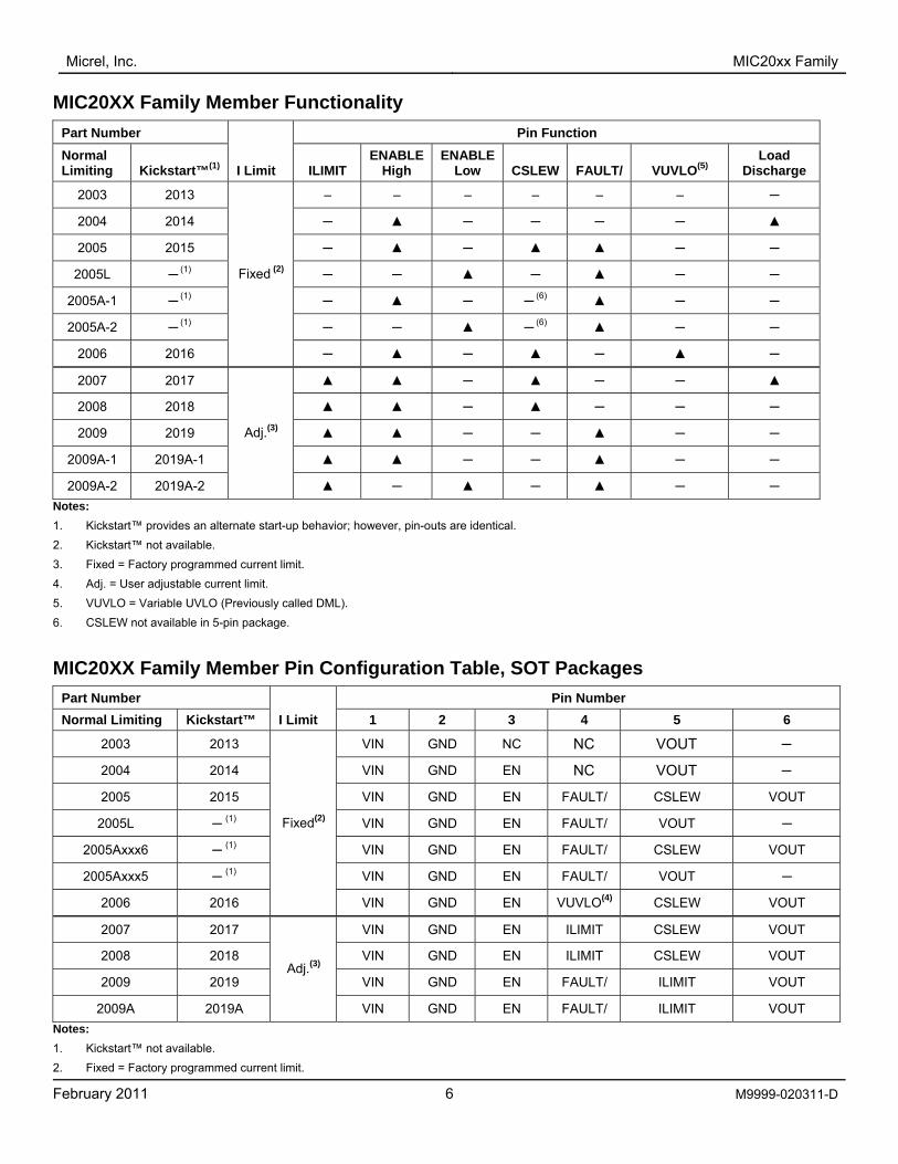
MIC20XX Family Member Functionality Part Number Pin Function Normal Limiting Kickstart™(1) I Limit ILIMIT
ENABLEHigh
ENABLELow CSLEW FAULT/ VUVLO(5)
Load Discharge
2003 2013 – – – – – –
2004 2014
2005 2015
2005L (1)
2005A-1 (1) (6)
2005A-2 (1) (6)
2006 2016
Fixed (2)
2007 2017
2008 2018
2009 2019
2009A-1 2019A-1
2009A-2 2019A-2
Adj.(3)
Notes: 1. Kickstart™ provides an alternate start-up behavior; however, pin-outs are identical. 2. Kickstart™ not available. 3. Fixed = Factory programmed current limit. 4. Adj. = User adjustable current limit. 5. VUVLO = Variable UVLO (Previously called DML). 6. CSLEW not available in 5-pin package.
MIC20XX Family Member Pin Configuration Table, SOT Packages Part Number Pin Number Normal Limiting Kickstart™ I Limit 1 2 3 4 5 6
2003 2013 VIN GND NC NC VOUT
2004 2014 VIN GND EN NC VOUT
2005 2015 VIN GND EN FAULT/ CSLEW VOUT
2005L (1) VIN GND EN FAULT/ VOUT
2005Axxx6 (1) VIN GND EN FAULT/ CSLEW VOUT
2005Axxx5 (1) VIN GND EN FAULT/ VOUT
2006 2016
Fixed(2)
VIN GND EN VUVLO(4) CSLEW VOUT
2007 2017 VIN GND EN ILIMIT CSLEW VOUT
2008 2018 VIN GND EN ILIMIT CSLEW VOUT
2009 2019 VIN GND EN FAULT/ ILIMIT VOUT
2009A 2019A
Adj.(3)
VIN GND EN FAULT/ ILIMIT VOUT Notes: 1. Kickstart™ not available. 2. Fixed = Factory programmed current limit.

Micrel, Inc. MIC20xx Family
February 2011
7 M9999-020311-D
3. ILIMIT = User adjustable current limit. 4. VUVLO = Variable UVLO (Previously called DLM).
MIC20XX Family Member Pin Configuration Table, MLF Packages (5) Part Number Pin Number Normal Limiting Kickstart™ I Limit 6 5 4 3 2 1
2003 2013 VIN GND NC NC NC VOUT
2004 2014 VIN GND EN NC NC VOUT
2005 2015 VIN GND EN FAULT/ CSLEW VOUT
2006 2016
Fixed(2)
VIN GND EN VUVLO(4) CSLEW VOUT
2007 2017 VIN GND EN ILIMIT CSLEW VOUT
2008 2018 VIN GND EN ILIMIT CSLEW VOUT
2009 2019
Adj.(3)
VIN GND EN FAULT/ ILIMIT VOUT Notes: 1. Kickstart™ not available. 2. Fixed = Factory programmed current limit. 3. ILIMIT = User adjustable current limit. 4. VUVLO = Variable UVLO (Previously called DLM). 5. Connect EP to GND.

Micrel, Inc. MIC20xx Family
February 2011
8 M9999-020311-D
MIC20XX Family Member Pin Configuration Drawings
Fixed Current Limit
MIC20X3
VIN
3
1 5
2
4
GND
NC
VOUT
NC
5-Pin SOT-23 (M5) 6-Pin MLF® (ML) (Top View)
MIC20X4
VIN
3
1 5
2
4
GND
ENABLE
VOUT
NC
5-Pin SOT-23 (M5) 6-Pin MLF® (ML) (Top View)
MIC20X5
VIN
3
1 5
2
4
GND
ENABLE
VOUT
FAULT/
VIN
3
1
52GND
ENABLE
VOUT
FAULT/
6
4
CSLEW
5-Pin SOT-23 (M5) MIC2005-X.XL
6-Pin SOT-23 (M6) MIC20X5
6-Pin MLF® (ML) (Top View) MIC20X5
MIC20X6
VIN
3
1
52GND
ENABLE
VOUT
VUVLO
6
4
CSLEW
6-Pin SOT-23 (M6) 6-Pin MLF® (ML) (Top View)

Micrel, Inc. MIC20xx Family
February 2011
9 M9999-020311-D
MIC20XX Family Member Pin Configuration Drawings (continued)
Adjustable Current Limit
MIC20X7/20X8
VIN
3
1
52GND
ENABLE
VOUT
ILIMIT
6
4
CSLEW
6-Pin SOT-23 (M6) 6-Pin MLF® (ML) (Top View)
MIC20X9
VIN
3
1
52GND
ENABLE
VOUT
FAULT/
6
4
ILIMIT
6-Pin SOT-23 (M6) 6-Pin MLF® (ML) (Top View)
MIC2005A
VIN
3
1 5
2
4
GND
ENABLE
VOUT
FAULT/
VIN
3
1
52GND
ENABLE
VOUT
FAULT/
6
4
CSLEW
5-Pin SOT-23 (M5) 6-Pin SOT-23 (M6)
MIC2009A
VIN
3
1
52GND
ENABLE
VOUT
FAULT/
6
4
ILIMIT
6-Pin SOT-23 (M6)
Micrel, Inc. MIC20xx Family
February 2011
10 M9999-020311-D
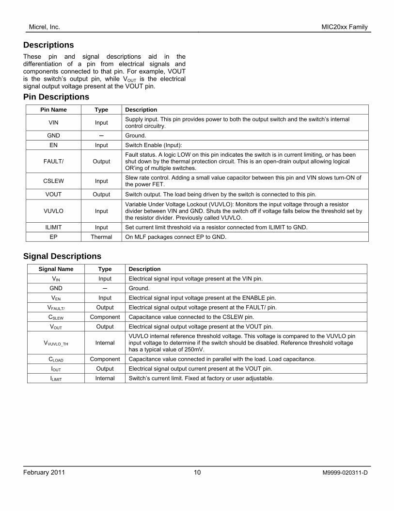
Descriptions These pin and signal descriptions aid in the differentiation of a pin from electrical signals and components connected to that pin. For example, VOUT is the switch’s output pin, while VOUT is the electrical signal output voltage present at the VOUT pin.
Pin Descriptions Pin Name Type Description
VIN Input Supply input. This pin provides power to both the output switch and the switch’s internal control circuitry.
GND Ground. EN Input Switch Enable (Input):
FAULT/ Output Fault status. A logic LOW on this pin indicates the switch is in current limiting, or has been shut down by the thermal protection circuit. This is an open-drain output allowing logical OR’ing of multiple switches.
CSLEW Input Slew rate control. Adding a small value capacitor between this pin and VIN slows turn-ON of the power FET.
VOUT Output Switch output. The load being driven by the switch is connected to this pin.
VUVLO Input Variable Under Voltage Lockout (VUVLO): Monitors the input voltage through a resistor divider between VIN and GND. Shuts the switch off if voltage falls below the threshold set by the resistor divider. Previously called VUVLO.
ILIMIT Input Set current limit threshold via a resistor connected from ILIMIT to GND. EP Thermal On MLF packages connect EP to GND.
Signal Descriptions Signal Name Type Description
VIN Input Electrical signal input voltage present at the VIN pin. GND Ground. VEN Input Electrical signal input voltage present at the ENABLE pin.
VFAULT/ Output Electrical signal output voltage present at the FAULT/ pin. CSLEW Component Capacitance value connected to the CSLEW pin. VOUT Output Electrical signal output voltage present at the VOUT pin.
VVUVLO_TH Internal VUVLO internal reference threshold voltage. This voltage is compared to the VUVLO pin input voltage to determine if the switch should be disabled. Reference threshold voltage has a typical value of 250mV.
CLOAD Component Capacitance value connected in parallel with the load. Load capacitance. IOUT Output Electrical signal output current present at the VOUT pin. ILIMIT Internal Switch’s current limit. Fixed at factory or user adjustable.

Micrel, Inc. MIC20xx Family
February 2011
11 M9999-020311-D
Absolute Maximum Ratings(1) VIN, VOUT ......................................................–0.3V to 6V All other pins.............................................–0.3V to 5.5V Power Dissipation (PD) ....................... Internally Limited Continuous Output Current All except MIC2005A / MIC20X9A................. 2.25A MIC2005A / 20X9A.......................................... 1.0A Maximum Junction Temperature (TJ).................. 150°C Storage Temperature (Ts) .................. –65°C to +150°C Lead Temperature (Soldering 10 sec) ................ 260°C
Operating Ratings(2) Supply Voltage.............................................. 2.5V to 5.5V Continuous Output Current All except MIC2005A / MIC20X9A ........... 0A to 2.1A MIC2005A/20X9A...................................... 0A to 0.9A Ambient Temperature Range (TA) ............–40°C to+85°C Package Thermal Resistance(3) SOT-23-5/6 (θJA) ..........................................230ºC/W 2mm × 2mm MLF® (θJA) .................................90ºC/W 2mm × 2mm MLF® (θJC) .................................45ºC/W
Electrical Characteristics(4) VIN = 5V, TA = 25°C unless otherwise specified. Bold indicates –40°C to +85°C limits; CIN = 1µF.
Symbol Parameter Condition Min Typ Max Units
VIN Switch Input Voltage 2.5 5.5 V
ILEAK Output Leakage Current(5) Switch = OFF, VOUT = 0V Active Low Enable, VEN = 1.5V Active High Enable, VEN = 0V
12 100 µA
MIC2005A, MIC2009A, MIC2019A
Switch = ON Active Low Enable, VEN = 0V Active High Enable, VEN = 1.5V
80 300 µA
Switch = OFF Active Low Enable, VEN = 1.5V 8 15 µA IIN Supply Current(5)
Switch = OFF Active High Enable, VEN = 0V 1 5 µA
170 220 mΩ RDS(ON) Power Switch Resistance VIN = 5V, IOUT = 100mA
275 mΩ
MIC2005A
ILIMIT Fixed Current Limit VOUT = 0.8 × VIN 0.5 0.7 0.9 A
MIC2009A, MIC2019A
IOUT = 0.9A, VOUT = 0.8 × VIN 172 211 263
IOUT = 0.5A, VOUT = 0.8 × VIN 152 206 263
IOUT = 0.2A, VOUT = 0.8 × VIN 138 200 263 CLF Variable Current Limit Factors
IOUT = 0.1A, VOUT = 0.8 × VIN 121 192 263
V
MIC2019A
ILIMIT_2nd Secondary Current Limit VIN = 2.5V, VOUT = 0V 1 2 3 A
Micrel, Inc. MIC20xx Family
February 2011
12 M9999-020311-D
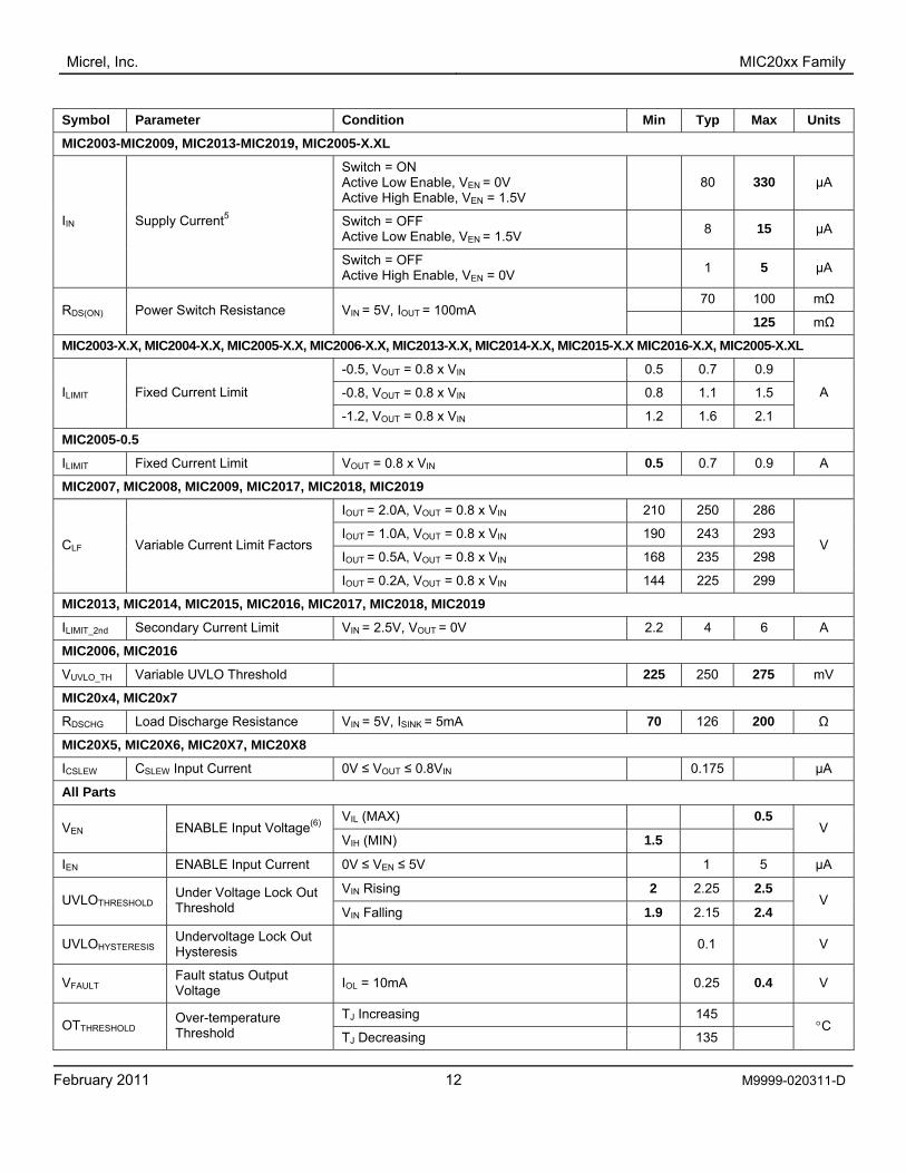
Symbol Parameter Condition Min Typ Max Units
MIC2003-MIC2009, MIC2013-MIC2019, MIC2005-X.XL
Switch = ON Active Low Enable, VEN = 0V Active High Enable, VEN = 1.5V
80 330 µA
Switch = OFF Active Low Enable, VEN = 1.5V 8 15 µA IIN Supply Current5
Switch = OFF Active High Enable, VEN = 0V 1 5 µA
70 100 mΩ RDS(ON) Power Switch Resistance VIN = 5V, IOUT = 100mA
125 mΩ
MIC2003-X.X, MIC2004-X.X, MIC2005-X.X, MIC2006-X.X, MIC2013-X.X, MIC2014-X.X, MIC2015-X.X MIC2016-X.X, MIC2005-X.XL
-0.5, VOUT = 0.8 x VIN 0.5 0.7 0.9
-0.8, VOUT = 0.8 x VIN 0.8 1.1 1.5 ILIMIT Fixed Current Limit
-1.2, VOUT = 0.8 x VIN 1.2 1.6 2.1
A
MIC2005-0.5
ILIMIT Fixed Current Limit VOUT = 0.8 x VIN 0.5 0.7 0.9 A
MIC2007, MIC2008, MIC2009, MIC2017, MIC2018, MIC2019
IOUT = 2.0A, VOUT = 0.8 x VIN 210 250 286
IOUT = 1.0A, VOUT = 0.8 x VIN 190 243 293
IOUT = 0.5A, VOUT = 0.8 x VIN 168 235 298 CLF Variable Current Limit Factors
IOUT = 0.2A, VOUT = 0.8 x VIN 144 225 299
V
MIC2013, MIC2014, MIC2015, MIC2016, MIC2017, MIC2018, MIC2019
ILIMIT_2nd Secondary Current Limit VIN = 2.5V, VOUT = 0V 2.2 4 6 A
MIC2006, MIC2016
VUVLO_TH Variable UVLO Threshold 225 250 275 mV
MIC20x4, MIC20x7
RDSCHG Load Discharge Resistance VIN = 5V, ISINK = 5mA 70 126 200 Ω
MIC20X5, MIC20X6, MIC20X7, MIC20X8
ICSLEW CSLEW Input Current 0V ≤ VOUT ≤ 0.8VIN 0.175 µA
All Parts
VIL (MAX) 0.5 VEN ENABLE Input Voltage(6)
VIH (MIN) 1.5 V
IEN ENABLE Input Current 0V ≤ VEN ≤ 5V 1 5 µA
VIN Rising 2 2.25 2.5 UVLOTHRESHOLD Under Voltage Lock Out
Threshold VIN Falling 1.9 2.15 2.4 V
UVLOHYSTERESIS Undervoltage Lock Out Hysteresis 0.1 V
VFAULT Fault status Output Voltage IOL = 10mA 0.25 0.4 V
TJ Increasing 145 OTTHRESHOLD Over-temperature
Threshold TJ Decreasing 135 °C

Micrel, Inc. MIC20xx Family
February 2011
13 M9999-020311-D
AC Electrical Characteristics Symbol Parameter Condition Min Typ Max Units
tRISE Output Turn-on rise time RL = 10Ω, CLOAD = 1µF, VOUT = 10% to 90% CSLEW
(7) = Open 500 1000 1500 µs
Delay before asserting or releasing FAULT/
MIC2003 – MIC2009 MIC2009A, MIC2005A
Time from current limiting to FAULT/ state change 20 32 49
tD_FAULT Delay before asserting or releasing FAULT/
MIC2013 – MIC2019 MIC2019A
Time from IOUT continuously exceeding primary current limit condition to FAULT/ state change 77 128 192
ms
tD_LIMIT Delay before current limiting
MIC2013 – MIC2019 MIC2019A
77 128 192 ms
tRESET
Delay before resetting Kickstart™ current limit delay, tD_LIMIT
MIC2013 – MIC2019 MIC2019A
Out of current limit following a current limit event. 77 128 192 ms
tON_DLY Output Turn-on Delay RL = 43Ω, CL = 120µF, VEN = 50% to VOUT = 10% *CSLEW = Open
1000 1500 µs
tOFF_DLY Output Turn-off Delay RL = 43Ω, CL = 120µF, VEN = 50% to VOUT = 90% *CSLEW = Open
700 µs
ESD(8)
Symbol Parameter Condition Min Typ Max Units
VOUT and GND ±4 VESD_HB Electro Static Discharge
Voltage: Human Body Model All other pins ±2 kV
VESD_MCHN Electro Static Discharge Voltage; Machine Model
All pins
Machine Model ±200 V
Notes: 1. Exceeding the absolute maximum rating may damage the device. 2. The device is not guaranteed to function outside its operating rating. 3. Requires proper thermal mounting to achieve this performance 4. Specifications for packaged product only. 5. Check the Ordering Information section to determine which parts are Active High or Active Low. 6. VIL(MAX) = Maximum positive voltage applied to the input which will be accepted by the device as a logic low. VIH(MAX) = Maximum positive voltage applied to the input which will be accepted by the device as a logic high. 7. Whenever CSLEW is present. 8. Devices are ESD sensitive. Handling precautions recommended. Human body model, 1.5k in series with 100pF.

Micrel, Inc. MIC20xx Family
February 2011
14 M9999-020311-D
Timing Diagrams
90%
10%
90%
10%
tFALLtRISE
Rise and Fall Times
ENABLE
VOUT
50%
90%
10%
tON_DLY tOFF_DLY
50%
Switching Delay Times

Micrel, Inc. MIC20xx Family
February 2011
15 M9999-020311-D
Typical Characteristics
0
20
40
60
80
100
2.5 3.0 3.5 4.0 4.5 5.0 5.5
SUPP
LY C
UR
REN
T (µ
A)
VIN (V)
Supply Current Output EnabledMIC20XX
-40°C
85°C
25°C
00.010.020.030.040.050.060.070.080.090.10
2.5 3.0 3.5 4.0 4.5 5.0 5.5
SUPP
LY C
UR
REN
T (µ
A)
VIN (V)
Supply Current OutputDisabled (MIC20XX)
-40°C85°C
25°C
00.010.020.030.040.050.060.070.080.090.10
-40 -15 10 35 60 85
LEAK
AGE
CU
RR
ENT
(µA)
TEMPERATURE (°C)
Switch Leakage Current(MIC20XX)
5V
00.10.20.30.40.50.60.70.80.91.0
-40 -15 10 35 60 85
I LIM
IT (A
)
TEMPERATURE (°C)
ILIMIT vs. Temperature(MIC20XX - 0.5)
5V
0.50.60.70.80.91.01.11.21.31.41.5
-40 -15 10 35 60 85
I LIM
IT (A
)
TEMPERATURE (°C)
ILIMIT vs. Temperature(MIC20XX - 0.8)
5V
1.001.101.201.301.401.501.601.701.801.902.00
-40 -15 10 35 60 85
I LIM
IT (A
)
TEMPERATURE (°C)
ILIMIT
vs. Temperature(MIC20XX - 1.2)
5V
020406080
100120140160180200
2 2.5 3 3.5 4 4.5 5 5.5
RD
S(O
N) (
mO
hm)
VIN (V)
RDS(ON) vs. VIN
(MIC20XX)
-40°C
25°C 85°C
020406080
100120140160180200
-40 -15 10 35 60 85
RD
S(O
N) (
mO
hm)
TEMPERATURE (°C)
RDS(ON) vs. Temperature(MIC20XX)
2.5V 3.3V
5.0V
0
200
400
600
800
1000
1200
-40 -15 10 35 60 85CU
RR
ENT-
LIM
IT T
HR
ESH
OLD
(mA)
TEMPERATURE (°C)
ILIMIT vs. Temperature(MIC20X9 - 0.9A)
RSET = 267Ohms
0
20
40
60
80
100
120
140
160
0 0.2 0.4 0.6 0.8 1 1.2
V IN
– V
OU
T (m
V)
IOUT (A)
VDROP vs. Temperature(MIC20XX-1.2)
-40°C
25°C85°C
VIN
= 5.0V
0
20
40
60
80
100
120
140
160
0 0.2 0.4 0.6 0.8 1 1.2
V IN
– V
OU
T (m
V)
IOUT (A)
VDROP vs. Temperature(MIC20XX-1.2)
-40°C
25°C
85°C
VIN
= 3.3V
0
200
400
600
800
1000
1200
0 0.2 0.4 0.6 0.8 1 1.2 1.4
RS
ET
(Ohm
s)
ILIMIT (A)
RSET vs. ILIMIT(MIC20X9)
RSET
=242.62
ILIMIT
0.9538

Micrel, Inc. MIC20xx Family
February 2011
16 M9999-020311-D
Typical Characteristics (cont)
0102030405060708090
100
2.5 3 3.5 4 4.5 5 5.5
SUPP
LY C
UR
RE
NT
(µA)
VIN (V)
Supply Current Output Enabled(MIC20XXA)
-40°C
25°C 85°C
00.010.020.030.040.050.060.070.080.090.10
2.5 3 3.5 4 4.5 5 5.5
SUPP
LY C
UR
RE
NT
(µA)
VIN (V)
Supply Current OutputDisabled (MIC20XXA)
-40°C 25°C85°C
00.010.020.030.040.050.060.070.080.090.10
-40 -15 10 35 60 85
LEAK
AGE
CU
RR
ENT
(µA)
TEMPERATURE (°C)
Switch Leakage Current(MIC20XXA)
5V
00.10.20.30.40.50.60.70.80.91.0
-40 -15 10 35 60 85
I LIM
IT (A
)
TEMPERATURE (°C)
ILIMIT vs. Temperature(MIC20X5A)
5V
0100200300400500600700800900
1000
-40 -15 10 35 60 85
I LIM
IT (A
)
TEMPERATURE (°C)
ILIMIT vs. Temperature(MIC20X9A (0.8A))
RSET
= 267Ohms
0
500
1000
1500
2000
2500
0 0.2 0.4 0.6 0.8 1
RS
ET
(Ohm
s)
ILIMIT (A)
RSET vs. ILIMIT(MIC20X9A)
RSET
=212.23
ILIMIT
0.9587
0
50
100
150
200
250
2.5 3 3.5 4 4.5 5 5.5
RD
S(O
N) (
mO
hms)
VIN (V)
RDS(ON) vs. VIN(MIC20XXA)
-40°C
25°C 85°C
0
50
100
150
200
250
-40 -15 10 35 60 85
RD
S(O
N) (
mO
hms)
TEMPERATURE (°C)
RDS(ON) vs. Temperature(MIC20XXA)
5.0V
2.5V 3.3V
0
5
10
15
20
25
30
35
40
-40 -15 10 35 60 85
FLAG
DE
LAY
(ms)
TEMPERATURE (°C)
Flag Delayvs. Temperature
2.5V3.3V
5.0V
0
20
40
60
80
100
120
140
160
0 0.1 0.2 0.3 0.4 0.5 0.6
V IN
- V O
UT
(mV)
IOUT (A)
VDROP vs. Temperature(MIC20XXA)
-40°C
25°C85°C
VIN
= 5.0V
0
20
40
60
80
100
120
140
160
0 0.1 0.2 0.3 0.4 0.5 0.6
V IN
- V O
UT
(mV)
IOUT (A)
VDROP vs. Temperature(MIC20XXA)
-40°C
25°C85°C
VIN
= 3.3V
2.05
2.1
2.15
2.2
2.25
2.3
-50 0 50 100 150
THR
ESH
OLD
(V)
TEMPERATURE (°C)
UVLO Thresholdvs. Temperature
V RISING
V FALLING
Micrel, Inc. MIC20xx Family
February 2011
17 M9999-020311-D
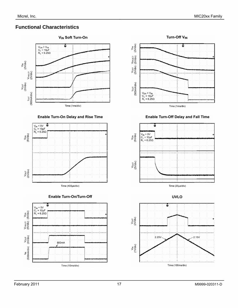
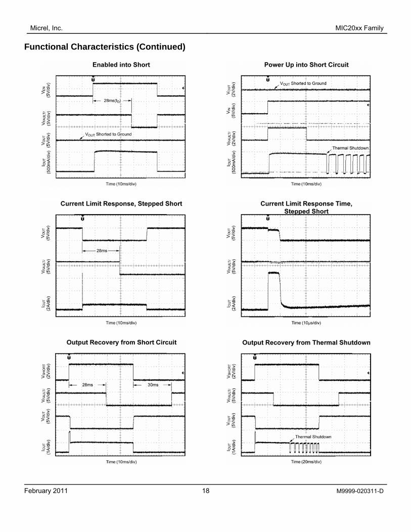
Functional Characteristics
Micrel, Inc. MIC20xx Family
February 2011
18 M9999-020311-D
Functional Characteristics (Continued)

Micrel, Inc. MIC20xx Family
February 2011
19 M9999-020311-D
Functional Characteristics (Continued)

Micrel, Inc. MIC20xx Family
February 2011
20 M9999-020311-D
Functional Diagram
Figure 2 MIC20XX Family Functional Diagram

Micrel, Inc. MIC20xx Family
February 2011
21 M9999-020311-D
Functional Description
VIN and VOUT VIN is both the power supply connection for the internal circuitry driving the switch and the input (Source connection) of the power MOSFET switch. VOUT is the Drain connection of the power MOSFET and supplies power to the load. In a typical circuit, current flows from VIN to VOUT toward the load. Since the switch is bi-directional when enabled, if VOUT is greater than VIN, current will flow from VOUT to VIN. When the switch is disabled, current will not flow to the load, except for a small unavoidable leakage current of a few microamps. However, should VOUT exceed VIN by more than a diode drop (~0.6 V), while the switch is disabled, current will flow from output to input via the power MOSFET’s body diode. If discharging CLOAD is required by your application, consider using MIC20X4 or MIC20X7; these MIC20XX family members are equipped with a discharge FET to insure complete discharge of CLOAD.
Current Sensing and Limiting MIC20XX protects the system power supply and load from damage by continuously monitoring current through the on-chip power MOSFET. Load current is monitored by means of a current mirror in parallel with the power MOSFET switch. Current limiting is invoked when the load exceeds the set over-current threshold. When current limiting is activated the output current is constrained to the limit value, and remains at this level until either the load/fault is removed, the load’s current requirement drops below the limiting value, or the switch goes into thermal shutdown.
Kickstart™ 2003 2004 2005X 2006 2007 2008 2009X
2013 2014 2015 2016 2017 2018 2019X
Only parts in bold have Kickstart™. (Not available in 5-pin SOT-23 packages)
The MIC201X is designed to allow momentary current surges (Kickstart™) before the onset of current limiting, which permits dynamic loads, such as small disk drives or portable printers to draw the energy needed to overcome inertial loads without sacrificing system safety. In this respect, the Kickstart™ parts (MIC201X) differs markedly from the non-Kickstart™ parts (MIC200X) which immediately limit load current, potentially starving the motor and causing the appliance to stall or stutter. During this delay period, typically 128ms, a secondary current limit is in effect. If the load demands a current in excess the secondary limit, MIC201X acts immediately to restrict output current to the secondary limit for the duration of the Kickstart™ period. After this time the MIC201X reverts to its normal current limit. An example
of Kickstart™ operation is shown below.
Figure 3. Kickstart™ Operation
Figure 3 Label Key: A. MIC201X is enabled into an excessive load
(slew rate limiting not visible at this time scale) The initial current surge is limited by either the overall circuit resistance and power supply compliance, or the secondary current limit, whichever is less.
B. RON of the power FET increases due to internal heating (effect exaggerated for emphasis).
C. Kickstart™ period. D. Current limiting initiated. FAULT/ goes LOW. E. VOUT is non-zero (load is heavy, but not a dead
short where VOUT = 0V. Limiting response will be the same for dead shorts).
F. Thermal shutdown followed by thermal cycling. G. Excessive load released, normal load remains.
MIC201X drops out of current limiting. H. FAULT/ delay period followed by FAULT/ going
HIGH.
Under Voltage Lock Out Under voltage lock-out insures no anomalous operation occurs before the device’s minimum input voltage of UVLOTHRESHOLD which is 2V minimum, 2.25V typical, and 2.5V maximum had been achieved. Prior to reaching this voltage, the output switch (power MOSFET) is OFF and no circuit functions, such as FAULT/ or ENABLE, are considered to be valid or operative.

Micrel, Inc. MIC20xx Family
February 2011
22 M9999-020311-D
Variable Under Voltage Lock Out (VUVLO) 2003 2004 2005X 2006 2007 2008 2009X
2013 2014 2015 2016 2017 2018 2019X Only parts in bold have VUVLO.
VUVLO functions as an input voltage monitor when the switch in enabled. The VIN pin is monitored for a drop in voltage, indicating excessive loading of the VIN supply. When VIN is less than the VULVO threshold voltage (VVUVLO_TH) for 32ms or more, the MIC20XX disables the switch to protect the supply and allow VIN to recover. After 128ms has elapsed, the MIC20X6 enables switch. This disable and enable cycling will continue as long as VIN deceases below the VUVLO threshold voltage (VVUVLO_TH) which has a typical value of 250mV. The VUVLO voltage is commonly established by a voltage divider from VIN-to-GND.
ENABLE 2003 2004 2005X 2006 2007 2008 2009X
2013 2014 2015 2016 2017 2018 2019X Only parts in bold have ENABLE pin.
ENABLE pin is a logic compatible input which activates the main MOSFET switch thereby providing power to the VOUT pin. ENABLE is either an active HIGH or active LOW control signal. The MIC20XX can operate with logic running from supply voltages as low as 1.5 V. ENABLE may be driven higher than VIN, but no higher than 5.5V and not less than –0.3V.
FAULT/ 2003 2004 2005X 2006 2007 2008 2009X
2013 2014 2015 2016 2017 2018 2019X Only parts in bold have FAULT/ pin.
FAULT/ is an N-channel open-drain output, which is asserted (LOW true) when switch either begins current limiting or enters thermal shutdown. FAULT/ asserts after a brief delay when events occur that may be considered possible faults. This delay insures that FAULT/ is asserted only upon valid, enduring, over-current conditions and that transitory event error reports are filtered out. In MIC200X FAULT/ asserts after a brief delay period, of 32ms typical. After a fault clears, FAULT/ remains asserted for the delay period of 32ms MIC201X’s FAULT/ asserts at the end of the Kickstart™ period which is 128ms typical. This masks initial current surges, such as would be seen by a motor load starting up. If the load current remains above the current limit threshold after the Kickstart™ has timed out, then the FAULT/ will be asserted. After a fault clears, FAULT/ remains asserted for the delay of 128ms. Because FAULT/ is an open-drain it must be pulled HIGH with an external resistor and it may be wire-OR’d
with other similar outputs, sharing a single pull-up resistor. FAULT/ may be tied to a pull-up voltage source which is higher than VIN, but no greater than 5.5V.
Soft-start Control Large capacitive loads can create significant inrush current surges when charged through the switch. For this reason, the MIC20XX family of switches provides a built-in soft-start control to limit the initial inrush currents. Soft-start is accomplished by controlling the power MOSFET when the ENABLE pin enables the switch.
CSLEW 2003 2004 2005X 2006 2007 2008 2009X
2013 2014 2015 2016 2017 2018 2019X Only parts in bold have CSLEW pin. (Not available in 5-pin SOT-23 packages)
The CSLEW pin is provided to increase control of the output voltage ramp at turn-on. This input allows designers the option of decreasing the output’s slew rate (slowing the voltage rise) by adding an external capacitance between the CSLEW and VIN pins.
Thermal Shutdown Thermal shutdown is employed to protect the MIC20XX family of switches from damage should the die temperature exceed safe operating levels. Thermal shutdown shuts off the output MOSFET and asserts the FAULT/ output if the die temperature reaches 145°C. The switch will automatically resume operation when the die temperature cools down to 135°C. If resumed operation results in reheating of the die, another shutdown cycle will occur and the switch will continue cycling between ON and OFF states until the overcurrent condition has been resolved. Depending on PCB layout, package type, ambient temperature, etc., hundreds of milliseconds may elapse from the incidence of a fault to the output MOSFET being shut off. This delay is due to thermal time constants within the system itself. In no event will the device be damaged due to thermal overload because die temperature is monitored continuously by on-chip circuitry.
Micrel, Inc. MIC20xx Family
February 2011
23 M9999-020311-D
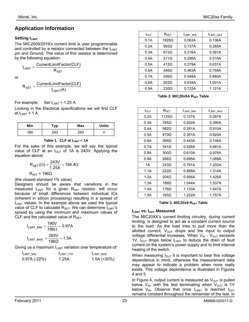
Application Information
Setting ILIMIT The MIC2009/2019’s current limit is user programmable and controlled by a resistor connected between the ILIMIT pin and Ground. The value of this resistor is determined by the following equation:
SETLIMIT R
LF)itFactor(CCurrentLimI =
or
(A)ILF)itFactor(CCurrentLimR
LIMITSET =
For example: Set ILIMIT = 1.25 A Looking in the Electrical specifications we will find CLF at ILIMIT = 1 A.
Min Typ Max Units
190 243 293 V
Table 1. CLF at ILIMIT = 1A For the sake of this example, we will say the typical value of CLF at an IOUT of 1A is 243V. Applying the equation above:
Ω==Ω 4.1941.25A243V)(RSET
RSET = 196Ω (the closest standard 1% value) Designers should be aware that variations in the measured ILIMIT for a given RSET resistor, will occur because of small differences between individual ICs (inherent in silicon processing) resulting in a spread of ILIMIT values. In the example above we used the typical value of CLF to calculate RSET. We can determine ILIMIT’s spread by using the minimum and maximum values of CLF and the calculated value of RSET.
A97.0196190VILIMIT_MIN =
Ω=
1.5A196Ω293VILIMIT_MAX ==
Giving us a maximum ILIMIT variation over temperature of: ILIMIT_MIN ILIMIT_TYP ILIMIT_MAX 0.97A (-22%) 1.25A 1.5A (+20%)
IOUT RSET ILIMIT_MIN ILIMIT_MAX 0.1A 1928Ω 0.063A 0.136A 0.2A 993Ω 0.137A 0.265A 0.3A 673Ω 0.216A 0.391A 0.4A 511Ω 0.296A 0.515A 0.5A 413Ω 0.379A 0.637A 0.6A 346Ω 0.463A 0.759A 0.7A 299Ω 0.548A 0.880A 0.8A 263Ω 0.634A 1.001A 0.9A 235Ω 0.722A 1.121A
Table 2. MIC20x9A RSET Table
IOUT RSET ILIMIT_MIN ILIMIT_MAX 0.2A 1125Ω 0.127A 0.267A 0.3A 765Ω 0.202A 0.390A 0.4A 582Ω 0.281A 0.510A 0.5A 470Ω 0.361A 0.629A 0.6A 395Ω 0.443A 0.746A 0.7A 341Ω 0.526A 0.861A 0.8A 300Ω 0.610A 0.976A 0.9A 268Ω 0.695A 1.089A 1A 243Ω 0.781A 1.202A
1.1A 222Ω 0.868A 1.314A 1.2A 204Ω 0.956A 1.426A 1.3A 189Ω 1.044A 1.537A 1.4A 176Ω 1.133A 1.647A 1.5A 165Ω 1.222A 1.757A
Table 3. MIC20x9 RSET Table
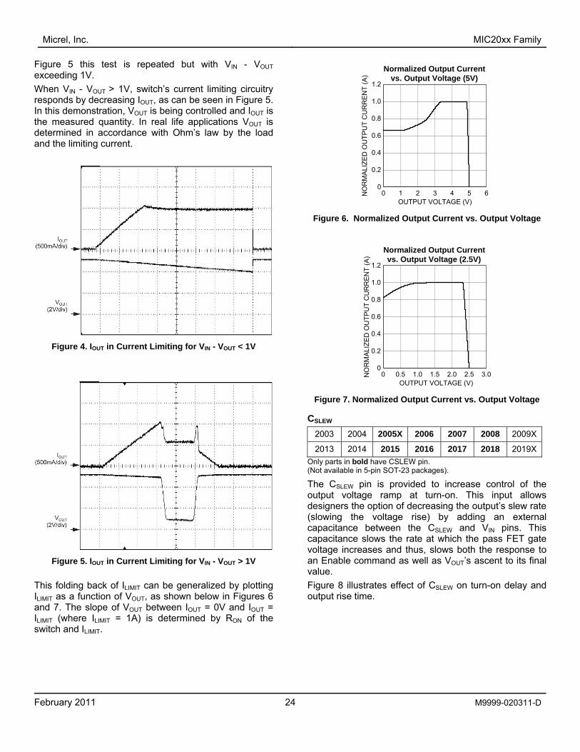
ILIMIT vs. IOUT Measured The MIC20XX’s current limiting circuitry, during current limiting, is designed to act as a constant current source to the load. As the load tries to pull more than the allotted current, VOUT drops and the input to output voltage differential increases. When VIN - VOUT exceeds 1V, IOUT drops below ILIMIT to reduce the drain of fault current on the system’s power supply and to limit internal heating of the switch. When measuring IOUT it is important to bear this voltage dependence in mind, otherwise the measurement data may appear to indicate a problem when none really exists. This voltage dependence is illustrated in Figures 4 and 5. In Figure 4, output current is measured as VOUT is pulled below VIN, with the test terminating when VOUT is 1V below VIN. Observe that once ILIMIT is reached IOUT remains constant throughout the remainder of the test. In
Micrel, Inc. MIC20xx Family
February 2011
24 M9999-020311-D
Figure 5 this test is repeated but with VIN - VOUT exceeding 1V. When VIN - VOUT > 1V, switch’s current limiting circuitry responds by decreasing IOUT, as can be seen in Figure 5. In this demonstration, VOUT is being controlled and IOUT is the measured quantity. In real life applications VOUT is determined in accordance with Ohm’s law by the load and the limiting current.
Figure 4. IOUT in Current Limiting for VIN - VOUT < 1V
Figure 5. IOUT in Current Limiting for VIN - VOUT > 1V This folding back of ILIMIT can be generalized by plotting ILIMIT as a function of VOUT, as shown below in Figures 6 and 7. The slope of VOUT between IOUT = 0V and IOUT = ILIMIT (where ILIMIT = 1A) is determined by RON of the switch and ILIMIT.
0
0.2
0.4
0.6
0.8
1.0
1.2
0 1 2 3 4 5 6NO
RM
ALI
ZED
OU
TPU
T C
UR
RE
NT
(A)
OUTPUT VOLTAGE (V)
Normalized Output Currentvs. Output Voltage (5V)
Figure 6. Normalized Output Current vs. Output Voltage
0
0.2
0.4
0.6
0.8
1.0
1.2
0 0.5 1.0 1.5 2.0 2.5 3.0NO
RM
ALIZ
ED
OU
TPU
T C
UR
REN
T (A
)
OUTPUT VOLTAGE (V)
Normalized Output Currentvs. Output Voltage (2.5V)
Figure 7. Normalized Output Current vs. Output Voltage
CSLEW 2003 2004 2005X 2006 2007 2008 2009X
2013 2014 2015 2016 2017 2018 2019X Only parts in bold have CSLEW pin. (Not available in 5-pin SOT-23 packages).
The CSLEW pin is provided to increase control of the output voltage ramp at turn-on. This input allows designers the option of decreasing the output’s slew rate (slowing the voltage rise) by adding an external capacitance between the CSLEW and VIN pins. This capacitance slows the rate at which the pass FET gate voltage increases and thus, slows both the response to an Enable command as well as VOUT’s ascent to its final value. Figure 8 illustrates effect of CSLEW on turn-on delay and output rise time.

Micrel, Inc. MIC20xx Family
February 2011
25 M9999-020311-D
0
0.002
0.004
0.006
0.008
0.01
0.012
0.014
0 0 0 0 0 0 0 0 0 0
TIM
E (m
S)
CSLEW (nF)
Typical Turn-on Timesvs. External CSLEW Capacitance
2
4
6
8
10
12
14
00 0.5 1 1.5 2 2.5 3 3.5 4 4.5
TRISE
TDELAY
TON
Figure 8. CSLEW vs. Turn-On, Delay and Rise TImes
CSLEW’s effect on ILIMIT An unavoidable consequence of adding CSLEW capacitance is a reduction in the MIC20X5 – 20X8’s ability to quickly limit current transients or surges. A sufficiently large capacitance can prevent both the primary and secondary current limits from acting in time to prevent damage to the MIC20X5 – 20X8 or the system from a short circuit fault. For this reason, the upper limit on the value of CSLEW is 4nF.
Variable Under Voltage Lock Out (VUVLO) 2003 2004 2005X 2006 2007 2008 2009X
2013 2014 2015 2016 2017 2018 2019X
Only parts in bold have VUVLO pin and functionality.
Power conscious systems, such as those implementing ACPI, will remain active even in their low power states and may require the support of external devices through both phases of operation. Under these conditions, the current allowed these external devices may vary according to the system’s operating state and as such require dual current limits on their peripheral ports. The MIC20X6 is designed for systems demanding two primary current limiting levels but without the use of a control signal to select between current limits. To better understand how the MIC20X6 provides this, imagine a system whose main power supply supports heavy loads during normal operation, but in sleep mode is reduced to only few hundred milliamps of output current. In addition, this system has several USB ports which must remain active during sleep. During normal operation, each port can support a 500mA peripheral, but in sleep mode their combined output current is limited to what the power supply can deliver minus whatever the system itself is drawing. If a peripheral device is plugged in which demands more current than is available, the system power supply will sag, or crash. The MIC20X6 prevents this by monitoring both the load current and VIN. During normal operation, when the power supply can source plenty of current, the MIC20X6 will support any load up to its factory
programmed current limit. When the weaker, standby supply is in operation, the MIC20X6 monitors VIN and will shut off its output should VIN dip below a predetermined value. This predetermined voltage is user programmable and set by the selection of the resistor divider driving the VUVLO pin. To prevent false triggering of the VUVLO feature, the MIC20X6 includes a delay timer to blank out momentary excursions below the VUVLO trip point. If VIN stays below the VUVLO trip point for longer than 32ms (typical), then the load is disengaged and the MIC20X6 will wait 128ms before reapplying power to the load. If VIN remains below the VUVLO trip point, then the load will be powered for the 32ms blanking period and then again disengaged. This is illustrated in the scope plot below. If VIN remains above the VUVLO trip point MIC20X6 resumes normal operation.
Figure 9. VUVLO Operation VUVLO and Kickstart™ operate independently in the MIC2016. If the high current surge allowed by Kickstart™ causes VIN to dip below the VUVLO trip point for more than 32ms, VUVLO will disengage the load even though the Kickstart™ timer has not timed out.
VIN
MIC20X6
VOUT
VUVLO
InputSupply
R1
R2
++
IIN_LOAD
Figure 10. VUVLO Application Circuit
Calculating VUVLO Resistor Divider Values The VUVLO feature is designed to keep the internal switch off until the voltage on the VUVLO pin is greater than 0.25V. A resistor divider network connected to the VUVLO and VIN pins is used to set the input trip voltage VTRIP, see Figure 10. The value of R2 is chosen to minimize the load on the input supply IDIV and the value of R1 sets the trip voltage VTRIP.
Micrel, Inc. MIC20xx Family
February 2011
26 M9999-020311-D
The value of R2 is calculated using:
DIV
VUVLO
IV
2R =
The vale of R1 is calculated using:
⎟⎟⎠
⎞⎜⎜⎝
⎛−×= 1
V
VR2R1
VUVLO
TRIP
Where for both equations: VVUVLO = 0.25V
When working with large value resistors, a small amount of leakage current from the VUVLO terminal can cause voltage offsets that degrade system accuracy. Therefore, the maximum recommended resistor value for R2 is 100kΩ. Using the divider loading current IDIV of 100uA, the value of R2 can be estimated by:
Ω== k5.2µA100V25.02R
Now the value of R1 can be calculated by:
k451V25.0V75.4k5.21R =⎟
⎠⎞
⎜⎝⎛ −×Ω=
Where: VTRIP = 4.75V (for a 5V supply) VVUVLO = 0.25V
The VUVLO comparator uses no Hysteresis. This is because the VUVLO blanking timer prevents any chattering that might otherwise occur if VIN varies about the trigger point. The timer is reset by upward crossings of the trip point such that VIN must remain below the trip point for the full 32ms period for load disengagement to occur. In selecting a VTRIP voltage, the designer is cautioned to not make this value less than 2.5V. A minimum of 2.5V is required for the MIC20X6’s internal circuitry to operate properly. VUVLO trip points below 2.5V will result in erratic or unpredictable operation.
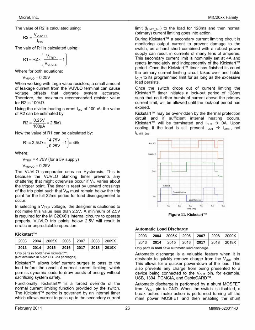
Kickstart™ 2003 2004 2005X 2006 2007 2008 2009X
2013 2014 2015 2016 2017 2018 2019X
Only parts in bold have Kickstart™. (Not available in 5-pin SOT-23 packages).
Kickstart™ allows brief current surges to pass to the load before the onset of normal current limiting, which permits dynamic loads to draw bursts of energy without sacrificing system safety. Functionally, Kickstart™ is a forced override of the normal current limiting function provided by the switch. The Kickstart™ period is governed by an internal timer which allows current to pass up to the secondary current
limit (ILIMIT_2nd) to the load for 128ms and then normal (primary) current limiting goes into action. During Kickstart™ a secondary current limiting circuit is monitoring output current to prevent damage to the switch, as a hard short combined with a robust power supply can result in currents of many tens of amperes. This secondary current limit is nominally set at 4A and reacts immediately and independently of the Kickstart™ period. Once the Kickstart™ timer has finished its count the primary current limiting circuit takes over and holds IOUT to its programmed limit for as long as the excessive load persists. Once the switch drops out of current limiting the Kickstart™ timer initiates a lock-out period of 128ms such that no further bursts of current above the primary current limit, will be allowed until the lock-out period has expired. Kickstart™ may be over-ridden by the thermal protection circuit and if sufficient internal heating occurs, Kickstart™ will be terminated and IOUT 0A. Upon cooling, if the load is still present IOUT ILIMIT, not ILIMIT_2nd.
Figure 11. Kickstart™
Automatic Load Discharge 2003 2004 2005X 2006 2007 2008 2009X
2013 2014 2015 2016 2017 2018 2019X Only parts in bold have automatic load discharge.
Automatic discharge is a valuable feature when it is desirable to quickly remove charge from the VOUT pin. This allows for a quicker power-down of the load. This also prevents any charge from being presented to a device being connected to the VOUT pin, for example, USB, 1394, PCMCIA, and CableCARD™. Automatic discharge is performed by a shunt MOSFET from VOUT pin to GND. When the switch is disabled, a break before make action is performed turning off the main power MOSFET and then enabling the shunt

Micrel, Inc. MIC20xx Family
February 2011
27 M9999-020311-D
MOSFET. The total resistance of the MOSFET and internal resistances is typically 126Ω.
Supply Filtering A minimum 1μF bypass capacitor positioned close to the VIN and GND pins of the switch is both good design practice and required for proper operation of the switch. This will control supply transients and ringing. Without a bypass capacitor, large current surges or a short may cause sufficient ringing on VIN (from supply lead inductance) to cause erratic operation of the switch’s control circuitry. For best performance good quality, low ESR capacitors are recommended, preferably ceramic.
When bypassing with capacitors of 10μF and up, it is good practice to place a smaller value capacitor in parallel with the larger to handle the high frequency components of any line transients. Values in the range of 0.01μF to 0.1μF are recommended. Again, good quality, low ESR capacitors should be chosen.
Power Dissipation Power dissipation depends on several factors such as the load, PCB layout, ambient temperature, and supply voltage. Calculation of power dissipation can be accomplished by the following equation:
2
)I(RP OUT)ON(DSD ×=
To relate this to junction temperature, the following equation can be used:
A)AJ(DJ TRPT +×= −θ
Where: TJ = junction temperature, TA = ambient temperature Rθ(J-A) is the thermal resistance of the package
In normal operation the switch’s RON is low enough that no significant I2R heating occurs. Device heating is most often caused by a short circuit, or very heavy load, when a significant portion of the input supply voltage appears across the switch’s power MOSFET. Under these conditions the heat generated will exceed the package and PCB’s ability to cool the device and thermal limiting will be invoked. In Figure 12 die temperature is plotted against IOUT
assuming a constant case temperature of 85°C. The plots also assume a worst case RON of 140mΩ at a die temperature of 135°C. Under these conditions it is clear that an SOT-23 packaged device will be on the verge of thermal shutdown, typically 140°C die temperature, when operating at a load current of 1.25A. For this reason we recommend using MLF® packaged switches for any design intending to supply continuous currents of 1A or more.
0
20
40
60
80
100
120
140
160
0.2OUTPUT CURRENT (A)
Die Temperature vs.Output Current (T CASE=85°C)
SOT-23
0.4 0.6 0.8 1.0 1.2 1.4 1.6 1.8 2.0
MLF
Figure 12. Die Temperature vs. IOUT

Micrel, Inc. MIC20xx Family
February 2011
28 M9999-020311-D
Package Information
5-Pin SOT-23 (M5)
6-Pin SOT-23 (M6)

Micrel, Inc. MIC20xx Family
6 Pin 2mm x 2mm MLF® (ML)
February 2011 9-020311-D
29 M999
MICREL, INC. 2180 FORTUNE DRIVE SAN JOSE, CA 95131 USA TEL +1 (408) 944-0800 FAX +1 (408) 474-1000 WEB http://www.micrel.com
Micrel makes no representations or warranties with respect to the accuracy or completeness of the information furnished in this data sheet. This
information is not intended as a warranty and Micrel does not assume responsibility for its use. Micrel reserves the right to change circuitry, specifications and descriptions at any time without notice. No license, whether express, implied, arising by estoppel or otherwise, to any intellectual
property rights is granted by this document. Except as provided in Micrel’s terms and conditions of sale for such products, Micrel assumes no liability whatsoever, and Micrel disclaims any express or implied warranty relating to the sale and/or use of Micrel products including liability or warranties
relating to fitness for a particular purpose, merchantability, or infringement of any patent, copyright or other intellectual property right.
Micrel Products are not designed or authorized for use as components in life support appliances, devices or systems where malfunction of a product reasonably be expected to result in personal injury. Life support devices or systems are devices or systems that (a) are intended for surgical implainto the body or (b) support or sustain life, and whose failure to perform can be reasonably expected to result in a significant injury to the user. A
Purchaser’s use or sale of Micrel Products for use in life support appliances, devices or systems is a Purchaser’s own risk and Purchaser agrees to fully indemnify Micrel for any damages resulting from such use or sale.
can nt
© 2009 Micrel, Incorporated.