MIC2213 Micrel, Inc. MIC2213 - Microchip...
11
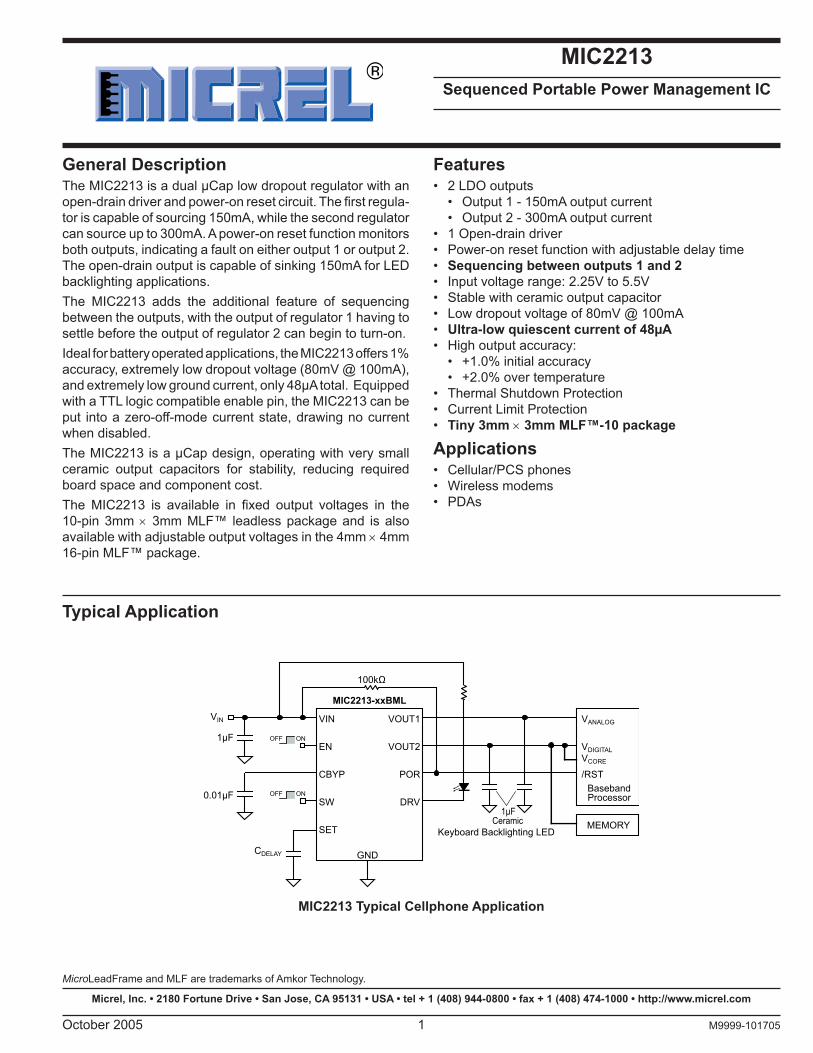
October 2005 1 M9999-101705 MIC2213 Micrel, Inc. MIC2213 Sequenced Portable Power Management IC General Description The MIC2213 is a dual µCap low dropout regulator with an open-drain driver and power-on reset circuit. The first regula- tor is capable of sourcing 150mA, while the second regulator can source up to 300mA. A power-on reset function monitors both outputs, indicating a fault on either output 1 or output 2. The open-drain output is capable of sinking 150mA for LED backlighting applications. The MIC2213 adds the additional feature of sequencing between the outputs, with the output of regulator 1 having to settle before the output of regulator 2 can begin to turn-on. Ideal for battery operated applications, the MIC2213 offers 1% accuracy, extremely low dropout voltage (80mV @ 100mA), and extremely low ground current, only 48µA total. Equipped with a TTL logic compatible enable pin, the MIC2213 can be put into a zero-off-mode current state, drawing no current when disabled. The MIC2213 is a µCap design, operating with very small ceramic output capacitors for stability, reducing required board space and component cost. The MIC2213 is available in fixed output voltages in the 10-pin 3mm × 3mm MLF™ leadless package and is also available with adjustable output voltages in the 4mm × 4mm 16-pin MLF™ package. Typical Application VIN V IN C DELAY EN CBYP SW 0.01µF 1µF 100kΩ SET Keyboard Backlighting LED Baseband VOUT1 V ANALOG VOUT2 POR V DIGITAL V CORE /RST DRV GND MIC2213-xxBML 1µF OFF ON OFF ON MEMORY Ceramic Processor MIC2213 Typical Cellphone Application Features • 2 LDO outputs • Output 1 - 150mA output current • Output 2 - 300mA output current • 1 Open-drain driver • Power-on reset function with adjustable delay time • Sequencing between outputs 1 and 2 • Input voltage range: 2.25V to 5.5V • Stable with ceramic output capacitor • Low dropout voltage of 80mV @ 100mA • Ultra-low quiescent current of 48µA • High output accuracy: • +1.0% initial accuracy • +2.0% over temperature • Thermal Shutdown Protection • Current Limit Protection • Tiny 3mm × 3mm MLF™-10 package Applications • Cellular/PCS phones • Wireless modems • PDAs Micrel, Inc. • 2180 Fortune Drive • San Jose, CA 95131 • USA • tel + 1 (408) 944-0800 • fax + 1 (408) 474-1000 • http://www.micrel.com MicroLeadFrame and MLF are trademarks of Amkor Technology.
Transcript of MIC2213 Micrel, Inc. MIC2213 - Microchip...
October 2005 1 M9999-101705
MIC2213 Micrel, Inc.
MIC2213Sequenced Portable Power Management IC
General DescriptionThe MIC2213 is a dual µCap low dropout regulator with an open-drain driver and power-on reset circuit. The first regula-tor is capable of sourcing 150mA, while the second regulator can source up to 300mA. A power-on reset function monitors both outputs, indicating a fault on either output 1 or output 2. The open-drain output is capable of sinking 150mA for LED backlighting applications.The MIC2213 adds the additional feature of sequencing between the outputs, with the output of regulator 1 having to settle before the output of regulator 2 can begin to turn-on.Ideal for battery operated applications, the MIC2213 offers 1% accuracy, extremely low dropout voltage (80mV @ 100mA), and extremely low ground current, only 48µA total. Equipped with a TTL logic compatible enable pin, the MIC2213 can be put into a zero-off-mode current state, drawing no current when disabled.The MIC2213 is a µCap design, operating with very small ceramic output capacitors for stability, reducing required board space and component cost.The MIC2213 is available in fixed output voltages in the 10-pin 3mm × 3mm MLF™ leadless package and is also available with adjustable output voltages in the 4mm × 4mm 16-pin MLF™ package.
Typical Application
VINVIN
CDELAY
EN
CBYP
SW0.01µF
1µF
100kΩ
SET Keyboard Backlighting LED
Baseband
VOUT1 VANALOG
VOUT2
POR
VDIGITALVCORE
/RST
DRV
GND
MIC2213-xxBML
1µF
OFF ON
OFF ON
MEMORYCeramic
Processor
MIC2213 Typical Cellphone Application
Features• 2 LDO outputs
• Output 1 - 150mA output current • Output 2 - 300mA output current
• 1 Open-drain driver• Power-on reset function with adjustable delay time• Sequencing between outputs 1 and 2• Input voltage range: 2.25V to 5.5V• Stable with ceramic output capacitor• Low dropout voltage of 80mV @ 100mA• Ultra-low quiescent current of 48µA• High output accuracy:
• +1.0% initial accuracy • +2.0% over temperature
• Thermal Shutdown Protection• Current Limit Protection• Tiny 3mm × 3mm MLF™-10 package
Applications• Cellular/PCS phones• Wireless modems• PDAs
Micrel, Inc. • 2180 Fortune Drive • San Jose, CA 95131 • USA • tel + 1 (408) 944-0800 • fax + 1 (408) 474-1000 • http://www.micrel.com
MicroLeadFrame and MLF are trademarks of Amkor Technology.
MIC2213 Micrel, Inc.
M9999-101705 2 October 2005
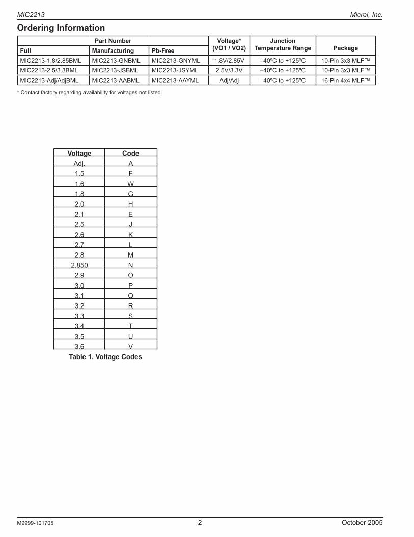
Ordering InformationPart Number Voltage*
(VO1 / VO2)Junction
Temperature Range
PackageFull Manufacturing Pb-FreeMIC2213-1.8/2.85BML MIC2213-GNBML MIC2213-GNYML 1.8V/2.85V –40ºC to +125ºC 10-Pin 3x3 MLF™MIC2213-2.5/3.3BML MIC2213-JSBML MIC2213-JSYML 2.5V/3.3V –40ºC to +125ºC 10-Pin 3x3 MLF™MIC2213-Adj/AdjBML MIC2213-AABML MIC2213-AAYML Adj/Adj –40ºC to +125ºC 16-Pin 4x4 MLF™
* Contact factory regarding availability for voltages not listed.
Voltage Code Adj. A 1.5 F 1.6 W 1.8 G 2.0 H 2.1 E 2.5 J 2.6 K 2.7 L 2.8 M 2.850 N 2.9 O 3.0 P 3.1 Q 3.2 R 3.3 S 3.4 T 3.5 U 3.6 V
Table 1. Voltage Codes
October 2005 3 M9999-101705
MIC2213 Micrel, Inc.
1
2
3
4
12
16 15 14 13
8765
11
10
9
EN
NC
BYP
ADJ1
POR
DRV
ADJ
NGND
16-Pin 4mm × 4mm MLF™ (ML)
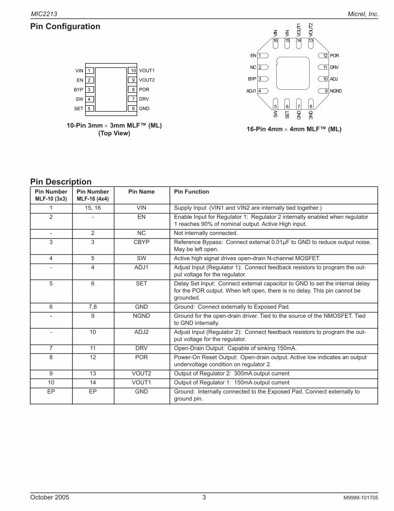
Pin Description Pin Number Pin Number Pin Name Pin Function MLF-10 (3x3) MLF-16 (4x4) 1 15, 16 VIN Supply Input (VIN1 and VIN2 are internally tied together.) 2 - EN Enable Input for Regulator 1: Regulator 2 internally enabled when regulator
1 reaches 90% of nominal output. Active High input. - 2 NC Not internally connected. 3 3 CBYP Reference Bypass: Connect external 0.01µF to GND to reduce output noise.
May be left open. 4 5 SW Active high signal drives open-drain N-channel MOSFET. - 4 ADJ1 Adjust Input (Regulator 1): Connect feedback resistors to program the out-
put voltage for the regulator. 5 6 SET Delay Set Input: Connect external capacitor to GND to set the internal delay
for the POR output. When left open, there is no delay. This pin cannot be grounded.
6 7,8 GND Ground: Connect externally to Exposed Pad. - 9 NGND Ground for the open-drain driver. Tied to the source of the NMOSFET. Tied
to GND internally. - 10 ADJ2 Adjust Input (Regulator 2): Connect feedback resistors to program the out-
put voltage for the regulator. 7 11 DRV Open-Drain Output: Capable of sinking 150mA. 8 12 POR Power-On Reset Output: Open-drain output. Active low indicates an output
undervoltage condition on regulator 2. 9 13 VOUT2 Output of Regulator 2: 300mA output current 10 14 VOUT1 Output of Regulator 1: 150mA output current EP EP GND Ground: Internally connected to the Exposed Pad. Connect externally to
ground pin.
1VIN
EN
BYP
SW
SET
10 VOUT1
VOUT2
POR
DRV
GND
9
8
7
6
2
3
4
5
10-Pin 3mm × 3mm MLF™ (ML) (Top View)
Pin Configuration
MIC2213 Micrel, Inc.
M9999-101705 4 October 2005
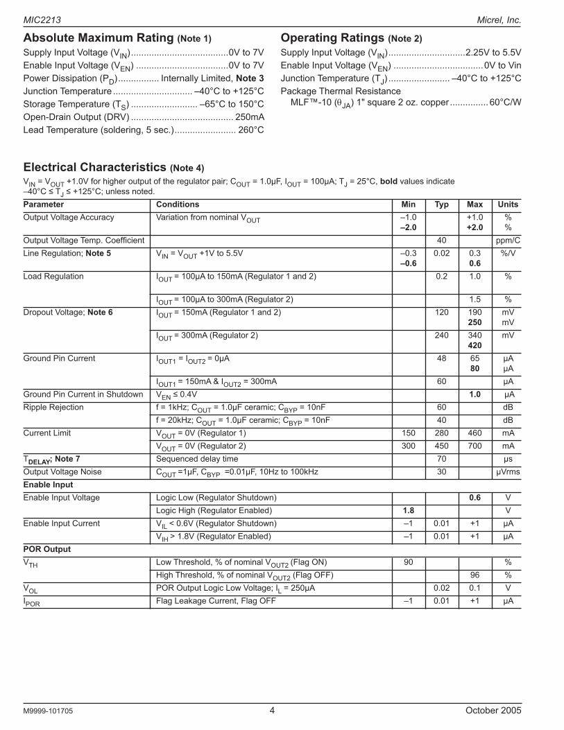
Electrical Characteristics (Note 4)VIN = VOUT +1.0V for higher output of the regulator pair; COUT = 1.0µF, IOUT = 100µA; TJ = 25°C, bold values indicate –40°C ≤ TJ ≤ +125°C; unless noted.Parameter Conditions Min Typ Max UnitsOutput Voltage Accuracy Variation from nominal VOUT –1.0 +1.0 % –2.0 +2.0 %Output Voltage Temp. Coefficient 40 ppm/CLine Regulation; Note 5 VIN = VOUT +1V to 5.5V –0.3 0.02 0.3 %/V –0.6 0.6Load Regulation IOUT = 100µA to 150mA (Regulator 1 and 2) 0.2 1.0 % IOUT = 100µA to 300mA (Regulator 2) 1.5 %Dropout Voltage; Note 6 IOUT = 150mA (Regulator 1 and 2) 120 190 mV 250 mV IOUT = 300mA (Regulator 2) 240 340 mV 420Ground Pin Current IOUT1 = IOUT2 = 0µA 48 65 µA 80 µA IOUT1 = 150mA & IOUT2 = 300mA 60 µAGround Pin Current in Shutdown VEN ≤ 0.4V 1.0 µARipple Rejection f = 1kHz; COUT = 1.0µF ceramic; CBYP = 10nF 60 dB f = 20kHz; COUT = 1.0µF ceramic; CBYP = 10nF 40 dBCurrent Limit VOUT = 0V (Regulator 1) 150 280 460 mA VOUT = 0V (Regulator 2) 300 450 700 mATDELAY; Note 7 Sequenced delay time 70 µsOutput Voltage Noise COUT =1µF, CBYP =0.01µF, 10Hz to 100kHz 30 µVrmsEnable InputEnable Input Voltage Logic Low (Regulator Shutdown) 0.6 V Logic High (Regulator Enabled) 1.8 VEnable Input Current VIL < 0.6V (Regulator Shutdown) –1 0.01 +1 µA VIH > 1.8V (Regulator Enabled) –1 0.01 +1 µAPOR OutputVTH Low Threshold, % of nominal VOUT2 (Flag ON) 90 % High Threshold, % of nominal VOUT2 (Flag OFF) 96 %VOL POR Output Logic Low Voltage; IL = 250µA 0.02 0.1 VIPOR Flag Leakage Current, Flag OFF –1 0.01 +1 µA
Absolute Maximum Rating (Note 1)Supply Input Voltage (VIN) ......................................0V to 7VEnable Input Voltage (VEN) ....................................0V to 7VPower Dissipation (PD) ................ Internally Limited, Note 3Junction Temperature ............................... –40°C to +125°CStorage Temperature (TS) .......................... –65°C to 150°COpen-Drain Output (DRV) ........................................ 250mALead Temperature (soldering, 5 sec.) ........................ 260°C
Operating Ratings (Note 2)Supply Input Voltage (VIN) ..............................2.25V to 5.5VEnable Input Voltage (VEN) ...................................0V to VinJunction Temperature (TJ) ........................ –40°C to +125°CPackage Thermal Resistance
MLF™-10 (θJA) 1" square 2 oz. copper ............... 60°C/W
October 2005 5 M9999-101705
MIC2213 Micrel, Inc.
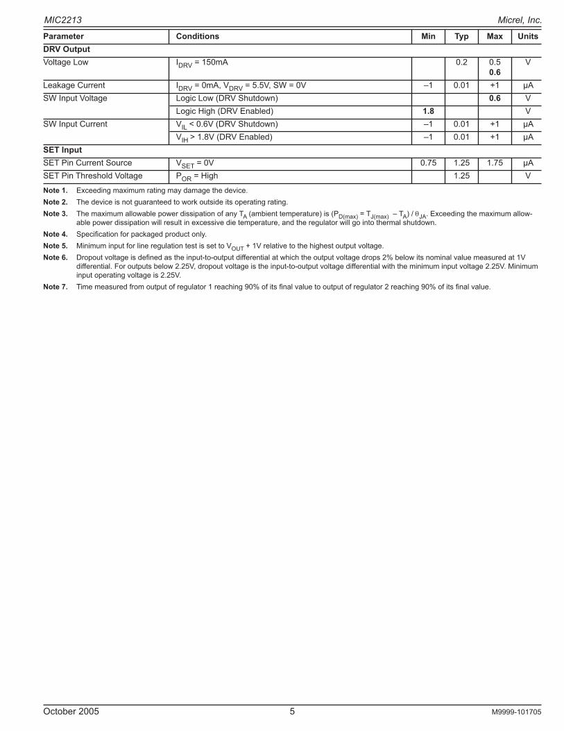
Parameter Conditions Min Typ Max UnitsDRV OutputVoltage Low IDRV = 150mA 0.2 0.5 V 0.6 Leakage Current IDRV = 0mA, VDRV = 5.5V, SW = 0V –1 0.01 +1 µASW Input Voltage Logic Low (DRV Shutdown) 0.6 V Logic High (DRV Enabled) 1.8 VSW Input Current VIL < 0.6V (DRV Shutdown) –1 0.01 +1 µA VIH > 1.8V (DRV Enabled) –1 0.01 +1 µASET InputSET Pin Current Source VSET = 0V 0.75 1.25 1.75 µASET Pin Threshold Voltage POR = High 1.25 V
Note 1. Exceeding maximum rating may damage the device.Note 2. The device is not guaranteed to work outside its operating rating.Note 3. The maximum allowable power dissipation of any TA (ambient temperature) is (PD(max) = TJ(max) – TA) / θJA. Exceeding the maximum allow-
able power dissipation will result in excessive die temperature, and the regulator will go into thermal shutdown. Note 4. Specification for packaged product only.Note 5. Minimum input for line regulation test is set to VOUT + 1V relative to the highest output voltage.Note 6. Dropout voltage is defined as the input-to-output differential at which the output voltage drops 2% below its nominal value measured at 1V
differential. For outputs below 2.25V, dropout voltage is the input-to-output voltage differential with the minimum input voltage 2.25V. Minimum input operating voltage is 2.25V.
Note 7. Time measured from output of regulator 1 reaching 90% of its final value to output of regulator 2 reaching 90% of its final value.
MIC2213 Micrel, Inc.
M9999-101705 6 October 2005
0
0.5
1
1.5
2
2.5
3
0 1 2 3 4 5SUPPLY VOLTAGE (V)
Dropout CharacteristicsOutput 1
150mA100µA
0
0.5
1
1.5
2
2.5
3
0 1 2 3 4 5SUPPLY VOLTAGE (V)
Dropout CharacteristicsOutput 2
300mA100µA
0
10
20
30
40
50
60
0 1 2 3 4 5 6SUPPLY VOLTAGE (V)
Ground Currentvs. Supply Voltage
Output 1 and 2with 100µA load
0
10
20
30
40
50
60
0 20 40 60 80 100 120 140OUTPUT 1 LOAD CURRENT (mA)
Ground Currentvs. Output 1 Current
0
10
20
30
40
50
60
0 50 100 150 200 250 300OUTPUT 2 LOAD CURRENT (mA)
Ground Currentvs. Output 2 Current
10E-9
100E-9
1E-6
10E-6
FREQUENCY (Hz)
Spectal NoiseDensity Output 1
COUT= 1µFC
IN= 1µF
CBYP = 0.01µF
100µA Load
10 100 1k 10k 100k 1M
10 100 1k 10k 100k 1M10E-9
100E-9
1E-6
10E-6
FREQUENCY (Hz)
Spectral NoiseDensity Output 2
100µA Load
COUT = 1µFC
IN= 1µF
CBYP = 0.01µF
0
20
40
60
80
0.01 0.1 1 10 100 1000FREQUENCY (kHz)
PSRR Output 2
CBYP = 10nF
CBYP = 100nF
CBYP = 1nF
VIN = VOUT + 1IOUT = 300mACOUT = 1µF
0
20
40
60
80
0.01 0.1 1 10 100 1000FREQUENCY (kHz)
PSRR Output 1
CBYP = 10nF
CBYP = 100nF
CBYP = 1nF
VIN = VOUT + 1IOUT = 150mACOUT = 1µF
0
50
100
150
-40 -20 0 20 40 60 80 100120140TEMPERATURE (°C)
Dropout VoltageOutput 1
150mA load
0
50
100
150
200
250
300
350
-40 -20 0 20 40 60 80 100120140TEMPERATURE (°C)
Dropout VoltageOutput 2
300mA load
0
10
20
30
40
50
60
-40
-20 0 20 40 60 80 100
120
140
160
TEMPERATURE (°C)
Ground Pin Current
Load on both outputs
0µA100µA
1mA
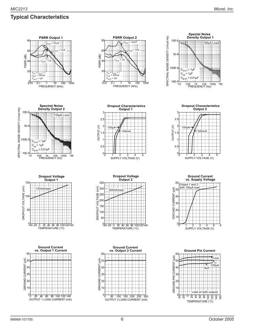
Typical Characteristics
October 2005 7 M9999-101705
MIC2213 Micrel, Inc.
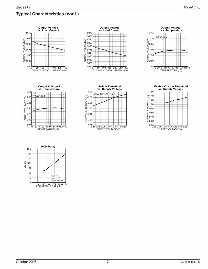
2.580
2.585
2.590
2.595
2.600
2.605
2.610
0 25 50 75 100 125 150OUTPUT 1 LOAD CURRENT (mA)
Output Voltagevs. Load Current
2.8202.8252.8302.8352.8402.8452.8502.8552.8602.8652.870
0 50 100 150 200 250 300OUTPUT 2 LOAD CURRENT (mA)
Output Voltagevs. Load Current
0.00
0.20
0.40
0.60
0.80
1.00
1.20
2.25 2.75 3.25 3.75 4.25 4.75 5.25SUPPLY VOLTAGE (V)
Switch Thresholdvs. Supply Voltage
Drive Current = 1mA
0.00
0.20
0.40
0.60
0.80
1.00
1.20
1.40
1.60
2.25 2.75 3.25 3.75 4.25 4.75 5.25SUPPLY VOLTAGE (V)
Enable Voltage Thresholdvs. Supply Voltage
2.85
2.90
2.95
3.00
3.05
3.10
3.15
-40 -20 0 20 40 60 80 100120140TEMPERATURE (°C)
Output Voltage 1vs. Temperature
100µA load
2.65
2.70
2.75
2.80
2.85
2.90
2.95
-40 -20 0 20 40 60 80 100120140TEMPERATURE (°C)
Output Voltage 2vs. Temperature
100µA load
Typical Characteristics (cont.)
POR SETTING CAP (pF)
POR Delay
CIN = 1µFC = 1µFILOAD = 100µA
1 10 100 1k 10k 100k 1M1
10
100
1k
10k
100k
10M
1M
OUT
MIC2213 Micrel, Inc.
M9999-101705 8 October 2005
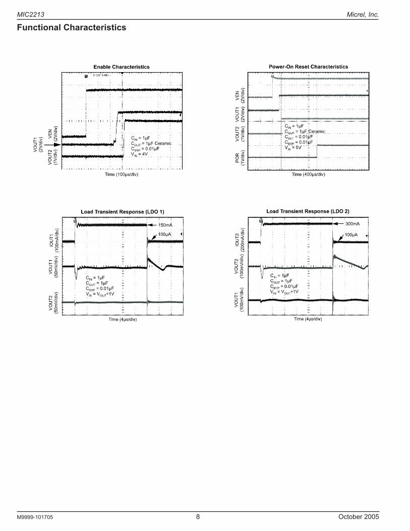
Functional Characteristics
October 2005 9 M9999-101705
MIC2213 Micrel, Inc.
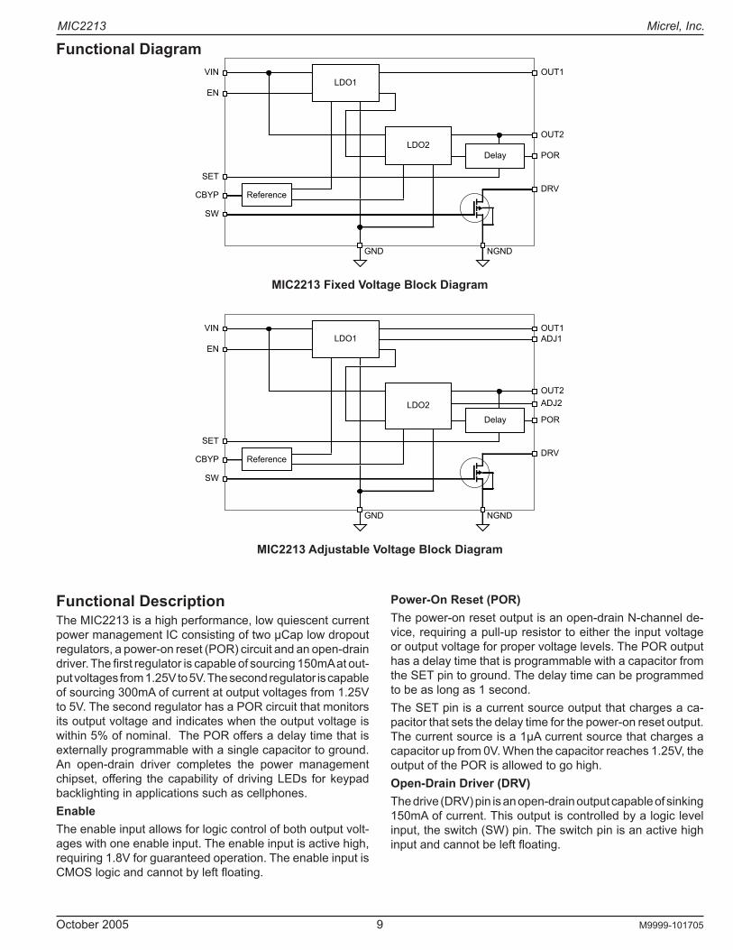
Functional DiagramOUT1
OUT2
POR
DRV
NGNDGND
SW
CBYP
SET
EN
VINLDO1
LDO2
Reference
Delay
MIC2213 Fixed Voltage Block Diagram
OUT1
OUT2
POR
DRV
NGNDGND
SW
CBYP
SET
EN
VIN
ADJ2
ADJ1LDO1
LDO2
Reference
Delay
MIC2213 Adjustable Voltage Block Diagram
Functional DescriptionThe MIC2213 is a high performance, low quiescent current power management IC consisting of two µCap low dropout regulators, a power-on reset (POR) circuit and an open-drain driver. The first regulator is capable of sourcing 150mA at out-put voltages from 1.25V to 5V. The second regulator is capable of sourcing 300mA of current at output voltages from 1.25V to 5V. The second regulator has a POR circuit that monitors its output voltage and indicates when the output voltage is within 5% of nominal. The POR offers a delay time that is externally programmable with a single capacitor to ground. An open-drain driver completes the power management chipset, offering the capability of driving LEDs for keypad backlighting in applications such as cellphones.Enable The enable input allows for logic control of both output volt-ages with one enable input. The enable input is active high, requiring 1.8V for guaranteed operation. The enable input is CMOS logic and cannot by left floating.
Power-On Reset (POR)The power-on reset output is an open-drain N-channel de-vice, requiring a pull-up resistor to either the input voltage or output voltage for proper voltage levels. The POR output has a delay time that is programmable with a capacitor from the SET pin to ground. The delay time can be programmed to be as long as 1 second.The SET pin is a current source output that charges a ca-pacitor that sets the delay time for the power-on reset output. The current source is a 1µA current source that charges a capacitor up from 0V. When the capacitor reaches 1.25V, the output of the POR is allowed to go high. Open-Drain Driver (DRV)The drive (DRV) pin is an open-drain output capable of sinking 150mA of current. This output is controlled by a logic level input, the switch (SW) pin. The switch pin is an active high input and cannot be left floating.
MIC2213 Micrel, Inc.
M9999-101705 10 October 2005
Input CapacitorGood bypassing is recommended from input to ground to help improve AC performance. A 1µF capacitor or greater located close to the IC is recommended.Bypass CapacitorThe internal reference voltage of the MIC2213 can be by-passed with a capacitor to ground to reduce output noise and increase power supply rejection (PSRR). A quick-start feature allows for quick turn-on of the output voltage regardless of the size of the capacitor. The recommended nominal bypass capacitor is 0.01µF, but it can be increased without limit. Output CapacitorEach regulator output requires a 1µF ceramic output capaci-tor for stability. The output capacitor value can be increased to improve transient response, but performance has been optimized for a 1µF ceramic type output capacitor.X7R/X5R dielectric-type ceramic capacitors are recom-mended because of their temperature performance. X7R-type capacitors change capacitance by 15% over their operating temperature range and are the most stable type of ceramic capacitors. Z5U and Y5V dielectric capacitors change value by as much as 50% and 60% respectively over their operat-ing temperature ranges. To use a ceramic chip capacitor with Y5V dielectric, the value must be much higher than a X7R ceramic capacitor to ensure the same minimum capacitance over the equivalent operating temperature range.
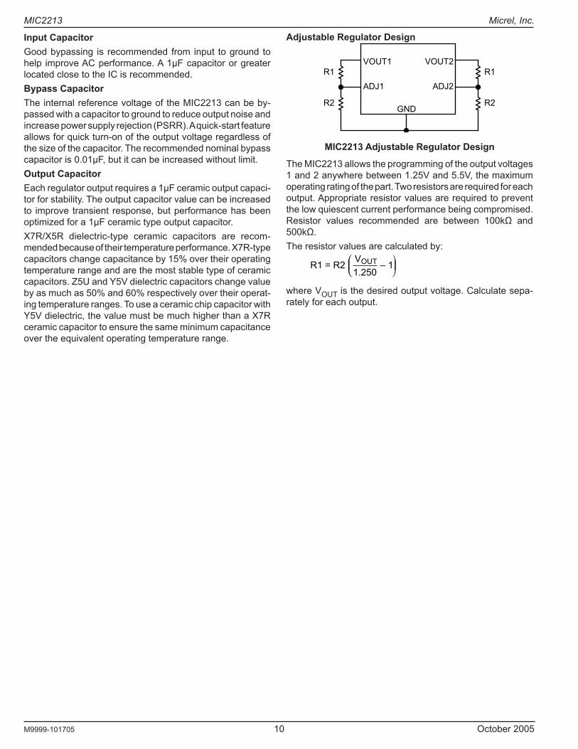
Adjustable Regulator Design
VOUT1
ADJ1
R1
R2
ADJ2
VOUT2
R2
R1
GND
MIC2213 Adjustable Regulator Design
The MIC2213 allows the programming of the output voltages 1 and 2 anywhere between 1.25V and 5.5V, the maximum operating rating of the part. Two resistors are required for each output. Appropriate resistor values are required to prevent the low quiescent current performance being compromised. Resistor values recommended are between 100kΩ and 500kΩ.The resistor values are calculated by:
R1 = R2
1.250– 1VOUT
where VOUT is the desired output voltage. Calculate sepa-rately for each output.
October 2005 11 M9999-101705
MIC2213 Micrel, Inc.
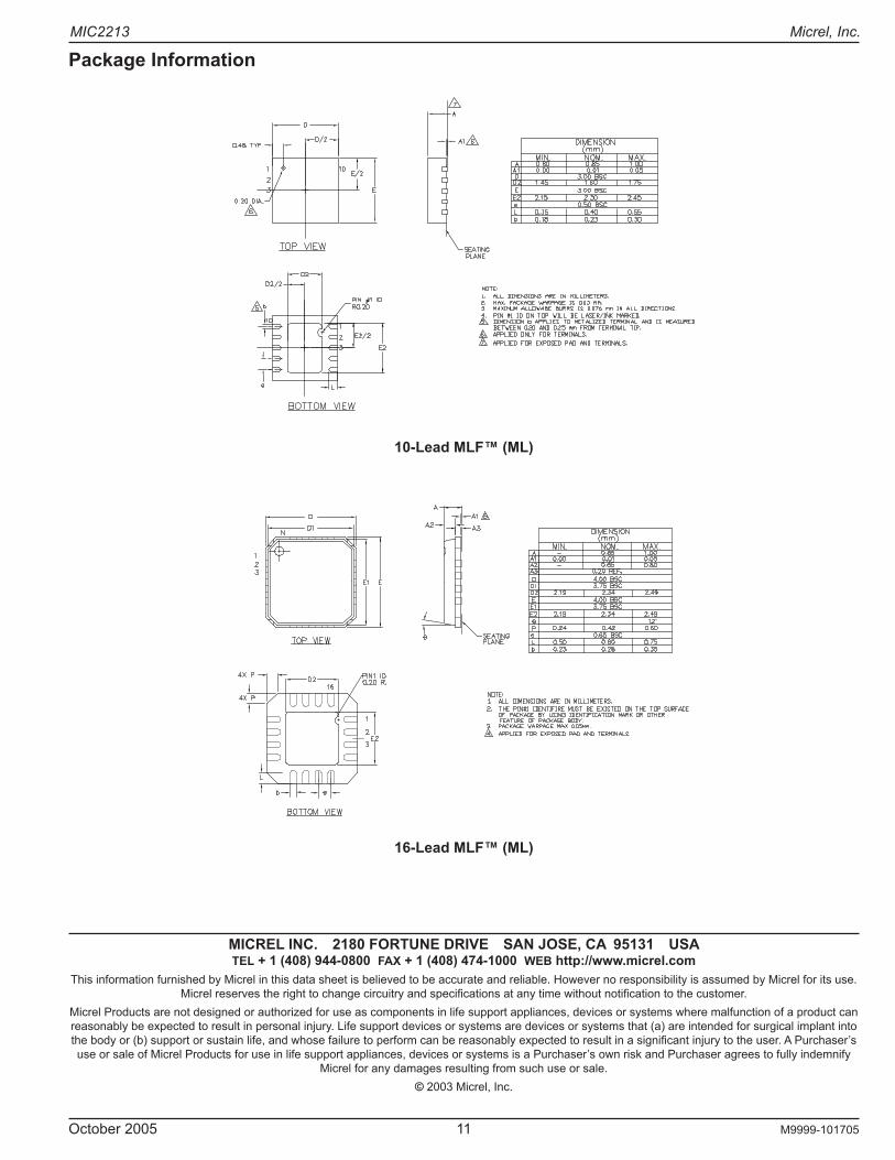
Package Information
10-Lead MLF™ (ML)
16-Lead MLF™ (ML)
MICREL INC. 2180 FORTUNE DRIVE SAN JOSE, CA 95131 USATEL + 1 (408) 944-0800 FAX + 1 (408) 474-1000 WEB http://www.micrel.com
This information furnished by Micrel in this data sheet is believed to be accurate and reliable. However no responsibility is assumed by Micrel for its use. Micrel reserves the right to change circuitry and specifications at any time without notification to the customer.
Micrel Products are not designed or authorized for use as components in life support appliances, devices or systems where malfunction of a product can reasonably be expected to result in personal injury. Life support devices or systems are devices or systems that (a) are intended for surgical implant into the body or (b) support or sustain life, and whose failure to perform can be reasonably expected to result in a significant injury to the user. A Purchaser’s use or sale of Micrel Products for use in life support appliances, devices or systems is a Purchaser’s own risk and Purchaser agrees to fully indemnify
Micrel for any damages resulting from such use or sale.© 2003 Micrel, Inc.