Ferroelectret Ultrasonic Transducers for Pulse-Echo Water ...

1
MEMS ultrasonic transducers for the testing of solids
Abstract—Arrays of capacitive diaphragm ultrasonic transducers could potentially be used for non-destructive
ultrasonic testing and structural monitoring. In this paper, we consider the efficiency of coupling of these transducers to
solid media. We show that efficient coupling can be realized by using a silicone coating as a coupling medium. We
present the results of experimental characterization of ultrasonic transducers coupled to solids in this way. We show that
these transducers can be used with piezoelectric emitting transducers within the range from 1 to 5 MHz and we
demonstrate the use of several transducers as a phased array in order to determine the direction and distance of an
ultrasonic source.
Index Terms—capacitive diaphragm, micromachined, transducer, ultrasonic
I. INTRODUCTION
ETAL structures such as bridges, building frameworks, and piping can fail because of fatigue crack
propagation or because of section loss from corrosion. Regular inspection is required to detect such failures.
Among the variety of inspection techniques available, ultrasonic flaw detection is attractive for the early detection of
cracks and other critical flaws. We seek to develop MEMS-based transducers for ultrasonic flaw detection, to be
permanently mounted at critical locations on structures. In a complete inspection system, phased array emission or
detection will be necessary so that a single fixed sensor can detect flaws within a significant volume of material.
In this paper, we examine experimentally the performance of transducers for this application. In particular we
consider the critical issue of coupling of the ultrasonic energy from the emitting and receiving transducers to the
solid structural elements. Understanding of the coupling is crucial in design of the sensor system. We will show
that a single piezoelectric emitter together with a phased array consisting of several MEMS receivers is the most
attractive sensor architecture. We will then report initial characterization of MEMS ultrasonic transducers that are
coupled to a solid medium. It will be shown that transducers can be efficiently coupled to a solid medium. We also
will demonstrate the operation of a MEMS phased array, including the determination of the distance and angular
location of an ultrasonic emitter. Finally, we will outline the factors that limit the sensitivity of our present
I.J. Oppenheim, A. Jain, and D.W. Greve, Member, IEEE
M
2
transducer design, and describe improvements to be made in future designs.
MEMS ultrasonic transducers are very attractive for a permanently attached sensor system because of the
potential for low cost. The potential for low cost derives from the fact that a sensor array several acoustic
wavelengths in extent can be fabricated on a silicon chip of reasonable size (1 cm2) that could contain both sensors
and electronic circuitry. We focus here on capacitive diaphragm transducers, that can be made using materials
already available in surface micromachined processes. There has been a significant amount of prior published work
that has generally concerned transducers coupled to air or fluids [1,2,3,4]. Other work has also demonstrated the
potential applications of these fluid-coupled transducers in imaging arrays [5,6]. The first steps toward the
application of these transducers to testing of solids was recently taken by Khuri-Yakub and coworkers, who
demonstrated the transmission of an ultrasonic pulse through an aluminum sheet using a capacitive diaphragm
transducer as both transmitter and receiver [7]. The generated ultrasonic wave was coupled to the sheet by air gaps.
In this paper, we consider various potential combinations of ultrasonic transmitter and receiver and different
methods of coupling the ultrasonic wave. As our objective is to scan a significant volume of material with a fixed
device, at least one transducer must be of the array type. We assume that MEMS transducers are used for the array
as the complexity and cost of fabrication of piezoelectric arrays appears to be prohibitive in this application. The
design choice is thus between a MEMS array as transmitter or receiver; the other (single) transducer can be either a
MEMS device or a piezoelectic element. An additional design decision is the method of coupling from the MEMS
device to the solid object to be monitored.
1. EMISSION OF ULTRASONIC ENERGY INTO SOLID
Figure 1 shows an equivalent circuit for an ultrasonic transmitter. This equivalent circuit appears, for example, in
Berlincourt et al. [8] and applies to both capacitive and piezoelectric transducers. Under open-circuit output
conditions (transducer coupled to a medium with acoustic impedance Zm = infinity), the turns ratio n relates the
voltage at the tranducer input to force per unit area on the medium, that is
nvPSF
== (1)
where P [nt/m2] is the pressure, S [m2] is the transducer area, and v [V] is the applied voltage. In the case of
piezoelectric transducer the turns ratio n [coul/m3] is given by [8]
lhnpiezo
ε33= (2)
3
where ε is the dielectric constant, h33 [V/m] is the piezoelectric deformation constant, and l [m] is the transducer
thickness. For a capacitive transducer we have [9]
20
)( xgVn DC
MEMS −=
ε (3)
where VDC is the applied bias voltage, g is the gap, and x is the displacement due to the DC bias. The predicted
turns ratio for a piezoelectric transducer depends on the particular material chosen and the resonant frequency. For a
lead zirconium titanate transducer of thickness 0.5 mm it is approximately 64000 coul/m3 = 64000 nt/m2⋅V [8]. The
turns ratio for a MEMS capacitive transducer depends on both the physical parameters and the applied DC bias. For
a small gap and high bias voltage it is possible for nMEMS to exceed that for a piezoelectric transducer. However, this
requires very high electric fields and probably also a diaphragm operating near the collapse condition. For more
moderate operating conditions (E = 108 V/m and g-x = 1.5 µm) a turns ratio of order 590 coul/m3 is predicted.
It also worth observing that MEMS capacitive transducers have usually been operated in either air or fluids. We
now consider the coupling between a MEMS operating in air or a fluid to a solid. We suppose that the MEMS
transducer creates a pressure wave of amplitude Pi in a medium with acoustic impedance Zi [kg/m2s]. The pressure
amplitude Pm in the solid medium is
iiim
mm PP
ZZZP 22
≈+
= (4)
While the pressure in the solid is doubled, the energy density in the solid is much reduced. In general the energy
density ZPE ρ2/2= where ρ is the mass density and Z is the acoustic impedance. Consequently the ratio of energy
coupled into the medium to the emitted energy is given by
14 <<=mm
ii
ZZr
ρρ . (5)
As the MEMS capacitive transducer is considerably less effective under conservative operating conditions, we
have chosen to use a single PZT emitter and an array of MEMS capacitive diaphragm receivers. The remaining
issue, then, is the coupling between the solid medium and the MEMS receivers.
2. COUPLING OF ULTRASONIC ENERGY FROM SOLID INTO TRANSDUCER
In previous work, Ladabaum and coworkers [9] studied ultrasonic transmission from an aluminum plate and
through an air gap to an MEMS receiver. Here we compare quantitatively the efficiency of coupling through an air
gap to the efficiency using a coupling medium such as silicone. The relevant transmission line equivalent circuit is

4
shown in Fig. 2.
We consider first a receiving transducer that is coupled to through an air gap to a solid material. As the ultrasonic
wavelength in air is quite small (λ = 94 µm at 3.5 MHz) it is likely that any gap obtained by mechanical alignment
will be several wavelengths. In the previous work by Ladabaum et al. [9] the gap was very large (1 cm). When the
transducer is used for flaw detection the emitted ultrasonic pulse must be short in order to obtain good resolution,
typically only a few cycles at the transducer resonant frequency. If this is the case, interference can be neglected,
and the amplitude of the pressure wave emitted from the solid into the air gap is given by
im
airi
airm
airair P
ZZ
PZZ
ZP
22≈
+= (6)
where Pi is the amplitude of the incident wave, and Zair and Zm the acoustic impedance of air and the transmitting
media, respectively. When the pulse reaches the detector, the diaphragm velocity will be
im
air
tair
PZZ
ZZu
22+
= (7)
where Zt is the diaphragm acoustic impedance. This can be compared with the ideal case in which a diaphragm with
negligible acoustic impedance is rigidly coupled to the solid surface. In this case the diaphragm velocity is equal to
the velocity of the free surface which is mi ZPu /2= ; consequently we can define a coupling gain
t
air
ZZ
gain2
= . (8)
In Fig. 3 we plot the transducer impedance as a function of frequency using the parameters of a single-degree-of-
freedom model developed from electrical measurements on fabricated transducers [10]. The dashed curve includes
the effect of air damping through etch holes as this damping mechanism is present when the detector is operated
exposed to air. We observe that Zt > Zair even at the detector resonant frequency. Consequently the coupling gain is
at best equal to 0.81 exactly at the detector resonant frequency, and lower when operated away from the detector
resonant frequency. A further disadvantage of air coupling is the degradation of time resolution if the transducer has
a high Q when operated in air.
In contrast, we now consider the coupling gain through a thin layer of silicone as we have previously reported
[10]. We have measured the acoustic parameters for Gelest Zipcone CG silicone as c = 1300 m/s and Zsilicone =
150000 kg/m2s.
In our experiments, the measured thickness of the coupling layer is approximately 20 µm, compared to an
acoustic wavelength of approximately 540 µm at 5 MHz. As the coupling layer thickness is less than an acoustic

5
wavelength, it is appropriate to calculate the coupling gain using the transmission line equations including
interference effects within the coupling layer. In this case the transducer impedance Zt is small compared to the
silicone impedance (Fig. 3) and as a result the termination is essentially a short circuit. Calculations show that the
coupling gain in this case is given by
−+= )
2(sin11 2
2
2
silicone
silicone
m
silicone tZ
Zgain
λπ (9)
where tsilicone and λsilicone are the silicone thickness and acoustic wavelength, respectively. The gain predicted by eq.
(9) becomes unity when the silicone thickness is much smaller than the acoustic wavelength. This is a substantial
improvement over the coupling obtained through a multiple-wavelength air gap.
3. OUTPUT VOLTAGE
The output voltage can be computed using the equivalent circuit of Fig. 4, where Cp represents the parasitic
capacitance between the output node and ground. We have
dtdx
gSV
dtdvC
dtdCv
dtdvCi DC 2
0ε+=+= 00 (9)
and since u = dx/dt and assuming that the input resistance of the amplifier is large, we obtain
uCC
Cjg
Vvp
DCo
0
0
+=
ω1 (10)
Note that the expected signal is proportional to the DC bias voltage and that it is severely degraded when Cp > C0.
EXPERIMENTAL
The multi-user MUMPS process [11] was used to fabricate capacitive diaphragm transducers, each consisting of
180 individual diaphragms in parallel. MUMPS is a surface-machined MEMS process with three polysilicon levels
(POLY0, POLY1, and POLY2). Briefly, the diaphragms were formed between POLY0 and POLY1 layers, with the
POLY0 plate in the form of a hexagon with an edge of 45 µm. The diaphragm thickness and spacing were fixed by
the fabrication process and were nominally 2 µm. A CAD layout of the chip and a cross-section of a completed
diaphragm are shown in Fig. 5, and essential dimensions are presented in Table I. The 1 cm × 1 cm chip consisted
of an array of nine transducers arranged in a linear array at one edge of the chip with the bonding pads at the other
edge of the chip. Details of the release process and the diaphragm design are reported in [10]. Because of a
particularly conservative design of the anchors, the parasitic capacitance between the diaphragm electrodes and
ground was large (96 pF for the POLY1 electrode and 151 pF for the POLY0 electrode.) The back surface of the
6
chip was etched, metallized, and grounded during the measurements described below.
The chip was bonded to a plexiglas test specimen by applying Gelest Zipcone CG silicone coating [12] using a
brush and then carefully placing the chip on the plexiglas. After drying few small (~ 50 µm diameter) bubbles were
observed, covering less than 5% of the total detector area and eight of the transducers were operational.
Capacitance-voltage measurements at 1 MHz showed that the operational transducers were electrically identical and
the diaphragm deflection deduced from C(V) measurements was less than unbonded devices, consistent with
successful bonding of the diaphragm top surface to the plexiglas [10]. There may be alternative materials or
combinations of bonding materials that are more convenient or that give higher yield of bonded detectors. This
could be addressed in future studies. According to eq. (9), any material that can be applied in a thin layer and that
has an acoustic impedance substantially higher than the diaphragm will provide for efficient coupling.
A Krautkramer MSW-QC ultrasonic transducer was coupled to the plexiglas specimen and driven by a
Krautkramer USPC-2100. Transducers with various resonant frequencies were used (1 MHz, 3.5 MHz, and 5
MHz). As shown in Fig. 6, the transducer could be attached in different locations in order to provide for uniform
illumination (not shown) or off-axis incident illumination with various source distances and incidence angles.
Individual detectors were contacted using a standard probe station. The output signal was recorded using an HP
54601A oscilloscope triggered by the pulse exciting the PZT transducer. The additional parasitic capacitance
contributed by the oscilloscope input plus the connecting cable was approximately 180 pF. The oscilloscope was
used in the averaging mode (256 or 1024 transients). The recorded waveforms were subsequently transferred to a
PC running Labview, and additional data processing (bandpass filtering using a rectangular frequency window) was
performed off-line using Mathcad software. In the phased-array experiments discussed below, multiple transducer
signals were recorded one at a time without changing the oscilloscope trigger parameters. Multiple signals from the
phased array were subsequently combined during off-line analysis.
TRANSDUCER OPERATION
We first verified the transducer operation and examined the transducer response at three different frequencies.
Figure 7 shows the observed signals as a function of DC bias voltage on the detectors for an ultrasonic pulse
uniformly incident on all detectors (transmitter 1.35 cm from the detector chip, not shown in Figure 6). The emitted
pulse is at t = 1 µs and a signal is observed at t = 1 µs due to stray electrical coupling even with zero DC bias. A
received pulse appears only when a DC bias is applied and is approximately linearly dependent on the DC bias as
expected. The received pulse occurs approximately 4.9 µs after the emitted pulse, which is in good agreement with
7
the delay of 5.0 µs predicted using the velocity of sound in plexiglas (c = 2700 m/s). (The bottom trace shows the
result of a point-by-point subtraction of the signals with VDC = 0 V and VDC = 100 V. This confirms that the signal at
t = 1 µs is due to electrical coupling.)
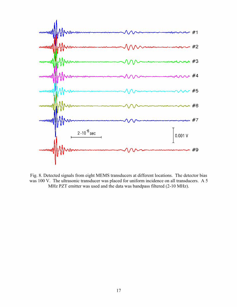
Figure 8 shows the signals obtained from several different detectors for this same uniform incidence arrangement.
In all cases a received pulse is observed at approximately 4.9 µs after the exciting pulse. In addition there is weaker
pulse consistently observed at approximately 8 µs delay. This pulse can be explained by reflection from one of the
surfaces of the prism.
In Figure 9 we show the result of measurements for the normal incidence condition using three different emitting
transducers resonant at three different frequencies. Observable signals are obtained from all three transducers,
suggesting that the diaphragm detectors have a wide bandwidth. This is consistent with the discussion of coupling
presented above. Large bandwidth is expected because the diaphragm impedance is small compared to the acoustic
impedance of the materials that couple the acoustic energy (silicone and plexiglas in the experiments described
here).
As noted earlier, we envision the use of an array of MEMS ultrasonic transducers that are used to scan a critical
member for cracks that are indicative of potential structural failure. In such an application detectors are operated as
a phased array. In this section, we demonstrate the use of a fixed array to determine the distance and angular
location of an ultrasonic source.
Figure 10 shows the results obtained for an emitting transducer in location A of Figure 6. Transducers are
numbered beginning with the left hand edge so the transducer nearest to this source is #1 and the most distant is #9.
Received signals are observed for all operational detectors with approximately the same amplitude. As expected, we
observe increasing delay moving from #1 to #9. (Transducer #4 was initially non-functional and transducer #8
failed or was damaged in the course of measurements). The delay between transducers is given by
cdt )cos(θ
=∆ (11)
where d = 990 µm is the spacing between transducers and θ is the angle measured with respect to the horizontal.
Figure 9 illustrates the determination of the delay time between transducers. We plot a sum of delayed signals given
by
∑ ⋅−=n
n ntvtV )(),( ττ (12)
where vn(t) is the signal from the nth transducer and τ is the delay. This results in a summed signal that depends on

8
the delay time τ. These summed signals are plotted in Figure 11 as a function of the delay time. We observe that
the transducer signals add coherently to give the largest summed signal for τ = 320 ns. This yields θ = 29 degrees,
in reasonable agreement with the prism shape. The total delay of the pulse corresponding to the transducer #5 (the
center transducer) is approximately 9.7 µs. Subtracting the trigger delay time of 1 µs, this corresponds to a distance
to the source of 2.35 cm, in excellent agreement with the prism shape.
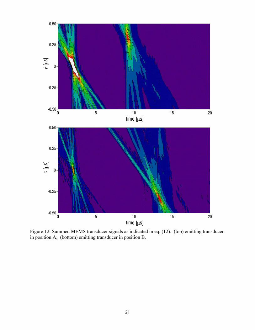
Localization of a source by phased-array detection can be illustrated more vividly by making a contour plot of
|V(t,τ)|. On this contour plot the angular position of a source is related to the peak position on the τ axis while the
distance is proportional to the peak location on the t axis. Figure 12 shows these contour plots for the two detector
locations indicated in Figure 6. Note that times should be measured with respect to the origin determined by the
source delay (t = 2 µs, τ = 0). The data clearly show that emitter location A is more distant from the leftmost
detector than emitter location B, and that τ is negative for location B as expected.
CONCLUSIONS
We have presented here progress toward the development of a MEMS-based ultrasonic sensor that can
permanently mounted in crucial structural locations. We have shown that MEMS capacitive transducers can be
successfully bonded to solids. The approach we have used (bonding with silicone) offers good acoustic coupling
and does not damage the transducers. We have also demonstrated the use of multiple MEMS detectors to form a
phased array that can detect the direction and distance of an ultrasonic source.
It needs to be recognized, however, that signal levels in these experiments have been low. The low signal levels
have two causes. First, there is a considerable decrease in signal level that results from the stray capacitance
between the output terminal and ground. In these measurements the stray capacitance was approximately 276 pF
leading according to eq. (1) to a reduction in output voltage of approximately two orders of magnitude. This signal
loss can be greatly ameliorated by a more optimum design of the anchors and also by using an integrated or lower-
capacitance preamplifier. Secondly, the diaphragm gap is large (2.0 µm). An appreciable decrease in the gap is
possible in the MUMPS process by using the DIMPLE mask and an additional decrease will be possible in a custom
process. These changes will lead to a practical transducer that will be appropriate for the permanently fixed sensor
that we have described.
ACKNOWLEDGMENT
This work has been funded by the Commonwealth of Pennsylvania through the Pennsylvania Infrastructure

9
Technology Alliance program, administered at Carnegie Mellon by the Institute for Complex Engineering Systems,
and by gifts from Krautkramer Inc.

10
TABLE CAPTIONS Table 1. Dimensions and other parameters for the diaphragm transducer.
FIGURE CAPTIONS
Figure 1. Equivalent circuit of a piezoelectric transducer.
Figure 2. Equivalent circuit for coupling between a solid medium with acoustic impedance Zm and a detector with
acoustic impedance Zt.
Figure 3. Magnitude of the acoustic impedance for a MEMS transducer calculated using parameters of the single-
degree-of-freedom model.
Figure 4. Equivalent circuit for evaluation of the output voltage.
Figure 5. MEMS ultrasonic transducers: (top) CAD layout of the chip (1 cm × 1 cm) and (bottom) cross section of
one diaphragm.
Figure 6. Drawing showing plexiglas test speciment with two off-axis locations for the emitting transducer.
Figure 7. Detected signal from MEMS transducer as a function of bias voltage. A 3.5 MHz PZT emitting
transducer was used and the data was bandpass filtered with cutoffs at 2 MHz and 10 MHz.
Figure 8. Detected signals from eight MEMS transducers at different locations. The detector bias was 100 V. The
ultrasonic transducer was placed for uniform incidence on all transducers. A 5 MHz PZT emitter was used and the
data was bandpass filtered (2-10 MHz).
11
Figure 9. Detected signals from one MEMS transducer as a function of emitting transducer frequency. The detector
bias was 100 V. The data was filtered with different bandpass depending upon the transducer frequency: 1 MHz
transducer (0.3-10 MHz); 3.5 MHz transducer (1.7-7 MHz); and 5 MHz transducer (2.5-10 MHz).
Figure 10. Detected signals from seven MEMS transducers at different locations. The detector bias was 100 V.
The emitting transducer was placed at location A in Figure 6. A 3.5 MHz PZT emitter was used and the data was
bandpass filtered (1.7-7 MHz).
Figure 11. Sum of time-shifted signals from seven MEMS transducers as a function of delay time τ. The detector
bias was 100 V and the emitting transducer was placed at location A in Figure 6. A 3.5 MHz PZT emitter was used
and the data was bandpass filtered (1.7-7 MHz).
Figure 12. Summed MEMS transducer signals as indicated in eq. (12): (top) emitting transducer in position A;
(bottom) emitting transducer in position B.
12
REFERENCES
1 P.-C. Eccardt, K. Niederer, T. Scheiter, and C. Hierold, "Surface micromachined ultrasound transducers in CMOS
technology," 1996 IEEE Ultrasonics Symposium Proc., pp. 959-962 (1996).
2 A.G. Bashford, D.W. Schindel, D.A. Hutchins, "Micromachined ultrasonic capacitance transducers for immersion
applications," IEEE Transactions on Ultrasonics, Ferroelectrics, and Frequency Control, vol. 45, pp. 367-375
(1998).
3 X. Jin, I. Ladabaum, F.L. Degertekin, S. Calmes, and B.T. Khuri-Yakub, "Characterization of one-dimensional
capacitive micromachined ultrasonic immersion transducer arrays," IEEE Journal of Microelectromechanical
Systems, vol. 8, pp. 100-114 (1999).
4 X. Jin, O. Oralkan, F.L. Degertekin, and B.T. Khuri-Yakub, "Characterization of one-dimensional capacitive
micromachined ultrasonic immersion transducer arrays," IEEE Transactions on Ultrasonics, Ferroelectrics, and
Frequency Control, vol. 48, pp. 750-760 (2001).
5 O. Oralkan, X.C. Jin, K. Kaviani, A.S. Ergun, F.L.Degertekin, M. Karaman, and B.T. Khuri-Yakub, "Initial pulse-
echo imaging results with one-dimensional capacitive micromachined ultrasonic transducer arrays," 2000 IEEE
Ultrasonics Symposium Proc., pp. 959-962 (2000).
6 P.-C. Eccardt, K. Niederer, and B. Fischer, "Micromachined transducers for ultrasound applications," 1997 IEEE
Ultrasonics Symposium Proc., pp. 1609-1618 (1997).
7 S.T. Hansen, B.J. Mossawir, A.S. Ergun, F. L. Degertekin, and B.T. Khuri-Yakub, "Air-coupled nondestructive
evaluation using micromachined ultrasonic transducers," 1999 IEEE Ultrasonics Symposium Proc., pp. 1037-1040
(1999).
8 D.A. Berlincourt, D.R. Curran, and H. Jaffe, "Piezoelectric and Piezomagnetic Materials and their Function in
Transducers," pp. 233-250, in Physical Acoustics, vol. 1, (ed. W.P. Mason, Academic Press, London, 1964).
9 I. Ladabaum, X. Jin, S.T. Soh, A. Atalar, and B.T. Khuri-Yakub, "Surface Micromachined Capacitive Ultrasonic
Transducers," IEEE Trans. Ultrasonics, Ferroelectrics, and Frequency Control, vol. 45, pp. 678-690, May 1998.
10 I.J. Oppenheim, A. Jain, and D.W. Greve, "Electrical characterization of coupled and uncoupled MEMS ultrasonic
transducers," (submitted for publication).
11 Details of the MUMPS process are available from JDS Uniphase, MEMS Business Unit (Cronos), 3026
Cornwallis Road, Research Triangle Park, NC 27709 at also from http://www.memsrus.com/mumps.pdf.
12 Gelest, Inc., 11 East Steel Road, Morrisville, PA 19067.

13
Table 1. Dimensions and other parameters for the diaphragm transducer.
material thickness area top diaphragm electrode polysilicon 2 µm 6260 µm2
bottom diaphragm electrode polysilicon 0.5 µm 3650 µm2 inter-electrode gap air 2 µm -
14
ZmC0
1:n
Vacejωt+
transducer
Figure 1. Equivalent circuit of a piezoelectric transducer.
Zt
Zm
Pi
Zc
u
Figure 2. Equivalent circuit for coupling between a solid medium with acoustic impedance Zm and a detector with acoustic impedance Zt.
Figure 3. Magnitude of the acoustic impedance for a MEMS transducer calculated using parameters of the single-degree-of-freedom model.
silicone line should be moved down

15
+vo
C0
n:1
VDC
Rin
i
P⋅S
u
Cp
–+
Fig. 4. Equivalent circuit for evaluation of the output voltage.
Figure 5. MEMS ultrasonic transducers: (top) CAD layout of the chip (1 cm × 1 cm) and (bottom) cross section of one diaphragm.

16
25°
2.3 cm
21°2.6 cm
24° bonded transducer chip
PZT ultrasonic transducer
A B
Fig. 6. Drawing showing plexiglas test speciment with two off-axis locations for the emitting transducer.
Fig. 7. Detected signal from MEMS transducer as a function of bias voltage. A 3.5 MHz PZT emitting transducer was used and the data was bandpass filtered with cutoffs at 2 MHz and 10
MHz.
17
Fig. 8. Detected signals from eight MEMS transducers at different locations. The detector bias was 100 V. The ultrasonic transducer was placed for uniform incidence on all transducers. A 5
MHz PZT emitter was used and the data was bandpass filtered (2-10 MHz).

18
Fig. 9. Detected signals from one MEMS transducer as a function of emitting transducer frequency. The detector bias was 100 V. The data was filtered with different bandpass
depending upon the transducer frequency: 1 MHz transducer (0.3-10 MHz); 3.5 MHz transducer (1.7-7 MHz); and 5 MHz transducer (2.5-10 MHz).

19
Figure 10. Detected signals from seven MEMS transducers at different locations. The detector bias was 100 V. The emitting transducer was placed at location A in Figure 6. A 3.5 MHz PZT
emitter was used and the data was bandpass filtered (1.7-7 MHz).

20
Figure 11. Sum of time-shifted signals from seven MEMS transducers as a function of delay time τ. The detector bias was 100 V and the emitting transducer was placed at location A in Figure 6. A 3.5 MHz PZT emitter was used and the data was bandpass filtered (1.7-7 MHz).
21
Figure 12. Summed MEMS transducer signals as indicated in eq. (12): (top) emitting transducer in position A; (bottom) emitting transducer in position B.