memo-466
26
CSAIL Massachusetts Institute of Technology Identification and Authentication of Integrated Circuits Blaise Gassend, Dwaine Clarke, Daihyun Lim, Marten van Dijk, Srini Devadas To appear in Concurrency and Computation: Practice and Experience, Wiley, 2003 2003, June Computation Structures Group Memo 466 The Stata Center, 32 Vassar Street, Cambridge, Massachusetts 02139 Computer Science and Artificial Intelligence Laboratory
-
Upload
olivier-ouina -
Category
Documents
-
view
219 -
download
2
description
MEMO
Transcript of memo-466

CSAIL Massachusetts Institute of Technology
Identification and Authentication of Integrated Circuits
Blaise Gassend, Dwaine Clarke, Daihyun Lim,
Marten van Dijk, Srini Devadas
To appear in Concurrency and Computation: Practice and Experience, Wiley, 2003
2003, June
Computation Structures Group Memo 466
The Stata Center, 32 Vassar Street, Cambridge, Massachusetts 02139
Computer Science and Artificial Intelligence Laboratory


CONCURRENCY AND COMPUTATION: PRACTICE AND EXPERIENCEConcurrency Computat.: Pract. Exper. 2003; 3:1–20 Prepared using cpeauth.cls [Version: 2002/09/19 v2.02]
Identification and
Authentication of Integrated
Circuits
Blaise Gassend1, Dwaine Clarke1, Daihyun Lim1
Marten van Dijk2, Srinivas Devadas1∗
1 Massachusetts Institute of Technology, Laboratory for Computer Science, Cambridge, MA02139, USA2 Prof Holstlaan 4, Eindhoven, The Netherlands
SUMMARY
This paper describes a technique to reliably and securely identify individual integratedcircuits (ICs) based on the precise measurement of circuit delays and a simple challenge-response protocol. This technique could be used to produce key-cards that are moredifficult to clone than ones involving digital keys on the IC. We consider potential venuesof attack against our system, and present candidate implementations. Experiments onField Programmable Gate Arrays show that the technique is viable. Finally, we analyzethe difficulty of breaking the system in an idealized additive delay model.
key words: Physical random function, physical security, smartcard, tamper resistance, unclonability
1. Introduction
We describe a technique to identify and authenticate arbitrary integrated circuits (IC’s) basedon a prior delay characterization of the IC. While IC’s can be reliably mass-manufactured tohave identical digital logic functionality, the premise of our approach is that each IC is uniquein its delay characteristics due to inherent variations in manufacturing across different dies,wafers, and processes. While digital logic functionality relies on timing constraints being met,different ICs with the exact same digital functionality will have unique behaviors when theseconstraints are not met, because their delay characteristics are different.
Researchers have proposed the addition of specific circuits that produce unique responsesdue to manufacturing variations in IC’s such that these IC’s can be identified (e.g., [12]).
∗Correspondence to: Massachusetts Institute of Technology, Laboratory for Computer Science, Cambridge, MA02139, USA
Copyright c© 2003 John Wiley & Sons, Ltd.
2 B. GASSEND, D. CLARKE, D. LIM, M. VAN DIJK, S. DEVADAS
However, with these techniques, the focus is simply on assigning a unique identifier to eachchip, without having security in mind. In order to authenticate an IC, a key has to be placedwithin the IC, access to the key has to be restricted to cryptographic primitives, and the IChas to be made tamper resistant, so attempts by the adversary to determine the key destroysthe key. In essence, digital information has to be hidden in the IC. This information can thenbe used to simply identify the IC, or it can be used to enable a wide range of applications thatrely on keyed cryptographic primitives.
Making an IC tamper-resistant to all forms of attacks is a challenging problem and isreceiving some attention [3]. Numerous attacks are described in the literature. These attacksmay be invasive, e.g., removal of the package and layers of the IC, or non-invasive, e.g.,differential power analysis [10], that attempts to determine the key by stimulating the IC andobserving the power and ground rails. IBM’s PCI Cryptographic Coprocessor encapsulates a486-class processing subsystem within a tamper-sensing and tamper-responding environmentwhere one can run security-sensitive processes [16]. However, providing high-grade tamperresistance, which makes it impossible for an attacker to access or modify the secrets heldinside a device, is expensive and difficult [1, 2].
We propose that authentication be based on hidden delay or timing informationcorresponding to a circuit rather than digital information. We will argue that the level oftamper resistance required to hide delay information is significantly less than for digitalinformation. Invasive methods to determine device and wire delays will invariably change thedelay of the devices or wires upon removal of the package or metal layers. Further, non-invasiveattacks that are sometimes successful in discovering secret digital keys such as differentialpower analysis (DPA) [10] and electromagnetic analysis (EMA) [14] fail to provide preciseenough delay information to break delay-based authentication. Another important differencebetween hiding digital information versus timing information is that in the former case themanufacturer can produce many ICs with the same hidden digital key, but it is very hard,if not impossible, for a manufacturer to produce two ICs that are identical in terms of theirdelay characteristics.
To elaborate, our thesis is that there is enough manufacturing process variations acrossICs with identical masks to uniquely characterize each IC, and this characterization can beperformed with a large signal-to-noise ratio (SNR). The characterization of an IC involvesthe generation of a set of challenge-response pairs. To authenticate ICs we require the set ofchallenge-response pairs to be characteristic of each IC. For reliable authentication, we requirethat environmental variations and measurement errors do not produce so much noise that theyhide inter-IC variations. We will show in this paper, using experiments and analysis, that wecan perform reliable authentication.
The rest of this paper will be structured as follows: We describe the notion of a physicalrandom function, which is what we are trying to implement in Section 2. An overview ofour approach to identify and authenticate ICs based on delays is given in Section 3. Then,in Section 4 we describe some applications, in particular a secure key card application. Weconsider plausible attacks on PUFs in Section 5. Section 6 presents a candidate PUF circuitbased on delay measurement, and discusses its identification characteristics. Section 7 presentsa second candidate circuit that compares two delays, and goes over relevant experimental
Copyright c© 2003 John Wiley & Sons, Ltd. Concurrency Computat.: Pract. Exper. 2003; 3:1–20Prepared using cpeauth.cls

IDENTIFICATION AND AUTHENTICATION OF INTEGRATED CIRCUITS 3
measurements. Finally, Section 8 shows how these candidate circuits can be attacked in theadditive delay model.
2. Definitions
Definition 1. A Physical Random Function (PUF)‡ is a function that maps challenges toresponses, that is embodied by a physical device, and that verifies the following properties:
1. Easy to evaluate: The physical device is easily capable of evaluating the function in a shortamount of time.
2. Hard to predict: From a polynomial number of plausible physical measurements (in particular,determination of chosen challenge-response pairs), an attacker who no longer has the device,and who can only use a polynomial amount of resources (time, matter, etc.) can only extracta negligible amount of information about the response to a randomly chosen challenge.
In the above definition, the terms short and polynomial are relative to the size of the device,which is the security parameter. In particular, short means linear or low degree polynomial.The term plausible is relative to the current state of the art in measurement techniques andis likely to change as improved methods are devised.
In previous literature [15] PUFs were referred to as Physical One-Way Functions,and realized using 3-dimensional micro-structures and coherent radiation. We believe thisterminology to be confusing because PUFs do not match the standard meaning of one-wayfunctions [13].
Definition 2. A type of PUF is said to be Manufacturer Resistant if it is technically impossibleto produce two identical PUFs of this type given only a polynomial amount of resources (time,money, silicon, etc.).
Manufacturer resistant PUFs are the most interesting form of PUF as they can be used tomake unclonable systems.
We will describe how we can create silicon PUFs using delay characterization in the nextsection. In subsequent sections we will study the difficulty of completely characterize thetiming/delay of silicon PUFs.
3. Delay-Based Authentication
3.1. Statistical Delay Variation
When a circuit is replicated across dies or across wafers, manufacturing variations causeappreciable differences in circuit delays. Across a die, device delays vary due to mask variations
‡PUF actually stands for Physical Unclonable Function. It has the advantage of being easier to pronounce,and it avoids confusion with Pseudo-Random Functions.
Copyright c© 2003 John Wiley & Sons, Ltd. Concurrency Computat.: Pract. Exper. 2003; 3:1–20Prepared using cpeauth.cls

4 B. GASSEND, D. CLARKE, D. LIM, M. VAN DIJK, S. DEVADAS
– this is sometimes called the system component of delay variation. There are also randomvariations in dies across a wafer, and from wafer to wafer due to, for instance, processtemperature and pressure variations, during the various manufacturing steps. The magnitude ofdelay variation due to this random component can be 5% or more for metal wires, and is higherfor devices (see chapter 12 of [5]). Delay variations of the same wire or device in different dieshave been modeled using Gaussian distributions and other probabilistic distributions (e.g., [4]).
We briefly note here that in our experiments, the standard deviation of path delays in ourexample circuits across different FPGAs was in the range of 400 ppm.
3.2. Environmental Effects
On-chip measurement of delays can be carried out with very high accuracy, and therefore thesignal-to-noise ratio when delays of corresponding wires across two or more ICs are compared isquite high, provided environmental variation is low. However, temperature and power supplyvoltage have a significant effect on the absolute values of circuit delays [18]. To keep thesignal-to-noise ratio high under significant environmental variations, we require compensateddelay measurement (cf. Section 6.2.1). Using compensated delay measurement, we can keepthe variation due to standard deviation sufficiently below inter-chip variation to allow reliableidentification despite a wide range of environmental variations.
3.3. Generating Challenge-Response Pairs
As we mentioned in the introduction, manufacturing variations have been exploited to identifyindividual ICs. However, the identification circuits used so far generate a static digital response(which is different for each IC). We propose the generation of many challenge-response pairsfor each IC, where the challenge can be a digital (or possibly analog) input stimulus, and theresponse depends on the transient behavior of the IC, and can be a precise delay measure, adelay ratio, or a digital response based on measured delay or ratios.
The transient behavior of the IC depends on the network of logic devices as well as thedelays of the devices and interconnecting wires. Assuming the IC is combinational logic, aninput pair 〈v1, v2〉 produces a transient response at the outputs. Each input pair stimulates apotentially different set of paths in the IC. If we think of each input pair as being a challenge,the transient response of the IC will typically be different for each challenge.
The number of potential challenges grows with the size and number of inputs to the IC.Therefore, while two ICs may have a high probability of having the same response to aparticular challenge, if we apply many challenges, then we can distinguish between the twoICs. More precisely, if the standard deviation of the measurement error is δ, and the standarddeviation of inter-FPGA variation is σ, then for Gaussian distributions, the number of bitsthat can be extracted for one challenge is up to 1
2log2(1+σ/δ) (though this limit is difficult to
reach in practice). By using multiple independent challenges, we can extract a large numberof identification bits from an IC. Actually producing a huge number of bits is difficult to doin practice with multiple challenges because the responses to challenges are not independent.However, it is much easier to extract the information from the measurements if we are willingto get less than the maximum number of bits, and in the case where δ << σ.
Copyright c© 2003 John Wiley & Sons, Ltd. Concurrency Computat.: Pract. Exper. 2003; 3:1–20Prepared using cpeauth.cls

IDENTIFICATION AND AUTHENTICATION OF INTEGRATED CIRCUITS 5
Upon every successful authentication of a given IC, a set of challenge-response pairs ispotentially revealed to an adversary. This means that the same challenge-response pair cannotbe used again. If the adversary can learn the entire set of challenge-response pairs, he can createa model of a counterfeit IC. To implement this method, a database of challenge-response pairshas to be maintained by the entity that wishes to identify the IC. This database need only covera small subset of all the possible challenge-response pairs. However, it has to be kept secret asthe security of the system only relies on the attacker not being able to predict which challengeswill be made. If the database ever runs out of challenge-response pairs, it may be necessary to“recharge” it, by turning in the IC to the authority that performs the authentication.
4. Applications
4.1. Secure Keycard
The simplest application for PUFs is to make tamper-resistant, unforgeable key cards. Thisapplication was first described in [15]. We will argue in Section 5 that silicon PUFs are difficultto forge and, as a result, these key cards are difficult to clone. The cards can also be combinedwith biometrics to help identify users.
These cards can be used for authenticated identification, in which someone or somethingwith physical access to the card can use it to gain access to a protected resource. The generalmodel is that of a principal with the key card presenting it to a terminal at a locked door.The terminal can connect via a private, authentic channel to a remote, trusted server. Theserver has already established a private list of Challenge-Response Pairs (CRPs) with the card.When the principal presents the card to the terminal, the terminal contacts the server usingthe secure channel, and the server replies with the challenge of a randomly chosen CRP inits list. The terminal forwards the challenge to the card, which determines the response. Theresponse is sent to the terminal and forwarded to the server via the secure channel. The serverchecks that the response matches what it expected, and, if it does, sends an acknowledgmentto the terminal. The terminal then unlocks the door, allowing the user to access the protectedresource. The server should only use each challenge once, to prevent replay attacks; thus, theuser is required to securely renew the list of CRPs on the server periodically.
4.2. Controlled PUFs
As we have implemented them in this paper, card-PUFs can be used for authenticatedidentification, as described above. However, unlike the PUFs from [15], silicon PUFs can beaccompanied on the same chip with control logic that restricts access to the PUF. In this casewe have a Controlled PUF. By using the methods described in [7], a controlled PUF can beused to establish a shared secret between a remote party and a trusted chip. Because of theway the secret is embedded in the PUF, it is much harder for an adversary to impersonatethe trusted chip than it would be if the chip had a secret stored on itself in digital form. Thisimproved resistance to physical attacks is the principal advantage of using a PUF.
Copyright c© 2003 John Wiley & Sons, Ltd. Concurrency Computat.: Pract. Exper. 2003; 3:1–20Prepared using cpeauth.cls

6 B. GASSEND, D. CLARKE, D. LIM, M. VAN DIJK, S. DEVADAS
The applications of Controlled PUFs are all the applications that can benefit from havinga shared secret between a chip and a remote party. Digital rights management, set-top boxesand distributed computation are examples of such applications. More details can be foundin [7].
5. Attacks
There are many possible attacks on silicon PUFs – we describe some of them in this section.
5.1. Duplication
To break the authentication methodology, the adversary can fabricate a “counterfeit” ICcontaining the PUF that produces exactly the same responses as the original IC/PUF forall challenges. A special case of this attack occurs when an IC manufacturer attempts toproduce two identical ICs from scratch.
Given the statistical variation inherent in any manufacturing process, we argue that it isinfeasible to produce an IC precisely enough to determine the PUF that it embodies. Whenproducing two ICs in identical conditions (same production line, same position on wafer,etc.) the manufacturing variations are sufficient to make the two resulting PUFs significantlydifferent. The probability that the two ICs will have identical PUFs is very low, implyingthat the adversary will have to fabricate a huge number of ICs, and make comprehensivemeasurements on each one, in order to create and discover a match. This is a very expensiveproposition, both economically and computationally speaking.
We would like to draw the reader’s attention to the fact that the process variations that weare building our security on cannot be easily eliminated by the manufacturer. These variationslimit the manufacturer’s ability to reduce IC feature size, and must also be taken into accountwhen studying a circuit’s timing constraints. Any reduction in process variation would directlylead to improved performance, so this is an active area of research. As an illustration, chapter14 of [5] studies the impact of process variations on circuit design, and shows that as processesimprove, relative variations increase rather than decrease.
It is because a silicon PUF is based on uncontrollable process variations, that we claim thatsilicon PUFs are manufacturer resistant (see section 2), at least in the case of ICs that aremade in state of the art processes.
5.2. Timing-Accurate Model
Alternately, the adversary can attempt to create a timing-accurate model of the original PUFand simulate the model to respond to challenges, in effect creating a “virtual counterfeit.” Theaccuracy of this model has to be comparable to the accuracy of reliable (on-chip) circuit delaymeasurement in order to produce a successful virtual counterfeit. Here, the adversary has threeoptions, direct measurement, exhaustive enumeration of challenges, and model-building usingobserved responses based on a subset, i.e., a polynomial number of challenges.
Copyright c© 2003 John Wiley & Sons, Ltd. Concurrency Computat.: Pract. Exper. 2003; 3:1–20Prepared using cpeauth.cls

IDENTIFICATION AND AUTHENTICATION OF INTEGRATED CIRCUITS 7
5.2.1. Direct Measurement
The adversary can attempt to directly measure device delays of the circuit by probingor monitoring internal devices. He can then use these measured delays in a more or lesssophisticated timing model.
In order to do this at the level of accuracy required to break authentication, he will haveto remove the package and insert probes. Indeed, non-invasive attacks such as DPA [10] andEMA [14] extract information about collections of devices, not individual devices. Probing withsufficient precision is likely to be very difficult because the adversary runs the risk of changingthe circuit delays while probing. Interactions between the probe and the circuit will directlyinfluence the circuit. Moreover, in order to insert his probes, the adversary will potentially haveto damage overlaid wires. Because of the high capacitive coupling between neighboring wires(see [6] for the importance of capacitive coupling between wires), damage to these overlaidwires could significantly change the delay that is to be measured.
How best to lay out the PUF circuit to make it highly sensitive to invasive attacks is adirection for further research.
5.2.2. Exhaustive Model
Clearly, a model can be built by exhaustively enumerating all possible challenges, but this isintractable, since there are an exponential number of possible challenges.
5.2.3. Model Building Using Challenge Subset
The adversary can use a publicly available mask description of the IC/PUF and applychallenges and monitor responses and attempt to build a timing-accurate model.
We first note that creating accurate timing models given mask information is an intensivearea of research. Even the most detailed circuit models have a resolution that is significantlycoarser than the resolution of reliable delay measurement. If an adversary is able to finda general method to determine polynomial-sized timing models that are accurate to withinmeasurement errors, this would represent a breakthrough. However, the adversary has a slightlydifferent problem – he needs to build a highly accurate model of a particular IC, to which hehas access, and to which he can apply challenges and monitor responses.
The transient response of an IC is a non-linear and non-monotonic function of the delaysof wires and devices in the IC. The adversary has to guess a general enough parameterizablemodel (e.g., delay of a device is dependent on load capacitance and transitions of neighboringdevices), and obtain enough responses to well-chosen challenges such that he obtains a systemof equations that can be inverted to obtain the parameters of his model.
In Section 8 we will return to modeling attacks when considering the difficulty of modelingour proposed authentication circuits.
Copyright c© 2003 John Wiley & Sons, Ltd. Concurrency Computat.: Pract. Exper. 2003; 3:1–20Prepared using cpeauth.cls
8 B. GASSEND, D. CLARKE, D. LIM, M. VAN DIJK, S. DEVADAS
d4i+2
d4i+3
b = 0i
d4i+2
d4i+3
ib = 1
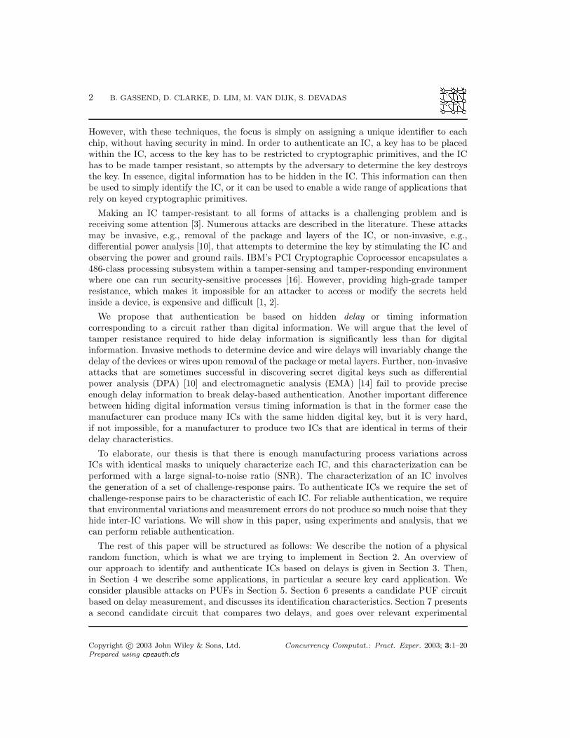
Figure 1. The switch component. For bi = 0 the paths go straight through, for bi = 1 the paths arecrossed.
6. The MAX Circuit
Finding a delay circuit that produces a satisfactory PUF that is provably hard to break isdifficult because of the numerous different types of attacks that are possible. It is unclear howclassical hard problems such as factorization or discrete logarithm could be embedded in theanalog behavior of a physical system.
This section shows a candidate circuit that we have performed experiments on. Weconjectured in [9] that this circuit would be difficult to break in the additive delay model(see Section 8.1), in which we assume that the delay of a complex circuit can be exactlybroken up into a sum of delays of components that make it up. More recent work on a similarcircuit that we present in Section 7 suggests that our conjecture was incorrect. Therefore,to create a PUF that is secure in the additive delay model, modifications will be needed tomake this circuit more difficult to analyze. For practical purposes, we believe that the sheercomplexity of determining circuit delays precisely enough might turn out to be sufficient toprevent modeling attacks on PUFs. Papers such as [11] show just how difficult precise delaysimulation can be.
The circuit for which we will measure delays that is implemented in our key card is depictedin Figure 2. A challenge of n = 128 bits is transformed by a pseudorandom function into abit pattern b = (b1, . . . , bn). The bits bi control switches. If bi = 0, the switch is uncrossed(Figure 1(a)); if bi = 1, the switch is crossed (Figure 1(b)). To get a response from thiscircuit, we present a rising edge on its input. That edge is split into two competing edgesthat independently propagate through the switches until they reach the AND gate. When theslowest of the two edges reaches the AND gate, an edge appears on the output of the circuit.The response of the circuit is the time it took for the edge on the input to produce an edgeon the output.
In the additive delay model, this response of the circuit for a given challenge can be expressedas the max of two sums of elementary path delays. Thus we clearly see the need for the ANDgate. Without it, responses would be linear combinations of elementary delays, and obtainingelementary delays from challenge-response pairs would reduce to solving a linear system ofequations. With the AND gate, each challenge-response pair produces two candidate equations,
Copyright c© 2003 John Wiley & Sons, Ltd. Concurrency Computat.: Pract. Exper. 2003; 3:1–20Prepared using cpeauth.cls

IDENTIFICATION AND AUTHENTICATION OF INTEGRATED CIRCUITS 9
b3b2b1 b128b127
Pseudorandom Functionchallenge
. . .
switch
AND
Figure 2. The proposed MAX circuit
only one of which actually holds. Ideally for k pairs, the adversary would have 2k differentsystems of equations to choose from, though we expect an intelligent adversary to be able toeliminate many of these possibilities.
If the adversary is able to directly chose the bi that gets presented to the device then thereare easy ways for him reduce the number of systems of equations he must deal with. Forexample, by choosing two sets of bi that only differ on two neighboring terms, there is a highlikelihood that the same path was the slowest in both cases, in this way only two of the fourpossible systems of equations need to be considered. With a little more work, the individualdelays in the circuit can once again be found by solving a linear system of equations. Toprevent this type of attack, we do not allow the adversary to directly chose the bi values. Anerror correcting code would be sufficient to prevent the attack we described. We chose to usea pseudorandom function as it allows us to prevent any kind of chosen challenge attack.
One more precaution is necessary. If one elementary delay is much longer than all the others,then it will always be in the slowest path through the circuit, which once again reduces theadversary’s work to solving a linear system of equations. This problem is particularly seriousif the same elementary delay is particularly long on all instances of the device. To preventthis problem, the delay circuit we request that the circuit be designed to be as symmetricalas possible. That way, knowledge of the circuit layout cannot help the adversary guess whichpath through the circuit is the slowest. Moreover, with these precautions, the likelihood thatone elementary delay will be much longer than the others through random process variationsis kept to a minimum.
Copyright c© 2003 John Wiley & Sons, Ltd. Concurrency Computat.: Pract. Exper. 2003; 3:1–20Prepared using cpeauth.cls

10 B. GASSEND, D. CLARKE, D. LIM, M. VAN DIJK, S. DEVADAS
6.1. Circuit details
In order to prove that identification is possible using delay variations between IntegratedCircuits, we have implemented a PUF on Xilinx Spartan 2 FPGAs.§ In these tests, identicalcircuits were placed on different FPGAs, and the resulting PUFs were compared. Our goal inthis section is to show that the identification is possible given the measurement noise levelsand manufacturing variations that we have observed.
Because we do not have full control over the circuits that are implemented in an FPGA, afew compromises have to be made relative to the theoretical design.
First, the unpredictability of the MAX-circuit relies on having a circuit with a high levelof symmetry between paths. The general purpose routing infrastructure of an FPGA makesit difficult to produce precisely matched paths. Therefore the FPGA circuits that we workedwith do not have the degree of symmetry that would be required for a PUF to be secure.However, since the asymmetry is the same across all components, it does not make any changeto the difficulty in identifying components, which is what we will be discussing in this section.
The second limitation of FPGAs, is that the lack of analog components makes it impracticalto directly measure the delay of a path through the circuit with the precision that we require.To get around this problem, we use self-oscillating loops containing the path for which wewant to measure the delay. Using digital circuitry, we can precisely measure the frequency ofthe self oscillating loops over a few tens of thousands of periods.
Note, however, that the use of self oscillating loops to measure delays is not ideal, and shouldnot be used for a production design. First it drastically increases the time (and power) that isrequired to evaluate the PUF. Worse, it makes the frequency that is being measured, which isthe response of the PUF to a challenge, vulnerable to differential power analysis. This is notvery problematic for a key card application, but can be fatal in the case of Controlled PUFs(see [7]).
Figure 3 shows how a self oscillating loop is built around the delay circuit. Since this self-oscillating loop has to be used both for rising and falling transitions, the and gate that combinesthe two paths of the delay circuit of Figure 2 has been replaced by a more complicated circuitthat switches when the slowest transition, be it rising or falling, reaches it. The circuit isessentially a flip-flop that changes state when both outputs from the delay circuit are at thesame level.
The dotted box indicates a delicate part of the circuit that cannot be implemented exactlyas shown without running the risk of producing glitching in the output. In the FPGA itis implemented by a lookup table. In an implementation with simple logic, it should beimplemented in normal disjunctive form. The representation that was used here was simplychosen for ease of understanding.
§The exact components that were used were the XC2S200PQ208-5.
Copyright c© 2003 John Wiley & Sons, Ltd. Concurrency Computat.: Pract. Exper. 2003; 3:1–20Prepared using cpeauth.cls

IDENTIFICATION AND AUTHENTICATION OF INTEGRATED CIRCUITS 11
...
...
Figure 3. Measuring delays using self-oscillating loops
6.2. Robustness to Environmental Variation
So far, all our discussion has considered that path delays in a circuit are constant for a givencomponent. In reality, this is far from the case. Environmental perturbations can account forvariations that are large enough to mask out the small manufacturing variations that we aretrying to measure. Therefore, they must be taken into account.
6.2.1. Temperature and Voltage Compensation
Parameters such as temperature or supply voltage can cause variations in delay that are ordersof magnitude greater than the manufacturing variations that we are trying to observe. For a30 degree Celsius change in temperature, the delays vary on the order of 5%. This is to becompared with inter-chip variations that are well below 1% on this size of circuit.
Fortunately, we have found that environmental variations operate roughly proportionally onall the delays in our circuit, and therefore, they can be compensated for by always workingwith delay ratios instead of absolute delays. Therefore, we place two different self-oscillatingloops on the FPGA. We run both self-oscillating loops to get two frequencies, and take a ratioof the two frequencies as the PUF’s response.
Once compensation has been applied, the variation with temperature is of the same orderof magnitude as the measurement error.
For very large temperature changes (at least greater than 30 degrees Celsius), we can nolonger expect to reliably recognize a PUF. The answer to this problem is to characterize thePUF once when it is hot and once when it is cold (more steps are possible for large temperatureranges). During use, one of these two cases will apply, so the PUF will be correctly recognized.
Up to now, we have assumed that temperature is uniform across the integrated circuit. Ifthat is not the case then temperature compensation is likely not to work well. With the circuitpresented here, the paths are heated in a uniform way by the transitions that are runningthrough them. With other circuits in which transitions only reach some parts of the circuit, we
Copyright c© 2003 John Wiley & Sons, Ltd. Concurrency Computat.: Pract. Exper. 2003; 3:1–20Prepared using cpeauth.cls
12 B. GASSEND, D. CLARKE, D. LIM, M. VAN DIJK, S. DEVADAS
0.96 0.97 0.98 0.99 1 1.01 1.02 1.03
prob
abili
ty d
ensi
ty
compensated measurement
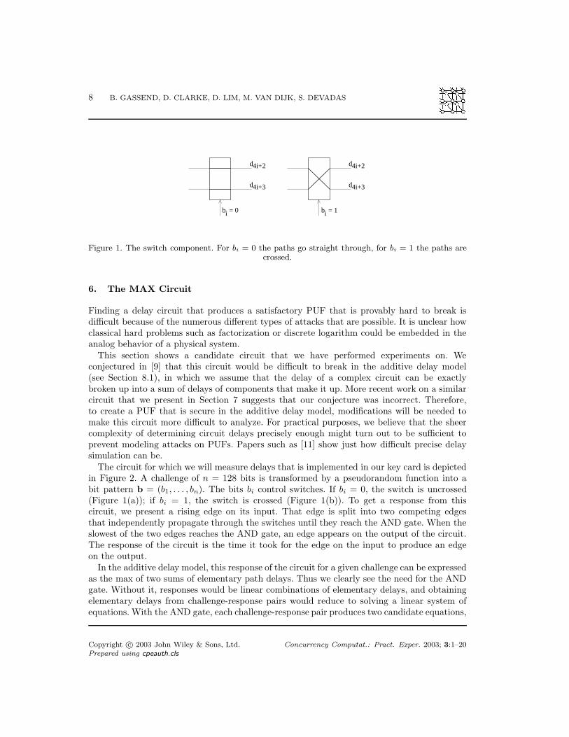
Figure 4. Distribution of responses to randomly selected challenges. Each response is the ratio of thefrequencies of two simultaneously-running loops. As can be seen, when the loop frequencies are too
close, the loops lock and the response is unity.
have observed non uniform heating which can cause unreliable measurement results. Therefore,we recommend the use of circuits that get heated in a uniform way during use.
6.2.2. Interference With Other Sub-Systems
Another kind of environmental interference that has to be considered is the interaction betweena self-oscillating loop, and other circuitry on the integrated circuit.
Experiments in which we measure the frequency of a loop oscillating alone, or at the sametime as other loops show that the interference is very small. This has been demonstrated in[8] where the interference was provided by seven self-oscillating loops, and once again in ourlatest experiments where the frequencies of the two loops that are being measured can bemeasured simultaneously or successively. In each case, the interference caused by the otherself-oscillating loops is of the same order of magnitude as measurement error.
There is however one case in which interference is non negligible. It is the case when theinterference is at almost the same frequency as the self-oscillating loop. In that case, the loop’sfrequency tends to lock on the perturbating frequency. Because of this, it is recommendednot to simultaneously measure the two frequencies that will get combined into a compensatedmeasurement. Figure 4 shows the result of locking on compensated measurements: values nearunity have been forced towards unity by the locking phenomenon.
6.2.3. Aging
Through prolonged use, the delays of an integrated circuit are known to shift. We have notyet studied the effect that aging might have on a PUF. In particular, if the changes due to
Copyright c© 2003 John Wiley & Sons, Ltd. Concurrency Computat.: Pract. Exper. 2003; 3:1–20Prepared using cpeauth.cls
IDENTIFICATION AND AUTHENTICATION OF INTEGRATED CIRCUITS 13
0
0.1
0.2
0.3
0.4
0.5
0.6
0.7
0.8
0.9
1
1e-06 1e-05 0.0001 0.001 0.01
Abe vs. Hal
Abe vs. Abe, same conditions
Abe vs. Abe 10 deg. Celsius hotter
Abe vs. Walt
Abe vs. Abe, different test boards
Abe vs. Abe 20 deg. Celsius hotterAbe vs. Abe 30 deg. Celsius hotter
Figure 5. Comparing the FPGA called Abe at room temperature with itself in various conditions, orwith other FPGAs. The vertical axis indicates the probability that for a given challenge, the differencein response will be lower than the difference in response that is indicated on the horizontal axis. These
plots illustrate the typical behavior we encountered in our experiments with many FPGAs.
aging are big enough, we might not be able to recognize a PUF after it has undergone muchuse. Studying these aging effects is an important aspect that must be covered by future work.
6.3. Identification Abilities
To test our ability to distinguish between FPGAs, we generated a number of profiles for manydifferent FPGAs in different conditions. A profile is made up of 128 challenge-response pairs.All the profiles were established using the same challenges.
Two profiles can be compared in the following way: For each challenge look at the differencebetween the responses. You can then look at the distribution of these differences. If most ofthem are near zero, then the profiles are close. If they are far from zero then the profiles aredistant. During our experiments, the distribution of differences was typically Gaussian, whichallows us to characterize the difference between two profiles by a standard deviation.
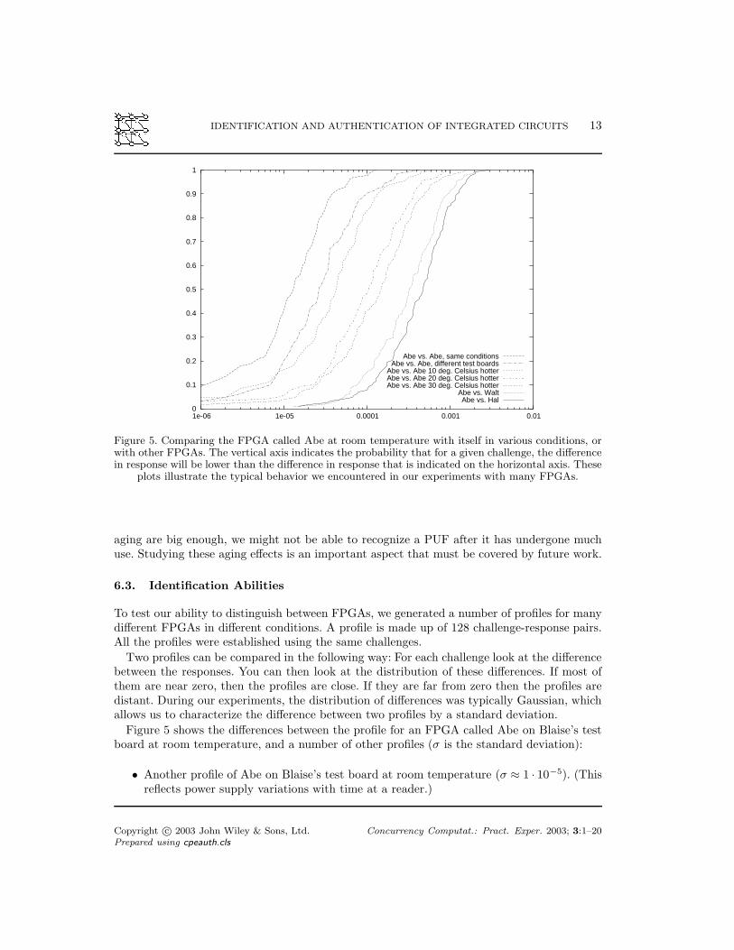
Figure 5 shows the differences between the profile for an FPGA called Abe on Blaise’s testboard at room temperature, and a number of other profiles (σ is the standard deviation):
• Another profile of Abe on Blaise’s test board at room temperature (σ ≈ 1 · 10−5). (Thisreflects power supply variations with time at a reader.)
Copyright c© 2003 John Wiley & Sons, Ltd. Concurrency Computat.: Pract. Exper. 2003; 3:1–20Prepared using cpeauth.cls

14 B. GASSEND, D. CLARKE, D. LIM, M. VAN DIJK, S. DEVADAS
• A profile of Abe on Tara’s test board at room temperature (σ ≈ 2.5 ·10−5). (This reflectspower supply variations across card readers.)
• Profiles of Abe on Blaise’s test board at 10, 20 and 30 degrees Celsius above roomtemperature (σ ≈ 5 · 10−5 to 1.5 · 10−4).
• Profiles of FPGAs Hal and Walt on Blaise’s test board at room temperature (σ ≈ 4·10−4).
The above standard deviations were typical across different FPGAs and comparisons ofdifferent pairs of FPGAs.
Clearly, it is possible to tell FPGAs apart. Though our ability to tell them apart dependson how much environmental variation we need to be robust to. Even with 30 degree Celsiusvariations, each challenge is capable of providing 0.7 bits of information about the identity ofthe FPGA. This goes up to 1.5 bits if only 10 degree Celsius variations are allowed.
If we want to distinguish between 1 billion different components we need a sufficient numberof bits to identify 1018 ≈ 260 components (this is because of the birthday phenomenon). Gettingthose 60 bits of information requires from 40 to 90 challenges depending on the temperaturevariations that we are willing to tolerate.
The numbers that are given here are very dependent on the PUF circuit that is considered.In the circuit that we studied in [8] we had a signal to noise ratio that was much better than weobserved in the current circuit. We believe that by paying more attention to how our circuitis laid out, we will be able to build PUFs for which more bits can be extracted from eachchallenge.
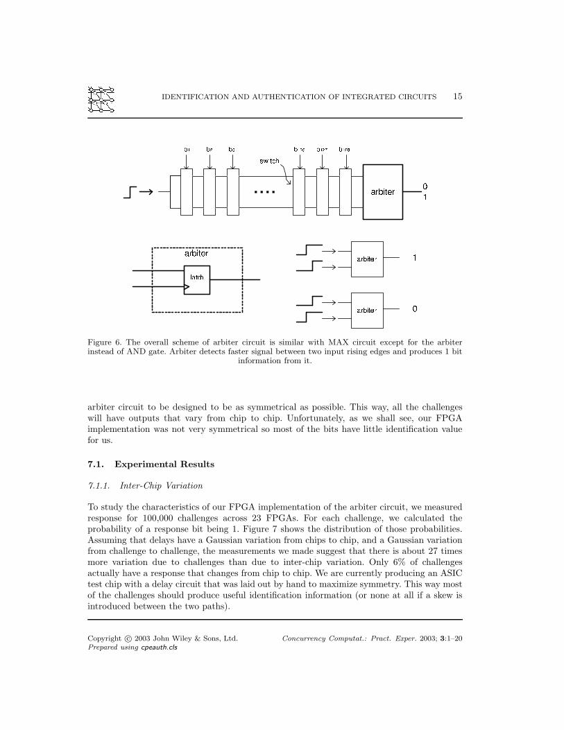
7. The Arbiter Circuit
Measuring delays using self-oscillating circuits as we did in Section 6 is easy and precise.However, to get a precision in the hundreds of parts per million requires tens to hundreds ofthousands of clock cycles, which implies that thousands of edges will have to be propagatedthrough the delay circuit each time we want to measure a single delay. This means thatmeasurement is slow. To make delay measurement faster, we are trying to do direct delaymeasurements, which only run a single edge through the delay circuit. This is not a trivialtask given that in our experiments, we have to measure the delays with precisions on the orderof tens of picoseconds.
The method that we have chosen to explore is to use an arbiter. The arbiter has two inputs,which are both low initially. The arbiter waits for one of the inputs to go high, at which timeits output indicates which input went high first.
Figure 6 shows the structure of arbiter circuit and its operation. We are assuming as forthe MAX circuit that the challenge has been through a pseudorandom function before beingfed into the delay circuit. Two signals race through the delay paths that are defined by thechallenge input bits. At the end of circuit, the arbiter decides which signal arrived first andoutputs a bit.
If the difference in delay for the two racing paths isn’t much larger than the inter-chipvariation in delay, then the value of the output bit is likely to be different from one chip toanother, which makes identification possible. For this reason, it is highly desirable for the
Copyright c© 2003 John Wiley & Sons, Ltd. Concurrency Computat.: Pract. Exper. 2003; 3:1–20Prepared using cpeauth.cls
IDENTIFICATION AND AUTHENTICATION OF INTEGRATED CIRCUITS 15
Figure 6. The overall scheme of arbiter circuit is similar with MAX circuit except for the arbiterinstead of AND gate. Arbiter detects faster signal between two input rising edges and produces 1 bit
information from it.
arbiter circuit to be designed to be as symmetrical as possible. This way, all the challengeswill have outputs that vary from chip to chip. Unfortunately, as we shall see, our FPGAimplementation was not very symmetrical so most of the bits have little identification valuefor us.
7.1. Experimental Results
7.1.1. Inter-Chip Variation
To study the characteristics of our FPGA implementation of the arbiter circuit, we measuredresponse for 100,000 challenges across 23 FPGAs. For each challenge, we calculated theprobability of a response bit being 1. Figure 7 shows the distribution of those probabilities.Assuming that delays have a Gaussian variation from chips to chip, and a Gaussian variationfrom challenge to challenge, the measurements we made suggest that there is about 27 timesmore variation due to challenges than due to inter-chip variation. Only 6% of challengesactually have a response that changes from chip to chip. We are currently producing an ASICtest chip with a delay circuit that was laid out by hand to maximize symmetry. This way mostof the challenges should produce useful identification information (or none at all if a skew isintroduced between the two paths).
Copyright c© 2003 John Wiley & Sons, Ltd. Concurrency Computat.: Pract. Exper. 2003; 3:1–20Prepared using cpeauth.cls

16 B. GASSEND, D. CLARKE, D. LIM, M. VAN DIJK, S. DEVADAS
0
0.05
0.1
0.15
0.2
0.25
0.3
0.35
0.4
0.45
0.5
0 0.2 0.4 0.6 0.8 1
Pro
babi
lity
Den
sity
Pr(response = 1)
P(Pr(response=1)=0) = 0.56
P(Pr(response=1)=1) = 0.38
Figure 7. How much the output of a challenge varies from chip to chip. The sample space is the set ofchallenges. Triangles show experimental data, the line shows an fit with a theoretical model. For our
circuit the vast majority of challenges had the same output on all the chips we measured.
To study how different chips are from each other, we look at the number of challenges in our100,000 challenge test set that change from one chip to another; this is called the Hammingdistance. In our experiments with 23 FPGAs, the average Hamming distance between chipswas 1049, roughly 1.05% of the challenges.
7.1.2. Measurement Noise
To evaluate measurement noise, we measured a set of 10,000 (FIXME) challenges 23 (FIXME)times each. Challenges that didn’t return the same value each time were counted as unreliable.In this way, we found that about 0.098% of challenges were unreliable on the PUF arbitercircuit. Since this is more than ten times less than the distance between two distinctcomponents, identifying chips using this circuit is easy.
When considering this number, one should keep in mind that the challenges that areunreliable are most likely the ones that have comparable delays for both of the racing paths, i.e.,precisely the ones that are useful for identification purposes. Therefore, in a more symmetricalcircuit, the number of useful challenges for identification will increase hand in hand with themeasurement noise.
Copyright c© 2003 John Wiley & Sons, Ltd. Concurrency Computat.: Pract. Exper. 2003; 3:1–20Prepared using cpeauth.cls

IDENTIFICATION AND AUTHENTICATION OF INTEGRATED CIRCUITS 17
0
0.2
0.4
0.6
0.8
1
1.2
1.4
0 5 10 15 20 25 30 35 40
Noi
se %
(N)
Temperature difference(celsius)
Best Model Limit (0.61%)
Inter FPGA Variation (1.049%)
Measurement noise (0.098%)
Temp variation
Figure 8. Variation in normalized Hamming distance (noise) when a chip is compared with itself ata different temperature. For comparison the inter-chip variation and our best attempt at a model-
building attack are also shown.
7.1.3. Temperature variation
A nice aspect of the arbiter circuit is that since it is comparing the delays of two paths throughthe circuit, it is automatically applying the temperature compensation methods that we hadto explicitly introduce for circuits that were based on delay measurements.
Figure 8 shows the amount of noise introduced by temperature variation. We made a profilefor 100,000 challenges at the reference temperature of 28 degrees Celsius and calculated itsdistance from the response vector at increasingly higher temperatures. Even with a changein temperature greater than 40 degrees Celsius, the noise is only about 0.3%, well below theinter-chip variation of 1.06%
Overall, the arbiter circuit has qualitatively comparable performance to the delaymeasurement circuit. If the proportion of challenges that are useful for identification can beincreased, it will be much faster to use than the delay measurement circuit, which makes it anexcellent candidate for PUF applications.
Copyright c© 2003 John Wiley & Sons, Ltd. Concurrency Computat.: Pract. Exper. 2003; 3:1–20Prepared using cpeauth.cls

18 B. GASSEND, D. CLARKE, D. LIM, M. VAN DIJK, S. DEVADAS
8. Modeling Attacks
As we have seen in Section 5.2, it must be difficult for on attacker to build an accurate timingmodel of our circuit if we want to prevent him from impersonate it. To evaluate the difficultyof this type of attack we tried to carry it out ourselves. The results we have to date suggestthat the basic MAX and arbiter circuits are not difficult enough to model, contrarily to whatwe had conjectured in [9].
8.1. Additive-Delay Model
We model the circuits in the additive model. In this model, we assume that the delay of apath through the circuit is the sum of the delays of the elementary components that makeup the circuit. Knowing all the elementary component delays an attacker can calculate thecircuit delay for any challenge. The attacker’s task is to find the elementary delays. Assumingthat getting the elementary delays by opening the circuit and doing direct measurement isimpractical, we see that an attacker will have to infer those delays from the outputs of thedevice on a number of challenges. Because of the pseudorandom function that has been placedin the circuit, the challenges that the adversary has to work with are effectively random.
The circuits we have considered in sections 6 and 7 are made up of a sequence of identicalstages, each containing a switch block. The switch block can be modeled by using 4 delaysas shown in Figure 9(a). But this representation contains a lot of redundancy. First, as isshown in Figure 9(b), the delay can be separated into a symmetric and an antisymmetricpart. The symmetric part gets added to both paths, and the antisymmetric part added toone path and subtracted from the other. Finally, we note that the point where one stagestarts and the next one ends isn’t clearly defined. By moving those points around, the numberof parameters to describe a stage can be reduced to 2 as illustrated in Figure 9(c). One todescribe the difference that the challenge bit makes to the symmetric part, and one to describethe difference in delay between the two paths between the two paths. Repeating this operationat each stage, and reordering the symmetric part leads to simplified circuit in Figure 9(d). Alltogether the n switched stages are modeled by using 2n+2 parameters. For the arbiter half ofthose parameters are unnecessary as only the difference between the two delays is consideredby the arbiter.
Algebraically, the delay of the top path can be expressed as
n∑
i=0
(−1)civi + v∗ +
n∑
i=0
(−1)piyi + y∗
where pi = ci ⊕ · · · ⊕ cn and ⊕ denotes the exclusive-or operation. The delay of the bottompath is similar except that all the y terms have a change of sign. As we can see, the delay canbe seen as the sum of a constant and two dot products of delays by a vector that is a functionof the challenge. In the arbiter case there is only one dot product as the symmetric part is ofno use.
Copyright c© 2003 John Wiley & Sons, Ltd. Concurrency Computat.: Pract. Exper. 2003; 3:1–20Prepared using cpeauth.cls

IDENTIFICATION AND AUTHENTICATION OF INTEGRATED CIRCUITS 19
a
b
c
d
a’
c’
d’
b’
(a)
c’
d’
b’
a’(a+b)/2
(a+b)/2
(c+d)/2
(c+d)/2
(a−b)/2
(b−a)/2
(d−c)/
2
(c−d)/2
(b)
a’+x+u
b’−x+u
d’−x+
u
c’+x+u
u=(a+b+c+d)/4
y=(a−b+c−d)/4x=(a−b−c+d)/4v=(a+b−c−d)/4
y
−y0
0
0
0
v
−v
v
−v
(c)
c0
vn
cnc0
v0
−v0
...*v
−vn
cn
y*0
0
y
...
... yn
n−y −y *−y
(d)
Figure 9. Simplifying the delay model of a switch block and resulting simplified model of a switch-baseddelay circuit. The dots represent the points between which delays are measured.
Copyright c© 2003 John Wiley & Sons, Ltd. Concurrency Computat.: Pract. Exper. 2003; 3:1–20Prepared using cpeauth.cls
20 B. GASSEND, D. CLARKE, D. LIM, M. VAN DIJK, S. DEVADAS
8.2. The Perceptron Algorithm
The perceptron algorithm [17] is the simplest available algorithm for training single layeredneural networks. In such a network, the output of a neuron is computed by taking the dotproduct of an input vector (typically a vector of +1 and -1) with a vector of weights, andcomparing the result with a threshold. To train such a neuron on a set of input vectors, onesimply iterates through the input vectors. If an input produces the correct output, nothing ischanged. If an input produces an incorrect result, each one of the neuron’s weights in changedin the direction that would tend to make it produce the correct result.
If the training set can be learned by the neural network (i.e., if the two types of outputs canbe separated by a hyper-plane in the input space), then the perceptron algorithm convergesto a solution that satisfies all the training cases. If not, a slightly improved version of thealgorithm can be used, which converges to the set of weights that maximizes the number oftraining cases that the neuron correctly decides.
According to the analysis we did in Section 8.1 the arbiter circuit can be viewed as a neuron,where the weights are a function of the elementary circuit delays, and the input vector is asimple function of the challenge bits. Therefore, we can expect the arbiter circuit to be veryeasy to build a model for under the additive delay model. What remains to be seen is whetherthe additive delay model is precise enough to produce a model that can be used to impersonatea physical device.
Because of the MAX operation, and because it has a real valued output, the MAX circuitcannot be reduced exactly to the perceptron algorithm, however, we found that a slightlymodified algorithm gives excellent results. The method is as follows: first the model is initializedwith random elementary delays. Then for each example in the training set, the output of thecircuit is calculated. Based on how far the output is from the desired output, the elementarydelays on the path that was selected by the MAX function are adjusted to bring the outputcloser to the desired value. In numerical experiments, we found that this method usuallyperfectly learned the training set (in rare cases it gets stuck far from the correct solution, butslightly different starting parameters then lead to perfect convergence). When noise was addedto the experiments, the algorithm converged to within the amount of noise that was added.
At this point, we must conclude that if the additive delay model applies sufficiently preciselyto our circuits, then a model building attack is possible and even easy. This does not necessarilymean that the real circuits can be modeled though, as the additive delay model is not preciseenough to properly model the real device.
8.3. Modeling Experiments
To try to get an idea of how much our circuit deviates from the additive delay model, weattempted to train a model of the arbiter circuit using 90,000 challenge-response pairs measuredon our FPGA implementation. When evaluated on a different set of 100,000 challenge-responsepairs, the success rate of the model was only about 96.7%. This is greater than the inter-chipvariation, so one would be better off using a different FPGA than using our model whenattempting to impersonate a chip.
Copyright c© 2003 John Wiley & Sons, Ltd. Concurrency Computat.: Pract. Exper. 2003; 3:1–20Prepared using cpeauth.cls

IDENTIFICATION AND AUTHENTICATION OF INTEGRATED CIRCUITS 21
?
?
?
?
?
?
?
?
A
B
A
B
C
O
?
?
?
?
?
?
?
?
A rising, B = 0, C = 0 A rising, B = 1, C = 0
11
1
1 0
0
0
0
C
C = 1C = 0 Unused
A = 0, B = 0
A = 1, B = 1
A = 0, B = 1
A = 1, B = 0
O
11
1
1 0
0
0
0
0
A
B
C
C = 1C = 0 Unused
A = 0, B = 0
A = 1, B = 1
A = 0, B = 1
A = 1, B = 0
O
MultiplexerMultiplexer
Decode
Decode
0
Figure 10. In a lookup table implementation of a multiplexer, the path that is taking by a rising edgeon input A to get to output O depends on the state of input B.
Our initial hypothesis for these disappointing (from the attacker’s point of view) results wasthat we were getting interference between the two paths through the delay circuit. Indeed, theswitch component in the delay path is implemented by using a pair of multiplexer (MUX), thateach have the challenge bit and both of delay paths as inputs. In Xilinx FPGAs, combinationallogic is mainly implemented using 4 input look up tables (LUT). In particular, in the circuitwe implemented, the MUXes were being implemented as LUTs. These LUTs are laid out as4 by 4 grids of SRAM cells as shown in Figure 10. As the figure shows, a rising edge thatgoes through the MUX takes a different path through the grid depending on the value ofthe spectator input that is not currently selected. To take this difference into account wouldrequire a more complex model than the one we had considered.
To verify this hypothesis, we resynthesized our circuit using the MUXCY component thatis part of the FPGA’s fast carry logic, hoping that this component would be implemented insuch a way that the path through the multiplexer does not depend on the spectator input.This was a reasonable assumption as most multiplexer implementations have this property.This time, the perceptron algorithm gave us a model that had a success rate of 99.4%. This isstill above measurement noise, even with 40 degree Celsius variations in temperature, but iswell below inter-chip variation (see Figure 8).
At this point, we cannot say that the arbiter circuit of Figure 6 is broken, but an extremelysimple modeling effort has been able to get uncomfortably close to measurement noise forone implementation of the arbiter circuit. Similar experiments are currently underway for theMAX circuit.
Copyright c© 2003 John Wiley & Sons, Ltd. Concurrency Computat.: Pract. Exper. 2003; 3:1–20Prepared using cpeauth.cls

22 B. GASSEND, D. CLARKE, D. LIM, M. VAN DIJK, S. DEVADAS
arbiter
b127 b128
. . .
switch
output
challenge
(ignored)
. . .
bb100 101
Figure 11. Adding unknown challenge bits using a feed-forward arbiter
OutputInput
Control
OutputInput
Control
(a) Two implementations
bb
Switch Switch . . .. . .
i i+1
(b) In a circuit
Figure 12. Variable-delay buffers
8.4. Hardening the Circuit
Our experimental results suggest that the circuits we have proposed to date are not as strongagainst modeling attacks as we would like. A number of directions can be taken to try to makethe circuit stronger, evaluating these options will be the object of future work.
Feed forward arbiter: An arbiter is placed at an intermediate point in the circuit, its outputdrives one of switches later on in the circuit (Figure 11). Many such arbiters could beadded to the circuit for increased difficulty. The major problem with this approach isthat it adds discontinuities in the circuit, i.e., conditions in which a slight change in adelay (due to noise, for example) can lead to a huge difference in the delay of a path.Moreover, this circuit can easily be expressed in the additive delay model, and we fearthat a variant of the perceptron algorithm would be able to break it.
Copyright c© 2003 John Wiley & Sons, Ltd. Concurrency Computat.: Pract. Exper. 2003; 3:1–20Prepared using cpeauth.cls

IDENTIFICATION AND AUTHENTICATION OF INTEGRATED CIRCUITS 23
Variable delay buffers: Here we try to add interactions between the paths through thecircuit, as was the case with the lookup-table multiplexer implementation. This is doneby using what we call a variable delay buffer (see Figure 12). A component that directlypasses a signal from its input to its output, but that does so at a different speed dependingon the state of its other input. This approach is nice as it leads to continuous but non-monotonic circuits (the delay of the circuit is a continuous function of the elementarycircuit delays, but the total delay might decrease as the delay of an elementary delayincreases). Moreover, by putting some effort into the delay characteristics of the variabledelay buffer, the circuit can be made hard to model in the additive delay model.
Change the circuit topology: So far we have only explored an extremely simple circuittopology, there are scores of other possibilities left to explore. The three things to aimfor are reliability, variability and modeling difficulty. To achieve reliability one majorcriterion is that the total circuit delay should vary slowly with the elementary componentdelays. For variability (two chips with different delays have different responses), that samevariation should not be too slow. The hardest part is modeling difficulty; for now it isessentially an open problem.
9. Conclusion
In this paper we have presented a technique for delay-based circuit authentication andconducted preliminary experiments that show that it is viable. By using this method, it ispossible to store secrets on a chip in a way that is less vulnerable to invasive attacks thantraditional digital methods.
Experimental results have shown that there is enough variations between integrated circuitsfor identification purposes, and that the effect of temperature and power supply voltagevariations can be mitigated, allowing robust identification. More experiments are necessaryunderstand the effects of circuit aging on identification ability.
We have argued that delay-based authentication is not susceptible to conventional attacksthat attempt to discover a secret, hidden key. The most plausible attack we have foundagainst our devices is the model-building attack. Our experiments suggest that the currentimplementation of our devices could be vulnerable to this type of attack, but we have suggesteda number of mechanisms that might prevent these attacks.
While a number of problems need to be solved in order to use delay-based authenticationin applications such as smart card authentication and software licensing, we believe that thisis a promising direction for future research.
REFERENCES
1. R. Anderson and M. Kuhn. Tamper Resistance - a Cautionary Note. In Proceedings of the Second UsenixWorkshop on Electronic Commerce, pages 1–11, Nov. 1996.
2. R. Anderson and M. Kuhn. Low Cost Attacks on Tamper Resistant Devices. In IWSP: InternationalWorkshop on Security Protocols, LNCS, 1997.
Copyright c© 2003 John Wiley & Sons, Ltd. Concurrency Computat.: Pract. Exper. 2003; 3:1–20Prepared using cpeauth.cls

24 B. GASSEND, D. CLARKE, D. LIM, M. VAN DIJK, S. DEVADAS
3. R. J. Anderson. Security Engineering: A Guide to Building Dependable Distributed Systems. John Wileyand Sons, 2001.
4. D. S. Boning and S. Nassif. Models of Process Variations in Device and Interconnect. In W. B.A. Chandrakasan and F. Fox, editors, Design of High Performance Microprocessor Circuits, chapter 6.IEEE Press, 2000.
5. D. Chinnery and K. Keutzer. Closing the Gap Between ASIC & Custom. Kulwer Academic Publishers,2002.
6. F. Dartu and L. T. Pileggi. Calculating worst-case gate delays due to dominant capacitance coupling. InProceedings of the 34th annual conference on Design automation conference, pages 46–51. ACM Press,1997.
7. B. Gassend, D. Clarke, M. van Dijk, and S. Devadas. Controlled physical random functions. In Proceedingsof 18th Annual Computer Security Applications Conference, December 2002.
8. B. Gassend, D. Clarke, M. van Dijk, and S. Devadas. Silicon physical unknown functions. Technicalreport, MIT LCS TR-833, May 2002.
9. B. Gassend, D. Clarke, M. van Dijk, and S. Devadas. Delay-based circuit authentication and applications.In Proceedings of the 2003 ACM Symposium on Applied Computing, March 2003.
10. P. Kocher, J. Jaffe, and B. Jun. Differential Power Analysis. Lecture Notes in Computer Science,1666:388–397, 1999.
11. Y. Liu, S. R. Nassif, L. T. Pileggi, and A. J. Strojwas. Impact of interconnect variations on clock skew ofa gigahertz microprocessor. In Design Automation Conference. IEEE/ACM, June 2000.
12. K. Lofstrom, W. R. Daasch, and D. Taylor. IC Identification Circuit Using Device Mismatch. InProceedings of ISSCC 2000, pages 372–373, February 2000.
13. A. J. Menezes, P. C. van Oorschot, and S. A. Vanstone. Handbook of Applied Cryptography. CRC Press,1996.
14. J.-J. Quisquater and D. Samyde. ElectroMagnetic Analysis (EMA): Measures and Counter-Measures forSmart Cards. In Proceedings of Smart Card Programming and Security (E-smart 2001), LNCS 2140,pages 200–210, September 2001.
15. P. S. Ravikanth. Physical One-Way Functions. PhD thesis, Massachusetts Institute of Technology, 2001.16. S. W. Smith and S. H. Weingart. Building a High-Performance, Programmable Secure Coprocessor. In
Computer Networks (Special Issue on Computer Network Security), volume 31, pages 831–860, April 1999.17. S. Theodoridis and K. Koutroumbas. Pattern Recognition. Academic Press, 2003.18. N. Weste and K. Eshraghian. Principles of CMOS VLSI Design: A Systems Perspective. Addison Wesley,
1985.
Copyright c© 2003 John Wiley & Sons, Ltd. Concurrency Computat.: Pract. Exper. 2003; 3:1–20Prepared using cpeauth.cls