MD-SR60 SERVICE MANUAL - Diagramas dediagramas.diagramasde.com/audio/MDSR6028S29.pdfMD-SR60 CONTENTS...
48
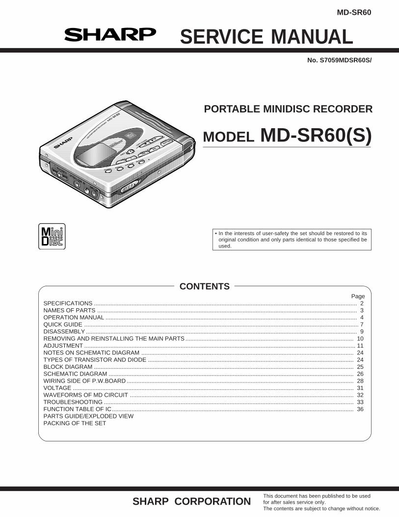
MD-SR60 CONTENTS Page SPECIFICATIONS ................................................................................................................................................................. 2 NAMES OF PARTS ............................................................................................................................................................... 3 OPERATION MANUAL .......................................................................................................................................................... 4 QUICK GUIDE ........................................................................................................................................................................ 7 DISASSEMBLY ...................................................................................................................................................................... 9 REMOVING AND REINSTALLING THE MAIN PARTS ....................................................................................................... 10 ADJUSTMENT ...................................................................................................................................................................... 11 NOTES ON SCHEMATIC DIAGRAM .................................................................................................................................. 24 TYPES OF TRANSISTOR AND DIODE .............................................................................................................................. 24 BLOCK DIAGRAM ............................................................................................................................................................... 25 SCHEMATIC DIAGRAM ...................................................................................................................................................... 26 WIRING SIDE OF P.W.BOARD ........................................................................................................................................... 28 VOLTAGE ............................................................................................................................................................................ 31 WAVEFORMS OF MD CIRCUIT ......................................................................................................................................... 32 TROUBLESHOOTING ......................................................................................................................................................... 33 FUNCTION TABLE OF IC .................................................................................................................................................... 36 PARTS GUIDE/EXPLODED VIEW PACKING OF THE SET SERVICE MANUAL SHARP CORPORATION No. S7059MDSR60S/ This document has been published to be used for after sales service only. The contents are subject to change without notice. MODEL MD-SR60(S) • In the interests of user-safety the set should be restored to its original condition and only parts identical to those specified be used. PORTABLE MINIDISC RECORDER
Transcript of MD-SR60 SERVICE MANUAL - Diagramas dediagramas.diagramasde.com/audio/MDSR6028S29.pdfMD-SR60 CONTENTS...
MD-SR60
CONTENTSPage
SPECIFICATIONS ................................................................................................................................................................. 2NAMES OF PARTS ............................................................................................................................................................... 3OPERATION MANUAL .......................................................................................................................................................... 4QUICK GUIDE ........................................................................................................................................................................ 7DISASSEMBLY ...................................................................................................................................................................... 9REMOVING AND REINSTALLING THE MAIN PARTS ....................................................................................................... 10ADJUSTMENT ...................................................................................................................................................................... 11NOTES ON SCHEMATIC DIAGRAM .................................................................................................................................. 24TYPES OF TRANSISTOR AND DIODE .............................................................................................................................. 24BLOCK DIAGRAM ............................................................................................................................................................... 25SCHEMATIC DIAGRAM ...................................................................................................................................................... 26WIRING SIDE OF P.W.BOARD ........................................................................................................................................... 28VOLTAGE ............................................................................................................................................................................ 31WAVEFORMS OF MD CIRCUIT ......................................................................................................................................... 32TROUBLESHOOTING ......................................................................................................................................................... 33FUNCTION TABLE OF IC.................................................................................................................................................... 36PARTS GUIDE/EXPLODED VIEWPACKING OF THE SET
SERVICE MANUAL
SHARP CORPORATION
No. S7059MDSR60S/
This document has been published to be usedfor after sales service only.The contents are subject to change without notice.
MODEL MD-SR60(S)
• In the interests of user-safety the set should be restored to itsoriginal condition and only parts identical to those specified beused.
PORTABLE MINIDISC RECORDER
MD-SR60
– 2 –
FOR A COMPLETE DESCRIPTION OF THE OPERATION OF THIS UNIT, PLEASE REFER TOTHE OPERATION MANUAL.
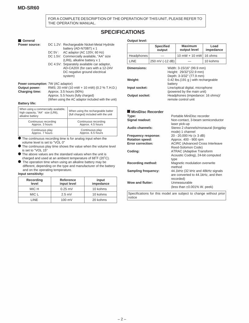
SPECIFICATIONS
Specifications for this model are subject to change without priornotice
Output level:
Dimensions: Width: 3-15/16" (99.9 mm)Height: 29/32"(22.9 mm)Depth: 3-3/32" (77.9 mm)
Weight: 0.42 lbs.(191 g ) with rechargeablebattery
Input socket: Line/optical digital, microphone(powered by the main unit)
Output socket: Headphones (impedance: 16 ohms)/remote control unit
MiniDisc RecorderType: Portable MiniDisc recorderSignal readout: Non-contact, 3-beam semiconductor
laser pick-upAudio channels: Stereo 2 channels/monaural (longplay
mode) 1 channelFrequency response: 20 - 20,000 Hz (± 3 dB)Rotation speed: Approx. 400 - 900 rpmError correction: ACIRC (Advanced Cross Interleave
Reed-Solomon Code)Coding: ATRAC (Adaptive Transform
Acoustic Coding), 24-bit computedtype
Recording method: Magnetic modulation overwritemethod
Sampling frequency: 44.1kHz (32 kHz and 48kHz signalsare converted to 44.1kHz, and thenrecorded)
Wow and flutter: Unmeasurable(less than ±0.001% W. peek)
GeneralPower source: DC 1.2V: Rechargeable Nickel-Metal Hydride
battery (AD-N70BT) x 1DC 5V : AC adaptor (AC 120V, 60 Hz)DC 1.5V: Commercially available, "AA" size
(LR6), alkaline battery x 1DC 4.5V: Separately available car adaptor,
AD-CA20X (for cars with a 12-24VDC negative ground electricalsystem)
Power consumption: 7W (AC adaptor)Output power: RMS; 20 mW (10 mW + 10 mW) (0.2 % T.H.D.)Charging time: Approx. 3.5 hours (90%)
Approx. 5.5 hours (fully charged)(When using the AC adaptor included with the unit)
Battery life:
The continuous recording time is for analog input when thevolume level is set to "VOL 0"The continuous play time shows the value when the volume levelis set to "VOL 15"The above values are the standard values when the unit ischarged and used at an ambient temperature of 68˚F (20˚C).The operation time when using an alkaline battery may bedifferent, depending on the type and manufacturer of the batteryand on the operating temperature.
Input sensitivity:
MIC H 0.25 mV 10 kohms
MIC L 2.5 mV 10 kohms
LINE 100 mV 20 kohms
Recordinglevel
Referenceinput level
inputimpedance
When using a commercially available,high capacity, "AA" size (LR6),alkaline battery
When using the rechargeable batter(full charged) included with the unit
Continuous recordingApprox. 3 hours
Continuous recordingApprox. 4.5 hours
Continuous playApprox. 7 hours
Continuous playApprox. 6.5 hours
Headphones — 10 mW + 10 mW 16 ohms
LINE 250 mV (-12 dB) — 10 kohms
Maximumoutput level
Loadimpedance
Specifiedoutput
MD-SR60
– 3 –
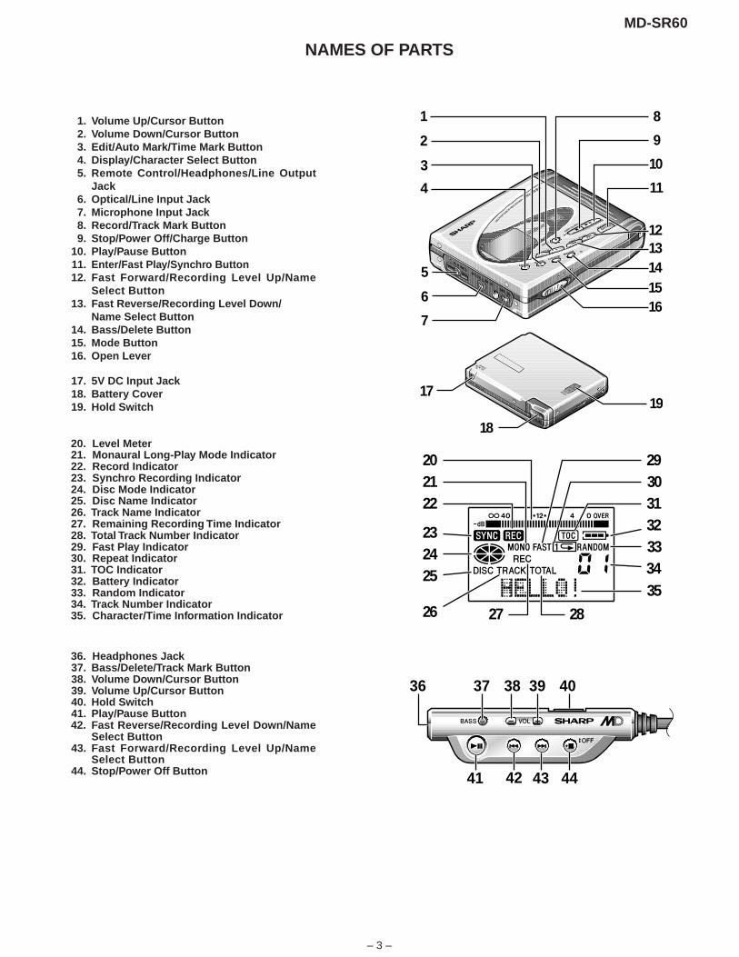
NAMES OF PARTS
1. Volume Up/Cursor Button2. Volume Down/Cursor Button3. Edit/Auto Mark/Time Mark Button4. Display/Character Select Button5. Remote Control/Headphones/Line Output
Jack6. Optical/Line Input Jack7. Microphone Input Jack8. Record/Track Mark Button9. Stop/Power Off/Charge Button
10. Play/Pause Button11. Enter/Fast Play/Synchro Button12. Fast Forward/Recording Level Up/Name
Select Button13. Fast Reverse/Recording Level Down/
Name Select Button14. Bass/Delete Button15. Mode Button16. Open Lever
17. 5V DC Input Jack18. Battery Cover19. Hold Switch
20. Level Meter21. Monaural Long-Play Mode Indicator22. Record Indicator23. Synchro Recording Indicator24. Disc Mode Indicator25. Disc Name Indicator26. Track Name Indicator27. Remaining Recording Time Indicator28. Total Track Number Indicator29. Fast Play Indicator30. Repeat Indicator31. TOC Indicator32. Battery Indicator33. Random Indicator34. Track Number Indicator35. Character/Time Information Indicator
36. Headphones Jack37. Bass/Delete/Track Mark Button38. Volume Down/Cursor Button39. Volume Up/Cursor Button40. Hold Switch41. Play/Pause Button42. Fast Reverse/Recording Level Down/Name
Select Button43. Fast Forward/Recording Level Up/Name
Select Button44. Stop/Power Off Button
4
5
6
7
1312
141516
17
8
10
9
11
2
1
3
18
19
3132333435
2930
202122
232425
26 27 28
36 37 38 39 40
41 42 43 44
MD-SR60
– 4 –
OPERATION MANUAL
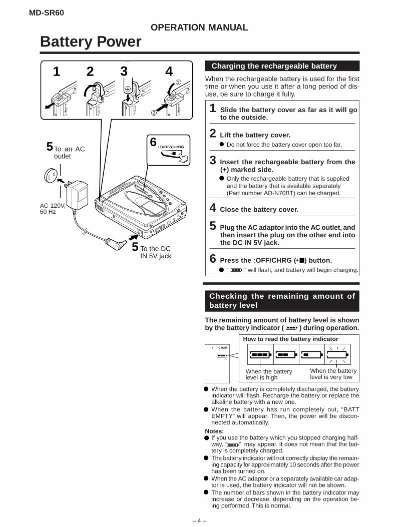
Battery Power
5
1 2 3 41
2
5 6
To the DCIN 5V jack
AC 120V,60 Hz
To an ACoutlet
Charging the rechargeable battery
When the rechargeable battery is used for the firsttime or when you use it after a long period of dis-use, be sure to charge it fully.
1 Slide the battery cover as far as it will goto the outside.
2 Lift the battery cover.Do not force the battery cover open too far.
3 Insert the rechargeable battery from the(+) marked side.
Only the rechargeable battery that is suppliedand the battery that is available separately(Part number AD-N70BT) can be charged.
4 Close the battery cover.
5 Plug the AC adaptor into the AC outlet, andthen insert the plug on the other end intothe DC IN 5V jack.
6 Press the :OFF/CHRG (• ) button.“ ” will flash, and battery will begin charging.
When the batterylevel is high
When the batterylevel is very low
Checking the remaining amount ofbattery level
The remaining amount of battery level is shownby the battery indicator ( ) during operation.
When the battery is completely discharged, the battery indicator will flash. Recharge the battery or replace thealkaline battery with a new one.When the battery has run completely out, “BATTEMPTY” will appear. Then, the power will be discon-nected automatically.
Notes:If you use the battery which you stopped charging half-way, “ ” may appear. It does not mean that the bat-tery is completely charged.The battery indicator will not correctly display the remain-ing capacity for approximately 10 seconds after the powerhas been turned on.When the AC adaptor or a separately available car adap-tor is used, the battery indicator will not be shown.The number of bars shown in the battery indicator mayincrease or decrease, depending on the operation be-ing performed. This is normal.
How to read the battery indicator
MD-SR60
– 5 –
The unit may have the following symptoms while recording or editing. The unit is not malfunctioning.
MiniDisc System Limitations
SYMPTOM
“DISC FULL” or “TOC FULL” appearseven though the MiniDisc still has re-cording time left.
The remaining recording time does notincrease even though you erased tracks.
The total of the recorded time and theremaining time does not match the maxi-mum recordable time.
Combine function does not work.
Sound skips in fast reverse/forward.
A track number is created in the middleof a track.
LIMITATIONS
More than 255 tracks (maximum) cannot be recorded regardless of the re-cording time.If the MiniDisc is recorded or edited repeatedly or if it has scratches (record-ing skips scratched parts), you may not be able to record the maximumtracks above.
The unit does not count non-recorded portions that last 12 or fewer secondsto display the remaining recording time. The time may not increase even ifyou erase short tracks.
One cluster (approximately 2 seconds) is the minimum unit for recording.For example, a 3-second track uses 2 clusters (approximately 4 seconds).Therefore, the actual recordable time may be shorter than the displayedtime.
A MiniDisc on which recording and editing are repeated may not allow thecombine function.
One track is divided and recorded in separate places on a repeatedly re-corded or edited MiniDisc.Sound may skip.
A track number may be created if there are scratches or dust on the MiniDisc.
TroubleshootingMany potential “problems” can be resolved by the owner without calling a service technician.If something seems to be wrong with this product, check the following before calling your authorized SHARP dealer orservice center.
The unit does not turn on.
No sound is heard from the head-phones.
When the operation buttons arepressed, the unit does not respond.
Some sounds are skipped.
The MiniDisc cannot be ejected.
Recording and editing are impossible.
PROBLEM CAUSE
● Is the AC adaptor disconnected?● Is the battery exhausted?● Is the unit in the hold mode?● Has condensation formed inside the unit?● Is the unit being influenced by mechanical shock or by static electricity?
● Is the volume set too low?● Is the remote control unit or the headphones plugged in?● Are you trying to play a MiniDisc with data on it instead of a MiniDisc containing music?
● Is the unit in the hold mode?● Is the battery exhausted?● Is the remote control unit plug or the headphones plug inserted firmly?
● Is the battery exhausted?● Is the unit being subjected to excessive vibration?
● Has the track number or character information been written on the disc yet?● Is the unit in the recording or editing mode?
● Is the MiniDisc protected against accidental erasure?● Is the unit connected properly to the other equipment?● Is the AC adaptor unplugged or did a power failure occur while recording or editing?● Is the unit in the hold mode?● Is an optical signal being output from the stereo system?
Read the operation manual for the stereo system.

MD-SR60
– 6 –
Error MessagesERROR MESSAGES
BATT EMPTY
BLANK MD
Can’t COPY
Can’t EDIT
Can’t READ (*)
Can’t REC
Can’t STAMP
Can’t WRITE
DEFECT
DISC FULL
Er-MD (**)
HOLD
LOCKED
NO DISC
MEANING
● The battery is not charged or thereis no battery in the compartment.
● Nothing is recorded.● You tried to record from a copy pro-
hibited MiniDisc.● A track cannot be edited.
● The disc data cannot be read be-cause the disc is damaged.
● Recording cannot be performed cor-rectly due to vibration or shock.
● Stamp function does not work.
● Cannot save the TOC informationcorrectly to a MiniDisc. (A large por-tion of the disc has been damaged.)
● The disc is scratched.
● The disc is out of recording space.
● The microprocessor has reported asystem fault and the unit is out of or-der.
● The unit is in the hold mode.
● You removed a MiniDisc while re-cording or editing.
● A disc has not been loaded.
Number or symbol appears in (*) position.
REMEDY
● Charge the rechargeable battery or replace the alka-line battery (or use the AC adaptor for power).
● Replace the disc with a recorded disc.● Record using the analog cable.
● Change the stop position of the track and then edit it.
● Reload the disc.● Replace it with another recorded disc.
● Re-record or replace it with another recordable disc.
● Check the number of tracks.
● Replace the disc with another recordable disc.
● If the sound you hear is not right, record again.● Replace the disc with another recordable disc.
● Replace it with another recordable disc.
● To have it repaired, go to the distributor where youpurchased the unit.
● Return the HOLD switch to its original position.
● Turn off the power and remove the MiniDisc.
● Load a disc.
**:80=EEPROM READ ERROR 41=UTOC WRITE ERROR
*:f=focus ERROR r=TOC READ a=SERVO ADJUST u=UTOC READ s=TRACK SEARCH w=Data WRITE
g
ERROR MESSAGES
NO SIGNAL
PLAY MD
POWER ?
PROTECTED
SORRY
TEMP OVER
TOC FORM (**)
TOC FULL
Tr. Protect
? DISC
MEANING
● Poor connection of the digital cable.● No output signal comes out from the
connected unit to playback.
● You recorded on a playback-onlydisc.
● Improper power is being supplied.
● The write protection tab of a MiniDiscis set to the protected position.
● You tried to record on a playback-only disc.
● Since a track number is currentlybeing located or written to, the unitcannot accept your command.
● The temperature is too high.
● There is an error in the recordingsignal.
● There is no space left for recordingcharacter information (track names,disc names, etc.).
● The track has been protected frombeing erased.
● A disc which contains data other thanmusic was played.
● There is an error in the signal re-corded on the disc.
REMEDY
● Connect the digital cable securely.● If the portable CD player has a function to prevent sound
skips, deactivate it.● Playback with the connected unit.● Replace it with a recordable disc.
● Use one of the specified power sources.
● Move the write protection tab back to its original position.● Replace it with a recordable MiniDisc.
● Wait for a while and try the operation again.
● Turn off the power, and wait for a while.
● Erase all of the tracks, and then record again.
● Replace it with another recordable disc.
● Edit the track with the device on which it was recorded.
● A disc which contains non-music data cannot beplayed.
● Replace it with another recorded disc.
Number or symbol appears in (*) position.
MD-SR60
– 7 –
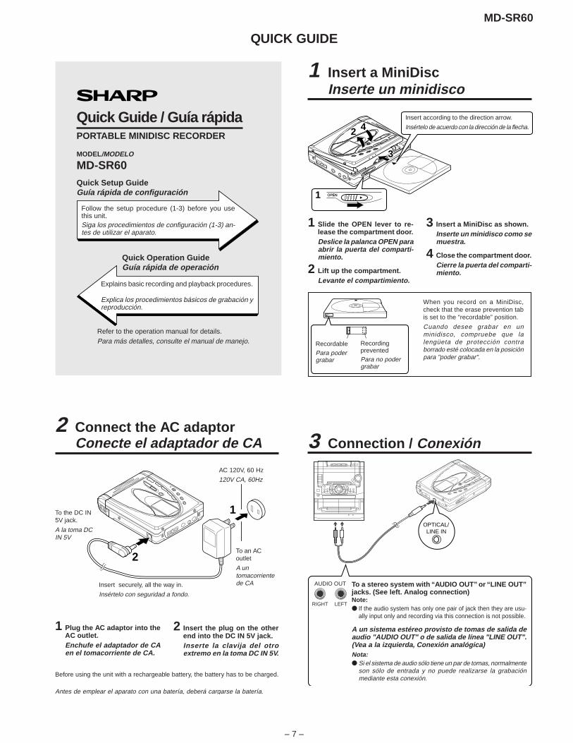
QUICK GUIDE
Quick Guide / Guía rápidaPORTABLE MINIDISC RECORDER
MODEL/MODELO
MD-SR60Quick Setup GuideGuía rápida de configuración
Follow the setup procedure (1-3) before you usethis unit.Siga los procedimientos de configuración (1-3) an-tes de utilizar el aparato.
Quick Operation GuideGuía rápida de operación
Explains basic recording and playback procedures.
Explica los procedimientos básicos de grabación yreproducción.
Refer to the operation manual for details.Para más detalles, consulte el manual de manejo.
1 Insert a MiniDiscInserte un minidisco
1 Slide the OPEN lever to re-lease the compartment door.Deslice la palanca OPEN paraabrir la puerta del comparti-miento.
2 Lift up the compartment.Levante el compartimiento.
2 4
33
1
3 Insert a MiniDisc as shown.Inserte un minidisco como semuestra.
4 Close the compartment door.Cierre la puerta del comparti-miento.
When you record on a MiniDisc,check that the erase prevention tabis set to the “recordable” position.
Cuando desee grabar en unminidisco, compruebe que lalengüeta de protección contraborrado esté colocada en la posiciónpara "poder grabar".
Insert according to the direction arrow.
Insértelo de acuerdo con la dirección de la flecha.
RecordablePara podergrabar
RecordingpreventedPara no podergrabar
2 Connect the AC adaptorConecte el adaptador de CA
To the DC IN5V jack.
A la toma DCIN 5V
2
1
AC 120V, 60 Hz
120V CA, 60Hz
Insert securely, all the way in.
Insértelo con seguridad a fondo.
To an ACoutlet
A untomacorrientede CA
1 Plug the AC adaptor into theAC outlet.Enchufe el adaptador de CAen el tomacorriente de CA.
2 Insert the plug on the otherend into the DC IN 5V jack.Inserte la clavija del otroextremo en la toma DC IN 5V.
Before using the unit with a rechargeable battery, the battery has to be charged.
Antes de emplear el aparato con una batería, deberá cargarse la batería.
OPTICAL/LINE IN
AUDIO OUT
RIGHT LEFT
3 Connection / Conexión
To a stereo system with “AUDIO OUT” or “LINE OUT”jacks. (See left. Analog connection)Note:● If the audio system has only one pair of jack then they are usu-
ally input only and recording via this connection is not possible.
A un sistema estéreo provisto de tomas de salida deaudio "AUDIO OUT" o de salida de línea "LINE OUT".(Vea a la izquierda, Conexión analógica)Nota:● Si el sistema de audio sólo tiene un par de tomas, normalmente
son sólo de entrada y no puede realizarse la grabaciónmediante esta conexión.
MD-SR60
– 8 –
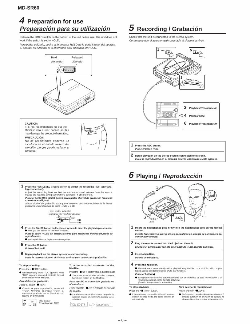
Preparation for usePreparación para su utilizaciónRelease the HOLD switch on the bottom of the unit before use. The unit does notwork if the switch is set to HOLD.
Para poder utilizarlo, suelte el interruptor HOLD de la parte inferior del aparato.El aparato no funciona si el interruptor está colocado en HOLD.
CAUTION:It is not recommended to put theMiniDisc into a rear pocket, as thismay damage the product when sitting.
PRECAUCIÓN:No se recomienda ponerse unminidisco en el bolsillo trasero delpantalón, porque podría dañarlo alsentarse.
Hold
Retenido
Released
Liberado
4Recording / Grabación
Check that the unit is connected to the stereo system.Compruebe que el aparato esté conectado al sistema estéreo.
1
3
5
2 Playback/Reproducción
4 Pause/Pausa
6 Playback/Reproducción
1 Press the REC button.Pulse el botón REC.
2 Begin playback on the stereo system connected to this unit.Inicie la reproducción en el sistema estéreo conectado a este aparato.
5
Recording: continued
To stop recording
Press the • /:OFF button.
When recording stops, “TOC” appears. While“TOC” appears, recorded contents haven’tbeen written on the MiniDisc.
Para detener la grabación:
Pulse el botón • /:OFF.Cuando se pare la grabación, aparecerá"TOC". Mientras aparezca "TOC", elcontenido grabado no se habrá escritotodavía en el minidisco.
TOC displayVisualización TOC
To write recorded contents on theMiniDisc
Press the • /:OFF button while in the stop mode.
The power turns off after recorded contentshave been written on the MiniDisc.
Para escribir el contenido grabado enel minidisco
Pulse el botón • /:OFF estando en el modode parada.
La alimentación se desconecta después dehaberse escrito el contenido grabado en elminidisco.
3 Press the REC LEVEL ( or ) button to adjust the recording level (only ana-log connection).Adjust the recording level so that the maximum sound volume from the sourcemakes the reading swing somewhere between –4 dB and 0 dB.Pulse el botón REC LEVEL ( o ) para ajustar el nivel de grabación (sólo conconexión analógica).Ajuste el nivel de grabación para que el volumen de sonido máximo de la fuenteproduzca una indicación de entre –4 dB y 0 dB.
0dB4dB
4 Press the PAUSE button on the stereo system to enter the playback pause mode.Here you can search for the track to record.
Pulse el botón PAUSE del sistema estéreo para establecer el modo de pausa dereproducción.
Ahora podrá buscar la pista que desee grabar.
5 Press the 06 button.Pulse el botón 06
6 Begin playback on the stereo system to start recording.Inicie la reproducción en el sistema estéreo para comenzar la grabación.
Level meter indicatorIndicador del medidor de nivel
Playing / Reproducción
1 Insert the headphones plug firmly into the headphones jack on the remotecontrol.Inserte firmemente la clavija de los auriculares en la toma de auriculares delcontrolador remoto.
2 Plug the remote control into the jack on the unit.Enchufe el controlador remoto en el enchufe del aparato principal.
3 Insert a MiniDisc.Inserte un minidisco.
4 Press the button.Playback starts automatically with a playback only MiniDisc or a MiniDisc which is pro-
tected against accidental erasure (Auto-play function).
Pulse el botón La reproducción se inicia automáticamente con un minidisco de sólo reproducción o unminidisco protegido contra borrado accidental.(Función de reproducción automática)
To stop playback
Press the • /:OFF button.
If the unit is not operated for at least 2 minuteswhile in the stop mode, the power will shut offautomatically.
To the jack
2
1
4
Para detener la reproducción
Pulse el botón • /:OFF.Si el aparato no se utiliza durante un mínimo de 2minutos estando en el modo de parada, laalimentación se desconectará automáticamente
.
6
MD-SR60
– 9 –
1 Bottom Cabinet 1. Screw ..................... (A1) x6 9-1
2 Top Cabinet 1. Open the Top cabinet. 9-12. Open the Battery Cover.3. Screw ..................... (B1) x44. Flexible PWB.......... (B2) x2 9-2
3 Main PWB 1. Screw .................... (C1) x4 9-22. Flexible PWB......... (C2) x23. Solder joint ............. (C3) x2
4 Mechanism Unit 1. Raise the rear part, and 9-3 remove in the arrow direction.
DISASSEMBLY
Cares before disassemblingWhen assembling the machine after disassembling orrepair, observe the following requirements so as to ensuresafety and performance.1. Remove the batteries from the machine, and take out the
mini-disc.2. When assembling after repair, be sure to position the
wires in the same location.Use the specified screws to fix the cabinet and themechanism unit. The use of the screws with length otherthan specified may cause contact with the mechanismunit resulting in malfunction.
3. When repairing, pay close attention so not to damage theIC from static electricity.
REMOVAL PROCEDURESTEP FIGURE
Figure 9-1
Figure 9-2Figure 9-3
Caution:Carefully handle the main PWB and flexible PWB. After removing theflexible PWB (1*) for the optical pickup from the connector, do nottouch directly the front end of flexible PWB with your hand so as toprevent damage of optical pickup by static electricity.
(B1)x2ø1.4x2mm
(B1)x2ø1.4x2mm
(A1)x1ø1.4x2mm
(A1)x2ø1.4x2mm
(A1)x2ø1.4x2mm
Open Lever
Bottom Cabinet
Top Cabinet
(A1)x1ø1.4x2mm
Battery Cover
Mechanism Unit
(C3)x1(C3)x1
pullpull
pull
pull
pull
pull
Fold back the flexible PWBs to put on the connector, and fix them with felt. Loosening of the flexible PWBs may cause contact withthe sheet metal, resulting in disconnection or short circuit.
Felt
(C1)x4ø1.7x2.5mm
Main PWB
(B2)x2
(C2)x1
(C2)x1*
Mechanism Unit
MD-SR60
– 10 –
REMOVING AND REINSTALLING THE MAIN PARTSRemove the mechanism according to the disassembling meth-ods 1 to 4. (See Page 9.)
How to remove the spindle motor (See Fig. 10-1.)1. Remove the solder joint (A1) x 1 of flexible PWB.2. Remove the screws (A2) x 3 pcs., and remove the spindle
motor.
Figure 10-5
Figure 10-1
Figure 10-2
Figure 10-3
How to reinstall the optical pickup unit(See Fig. 10-5.)1. Remove the screw (E1) x 1 pc.2. Slowly raise the optical pickup.
How to remove the magnetic head (See Fig. 10-4.)1. Remove the screws (D1) x 4 which connects the magnetic
head to the head relay flexible PWB, remove the springwashers (D2) x 2 and remove the soldering joints (D3) x 2.
Note:Mount carefully so as not to damage the magnetic head.
Figure 10-4
How to remove the Lift motor (See Fig. 10-2.)1. Remove the solder joints (B1) x 2 of head up/down motor
lead wire.2. Remove the screw (B2) x 1 pc., and remove the flexible
PWB.3. Remove the screw (B3) x 1 pc., and remove the head up/
down motor.Note:Take care so that the motor gear is not damaged.(If the gear is damaged, noise is caused.)
How to remove the sled motor (See Fig. 10-3.)1. Remove the stop washer (C1) x 1 pc., and remove the drive
gear (C2) x 1 pc.2. Remove the screws (C3) x 2 pcs., and remove the sled
motor.3. Remove the solder joints (C4) x 2 of flexible PWB.Note:Take care so that the motor gear is not damaged.(If the gear is damaged, noise is caused.)
(A2)x3ø1.4x2.8mm
MD Mechanism
Spindle Motor
Mechanism Flexible PWB Solder joint(A1)x1
(B2)x1ø1.4x1.5mm
(B3)x1ø1.4x5.5mm
MD Mechanism
Remove theSolder joint(B1)x2
Lift Motor
(E1)x1ø1.7x3mm
Guide Shaft
Optical Pickup Unit
MD Mechanism
Thrust Plate Spring
Stop Washer(C1)x1
MD Mechanism
Sled Motor
(C3)x2ø1.4x1.2mm
Driver Gear(C2)x1
Mechanism Flexible PWB Solder joint (C4)x2
Solder joint(D3)x2
(D1)x1ø1.4x1.5mm
(D1)x1ø1.2x1.6mm
(D1)x2ø1.4x2.2mm
Magnetic Head
MD Mechanism
(D2)x2Spring joint
MD-SR60
– 11 –
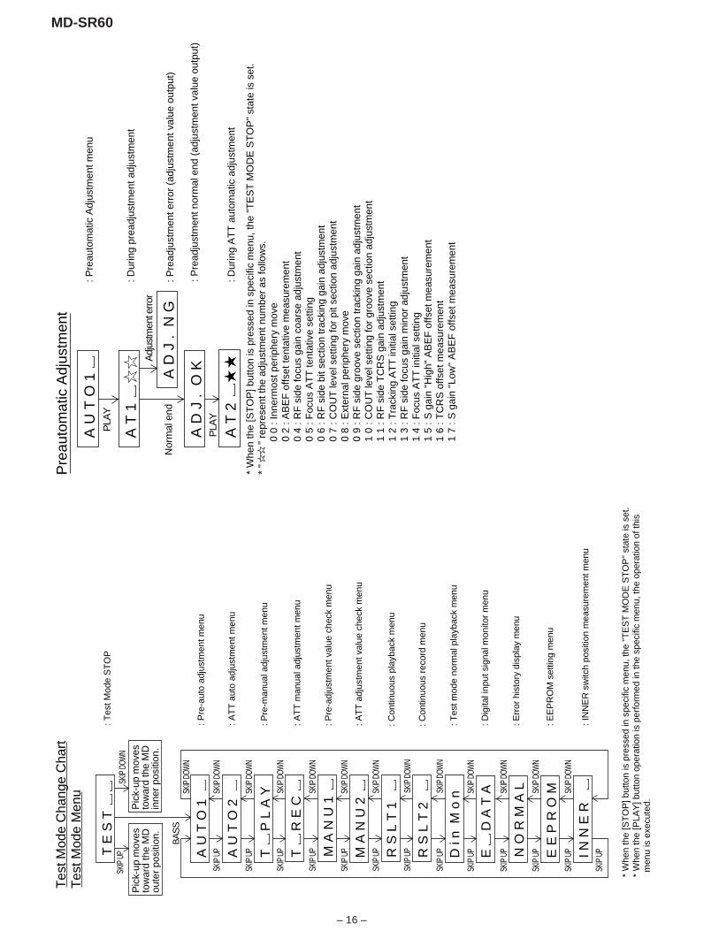
Entering the TEST mode1. Setting at port (power nonconnected state)
(1) Set the port as follows. TEST1 : "Low" (TP416) TEST0 : "High"(2) Turn the Power ON.(3) Test Mode START [ T E S T _ ]
2. Setting by special button operation (in standby state)(1) Holding down the DISP button and ENTER button, press the PLAY button.(2) Normal mode setting initialization (BASS setting, VOL setting, etc.)*Since the unit is changed to the setting for production line inspection , be sure to set it to the default setting state in the following default setting procedure before returning it to the user.(3) Indication of microcomputer version for one second [ Y 1 9 A b X ]
(4) Whole LCD lighting for 2 seconds(5) Test Mode START [ T E S T _ ]*When the PLAY button is pressed during indication (3) and (4), the process proceeds to (5).
1 High reflection disc MMD-110 (TEAC Test MD) 88GMMD-110
2 Low reflection disc MMD-212 (TEAC Test MD) 74-minute disc 88GMMD-212
3 Low reflection disc MMD-213A (TEAC Test MD) 80-minute disc 88GMMD-213A
4 Low reflection disc Recording minidisc UDSKM0001AFZZ
ADJUSTMENT Test discMD adjustment needs two types of disc, namely recording disc (low reflection disc) and playback-only disc (highreflection disc).
Type Test disc Parts No.
Note: Use the low reflection disc on which music has been recorded.
Leaving the TEST mode(1) Press the STOP button in the TEST mode stop state.
Test Mode
Shipping setting methodHolding down simultaneously the VOLUME-DOWN Button and PLAY Button of the set unit without disc, supply the power from the DC IN plug.After the indication "INIT" -> "BYE OK" disappears, release the power supply of DC IN.
1. AUTO 1 Mode • Perform preliminary automatic adjustment.• If the combination of mechanism and pickup PWB has been changed, be sure to start from
AUTO1.2. AUTO 2 Mode • Perform ATT (attenuator) automatic adjustment.
• Perform continuous playback (error rate display, jump test)
3. TEST-PLAY Mode • Continuous playback from the specified address is performed.• 1 line, 10 lines or 384 lines manual jump is
performed.• C1 error rate display (pit section), ADIP error
rate display (groove section)• The temperature correction is performed only when
servo start is performed, but the posture correctionis not performed during continuous playback.
4. TEST-REC Mode • Continuous record from the specified addressis performed.
• Change of record laser output (servo gain isalso changed according to laser output).
• The temperature correction is performed onlywhen servo start is performed, but the posturecorrection is not performed during continuousrecording.
5. MANUAL 1 Mode • Temperature is displayed. (Updating in real time)• Seeing the displayed adjustment value, perform preliminary manual adjustment. (Error rate indication, jump test)
6. MANUAL 2 Mode • Temperature is displayed. (Updating in real time)• Seeing the displayed adjustment value perform
manfully the preliminary adjustment. (Error rate indication, jump test)• Continuous playback is performed (error rate display, jump test).
7. RESULT 1 Mode • The value adjusted in AUTO1 or MANUAL1 is indicated.• (Execution in servo "OFF" state").
8. RESULT 2 Mode • The value adjusted in AUTO 2 or MANUAL 2 is indicated.• Adjustment value is changed manually. (error rate display, jump test).
9. DIGITAL INPUT Mode • Digital input information is displayed.10. ERROR INFORMATION • Error information is displayed. Mode • Error information is initialized11. NORMAL Mode • The mode is changed from the TEST mode to
the normal mode without adjustment.• In the normal mode the internal operation mode,
memory capacity, etc. are indicated.• In the normal mode both temperature correction
and posture correction are performed.12. EEPROM Mode • Factors of digital servo are changed manually.
(Each servo is turned on individually.)• Cutoff frequency of BASS1, BASS2 and BASS3
is selected manually.• Temperature detection terminal voltage is
measured, and the reference value is set.• Defaults are selected and set.• Setting of EEPROM protect area is updated.
(In case of protect releasing)13. INNER Mode • Determine the position where the INNER switch
is turned on. (only high reflection disc).• The temperature correction is performed only
when servo start is performed, but the posturecorrection is not performed.
EEPROM version
Destination
Microcomputer version
MD-SR60
– 12 –
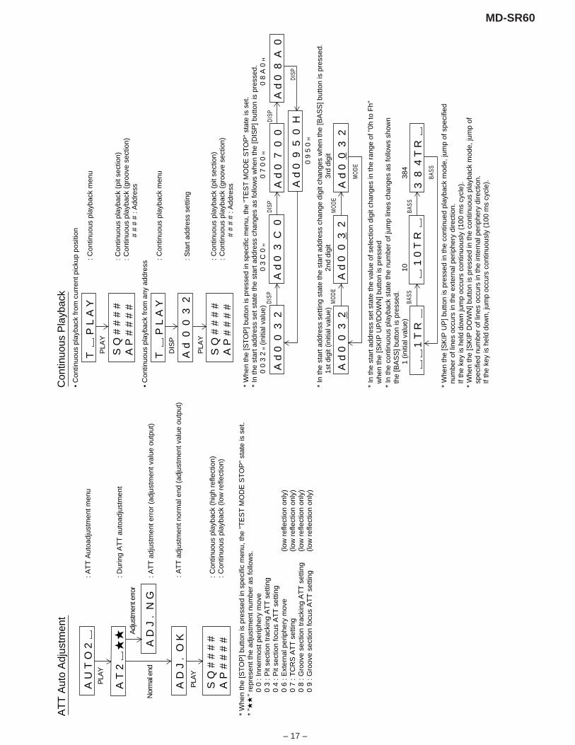
Operation in each TEST mode1. AUTO1 Mode• When the STOP button is pressed while the AUTO1 menu appears or during automatic adjustment, the mode changes to the TEST mode
stop state. At this time the adjustment value is not output.• Be sure to adjust, using the specified disc MMD-213A or MMD-212. At this time release the EEPROM (IC402) protection. (Refer to EEPROM write procedure.)• Adjustment NG; Adjustment item out of range, focus ON failure, and adjustment error• When the PLAY button is pressed while ADJ. OK is displayed, AUTO2 is executed.
2. AUTO2 Mode• When the STOP button is pressed while the AUTO2 menu appears or during automatic adjustment, the mode changes to the TEST mode
stop state. At this time the adjustment value is not output.• Adjustment NG; Adjustment item out of range, and adjustment error.• When the PLAY button is pressed while ADJ. OK is displayed, TEST_PLAY is executed.
3. TEST-PLAY Mode• When the STOP button is pressed while the TEST-PLAY menu appears, or in TEST-PLAY or continuous playback mode, the mode
changes to the TEST mode stop state.• When the PLAY button is pressed while the TEST-PLAY menu appears, continuous playback is initiated from the current pickup position.• Whenever the DISP button is pressed in the TEST-PLAY menu, the target address changes as follows.
0032 — 03C0 — 0700 — 08A0 — 0950— 0032 —When the PLAY button is pressed while a target address is displayed, continuous playback is performed after searching that address.
• Each time the MODE button is pressed while the TEST-PLAY mode target address is displayed, the digit which is changed by pressing theSKIP UP/DOWN button is changed as follows.
0032 — 0032 — 0032 — 0032 —• When the SKIP UP button is pressed in the TEST-PLAY mode target address is displayed, the digit of address specified by the MODE
button is set to +1h. (0 to F)• When the SKIP DOWN button is pressed in the TEST-PLAY mode target address is displayed, the digit of address specified by the MODE
button is set to -1h. (0 to F)* When the SKIP UP/DOWN button is held down, the setting changes continuously, one cycle being 100 ms.
• When the BASS button is pressed in the continuous playback mode, the number of jump lines changes as follows.1 — 10 — 384 — 1
* After the number of jump lines is indicated for one second, the address indication is restored. [ T R _ ]
• When the SKIP UP button is pressed in the continuous playback mode, the specified number of lines is jumped in the FWD direction.• When the SKIP DOWN button is pressed in the continuous playback mode, the specified number of lines is jumped in the REV direction.
* When the SKIP UP/DOWN button is held down, jump is repeated every approx. 100 ms.• Whenever the DISP button is pressed in the continuous playback mode, the indication changes as follows.
* Pre-mastered discContinuous playback (SUBQ address indication) [ S Q ]
|Continuous playback (C1 error indication) [ C E ]
|Continuous playback (SUBQ address indication) [ S Q ]
* Recordable diskContinuous playback (ADIP address indication) [ A P ]
|Continuous playback (C1 error indication) [ C E ]
|Continuous playback (ADIP error indication) [ A E ]
|Continuous playback (ADIP address indication) [ A P ]
4. TEST-REC Mode• When the STOP button is pressed while the TEST-REC menu appears, or in the TEST-REC mode or continuous record mode, the mode
changes to the TEST mode stop state.• When the PLAY button is pressed while the TEST-REC menu appears, the continuous record is initiated from the current pickup position.• Whenever the DISP button is pressed in the TEST-REC menu, the target address changes as follows.
0032 — 03C0 — 0700 — 08A0 —0950 — 0032 —When the PLAY button is pressed while a target address is displayed, continuous playback is performed after searching that address. • Whenever the MODE button is pressed in the TEST-REC mode target address is displayed, the digit which is changed by the SKIP UP/
DOWN button changes as follows.0032 — 0032 — 0032 — 0320 —
• When the SKIP UP button s pressed in the TEST-REC mode target address is displayed, the digit of address specified by the BASS buttonis set to +1h.(0 to F)
• When the SKIP DOWN button is pressed in the TEST-REC mode target address is displayed, the digit of address specified by the BASSbutton is set to -1h. (0 to F)
* When the SKIP UP/DOWN button is held down, the setting changes continuously, one cycle being 100 ms.
MD-SR60
– 13 –
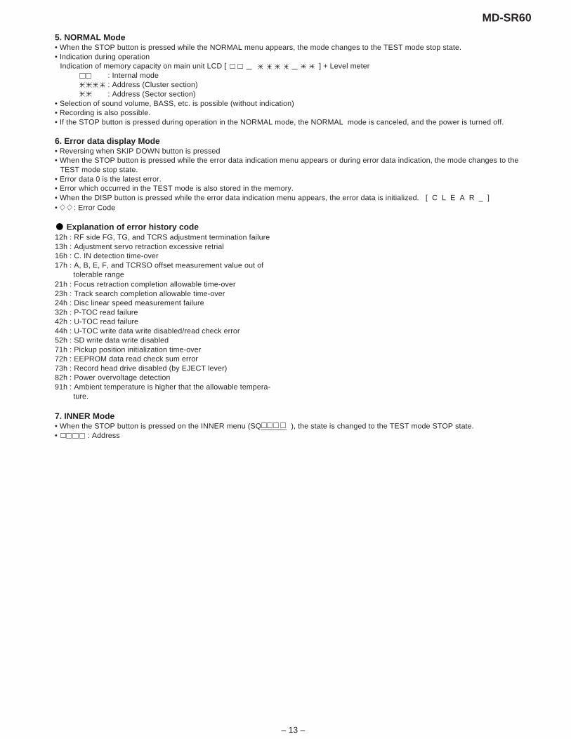
5. NORMAL Mode• When the STOP button is pressed while the NORMAL menu appears, the mode changes to the TEST mode stop state.• Indication during operation
Indication of memory capacity on main unit LCD [ ] + Level meter: Internal mode: Address (Cluster section): Address (Sector section)
• Selection of sound volume, BASS, etc. is possible (without indication)• Recording is also possible.• If the STOP button is pressed during operation in the NORMAL mode, the NORMAL mode is canceled, and the power is turned off.
6. Error data display Mode• Reversing when SKIP DOWN button is pressed• When the STOP button is pressed while the error data indication menu appears or during error data indication, the mode changes to the
TEST mode stop state.• Error data 0 is the latest error.• Error which occurred in the TEST mode is also stored in the memory.• When the DISP button is pressed while the error data indication menu appears, the error data is initialized. [ C L E A R _ ]• : Error Code
Explanation of error history code12h : RF side FG, TG, and TCRS adjustment termination failure13h : Adjustment servo retraction excessive retrial16h : C. IN detection time-over17h : A, B, E, F, and TCRSO offset measurement value out of
tolerable range21h : Focus retraction completion allowable time-over23h : Track search completion allowable time-over24h : Disc linear speed measurement failure32h : P-TOC read failure42h : U-TOC read failure44h : U-TOC write data write disabled/read check error52h : SD write data write disabled71h : Pickup position initialization time-over72h : EEPROM data read check sum error73h : Record head drive disabled (by EJECT lever)82h : Power overvoltage detection91h : Ambient temperature is higher that the allowable tempera-
ture.
7. INNER Mode• When the STOP button is pressed on the INNER menu (SQ______ ), the state is changed to the TEST mode STOP state.• : Address

MD-SR60
– 14 –
EEPROM (IC402) writing procedure1. Procedure to replace EEPROM and write initial value of microcomputer in EEPROM
(1) Replace EEPROM.(2) Refer to the latest EEPROM data list.(3) Press the Display button, ENTER button and Play button to start the test mode.(4) Version display
[ V e r . ]
EEPROM version (b ~ Z)Microcomputer ROM version
(5) The whole LCD lights.(6) Test mode stop state.
[ T E S T ](7) Press the "BASS" button, and press twice the "SKIP DOWN" button.
[ E E P R O M ](8) Perform the operation to display "EEPROM SETTING MODE CHART", compare the EEPROM DATA LIST with the display,
and set according to the EEPROM DATA LIST with the VOL UP or VOL DOWN key. (9) Set the temperature reference. (Refer to the Temperature Reference Setting Method.) (10) Set according to the EEPROM DATA LIST. (11) Press the Stop button.
[ T E S T ] (12) Press the Stop button. (13) After data is written in EEPROM, turn off power . (14) Restore protection of EEPROM.
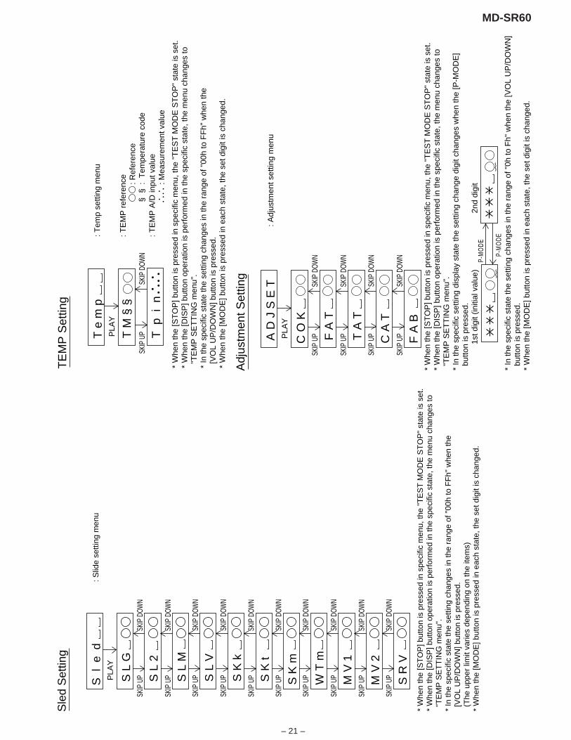
2. Temperature reference setting method[1] Measurement, calculation and setting procedure
(1) Set the TEST mode. • Set TEST 1, 0 = '01', and turn on power (or set PLAY ON in standby state).(2) Start the EEPROM mode 'Temp' menu. • Key operation in order of BASS, SKIP-DOWN x 2 times, PLAY, PLAY in the test mode STOP state. • 'TM$$%%' is displayed. ($$= Temperature code, %% = Temperature reference)(3) Once press SKIP-UP, and determine the displayed microcomputer TEMP input AD value. • 'TPin##' is displayed. (## = TEMP input AD value)(4) At the ambient temperature, determine the temperature corrected value from the temperature measurement value
correction table.(5) Determine the temperature reference, using the following formula. • Temperature reference = Microcomputer TEMP input AD value + Temperature corrected value(6) Set the temperature reference value by button operation , and check whether the temperature code indication corresponds to "Temperature
Code Identification Table".
[2] Temperature measurement value correction table
Ambienttemperature
Temperaturecorrection
+ 9oC ~ +11oC - 05h + 10.0oC
+12oC ~ +14oC - 04h + 12.7oC
+15oC ~ +16oC - 03h + 15.4oC
+17oC ~ +19oC - 02h + 18.2oC
+20oC ~ +22oC - 01h + 20.9oC
+23oC ~ +24oC ± 00h + 23.6oC
+25oC ~ +27oC + 01h + 26.3oC
+28oC ~ +30oC + 02h + 29.0oC
+31oC ~ +33oC + 03h + 31.8oC
Centertemperature
Ambienttemperature
Temperaturecorrection
Centertemperature
- 9oC ~ +10oC 08h + 0.5oC
+ 3oC ~ +21oC 07h + 12.5oC
+15oC ~ +33oC 06h + 23.6oC
+26oC ~ +43oC 05h + 35.0oC
X
– 15 –
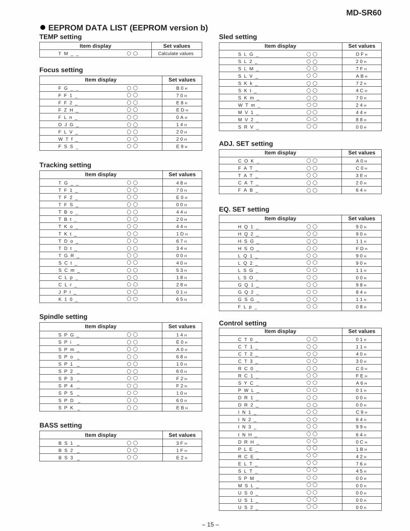
MD-SR60
Sled settingItem display Set values
EEPROM DATA LIST (EEPROM version b)TEMP setting
Item display Set valuesT M _ _ Calculate values
ADJ. SET settingItem display Set values
C O K _ A 0 H
F A T _ C 0 H
T A T _ 3 E H
C A T _ 2 0 H
F A B _ 6 4 H
BASS settingItem display Set values
B S 1 _ 3 F H
B S 2 _ 1 F H
B S 3 _ E 2 H
S L G _ D F H
S L 2 _ 2 0 H
S L M _ 7 F H
S L V _ A B H
S K k _ 7 2 H
S K t _ 4 C H
S K m _ 7 0 H
W T m _ 2 4 H
M V 1 _ 4 4 H
M V 2 _ 8 8 H
S R V _ 0 0 H
EQ. SET settingItem display Set values
H Q 1 _ 9 0 H
H Q 2 _ 9 0 H
H S G _ 1 1 H
H S O _ F D H
L Q 1 _ 9 0 H
L Q 2 _ 9 0 H
L S G _ 1 1 H
L S O _ 0 0 H
G Q 1 _ 9 8 H
G Q 2 _ 8 4 H
G S G _ 1 1 H
F L p _ 0 8 H
Control settingItem display Set values
C T 0 _ 0 1 H
C T 1 _ 1 1 H
C T 2 _ 4 0 H
C T 3 _ 3 0 H
R C 0 _ C 0 H
R C 1 _ F E H
S Y C _ A 6 H
P W L _ 0 1 H
D R 1 _ 0 0 H
D R 2 _ 0 0 H
I N 1 _ C 9 H
I N 2 _ 6 4 H
I N 3 _ 9 9 H
I N H _ 6 4 H
D R H _ 0 C H
P L E _ 1 B H
R C E _ 4 2 H
E L T _ 7 6 H
S L T _ 4 5 H
S P M _ 0 0 H
M S L _ 0 0 H
U S 0 _ 0 0 H
U S 1 _ 0 0 H
U S 2 _ 0 0 H
Item display Set values
F G _ _ B 0 H
F F 1 _ 7 0 H
F F 2 _ E 8 H
F Z H _ E D H
F L n _ 0 A H
D J G _ 1 4 H
F L V _ 2 0 H
W T f _ 2 0 H
F S S _ E 9 H
Focus setting
Tracking settingItem display Set values
T G _ _ 4 8 H
T F 1 _ 7 0 H
T F 2 _ E 0 H
T F S _ 0 0 H
T B o _ 4 4 H
T B t _ 2 0 H
T K o _ 4 4 H
T K t _ 1 D H
T D o _ 6 7 H
T D t _ 3 4 H
T G R _ 0 0 H
S C t _ 4 0 H
S C m _ 5 3 H
C L p _ 1 8 H
C L r _ 2 8 H
J P I _ 0 1 H
K 1 0 _ 6 5 H
Item display Set values
S P G _ 1 4 H
S P i _ E 0 H
S P m _ A 0 H
S P o _ 6 8 H
S P 1 _ 1 0 H
S P 2 _ 6 0 H
S P 3 _ F 2 H
S P 4 _ F 2 H
S P 5 _ 1 0 H
S P D _ 6 0 H
S P K _ E B H
Spindle setting
– 16 –
MD-SR60
: Tes
t Mod
e S
TO
P
: Pre
-aut
o ad
just
men
t men
u
: AT
T a
uto
adju
stm
ent m
enu
: Con
tinuo
us r
ecor
d m
enu
: EE
PR
OM
set
ting
men
u
: IN
NE
R s
witc
h po
sitio
n m
easu
rem
ent m
enu
BA
SS
T E
S T
Pic
k-up
mov
es
tow
ard
the
MD
oute
r po
sitio
n.
Tes
t Mod
e M
enu
Tes
t Mod
e C
hang
e C
hart
A U
T O
1
A U
T O
2SK
IP U
PSK
IP D
OWN
SKIP
DOW
N
SKIP
UP
SKIP
DOW
N
SKIP
UP
SKIP
DOW
N
SKIP
UP
SKIP
DOW
N
SKIP
UP
SKIP
DOW
N
T
R E
C
SKIP
UP
SKIP
DOW
N
: Con
tinuo
us p
layb
ack
men
u
T
P L
A Y
SKIP
UP
SKIP
DOW
N
SKIP
UP
SKIP
DOW
N
SKIP
UP
SKIP
DOW
N
: Dig
ital i
nput
sig
nal m
onito
r m
enu
D i
n M
o n
SKIP
UP
SKIP
DOW
N
E E
P R
O M
SKIP
UP
SKIP
DOW
N
I N N
E R
SK
IP U
P
SKIP
UP
SKIP
DOW
N
SKIP
DOW
NSK
IP U
P
* W
hen
the
[ST
OP
] but
ton
is p
ress
ed in
spe
cific
men
u, th
e "T
ES
T M
OD
E S
TO
P"
stat
e is
set
.*
Whe
n th
e [P
LAY
] but
ton
oper
atio
n is
per
form
ed in
the
spec
ific
men
u, th
e op
erat
ion
of th
is m
enu
is e
xecu
ted.
: Pre
-adj
ustm
ent v
alue
che
ck m
enu
R S
L T
1
: AT
T a
djus
tmen
t val
ue c
heck
men
u
R S
L T
2
: Pre
-man
ual a
djus
tmen
t men
u
M A
N U
1
: AT
T m
anua
l adj
ustm
ent m
enu
M A
N U
2
: Err
or h
isto
ry d
ispl
ay m
enu
E
D A
T A
: Tes
t mod
e no
rmal
pla
ybac
k m
enu
N O
R M
A L
Pic
k-up
mov
es
tow
ard
the
MD
inne
r po
sitio
n.
: Pre
auto
mat
ic A
djus
tmen
t men
u
: Pre
adju
stm
ent e
rror
(ad
just
men
t val
ue o
utpu
t)
: Dur
ing
prea
djus
tmen
t adj
ustm
ent
Adj
ustm
ent e
rror
Nor
mal
end
: Pre
adju
stm
ent n
orm
al e
nd (
adju
stm
ent v
alue
out
put)
: Dur
ing
AT
T a
utom
atic
adj
ustm
ent
PLA
Y
PLA
Y
A U
T O
1
Pre
auto
mat
ic A
djus
tmen
t
A D
J .
O K
A D
J .
N G
A T
2
A T
1
* W
hen
the
[ST
OP
] but
ton
is p
ress
ed in
spe
cific
men
u, th
e "T
ES
T M
OD
E S
TO
P"
stat
e is
set
.*
"
"
repr
esen
t the
adj
ustm
ent n
umbe
r as
follo
ws.
0 0
: Inn
erm
ost p
erip
hery
mov
e0
2 : A
BE
F o
ffset
tent
ativ
e m
easu
rem
ent
0 4
: RF
sid
e fo
cus
gain
coa
rse
adju
stm
ent
0 5
: Foc
us A
TT
tent
ativ
e se
tting
0 6
: RF
sid
e bi
t sec
tion
trac
king
gai
n ad
just
men
t0
7 : C
OU
T le
vel s
ettin
g fo
r pi
t sec
tion
adju
stm
ent
0 8
: Ext
erna
l per
iphe
ry m
ove
0 9
: RF
sid
e gr
oove
sec
tion
trac
king
gai
n ad
just
men
t1
0 : C
OU
T le
vel s
ettin
g fo
r gr
oove
sec
tion
adju
stm
ent
1 1
: RF
sid
e T
CR
S g
ain
adju
stm
ent
1 2
: Tra
ckin
g A
TT
initi
al s
ettin
g1
3 : R
F s
ide
focu
s ga
in m
inor
adj
ustm
ent
1 4
: Foc
us A
TT
initi
al s
ettin
g1
5 : S
gai
n "H
igh"
AB
EF
offs
et m
easu
rem
ent
1 6
: TC
RS
offs
et m
easu
rem
ent
1 7
: S g
ain
"Low
" A
BE
F o
ffset
mea
sure
men
t
– 17 –
MD-SR60
: AT
T A
utoa
djus
tmen
t men
u
: AT
T a
djus
tmen
t err
or (
adju
stm
ent v
alue
out
put)
: Dur
ing
AT
T a
utoa
djus
tmen
t
Adj
ustm
ent e
rror
Nor
mal
end
: AT
T a
djus
tmen
t nor
mal
end
(ad
just
men
t val
ue o
utpu
t)
: Con
tinuo
us p
layb
ack
(hig
h re
flect
ion)
: Con
tinuo
us p
layb
ack
(low
ref
lect
ion)
PLA
Y
PLA
Y
A U
T O
2
AT
T A
uto
Adj
ustm
ent
A D
J .
O K
A D
J .
N G
S Q
# #
# #
A P
# #
# #
A T
2
* W
hen
the
[ST
OP
] but
ton
is p
ress
ed in
spe
cific
men
u, th
e "T
ES
T M
OD
E S
TO
P"
stat
e is
set
.*
"
" r
epre
sent
the
adju
stm
ent n
umbe
r as
follo
ws.
0 0
: Inn
erm
ost p
erip
hery
mov
e0
3 : P
it se
ctio
n tr
acki
ng A
TT
set
ting
0 4
: Pit
sect
ion
focu
s A
TT
set
ting
0 6
: Ext
erna
l per
iphe
ry m
ove
(low
ref
lect
ion
only
)0
7 : T
CR
S A
TT
set
ting
(low
ref
lect
ion
only
)0
8 : G
roov
e se
ctio
n tr
acki
ng A
TT
set
ting
(low
ref
lect
ion
only
)0
9 : G
roov
e se
ctio
n fo
cus
AT
T s
ettin
g(lo
w r
efle
ctio
n on
ly)
: Con
tinuo
us p
layb
ack
men
u
: Con
tinuo
us p
layb
ack
(pit
sect
ion)
: Con
tinuo
us p
layb
ack
(gro
ove
sect
ion)
# #
# #
: Add
ress
: Con
tinuo
us p
layb
ack
(pit
sect
ion)
: Con
tinuo
us p
layb
ack
(gro
ove
sect
ion)
# #
# #
: Add
ress
PLA
Y
T
P
L A
Y
Con
tinuo
us P
layb
ack
S Q
# #
# #
A P
# #
# #
* W
hen
the
[ST
OP
] but
ton
is p
ress
ed in
spe
cific
men
u, th
e "T
ES
T M
OD
E S
TO
P"
stat
e is
set
.*
In th
e st
art a
ddre
ss s
et s
tate
the
star
t add
ress
cha
nges
as
follo
ws
whe
n th
e [D
ISP
] but
ton
is p
ress
ed.
0 0
3 2
H (
initi
al v
alue
)0
3 C
0 H
0 7
0 0
H0
8 A
0 H
A d
0 0
3 2
A d
0 3
C 0
DISP
DISP
A d
0 7
0 0
DISP
DISP
A d
0 8
A 0
* In
the
star
t add
ress
set
ting
stat
e th
e st
art a
ddre
ss c
hang
e di
git c
hang
es w
hen
the
[BA
SS
] but
ton
is p
ress
ed.
1st
dig
it (in
itial
val
ue)
2nd
digi
t3r
d di
git
A d
0 0
3 2
A d
0 0
3 2
MO
DE
MO
DE
A d
0 0
3 2
MO
DE
* In
the
cont
inuo
us p
layb
ack
stat
e th
e nu
mbe
r of
jum
p lin
es c
hang
es a
s fo
llow
s sh
own
the
[BA
SS
] but
ton
is p
ress
ed.
1 (in
itial
val
ue)
1038
4
1 T
R
1 0
T R
BASS
BASS
3 8
4 T
RBA
SS
• C
ontin
uous
pla
ybac
k fr
om c
urre
nt p
icku
p po
sitio
n
: Con
tinuo
us p
layb
ack
men
u
: Sta
rt a
ddre
ss s
ettin
g
DIS
P
T
P
L A
Y
A d
0 0
3 2
PLA
Y
S Q
# #
# #
A P
# #
# #
• C
ontin
uous
pla
ybac
k fr
om a
ny a
ddre
ss
* In
the
star
t add
ress
set
sta
te th
e va
lue
of s
elec
tion
digi
t cha
nges
in th
e ra
nge
of "
0h to
Fh"
w
hen
the
[SK
IP U
P/D
OW
N] b
utto
n is
pre
ssed
* W
hen
the
[SK
IP U
P] b
utto
n is
pre
ssed
in th
e co
ntin
ued
play
back
mod
e, ju
mp
of s
peci
fied
num
ber
of li
nes
occu
rs in
the
exte
rnal
per
iphe
ry d
irect
ion.
If t
he k
ey is
hel
d do
wn
jum
p oc
curs
con
tinuo
usly
(10
0 m
s cy
cle)
.*
Whe
n th
e [S
KIP
DO
WN
] but
ton
is p
ress
ed in
the
cont
inuo
us p
layb
ack
mod
e, ju
mp
of s
peci
fied
num
ber
of li
nes
occu
rs in
the
inte
rnal
per
iphe
ry d
irect
ion.
If t
he k
ey is
hel
d do
wn,
jum
p oc
curs
con
tinuo
usly
(10
0 m
s cy
cle)
. A d
0 9
5 0
H
0 9
5 0
H
– 18 –
MD-SR60
: Con
tinuo
us r
ecor
d m
enu
PLA
Y
T
R E
C
Con
tinuo
us R
ecor
d
A P
# #
# #
* W
hen
the
[ST
OP
] but
ton
is p
ress
ed in
spe
cific
men
u, th
e "T
ES
T M
OD
E S
TO
P"
stat
e is
set
.*
In th
e st
art a
ddre
ss s
et s
tate
the
star
t add
ress
cha
nges
as
follo
ws
whe
n th
e [D
ISP
] but
ton
is p
ress
ed.
• C
ontin
uous
rec
ord
from
the
curr
ent p
icku
p po
sitio
n
: Con
tinuo
us r
ecor
d m
enu
: Sta
rt a
ddre
ss s
ettin
g
: Con
tinuo
us r
ecor
d #
# #
#: A
ddre
ss
: Con
tinuo
us r
ecor
d #
# #
#: A
ddre
ss
PLA
Y
T
R E
C
A d
0 0
3 2
PLA
Y
A P
# #
# #
• C
ontin
uous
rec
ord
play
back
from
any
add
ress
A d
0 0
3 2
0
0 3
2 H
(in
itial
val
ue)
0 3
C 0
H0
7 0
0 H
0 8
A 0
H
A d
0 3
c 0
DISP
A d
0 7
0 0
DISP
DISP
DISPA
d 0
8 A
0
* In
the
star
t add
ress
set
ting
stat
e th
e st
art a
ddre
ss c
hang
e di
git c
hang
es w
hen
the
[BA
SS
] but
ton
is p
ress
ed.
A d
0 0
3 2
1st d
igit
(initi
al v
alue
)2n
d di
git
3rd
digi
t
A d
0 0
3 2
MOD
EA
d 0
0 3
2M
ODE
MOD
E
A d
0 9
5 0
: IN
NE
R s
witc
h po
sitio
n m
easu
rem
ent m
enu
: Con
tinuo
us p
layb
ack
(pit
sect
ion)
# #
# #
: Add
ress
PLA
Y
I N
N E
R
Inne
r S
witc
h P
ositi
on M
easu
rem
ent
S Q
# #
# #
* W
hen
the
[ST
OP
] but
ton
is p
ress
ed in
spe
cific
men
u, th
e "T
ES
T M
OD
E S
TO
P"
stat
e is
set
.
: TE
ST
mod
e no
rmal
pla
ybac
k m
enu
: Con
tinuo
us p
layb
ack
@@
@@
@@
: Mod
e an
d ad
dres
s di
spla
y
PLA
Y
N O
R M
A L
Tes
t Mod
e N
orm
al P
layb
ack
@@
@@
@@
* W
hen
the
[ST
OP
] but
ton
is p
ress
ed in
spe
cific
men
u, th
e "T
ES
T M
OD
E S
TO
P"
stat
e is
set
.*
Whe
n th
e N
OR
MA
L m
ode
is c
ance
lled,
the
pow
er is
turn
ed o
ff.
: Err
or h
isto
ry d
ispl
ay m
enu
: Err
or h
isto
ry 0
dis
play
§ §
: Err
or c
ode
: Err
or h
isto
ry 1
dis
play
§ §
: Err
or c
ode
: Err
or h
isto
ry 2
dis
play
§ §
: Err
or c
ode
: Err
or h
isto
ry 3
dis
play
§ §
: Err
or c
ode
: Err
or h
isto
ry 4
dis
play
§ §
: Err
or c
ode
: Err
or h
isto
ry 5
dis
play
§ §
: Err
or c
ode
: Err
or h
isto
ry 6
dis
play
§ §
: Err
or c
ode
: Err
or h
isto
ry 7
dis
play
§ §
: Err
or c
ode
: Err
or h
isto
ry 8
dis
play
§ §
: Err
or c
ode
: Err
or h
isto
ry 9
dis
play
§ §
: Err
or c
ode
PLA
Y
E
D A
T A
Err
or H
isto
ry D
ispl
ay
E 0
§ §
E 1
§ §
: Err
or h
isto
ry d
ispl
ay m
enu
: Err
or h
isto
ry c
lear
DIS
PLA
Y
E
D A
T A
C L
E A
R
SKIP
UP
SKIP
DOW
N
E 2
§ §
SKIP
UP
SKIP
DOW
N
E 3
§ §
SKIP
UP
SKIP
DOW
N
E 4
§ §
SKIP
UP
SKIP
DOW
N
E 5
§ §
SKIP
UP
SKIP
DOW
N
E 6
§ §
SKIP
UP
SKIP
DOW
N
E 7
§ §
SKIP
UP
SKIP
DOW
N
E 8
§ §
SKIP
UP
SKIP
DOW
N
E 9
§ §
SKIP
UP
SKIP
DOW
N
• E
rror
his
tory
cle
ar
• E
rror
his
tory
dis
play
* W
hen
the
[ST
OP
] but
ton
is p
ress
ed in
spe
cific
men
u, th
e "T
ES
T M
OD
E S
TO
P"
stat
e is
set
.

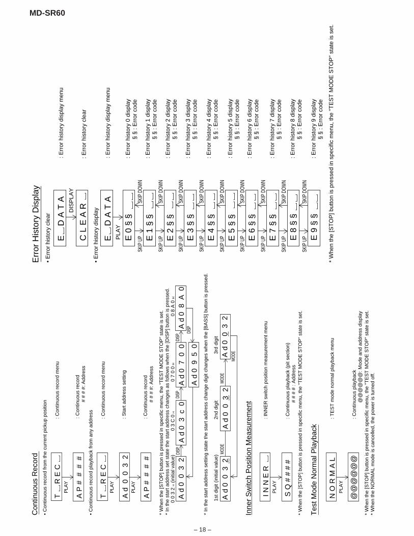
– 19 –
MD-SR60
: EE
PR
OM
set
ting
men
u
: Foc
us s
ettin
g m
enu
: Spi
n se
tting
men
u
: Tra
ckin
g se
tting
men
u
: Sle
d se
tting
men
u
: BA
SS
set
ting
men
u
: TE
MP
set
ting
men
u
: Adj
ustm
ent s
ettin
g m
enu
: Dig
ital E
Q s
ettin
g m
enu
: Con
trol
set
ting
men
u
PLA
Y
E E
P R
O M
EE
PR
OM
Set
ting
F o
c u
s
S p
i n
SKIP
UP
SKIP
DOW
N
T r
a c
kSK
IP U
PSK
IP D
OWN
S l
e d
SKIP
UP
SKIP
DOW
N
B a
s s
SKIP
UP
SKIP
DOW
N
T E
M P
SKIP
UP
SKIP
DOW
N
A D
J S
E T
SKIP
UP
SKIP
DOW
N
D E
Q S
E T
SKIP
UP
SKIP
DOW
N
C T
R L
SKIP
UP
SKIP
DOW
NSK
IP U
P
SKIP
DOW
N
* W
hen
the
[ST
OP
] but
ton
is p
ress
ed in
spe
cific
men
u, th
e "T
ES
T M
OD
E S
TO
P"
stat
e is
set
.*
Whe
n th
e [P
LAY
] but
ton
oper
atio
n is
per
form
ed in
the
spec
ific
stat
e, th
e sp
ecifi
c se
tting
men
u is
set
.
: BA
SS
set
ting
men
u
PLA
Y
B a
s s
BA
SS
Set
ting
B S
1
B S
2SK
IP U
PSK
IP D
OWN
B S
3SK
IP U
PSK
IP D
OWN
* W
hen
the
[ST
OP
] but
ton
is p
ress
ed in
spe
cific
men
u, th
e "T
ES
T M
OD
E S
TO
P"
stat
e is
set
.*
Whe
n th
e [D
ISP
] but
ton
oper
atio
n is
per
form
ed in
the
spec
ific
stat
e, th
e m
enu
chan
ges
to
"T
EM
P S
ET
TIN
G m
enu"
.*
In th
e sp
ecifi
c st
ate
the
setti
ng c
hang
es in
the
rang
e of
"00
h to
FF
h" w
hen
the
[V
OL
UP
/DO
WN
] but
ton
is p
ress
ed.
(T
he u
pper
lim
it va
ries
depe
ndin
g on
the
item
s)*
Whe
n th
e [M
OD
E] b
utto
n is
pre
ssed
in e
ach
stat
e, th
e se
t dig
it is
cha
nged
.
: Foc
us s
ettin
g m
enu
PLA
Y
F o
c u
s
Foc
us S
ettin
g
F G
F F
1SK
IP U
PSK
IP D
OWN
F F
2SK
IP U
PSK
IP D
OWN
F Z
HSK
IP U
PSK
IP D
OWN
F L
nSK
IP U
PSK
IP D
OWN
D J
GSK
IP U
PSK
IP D
OWN
SKIP
UP
SKIP
DOW
N
F L
V
W T
fSK
IP U
PSK
IP D
OWN
* W
hen
the
[ST
OP
] but
ton
is p
ress
ed in
spe
cific
men
u, th
e "T
ES
T M
OD
E S
TO
P"
stat
e is
set
.*
Whe
n th
e [D
ISP
] but
ton
oper
atio
n is
per
form
ed in
the
spec
ific
stat
e, th
e m
enu
chan
ges
to "
TE
MP
SE
TT
ING
men
u".
* In
spe
cific
sta
te th
e se
tting
cha
nged
in th
e ra
nge
of "
00h
to F
Fh"
whe
n th
e [V
OL
UP
/DO
WN
] but
ton
is p
ress
ed.
(T
he u
pper
lim
it va
ries
depe
ndin
g on
the
item
s)*
Whe
n th
e [M
OD
E] b
utto
n is
pre
ssed
in e
ach
stat
e, th
e se
t dig
it is
cha
nged
.
F S
SSK
IP U
PSK
IP D
OWN

– 20 –
MD-SR60
: Spi
n se
tting
men
u
PLA
Y
S p
i n
Spi
n S
ettin
g
S P
G
S P
iSK
IP U
PSK
IP D
OWN
S P
mSK
IP U
PSK
IP D
OWN
S P
oSK
IP U
PSK
IP D
OWN
S P
1SK
IP U
PSK
IP D
OWN
S P
2SK
IP U
PSK
IP D
OWN
S P
3SK
IP U
PSK
IP D
OWN
S P
4SK
IP U
PSK
IP D
OWN
S P
5SK
IP U
PSK
IP D
OWN
S P
DSK
IP U
PSK
IP D
OWN
* W
hen
the
[ST
OP
] but
ton
is p
ress
ed in
spe
cific
men
u, th
e "T
ES
T M
OD
E S
TO
P"
stat
e is
set
.*
Whe
n th
e [D
ISP
] but
ton
oper
atio
n is
per
form
ed in
the
spec
ific
stat
e, th
e m
enu
chan
ges
to "
TE
MP
SE
TT
ING
men
u".
* In
spe
cific
sta
te th
e se
tting
cha
nged
in th
e ra
nge
of "
00h
to F
Fh"
whe
n th
e [
VO
L U
P/D
OW
N] b
utto
n is
pre
ssed
. (
The
upp
er li
mit
varie
s de
pend
ing
on th
e ite
ms)
S P
KSK
IP U
PSK
IP D
OWN
* W
hen
the
[MO
DE
] but
ton
is p
ress
ed in
eac
h st
ate,
the
set d
igit
is c
hang
ed.
: Tra
ckin
g se
tting
men
u
PLA
Y
T r
a c
k
Tra
ckin
g S
ettin
g
T G
T F
1SK
IP U
PSK
IP D
OWN
T F
2SK
IP U
PSK
IP D
OWN
T F
SSK
IP U
PSK
IP D
OWN
T B
oSK
IP U
PSK
IP D
OWN
T B
tSK
IP U
PSK
IP D
OWN
T K
oSK
IP U
PSK
IP D
OWN
T K
tSK
IP U
PSK
IP D
OWN
T D
oSK
IP U
PSK
IP D
OWN
T D
tSK
IP U
PSK
IP D
OWN
* W
hen
the
[ST
OP
] but
ton
is p
ress
ed in
spe
cific
men
u, th
e "T
ES
T M
OD
E S
TO
P"
stat
e is
set
.*
Whe
n th
e [D
ISP
] but
ton
oper
atio
n is
per
form
ed in
the
spec
ific
stat
e, th
e m
enu
chan
ges
to "
TE
MP
SE
TT
ING
men
u".
* In
the
spec
ific
stat
e th
e se
tting
cha
nges
in th
e ra
nge
of "
00h
to F
Fh"
whe
n th
e [V
OL
UP
/DO
WN
] b
utto
n is
pre
ssed
. (T
he u
pper
lim
it va
ries
depe
ndin
g on
the
item
s)
T G
RSK
IP U
PSK
IP D
OWN
S C
tSK
IP U
PSK
IP D
OWN
S C
mSK
IP U
PSK
IP D
OWN
C L
pSK
IP U
PSK
IP D
OWN
C L
rSK
IP U
PSK
IP D
OWN
J P
ISK
IP U
PSK
IP D
OWN
K 1
0SK
IP U
PSK
IP D
OWN
* W
hen
the
[MO
DE
] but
ton
is p
ress
ed in
eac
h st
ate,
the
set d
igit
is c
hang
ed.
– 21 –
MD-SR60
: Slid
e se
tting
men
u
PLA
Y
S l
e d
Sle
d S
ettin
g
S L
G
S L
2SK
IP U
PSK
IP D
OWN
S L
MSK
IP U
PSK
IP D
OWN
S L
VSK
IP U
PSK
IP D
OWN
S K
kSK
IP U
PSK
IP D
OWN
S K
tSK
IP U
PSK
IP D
OWN
S K
mSK
IP U
PSK
IP D
OWN
* W
hen
the
[ST
OP
] but
ton
is p
ress
ed in
spe
cific
men
u, th
e "T
ES
T M
OD
E S
TO
P"
stat
e is
set
.*
Whe
n th
e [D
ISP
] but
ton
oper
atio
n is
per
form
ed in
the
spec
ific
stat
e, th
e m
enu
chan
ges
to "
TE
MP
SE
TT
ING
men
u".
* In
the
spec
ific
stat
e th
e se
tting
cha
nges
in th
e ra
nge
of "
00h
to F
Fh"
whe
n th
e [
VO
L U
P/D
OW
N] b
utto
n is
pre
ssed
. (
The
upp
er li
mit
varie
s de
pend
ing
on th
e ite
ms)
* W
hen
the
[MO
DE
] but
ton
is p
ress
ed in
eac
h st
ate,
the
set d
igit
is c
hang
ed.
W T
mSK
IP U
PSK
IP D
OWN
M V
1SK
IP U
PSK
IP D
OWN
M V
2SK
IP U
PSK
IP D
OWN
S R
VSK
IP U
PSK
IP D
OWN
: Tem
p se
tting
men
u
: TE
MP
ref
eren
ce : Ref
eren
ce
§ §
: T
empe
ratu
re c
ode
: TE
MP
A/D
inpu
t val
ue: M
easu
rem
ent v
alue
PLA
Y
T e
m p
TE
MP
Set
ting
T M
§ §
T p
i n
SKIP
UP
SKIP
DOW
N
* W
hen
the
[ST
OP
] but
ton
is p
ress
ed in
spe
cific
men
u, th
e "T
ES
T M
OD
E S
TO
P"
stat
e is
set
.*
Whe
n th
e [D
ISP
] but
ton
oper
atio
n is
per
form
ed in
the
spec
ific
stat
e, th
e m
enu
chan
ges
to "
TE
MP
SE
TT
ING
men
u".
* In
the
spec
ific
stat
e th
e se
tting
cha
nges
in th
e ra
nge
of "
00h
to F
Fh"
whe
n th
e [
VO
L U
P/D
OW
N] b
utto
n is
pre
ssed
.*
Whe
n th
e [M
OD
E] b
utto
n is
pre
ssed
in e
ach
stat
e, th
e se
t dig
it is
cha
nged
.
: Adj
ustm
ent s
ettin
g m
enu
PLA
Y
A D
J S
E T
Adj
ustm
ent S
ettin
g
C O
K
F A
TSK
IP U
PSK
IP D
OWN
T A
TSK
IP U
PSK
IP D
OWN
C A
TSK
IP U
PSK
IP D
OWN
F A
BSK
IP U
PSK
IP D
OWN
* W
hen
the
[ST
OP
] but
ton
is p
ress
ed in
spe
cific
men
u, th
e "T
ES
T M
OD
E S
TO
P"
stat
e is
set
.*
Whe
n th
e [D
ISP
] but
ton
oper
atio
n is
per
form
ed in
the
spec
ific
stat
e, th
e m
enu
chan
ges
to "
TE
MP
SE
TT
ING
men
u".
* In
the
spec
ific
setti
ng d
ispl
ay s
tate
the
setti
ng c
hang
e di
git c
hang
es w
hen
the
[P-M
OD
E]
but
ton
is p
ress
ed.
1st d
igit
(initi
al v
alue
)2n
d di
git
P-M
ODE
P-M
ODE
* In
the
spec
ific
stat
e th
e se
tting
cha
nges
in th
e ra
nge
of "
0h to
Fh"
whe
n th
e [V
OL
UP
/DO
WN
] b
utto
n is
pre
ssed
.*
Whe
n th
e [M
OD
E] b
utto
n is
pre
ssed
in e
ach
stat
e, th
e se
t dig
it is
cha
nged
.
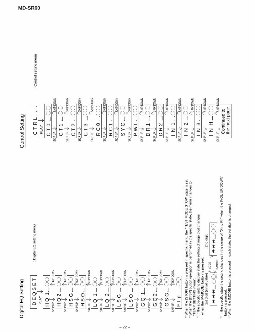
– 22 –
MD-SR60
: Dig
ital E
Q s
ettin
g m
enu
PLA
Y
D E
Q S
E T
Dig
ital E
Q S
ettin
g
H Q
1
H Q
2SK
IP U
PSK
IP D
OWN
H S
GSK
IP U
PSK
IP D
OWN
H S
OSK
IP U
PSK
IP D
OWN
L Q
1SK
IP U
PSK
IP D
OWN
L Q
2SK
IP U
PSK
IP D
OWN
L S
GSK
IP U
PSK
IP D
OWN
L S
OSK
IP U
PSK
IP D
OWN
G Q
1SK
IP U
PSK
IP D
OWN
F L
pSK
IP U
PSK
IP D
OWN
G Q
2SK
IP U
PSK
IP D
OWN
G S
GSK
IP U
PSK
IP D
OWN
* W
hen
the
[ST
OP
] but
ton
is p
ress
ed in
spe
cific
men
u, th
e "T
ES
T M
OD
E S
TO
P"
stat
e is
set
.*
Whe
n th
e [D
ISP
] but
ton
oper
atio
n is
per
form
ed in
the
spec
ific
stat
e, th
e m
enu
chan
ges
to "
TE
MP
SE
TT
ING
men
u".
* In
the
spec
ific
setti
ng d
ispl
ay s
tate
the
setti
ng c
hang
e di
git c
hang
es
w
hen
the
[P-M
OD
E] b
utto
n is
pre
ssed
. 1
st d
igit
(initi
al v
alue
)
2nd
dig
itP-
MO
DE
P-M
ODE
* In
the
spec
ific
stat
e th
e se
tting
cha
nges
in th
e ra
nge
of "
0h to
Fh"
whe
n th
e [V
OL
UP
/DO
WN
] b
utto
n is
pre
ssed
.*
Whe
n th
e [M
OD
E] b
utto
n is
pre
ssed
in e
ach
stat
e, th
e se
t dig
it is
cha
nged
.
: Con
trol
set
ting
men
u
PLA
Y
C T
R L
Con
trol
Set
ting
C T
0
C T
1SK
IP U
PSK
IP D
OWN
C T
2SK
IP U
PSK
IP D
OWN
C T
3SK
IP U
PSK
IP D
OWN
R C
0SK
IP U
PSK
IP D
OWN
R C
1SK
IP U
PSK
IP D
OWN
S Y
CSK
IP U
PSK
IP D
OWN
P W
LSK
IP U
PSK
IP D
OWN
D R
1SK
IP U
PSK
IP D
OWN
D R
2SK
IP U
PSK
IP D
OWN
I N
1SK
IP U
PSK
IP D
OWN
I N
2SK
IP U
PSK
IP D
OWN
I N
3SK
IP U
PSK
IP D
OWN
I N
HSK
IP U
PSK
IP D
OWN
Con
tinue
d to
th
e ne
xt p
age
SKIP
UP
SKIP
DOW
N
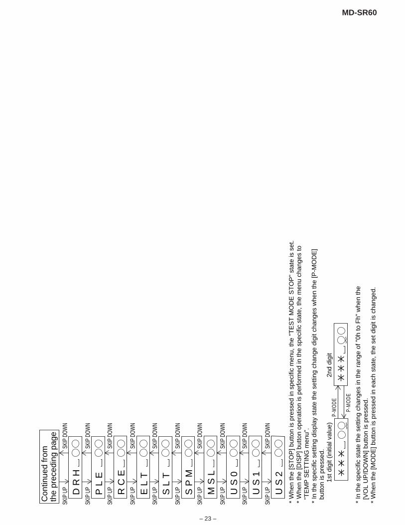
– 23 –
MD-SR60
Con
tinue
d fr
om
the
prec
edin
g pa
ge
D R
HSK
IP U
PSK
IP D
OWN
P L
ESK
IP U
PSK
IP D
OWN
SKIP
UP
SKIP
DOW
N
SKIP
UP
SKIP
DOW
N
R C
E
E L
T
S L
TSK
IP U
PSK
IP D
OWN
S P
MSK
IP U
PSK
IP D
OWN
SKIP
UP
SKIP
DOW
N
SKIP
UP
SKIP
DOW
N
M S
L
U S
0SK
IP U
PSK
IP D
OWN
SKIP
UP
SKIP
DOW
N
U S
1
U S
2*
Whe
n th
e [S
TO
P] b
utto
n is
pre
ssed
in s
peci
fic m
enu,
the
"TE
ST
MO
DE
ST
OP
" st
ate
is s
et.
* W
hen
the
[DIS
P] b
utto
n op
erat
ion
is p
erfo
rmed
in th
e sp
ecifi
c st
ate,
the
men
u ch
ange
s to
"T
EM
P S
ET
TIN
G m
enu"
.*
In th
e sp
ecifi
c se
tting
dis
play
sta
te th
e se
tting
cha
nge
digi
t cha
nges
whe
n th
e [P
-MO
DE
] b
utto
n is
pre
ssed
.1s
t dig
it (in
itial
val
ue)
2nd
digi
tP-
MO
DE
P-M
ODE
* In
the
spec
ific
stat
e th
e se
tting
cha
nges
in th
e ra
nge
of "
0h to
Fh"
whe
n th
e [
VO
L U
P/D
OW
N] b
utto
n is
pre
ssed
.*
Whe
n th
e [M
OD
E] b
utto
n is
pre
ssed
in e
ach
stat
e, th
e se
t dig
it is
cha
nged
.
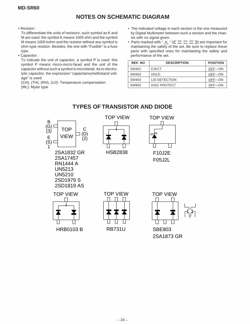
– 24 –
MD-SR60
SW401 EJECT OFF—ON
SW402 HOLD OFF—ON
SW403 LID DETECTION OFF—ON
SW902 DISC PROTECT OFF—ON
NOTES ON SCHEMATIC DIAGRAM
• Resistor:To differentiate the units of resistors, such symbol as K andM are used: the symbol K means 1000 ohm and the symbolM means 1000 kohm and the resistor without any symbol isohm-type resistor. Besides, the one with “Fusible” is a fusetype.
• Capacitor:To indicate the unit of capacitor, a symbol P is used: thissymbol P means micro-micro-farad and the unit of thecapacitor without such a symbol is microfarad. As to electro-lytic capacitor, the expression “capacitance/withstand volt-age” is used.(CH), (TH), (RH), (UJ): Temperature compensation(ML): Mylar type
• The indicated voltage in each section is the one measuredby Digital Multimeter between such a section and the chas-sis with no signal given.
• Parts marked with “ ” ( ) are important formaintaining the safety of the set. Be sure to replace theseparts with specified ones for maintaining the safety andperformance of the set.
POSITIONREF. NO DESCRIPTION
HRB0103 B
2SA1832 GR2SA17457RN1444 AUN5213UN52102SD1979 S2SD1819 AS
TOPVIEW
TOP VIEW
F10J2EF05J2L
TOP VIEWB
(G)(3)E
(S)1
C(D)(2)
HSB2838
TOP VIEW
SBE8032SA1873 GR
TOP VIEW
RB731U
TOP VIEW
TYPES OF TRANSISTOR AND DIODE
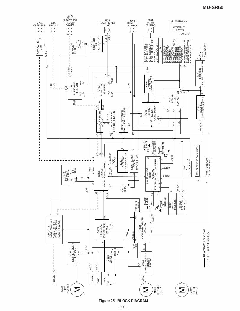
– 25 –
MD-SR60
Figure 25 BLOCK DIAGRAM
IC65
1M
OT
OR
DR
IVE
RLB
1930
M V
CC
VC
C
V
EE
IC84
1 63
72C
281
2.8V
UP
CO
NV
ER
TE
RIC25
1 F
TD
2017
IC25
3 R
N49
04IC
255
NJM
022V
IC25
6 R
N49
11IC
257
S80
808L
NIC
258
259
HN
1C01
FU
IC26
0 R
N49
04IC
809
RN
4904
IC89
2 H
N1C
01F
UT
RA
NS
IST
OR
,P
OW
ER
TR
AN
SIS
TOR
,N
-ch
MO
S F
ET
,D
IGIT
AL
TRA
NS
ISTO
R,
OP
AM
P,R
ES
ET
M90
3LI
FT
MO
TO
R
IC84
2X
C62
HS
022.
35V
RE
GU
LAT
OR
IC82
2IR
3M14
ND
C/D
CC
ON
VE
RT
ER
IC50
1A
D/D
A C
ON
VE
RTE
RA
K45
50V
T
M90
2S
LED
MO
TO
R
IC10
1R
F S
IGN
AL
PR
OC
ES
SO
RIR
3R55
IC77
1 6
2GR
2522
2.5V
RE
GU
LAT
OR
IC40
1IX
0341
AW
SY
ST
EM
MIC
RO
CO
MP
UT
ER
RIP
PLE
FIL
TE
R
VC
C
VE
E
IC87
362
GR
4522
4.5V
RE
GU
LAT
OR
OP
IC
LAS
ER
PIC
K
HE
AD
M90
1S
PIN
DLE
MO
TO
R
IC20
1LR
3781
1E
ND
EC
/SE
RV
O/A
TR
AC
+2.
7V
+2.
5V
T
F
+2.
5V
+2.
7V
VD
D+
2.0V
AV
CC
+2.
5V
+7V
+2.
5V
J703HEADPHONES
LINE
J703REMOTE
CONTROL
IC80
1 62
RP
2002
IC80
2 H
N1C
01F
UIC
803
S80
819L
NP
OW
ER
TR
AN
SIS
TOR
,R
ES
ET
IC,
2V R
EG
ULA
TO
R
J801DC IN
(4~5.5V)
1.0-1.7V
+2.
35V
LCD
AS
S'Y
KE
Y F
LEX
IBLE
PW
B A
SS
'Y
IC90
1S
PIN
DLE
MO
TO
R D
RIV
ER
LB19
71V
IC70
3A
UD
IO A
MP
.IR
3R59
N
IC70
1A
UD
IO A
MP
.IR
3R54
N
IC60
14-
CH
PW
M D
RIV
ER
LV80
17W
IC40
2E
EP
RO
M
58X
2402
T
IC20
2IX
2567
AF
4M
D-R
AM
+2.
5V
OP
TIC
AL
INU
NIT
J701OPTICAL IN
J701LINE IN
J702MIC IN
(READY FOR PLUG/INPOWER)
IC20
362
FP
2002
2V R
EG
ULA
TO
R
1,2,
21,2
36
5,7
7,30
,35
VC
CV
G
43
16,1
8,20
,22
39,4
117
,21,
27,
40,4
4
13,1
424
,42
40
26-2
9,32
-37,
39-4
6
1-9,
11-1
97,
9
66
749
2,3
15,1
6
4,21
2017
9,16
7,18
10,1
2
624
L-
CH
22
R-C
H
17
Q72
1
1-2
2,13
,14,
24,
25,3
6,37
6-9
1-12
1,5,
6,714
-17
55,
59,
81,
82
9, 11,
13,
48
50,7
5,83
74
2
18-2
450
5
52
5
8
3
10
+2.
7V
82-8
4,86
,89
-100
12,6
2,68
,87
3
4
2
2
5,6
N.C
.
SW
402
HO
LD
SW
902
DIS
CP
RO
TE
CT
95 4
SW
401
EJE
CT
SW
403
LID
DE
TEC
TIO
N
19
40,5
7,58
,61,
63,
64,6
5,77
,78,
98
738
PLA
YB
AC
K S
IGN
AL
RE
CO
RD
SIG
NA
L+
B
M MM
6
Ni - MH Batteryor
Dry Battery(1 pieces)
+2.
7V
1, 2
0-30
, 73,
33-
35
R-C
H
2 3
L-C
H 4
3
VC
C
L-C
H
5
8R
-CH
3
NO
R G
AT
EIC
351
74A
CT
02T
N-c
h M
OS
FE
TIC
354
CP
H56
08IC
353
FT
D20
05
IC85
2IR
3M14
ND
C/D
CC
ON
VE
RT
ER
F84
10.
4A,D
C 6
0V
2
2
2
VC
C
2,3
+2V
+1-2V
1
+2.
5V
IC43
1R
ES
ET
S80
820L
N
1
62
IC62
1 R
N49
04D
IGIT
AL
TR
AN
SIS
TO
R
16
5
+2.
5V
-2.5
V
+4.
0V
3
5,6
IC85
1C
PH
3403
N-c
h M
OS
FE
T
IC87
1 T
C7S
86F
UE
XC
LUS
IVE
OR
GA
TTE
17
3
2,4
1,7
1,7
IC82
1 C
PH
3403
N-c
h M
OS
FE
T
VC
C
31
LAS
ER
ON
/OF
F Q10
1
4
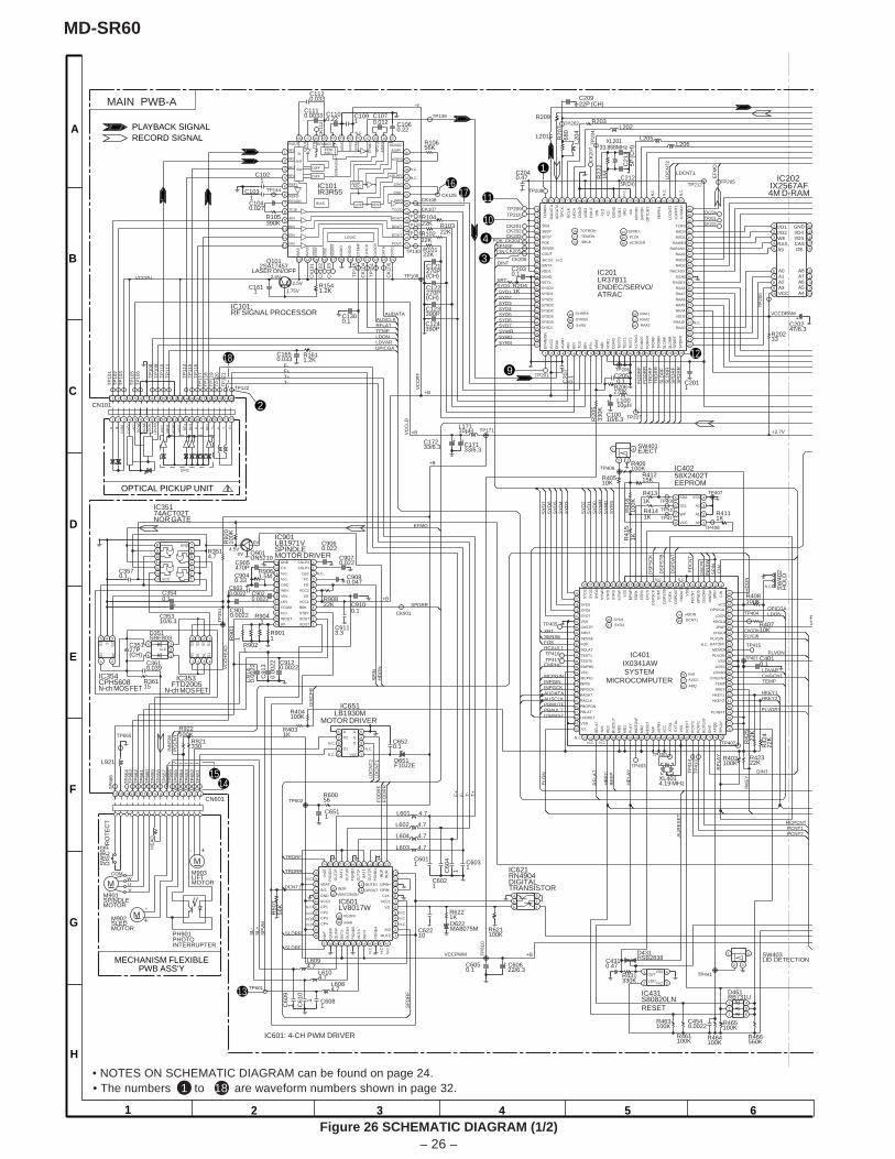
– 26 –
MD-SR60
• The numbers 1 to 18 are waveform numbers shown in page 32.
A
B
C
D
E
F
G
H
1 2 3 4 5 6Figure 26 SCHEMATIC DIAGRAM (1/2)
• NOTES ON SCHEMATIC DIAGRAM can be found on page 24.
22 21 20 19 18 17 16 15 14 13 12 11 10 9 8 7 6 5 4 3 2 1
TP
610
CK901
TP601
48 47 46 45 44 43 42 41 40 39 38 37
36
35
34
33
32
31
30
29
28
27
26
25
24 23 22 21 20 19 18 17 16 15 14 13
12 11 10 9 8
7 6
5 4 3 2 1
TP602
6 5
4 3 2 1
TP407
4
3 2
1
8
7
6
5 4
3
2
1
TP410
TP408
TP409
TP411
10
9 8 7
6 5 4 3 2 1
TP441
4
3 2
1
24
23
22
21
20
19
18
17
16
15 14
13 12 11 10 9 8
7 6
5 4 3 2 1
TP207
100
99
98
97
96
95
94
93
92
91
90
89
88
87
86
85
84
83
82
81
80
79
78
77
76
75 74 73 72 71 70 69 68 67 66 65 64 63 62 61 60 59 58 57 56 55 54 53 52 51
50
49
48
47
46
45
44
43
42
41
40
39
38
37
36
35
34
33
32
31
30
29
28
27
26
25 24 23 22 21 2 0 19 18 17 16 15 14 13 12 11 10 9 8 7 6 5 4 3 2 1
TP
151
CK
104
CK
106
TP
145
TP139
CK
101
TP100
TP144
TP133
48 47 46 45 44 43 42 41 40 39 38 37
36
35
34
33
32
31
30
29
28
27
26
25
23 22 21 20 19 18 17 16 15 14 13
12
11
10
9
8
7
6
5
4
3
2
1
CK105
CK
112
CK
103
CK
102
CK107
TP131
TP130
CK108
TP132
TP171
TP212
TP
204
TP202
TP205
CK
207
CK224
CK222 TP203
TP206
TP210 TP209
CK201 CK202
CK205
CK203
CK206
CK204
100
99
98
97
96
95
94
93
92
91
90
89
88
87
86
85
84
83
82
81
80
79
78
77
76
75 74 73 72 71 70 69 68 67 66 65 64 63 62 61 60 59 58 57 56 55 54 53 52 51
50
49
48
47
46
45
44
43
42
41
40
39
38
87
36
35
34
33
32
31
30
29
28
27
26
25 24 2322 21 20 19 18 1716 1514 13 1211 10 9 8 7 6 5 4 3 2 1
TP201
TP208
TP
200
20
19
18
17 16
15 14
13 12 11 10
9 8 7
6
5
4 3 2 1
TP
651
TP
652
TP
653
TP
654
TP
655
TP
656
TP
657
TP
662
TP
658
TP
659
TP
660
TP
661
TP
663
TP
666
TP
664
14
13 12 11 10 9 8 7
6
5 4 3 2 1
TP
351
8 7 6 5
4 3 2 1
5
4 3 2 1
5 4 3
2 1
TP665
TP
119
TP
115
TP
105
TP
101
TP
109
TP
106
TP
102
TP
108
TP
103
TP
114
TP
110
TP
118
TP
111
TP
121
TP122 TP
120
TP
117
TP
116
16 15 14 13 12 11 10 9 8 7 6 5 4 3 2 1
TP401
TP415
TP403
TP402
TP400
TP416 TP417
6 5
4 3 2 1
TP
413
TP
414
4
3 2
1
TP405
TP404
N.C.
ROUT
GO
UT
TT
R
EFMAGI
EF
MA
GC
AG
ND
AV
CC
EF
MI
EF
MO
RF
2-1
AD
AG ADAGC
ADIPI
ADIPO
ADLPFO
22KO
22KI
WBO
TCGO
AOUT
BOUT
EOUT
FOUT
DV
CC
DA
TA
CLO
CK
LAT
CH
DT
EM
P
DG
ND
AG
ND
SG
AIN
DIS
C
ST
BY
AV
CC
BIA
S
FIN
EIN
BIN
AIN
TCGI
RFADD REFO
REFI
RF4
RF3
RF2
RF1
BIAS
AGC ADIP
AGC EFM
DIFF
DIFFSW
and
R
HPF LPF
LOGIC
N.C
.
N.C.
X70
0KO
EF
MM
ON
LDC
NT
1
RAA10
ACRCER
PLCK
SYRS
FE
MO
N
DA
DA
TA
AD
DA
TA
DF
CK
BC
LK
LRC
K
DG
ND
VD
D3
DO
UT
DIN
X1O
X1I
VP
D
VX
I
AD
PO
N
DA
PO
N
OP
TC
NT
EM
PH
1
LDC
NT
2
TOTMONSBO
SBSY
SFSY
FOK
SENSE
COUT
MCCK
DINTX
RSTX
SYSD0
SYSD1
SYSD2
SYSD3
SYSD4
SYSD5
SYSD6
SYSD7
SYWRX
SYRDX
VB
AT
WB
I
TE
ST
1
TE
ST
0
FO
DR
R
FO
DR
F
TE
ST
2
X17
6KO
TR
DR
F
TR
DR
R
SLD
RF
SLD
RR
S
PD
RF
SP
DR
R
TC
G
AG
ND
AIN
FIN
EIN
BIN
DG
ND
VD
D1
VDD1
DGND
EF
MI
AV
CC
DG
ND
VD
D1
RAD0
RAD1
RAWEX
RARASX
RAA9
DGND
VDD2
RAD3
RAD2
RACASX
RAOEX
RAA8
RAA7
RAA6
RAA5
RAA4
RAA0
RAA1
RAA2
RAA3
TCRS
EFMOGND I/O4I/O3CAS OE
A8A7A6A5A4VCC
A3A2A1A0
A9RAS WEI/O2I/O1
VOUT
UOUTWOUT
RF
N.C.
FCOM
UIN
VIN
WIN
OSC
N.C.
N.C.
CX
GND
STBY
BRK
VCC1
VS
VCC2
FG
FCDET
CSLP1
CSLP2
S1
S2
G1
D1
S2
G2
S1
D2
D2
G1 S
D1
VCC
GND
N.C.
N.C.
N.C.
PG
ND
4
BA
T3
OU
T3
PG
ND
5
OU
T4R
BA
T4
OU
T4F
PG
ND
6
IN4F
IN4R
VGOFF
CP4
CP3
CP2
CP1
VCC2
GND
S/S VBAT/2MON
VBATIN2R
IN2F
PG
ND
3
BA
T2
OU
T2F
OU
T2R
PG
ND
2
BA
T1
OU
T1F
OU
T1R
PG
ND
1
IN1F
IN1R
MUTE1
OPOUT
OPIN+
OPIN-
CLK
VG
VCC1
IN3
MUTE
O2
O1
G
I2
VCC
I1
G
N.C.
OUT
VDD
VSS
N.C.
VSS
A2
A1
A0VCC
WP
SDA
SCL
AP
QD
DIN
T
ARQ
RP
LAY
JPNP
VCC
PC
NT
2
VSS
VS
S
VC
C
uST
BY
NM
I
EX
TA
L
WD
TO
VF
MD
2
MD
1
MD
0
RC
PC
NT
BU
ZO
UT
VSS
VSS V
SS
EE
PD
PC
NT
1
PBOPON
RCLAT
PBLAT
RADAT
RACLK
RF
LAT
RM
DA
T
MCMON
CKSTP
INPGCKP
DC
NT
INPGI
MCPGI
TEST1
TEST0
KHOLD
RE
C
PLA
Y
DC
EX
T
DS
PS
CK
DS
PS
TB
DS
PD
AT
HDON
DIS
CP
R
DCNT1
RKEY
EJS
W
AVCC
FOK
SENSE
RE
SE
T
CIN
SP
IN
XT
AL
VCC
EMPH0
LDON
INN
SW
VS
S
SY
RD
SY
RS
SY
WR
SYD7
SYD5
SYD4
SYD6
SYD3
SY
D1
SY
D2
SY
D0
XRSTE
EP
K
AVSS
EP
CS
Vref LDVAR
TEMP
HKEY2
HKEY1
PLVON
PLVGIN
EL
CHGON
PLVBAT
CHGCNT
BATOFF
NIH
EP
WP
LCDRST
OPICGA
PC
RX
SC
K0
SP
WD
S
N.C.
SP
DR
F
DCNT1
SL+
S
L-
SP
VM
FO
DR
F
FO
DR
R
TRDRF
TRDRR
SLDRF
SLDRR
LDC
NT
2LD
CN
T1
VCCPWM
DIS
CP
R
SP
INH
DO
N
F-
F+
T-
T+
SPDRR
VC
CR
F
RF
LAT
AUSCLKAUDATA
VC
CLD
AUDATAAUSCLK
OPICGALDVAR
RFLAT TEMPLDON
VCCPU
HR
EC
HD
ON
EF
MO
LDCNT1
LDC
NT
2
SYRSSYRDSYWR
VCCDRAM
SYD0
SYD7SYD6SYD5SYD4SYD3SYD2SYD1
SLD
RF
T
RD
RR
DINT
CINSENSE
FOK
SP
DR
R
SP
DR
F
SLD
RR
TR
DR
F
FO
DR
R
FO
DR
F
XRT
INN
SW
P
DC
NT
EFMO
VC
CH
EA
D
ELO
N
DS
PS
CK
DS
PS
TB
DS
PD
AT
PD
CN
T
SP
IN
DISC
PR
CIN
SY
D0
SY
D1
SY
D2
SY
D3
SY
D4
SY
D5
SY
D6
SY
WR
SY
RD
SY
RS
SY
D7
DINT
AU
RE
SE
T
LDVAR
BE
EP
HP
LAY
RP
LAY
CHGCNT
HKEY2
RK
EY
HKEY1
TEMP
XRT SENSE FOK
INN
SW
CHGON
LDONOPICGA
PLVGIN
PLVON
PLVDRY
PCNT1 PCNT2
DSPRSTPBAULTPBMUTE
INPGCKINPGINMCPGIN
EMPH0
RCAULT
RCPCNT
F-
T+F+
T-
+2.7V
MAIN PWB-A
V U W
COM
-
-
+
+ HE
AD
M
OPIC
VC
C
MP
/RB
A
LDO
N
CO
M
CV
CC
VC
C
DG
ND
DG
ND
LDV
AR
AG
ND
E
F
T-
F+
T+
F-
RF
2
RF
4
RF
3
RF
1
24
N.C.
N.C.
N.C.
N.C.
N.C
.
N.C
.
N.C
.
36
35
N.C.
N.C.
N.C.
N.C.
N.C.
26
25 12 11
N.C.
N.C.
G2
TP406
22 21 20 19 18 17 16 15 14 13 12 11 10 9 8 7 6 5 4 3 2 1
OPTICAL PICKUP UNIT
MECHANISM FLEXIBLEPWB ASS'Y
M
M
78
77
76
TEMON
SBCK
100
99
98
50
49
48
N.C
.
N.C
.
N.C
.
N.C.
28
27
26
N.C.
N.C.N.C. N.C.
27
26
78
77
76
100
99
N.C.
N.C.
PLAYBACK SIGNALRECORD SIGNAL
2
18
1617
1
11
10
3
4
9
12
1415
13
+B
+B
+B
+B
+B
+B
2.5V2.5V
1.75V
0V4.5V
0V
C1021
R105390K
C1031 C1040.027
R1541.2KC161
1
Q1012SA17457
LASER ON/OFF
R1611.2K
C1300.1
R10422K R103
22K
C121270P(CH)
C123390P
C124390P
C122270P(CH)
R10222K
R10122K
R10656K
C1100.22
C1060.22
C1091
C1070.012
C1120.033
C1110.0033
C20922P (CH)
XL20133.868MHz
R22
21M
C21
15P
(CH
)
C2125P(CH)
C2040.47
C20
70.
1
R206270K
R20
533
0K
C2050.1
C10010/6.3
L10010µH
C2011
C20247/6.3
R20233
IC202 IX2567AF4M D-RAM
SW403LID DETECTION
D461RB731U
R463100K
R464100K
C4540.0022
R466560K
R465100K
R461100K
D431HSB2838
R431330K
IC431S80820LNRESET
C4310.47
R6221KD622MA8075M
IC621RN4904DIGITALTRANSISTOR
R621100K
C60622/6.3
C6050.1
C62210
C60
41
C6031
C6011
C6021
L603 4.7
L604 4.7
L602 4.7
L601 4.7
IC601 LV8017W
L6084.7
L6104.7
L6094.7
C61
0
1
C60
91
C6081
R60
156
K
C6511
R60056
D651F10J2E
C6520.1
IC651LB1930M
MOTOR DRIVER R4031K
R404100K
CN601
R921330
R922100K
C35310/6.3
C3540.1
IC353 FTD2005
N-ch MOS FET
C9120.0022
C91
3
0.00
22
C91
40.
0022
R9041
R90
31
R9021
R9011
C9070.022
C9113.3
C9080.047
C9060.022
R90822K
XL4014.19 MHz
R42322K
R42
422
K
R42
522
K
R402100K
C4010.1
R40710K
R408100K
R1
SW
402
HO
LD
R41215K
R4141K
R4131K
IC40258X2402TEEPROM
R4111K
R41
51K
R41
610
0K
R406100K
R40510K
SW401EJECT
CN101
C17233/6.3 C171
33/6.3
L17110µH
IC201LR37811 ENDEC/SERVO/ATRAC
C1650.033
IC901 LB1971V SPINDLE MOTOR DRIVER
C9040.33
C905470P
C9010.0022
C9030.0022
R9061.5M
C9020.0022
Q901UN5210
R92
010
0K
IC35174ACT02TNOR GATE
C3570.1
R3514.7
IC401IX0341AWSYSTEM
MICROCOMPUTER
SW
902
DIS
C P
RO
TE
CT
M901SPINDLEMOTOR
M903LIFTMOTOR
M902SLEDMOTOR
IC101IR3R55
IC354CPH5608N-ch MOS FET
D351SBE803
C3610.039
C2030.1
R2041K
R36115
C9100.1
IC101:RF SIGNAL PROCESSOR
C35127P(CH)
IC601: 4-CH PWM DRIVER
PH901PHOTOINTERRUPTER
L921
L201
R209
R20
768
0
L204
R203L202
L205L206

– 27 –
MD-SR60
7 8 9 10 11 12Figure 27 SCHEMATIC DIAGRAM (2/2)
6 5
4 3 2 1
TP842
TP
841
TP805
4
5
4 3 2 1
6 5
4 3 2 1
6
5 4 3
2 1
8 7
6 5 4
3 2 1
3 2
1 4
3 2
1
5
4 3 2 1
TP
200
20
19
18
17 16
15 14
13 12 11 10
9 8 7
6
5
4 3 2 1
5
4 3 2 1
TP729
5
4 3 2 1
8
7
6
5 4
3
2
1
8
7
6
5 4
3
2
1
TP500
16 15 14 13 12 11 10 9
8 7 6 5 4 3 2 1
TP803
TP804
24 23 2 22120 19 18 17 16 15 14 13
12 11 10 9 8 7 6 5 4 3 2 1
TP702
TP704
TP706
TP708
TP701
TP705
TP707
TP703
TP714
TP711
TP713
TP712
9 8
7
6
5
4 3 2 1
4
3
2
1
TP462
TP459 TP458 TP457 TP456 TP455 TP454
TP461
TP451 TP452 TP453
TP463 13 12 11 10 9 8
7
6 5
4 3 2 1
TP460
TP486
TP488
TP481
9 8 7
6 5
4 3 2 1
TP489
TP482
TP487
TP483
24 23 22 21 20 19 18 17 16 15 14 13
12 11 10 9 8 7 6 5 4 3 2 1
TP401
TP415
3 2
1 TP
771
TP772 8 7
6
5
4 3
2
1 TP721
TP722
TP723
TP724
TP725
TP726
TP802
TP801
3
2
1
5 4
3 2 1 6
5 4 3
2 1
6 5 4
3 2 1 8 7 6 5
4 3 2 1
5
4 3 2 1
4
3 2
1
6
5 4 3
2 1
6 5
4 3 2 1
TP809
6
5 4 3
2 1
TP412
P404
GND I/O4I/O3CAS OE
A8A7A6A5A4VCC
A3A2A1A0
A9RAS WEI/O2I/O1
VC
OM
AO
UT
L
PW
AD
PW
DA
VS
S
DE
M1
DE
M0
SD
TO
SC
LK
LRC
K
AIN
L
AIN
R
N.C
.
AT
T
LIN
LLP
FO
L- L+
R+R-
RLP
FO
RIN
LHPVEE
LHP
VC
CD
AT
CLK
LAT
RHPVEE
RH
PV
CC
HP
BE
EP
LPF
AT
T
AMPuGAIN SEL.
AMPuGAIN SEL.
LOGIC
BIAS
N.C.
L
R GND
VCC
GND
Vout
VEE VCC
RO
UT
DG
ND
RIH
P
LOU
T
LIH
P
AG
ND RI LI
STAND
ERRAMP
VR
EF
CTRL
CM
P
RS
FF
Q
R
S
BU
F OUT
BYEIP
EIN
OS
C ROSC
VCC
GND EO
EOGND
VCC
ROSC
OS
C
EIN
EIP
OUT
CTRL
STAND BY
BU
F S
R
Q
RS
FF
CM
P
VR
EF
ERRAMP
GND
VCC
G1G2
S2
S2
S1
S1
D D
OUT
VDD
VSS
VSS
VDD
OUT
V+
V-
O
- +
+
- O
N.C.
N.C.
N.C
.
N.C.
N.C.
VC
C2R
0V
+2R
5
PCNT1 PCNT2
RC
PC
NT
PLVON CHGCNT
PLVDRYCHGON
DCVDD
VG
+2R7
HRECHPLAY
HKEY1
HKEY2
VGBATT
VCCBATT
HD
ON
VC
C4R
5
DC
NT
1
OPTCNT
DIN
EMPH1
ADDATADADATA
LRCK
DFCKBCLK
DAPON ADPON
VCCDRAM
VC
CM
ICO
M
-2R
5
VC
CA
DD
A
EM
PH
0
DSPDATDSPSCKDSPSTBDSPRST
PB
AU
LT
PB
MU
TE
BE
EP
RP
LAY
R
KE
Y
DINT
AU
RE
SE
T
MCPGININPGININPGCK
AU
DA
TA
AU
SC
LKR
CA
ULT
LDVAR CHGCNT
HKEY2
RK
EY
HKEY1
TEMP
HGON
LDONOPICGA
LVGIN
PLVON
PLVDRY
PCNT1 PCNT2
RCPCNT
BATTERYTERMINAL,-
R-ch
L-ch
R-chL-ch
2.0V
+2.7V
+2.7V
L-chR-ch
KE
Y
PLA
Y
LCD
AS
S`Y
LCD
LCD
DR
IVE
R
GND
P-MODE
ENTER
DISPLAY
VOL DOWNVOL UP
BASS
EDIT
REC
SKIP DOWN
SKIP UP
STOPPLAY
KE
Y F
LEX
IBLE
P
WB
AS
S'Y
13 12 11 10 9 8
7
6 5
4 3 2 1
9 8 7
6 5
4 3 2 1
N.C
.
LPF
N
.C.
AO
UT
R
VD
D
MC
LK
SD
TI
BATTERYTERMINAL,+
5
78
6
DG
S
+B
DG
S
+B
+B
TP728
TP727
+B-B
+B
+B
+B
-B
-B
-1.15V
0V
-1.6V
0V
5.4V
5.1V
2.1V 0V
1.6V
0V4.5V
0V
0V
0V
0.6V
3.4V
2.9V 4.5V
3.9V
4.5V
3.9V4.5V
4.5V
3.9V4.5V
4.5V
1.83V
0V
0V
L714
L713L712
L711
C20247/6.3
R20233
IC202 IX2567AF4M D-RAM
R45456K
R4528.2K
R45318K
R4515.6K
R45856K
R45718K
R4568.2K
R4555.6K
CN451
CN482
C4821
C4811
C70110/6.3
C70447/6.3
C70210/6.3
R70222
C70
30.
01
IC701IR3R54NAUDIO AMP.
R703100K
R701100
C7340.1
C7330.1
R7208.2K
R7125.6K
R7115.6K
R7198.2K
L71047
R715100K
R716100K
R7181K
C713 1
C7141
Q711RN1444 A
R7171K
C7150.1
C712100P(CH)
C71
110
0P(C
H)
R71310K
C7263.3/10
R725100
R72639K
Q7212SD1979S
C7253.3/10
L702L703
R71410K
L704
J701OPTICAL/LINE IN
J702MIC IN
C7223.3/10
R7246.8K
R7236.8K
C7240.001
C7230.001
C7213.3/10
C7310.22
R7278.2K
R7281K
R7292.7K
R7302.7K
J703REMOTE CONTROL/HEADPHONES
C4910.1
D494MA8075M
L49133
R4921K
D492MA8075M
C4921
D49
6M
A80
75M
D49
5M
A80
75M
C7660.22
C7650.22
R76615
R76515
C7612.2
IC70
3 IR
3R59
NA
UD
IO A
MP
.
C7531
C7622.2
R758100
R761220K
C7541
R76
291
K
R754150K
R7572.2KC7600.1
C7581
L50047µH
C5060.001
C55
10.
1
C50
50.
001
C50010/6.3
C5111
C50
10.
0022
R501470
C5092.2
C5102.2
C5020.0022
R502470
C50
33.
3/10
IC50
1 A
K45
50V
T
C7741
IC77162GR2522
2.5V REGULATOR C7730.22
C2061
IC203 62FP2002
2V REGULATOR
L8710.47µH
C87210/10
L771100µH
C77147/6.3
C86947/6.3
C8681
L862100µH
D801F05J2L
R8011.1A
R8031.2K L801
R8081
R8101
C8030.1 IC803
S80819LNRESET IC
L800J801DC IN
Q8912SA1873 GR
R802560
D80
2M
A80
51M
R8091
R8111
D80
3R
B52
0S30
R80656K
C8011
C8180.1
IC809 RN4904DIGITAL TRANSISTORR818
3.3MR81
922
K
IC892 HN1C01FUPOWER TRANSISTORR293
2.2KR294100K R296
100KR295100K R281
22K
Q2502SA17457
IC251FTD2017N-ch MOS FET
C8020.01 IC801
62RP20022V REGULATOR
Q803UN5213
R292100K
R28
62.
2K
R282
1M
C2520.1
R252150K
R25727K
R272100
R25422K
D2511SS400
R25339K
IC256 RN4911DIGITALTRANSISTOR
IC25
5 N
JM02
2V
R26656K
R26268K
R26368K
R27168K
R27068K
R291100
C2911
IC25
7 S
8080
8LN
C2540.1
R250100
C2550.1
C2530.1
R2554.7K
R25656K Q
251
2SD1
819
AS
R28
510
0K
C25
10.
1
R251100
R2611K
R28
310
0KR
287
560K
R28
439
0K
Q2572SA1832 GR
IC253RN4904
IC258HN1C01FU
IC260RN4904
R26930K
R26710K
C8481
R841100K
C84410/6.3
IC842 XC62HS022.35VREGULATOR
D822F10J2E
C83
20.
1
D831HRB0103B
C83
50.
1
C83
40.
1
D832HRB0103B
C83
30.
1
C8380.1
R83347
D823F10J2E
C8281
C8251
L82110µH
IC821CPH3403N-CH MOS FET
D821D1FH3
C82
13.
3 C82
222
/6.3C823
220/4
SW403LID DETECTION
U
R466560K
R42322K
R42
422
K
R42
522
K
C4010.1
R40710K
R408100K
R422100K
SW
402
HO
LD
L85122µH
R44312K
R857330K
C856330P(CH)
R85
539
0K
R85610M
R85410K
C857560P
C8513.3
C85
222
/6.3
D851D1FH3
IC85
1C
PH
3403
C8621
C8631
D862F10J2E
D86
1F
10J2
E
C853220/4
IC852 IR3M14NDC/DC CONVERTER
C83
01
R823270KR827
220K
R825300K
R82610M
C826100P(CH)
R82410K
C827220P
(CH)
IC822 IR3M14N
DC/DC CONVERTER
C8601
R83
218
0K
C83
90.
33
R853270K
R83
118
0K
C8500.1
R850100K
F84
10.
4A,
DC
60V
C8411
L8414.7
IC8416372C2812.8V UP
CONVERTER
D842HRB0103B
C8471 C
846
0.1
D841F10J2E
C8450.1
R84
447
C84233/6.3
C84
30.
22
C8761
Q4612SD1819 AS
R46227K
R46068K
C849220/4
C840220/4
Q8012SJ520 TL
R80722K
IC802 HN1C01FU
TRANSISTOR
C8040.1
R81310K
R81210K
R81410K
R81
510
K
R81
61.
5K
C8371
C8361
IC87362GR4522
R87
110
K
IC871 TC7S86FUEXCLUSIVE OR GATE
IC259HN1C01FUPOWER TRANSISTOR
D2811SS400
R28847K
C2590.1
R27
739
K
R279100
IC501: AD/DA CONVERTER
IC253: DIGITAL TRANSISTORIC258: TRANSISTORIC255: OP AMPIC260: DIGIITAL TRANSISTOR
4.5V REGULATOR
Q721:RIPPLE FILTER
N-CH
MO
S FE
T
RESET
L456
L451
L453
L452
L454
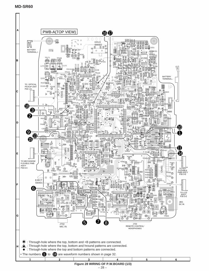
– 28 –
MD-SR60
• The numbers 1 to 18 are waveform numbers shown in page 32.
: Through-hole where the top, bottom and +B patterns are connected. : Through-hole where the top, bottom and hround patterns are connected. : Through-hole where the top and bottom patterns are connected.
A
B
C
D
E
F
G
H
1 2 3 4 5 6
Figure 28 WIRING OF P.W.BOARD (1/3)
R291
HOLDSW402
IC257
R292TP803
TP171 TP106 C291
TP441
C454
R464TP100
L171
C171
C172
CK112
C11
0
C10
9
C11
2
C11
1
C106
C107TP105 TP
144 TP110
TP139
TP
118
TP103
TP101
C161TP
114
R106Q101
CK
105
IC101
C102
CK101 CK107
R154
C10
3
R408
TP109
C10
4
R407
TP111
CN
101 R105
TP
102
TP
116
TP404 CK106
CK104 CK10
2
TP115 C130
CK103 TP151 TP117 R422
TP145
TP108
TP119 CK108
TP
133
TP121
TP130
TP
131
TP132
TP122 TP
120
TP205
R10
1 R102
R103 R104
CK901
TP
351
C121
C122 C123
C124R920 R412
TP
409
TP665 TP407
TP20
1 R411
IC351
R413
C357TP658
R414IC402
TP
408
TP
410
TP
411
R415
TP655 TP659
R416
TP601
R404
R40
6 R405
TP405 TP
652 R403
TP
651
TP406 TP660
TP
653
C604
C603
L604 L603
TP661
C609
R921
TP657
TP610
CN
601
R922
L609
TP654
C836
IC873 IC601
L610
C62
2
TP666 C610
TP662
TP663
TP664
C837
TP602
C651
R600
TP708 EJECTSW401
L710C715
Q711
TP
707
TP706
C734C733
R728R717
C70
4
C731
R70
1 TP202
R718
C505
C50
6
R727
TP702 C703
R703
TP703
C713
TP713
R502
C50
2
IC701
TP
701
TP704
R715
IC501 TP714 C501
R713
R716
TP712 R501
R714
TP705
R72
9
TP
500
C721
TP711
R730 L500
C722 TP727 TP728 TP729
TP721 L800TP722
TP805
D801
TP772
TP
725
TP726
TP723
R492
TP801
TP802 C492
TP771 IC703
R7
65
D49
4R762 C491
TP724
R766
D49
5
D496
L801
R808R810
C765 C766
C758D492 L491
C481
C76
0R
757
R75
8
R75
4
R761
TP453
R457
TP412 TP451
TP452
R456
TP481
TP454
R458
R455
TP482
TP456
C482
CN
482
CN
451
TP483 TP460
TP486
TP458
TP461 TP487
TP489 TP463
TP459 TP488
R451
R452R
453
R454
TP462
TP206
TP656 R463
TP457
R806
TP455 TP419
R465
D80
3
TP210
R461
Q891
TP209
R466
R811TP41
7 R802D431
TP416 TP208
D802 R801
R809
R803C431
TP204
R431IC431
R853 IC852 TP403
TP400 IC401 C857
C860C856
R854TP401 C825
XL401
R85
5
R856R402 D822TP414 C830
R831
TP413 C876
R823 C828
IC822 C401 R832TP415 TP212
R871C839
C82
7
TP203 TP402
C82
6
IC87
1
R826R443R423
R425
R424
C206
TP207 D823
C259TP804
C200TP200
R287
R269
R283
R819
R277IC809
R26
1R
262
R263
R266R267
TP809
Q257
R284IC259
R279R271
R2
70
C2
55 IC256 IC258
IC2
53
IC26
0 TP
842
R28
8
R281
R286
C254
R250
R272
R256
R255R257
R28
5
R2
82
Q251D281 R252
IC255
IC251 R253
R251
R293
Q250
TP
841 D251
C25
1
C25
3R
254
C252
R29
5R
294R296
IC89
2
R827R824
R825
R857
D461
C714
1
5
1015
20
2530 35 40 45
50
55
60
65
70
80859095
PWB-A(TOP VIEW)
1
4 5
858
14
11
1
1
1
1
1
1
1
33
3
3
3
44
4
4
4
4
4
4
6
6
6
6
1 3
4
6
1 34
6
5
5
5
8
8
3
2
100
75
76
26
1
2 3
J801DC IN
J703REMOTE CONTROL/
HEADPHONES
1
1
2
3
3
4
1
1
1
5
5
1012
1
510
12
1315 20
24 13
15 20
24
8
9
1015
16
8 7
21
653
4
13
1
9
1
1
5
10121520
132425
30
35
3640
3745
48
1
5
10
1215 20
13 2425
30
35
3640
37
45
48
1
22
7
5
51
1
4
8
8
10
14
1
164 5TO MECHANISM
FLEXIBLE PWBASS'YP30 6-C
TO OPTICALPICKUP UNITP30 1-D
BATTERYTERMINAL,+
BATTERYTERMINAL,-
51
6
34
23
913
15
18
5 7 8
6
1
1411
10
TO LCDASS'Y
P30 5-E
TO KEYFLEXIBLE
PWB ASS'YP30 3-E
1716
3
4
2
J702MIC IN
L451L452
L453L454
L456
L711
L712
L714
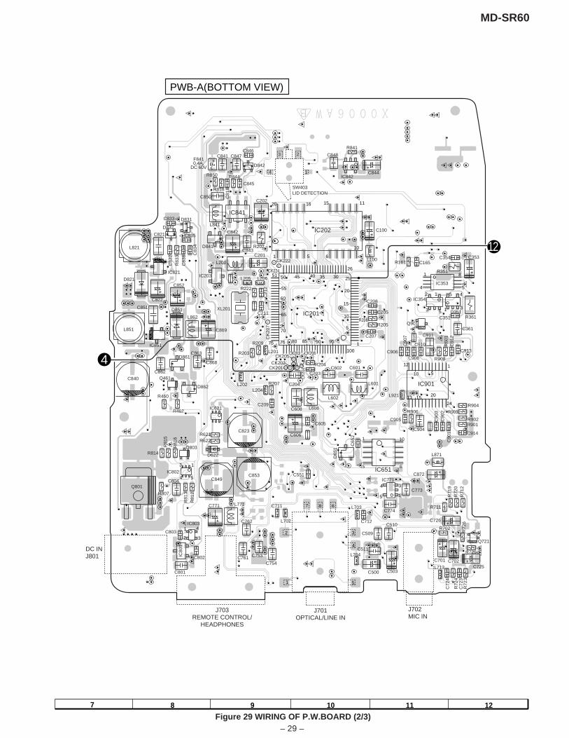
– 29 –
MD-SR60
7 8 9 10 11 12
Figure 29 WIRING OF P.W.BOARD (2/3)
R72
3C
723
R72
4
C72
4
J702MIC IN
L704
C503C500
J701OPTICAL/LINE IN
C725C702C701
C511R725
R72
6C510
C509
Q721
R702
C712
L703
C726
R711
R71
2R
720
R71
9
C774
C773
IC771 C551 C872
L871
10
10
65
5
1
1
D65
1
IC651
C65
2
C90
1C
902
C90
3C914
C605C904
R906
C905R901R902
R903C608 L608 R904
IC901
CK203 CK206
C203
R204
C91
2R
601
R908
C910
C908
C90
7
C906 C913
C911C361
C207
R205 Q901
IC201 R206 C351 R361
IC354
C205 D351
C208
IC353
C353C165R161
R351
L100 C354
C100IC202
IC842
C848
C844
R841C846
C847C841F8410.4A,
DC 60V D842
SW403LID DETECTION
R850
C845
R844
C81
8R818
C850
4 1
23
C202
L841C833
IC841 D831
C835
D832
R202D841C843
C842C821
L821
C83
4
C83
8
R83
3
C83
2 C201
L200
IC821
CK222
IC203 CK224
D821
C822
C21
2R222C852
C211XL201 C851
CK
207
D851
L851
L862
C869
IC851
C868
C863CK205 D861
C862
CK20
4
CK202 CK201
C840 Q461
D862
C209R462
R460
IC621
C606R621C823
R622
D622
R81
6
R81
5
R814Q803
C853IC802
C849
R807
R81
2R
813
C804Q801
L702
C711L771C771
IC803 C762
C803
IC80
1
DC INJ801 C753C761C802
C754
C801
J703REMOTE CONTROL/
HEADPHONES
C204
C602 C601
L602
L601
20 16 15 11
1 5 6
10
13
4 5
12
13 15 20
24
1
100
1
34
5
1
14
2
3 35 1
45
5
8
5
10
15
20
25303540455051
55
60
65
70
75 76 80 85 90 95
26
7
22
1
1
5
4
43
3
12
4
PWB-A(BOTTOM VIEW)
8 6
L204L202
L201
L205 L206
L921
R207
R203
R209
L713
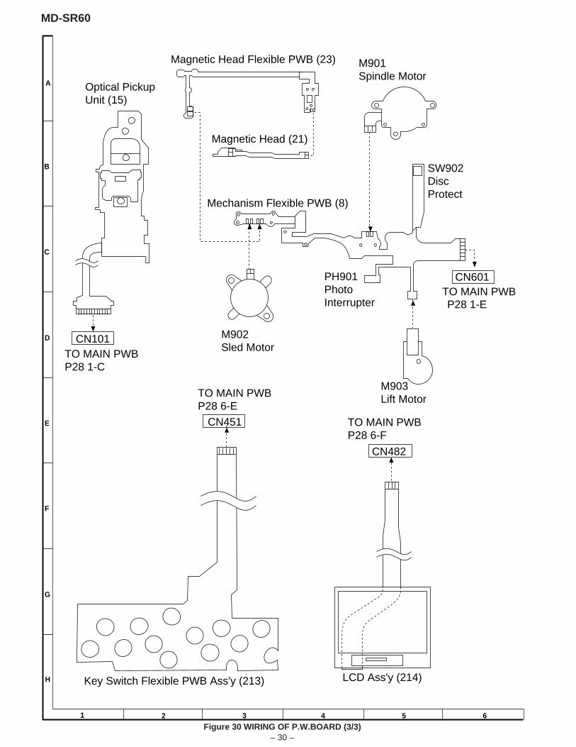
– 30 –
MD-SR60
Figure 30 WIRING OF P.W.BOARD (3/3)
A
B
C
D
E
F
G
H
1 2 3 4 5 6
Optical Pickup Unit (15)
Magnetic Head Flexible PWB (23)
Magnetic Head (21)
Mechanism Flexible PWB (8)
M902Sled Motor
PH901PhotoInterrupter
M901Spindle Motor
SW902DiscProtect
TO MAIN PWBCN601
TO MAIN PWBP28 6-F
CN482
LCD Ass'y (214)Key Switch Flexible PWB Ass'y (213)
CN451
CN101TO MAIN PWBP28 1-C
P28 1-E
TO MAIN PWBP28 6-E
M903Lift Motor
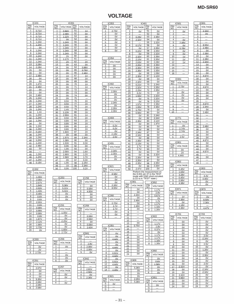
– 31 –
MD-SR60
VOLTAGE
PIN NO. VOLTAGE PIN
NO. VOLTAGE
IC401PIN NO. VOLTAGE
PIN NO. VOLTAGE PIN
NO. VOLTAGE
PIN NO. VOLTAGE
1
PIN NO. VOLTAGE
PIN NO. VOLTAGE
PIN NO. VOLTAGE
PIN NO. VOLTAGE
PIN NO. VOLTAGE
PIN NO. VOLTAGE
PIN NO. VOLTAGE
PIN NO. VOLTAGE
PIN NO. VOLTAGE
PIN NO. VOLTAGE
Preform the measurement on the IC401 pin 37 in the TEST mode with GND short-circuited.(LCD is in "TEST" state.)
PIN NO. VOLTAGE
IC501
IC701 IC822
IC841
IC402
IC871
IC354
IC353 IC601
IC651
IC703
IC771
IC801
IC802
IC901
100
1 2
456789
1011121314151617181920212223242526272829303132333435363738394041424344454647484950
51525354555657585960616263646566676869707172737475767778798081828384858687888990919293949596979899
3
1 2
456789
101112131415
3
1 2
456789
101112131415161718192021222324
3
2
45
3
1 2
45678
3
1 2
45678
3
1 2
45
3
1 2
45
3
910
1 2
45
3
1 2
45678
3
1 23
1 2
45678
3
1 2
456789
1011121314151617181920
3
1 2
456789
101112131415161718192021222324252627282930313233343536
3
1 2
456789
101112131415161718192021222324
3
1 2
456
3
PIN NO. VOLTAGE
IC431
1 2
43
PIN NO. VOLTAGE
IC803
1 2
43
PIN NO. VOLTAGE
IC809
1 2
456
3
PIN NO. VOLTAGE
IC892
1 2
456
3
2.73V0V0V0V0V0V0V0V
0V0V0V0V0V
2.35V0V0V0V
2.34V0V
2.35V2.35V
PIN NO. VOLTAGE
IC404
1 2
45
3
0.2V0.2V
0V2.19V2.5V
2.34V2.35V
0V0V
0V—
0.29V2.32V
— 0.17V
0V0.22V
0V2.32V2.15V2.03V2.25V2.35V2.35V
0V2.35V
0V2.32V0.21V2.32V2.25V0.2V
1.55V0V0V
1.57V1.05V1.75V0.56V
0V0V
2.35V0V0V0V
2.34V2.34V
0V2.35V2.13V2.7V2.7V
0V0V
2.35V2.35V2.35V
0V2.47V
0V0V
2.35V0V
2.32V0V
2.35V2.35V2.32V2.35V2.35V2.28V2.35V2.35V2.35V1.09V1.12V
0V0V
2.34V2.35V2.35V
2V2.32V2.32V0.15V2.35V2.35V
0V0V
2.34V2.34V2.12V1.47V
0V0V0V0V0V0V0V0V0V0V
2.32V0V0V
2.35V2.33V
0V
0V— — 0V
2.49V0V
0.78V0V0V1V1V1V— — — — 16
PIN NO. VOLTAGE
IC621
1 2
456
3
8.58V0V0V0V
2.34V8.55V
2.73V— 0V0V0V0V— — — —
373839404142434445464748
2.34V0V — — —
8.55V2.48V
0V2.38V
0V2.38V2.34V
0V0V0V0V
4.67V0V0V0V
4.67V0V0V0V0V
— 4.67V2.34V
0V2.48V
— — — —
2.48V0V0V0V0V
4.67V0V0V0V
4.67V — 0V— —
0V0V0V0V0V0V0V0V0V0V0V0V0V0V0V0V
-2.32V0V0V
2.42V0.86V
0V0V0V
0V0V0V0V0V
2.5V-2.34V
0V2.5V
0V1.26V
0V2.35V
0V0V
2.5V0V
-2.34V-2.34V
0V0V0V0V0V
0V2.74V2.74V
— 2.5V
0V2V
4.44V
0.45V1.03V3.28V0.45V0.99V4.38V
4.4V4.46V
0V0V
5.36V0V0V0V
2.35V5.36V
1.17V2.8V
0.37V0V
1.17V1.17V1.16V1.26V
— 2.8V
2.06V2.06V
0V
PIN NO. VOLTAGE
1
IC842
2
45
3
— 2.81V2.56V
0V2.36V
PIN NO. VOLTAGE
IC852
1 2
45678
3
1.17V2.8V
0.67V0V
1.2V1.17V1.16V1.26V
1V2.36V
0V1.18V2.36V
PIN NO. VOLTAGE
IC873
1 2
45
3
0V8.59V2.36V
— 4.47V
0V0.6V
1.58V0V0V0V
0V0V
2.34V0V
2.49V0V
2.49V0V— — — — 0V
0.75V— — — 0V0V0V0V0V0V0V
21222324
PIN NO. VOLTAGE PIN
NO. VOLTAGE
IC201
100
1 2
456789
1011121314151617181920212223242526272829303132333435363738394041424344454647484950
51525354555657585960616263646566676869707172737475767778798081828384858687888990919293949596979899
3
0.84V2.48V1.22V
0V1.24V1.24V1.24V1.24V1.24V
2V1.17V
2V0V0V0V0V1V0V0V0V0V0V0V0V0V
0.5V0.5V0.5V1.4V
1.13V2.55V0.5V0.8V0.8V0.8V0.8V
1.84V0V
1.97V1.38V1.53V0.9V1.9V
2.56V1.66V1.56V
0V1.9V
1V0.9V
PIN NO. VOLTAGE
IC101
1 2
456789
101112131415161718192021222324252627282930313233343536
3
373839404142434445464748
0.71V0.71V0.71V0.71V1.24V1.24V
0V1.24V1.24V1.24V1.24V1.24V2.28V2.28V
0V0V
2.48V0V0V
1.47V2.35V
0V0V
2.48V1.24V1.24V1.24V1.24V1.24V1.2V
1.24V1.24V1.24V
0V1.24V1.24V0.16V1.24V1.24V1.24V1.24V2.48V
0V —
1.24V1.24V1.24V0.19V
1V0V0V0V0V2V0V0V0V0V
— 2V0V
0.88V0.76V2.46V
1V2V0V1V1V0V0V0V
—2V2V2V0V2V1V2V2V2V1V2V2V0V
2.34V0V
0.3V0V0V
1.6V1.2V1.7V0.3V
2.25V2.34V0.2V
PIN NO. VOLTAGE
IC202
1 2
456789
1011121314151617181920
3
1.55V2.05V2.57V1.94V0.93V1.43V0.49V0.6V0.6V
2.55V0.6V
0.99V0.99V0.99V0.8V
1.87V2.12V1.66V1.73V
0V
PIN NO. VOLTAGE
IC203
1 23
0V2V
2.73V
PIN NO. VOLTAGE
IC251
1 2
45678
3
2.07V0V0V0V
5.35V2.08V2.08V2.08V
PIN NO. VOLTAGE
IC253
1 2
456
3
5.36V5.31V5.31V
0V0V0V
PIN NO. VOLTAGE
IC255
1 2
45678
3
-1.05V0V0V
-2.25V0V0V
-1.65V2.72V
PIN NO. VOLTAGE
IC256
1 2
456
3
0V — —
0V0V0V
PIN NO. VOLTAGE
IC257
1 2
43
0V0V
— 0V
PIN NO. VOLTAGE
IC258
1 2
456
3
0V0.59V4.93V
0V0V0V
PIN NO. VOLTAGE
IC260
1 2
456
3
2.72V2.7V2.7V
0V0V—
PIN NO. VOLTAGE
IC259
1 2
456
3
— 0.56V0.56V
0V0.56V2.63V PIN
NO. VOLTAGE
IC351
1 2
456789
1011121314
3
0V0V
4.44V0V0V
4.44V0V
0.91V4.44V
0V0.91V4.44V
0V4.49V
PIN NO. VOLTAGE
IC821
S GD
PIN NO. VOLTAGE
IC851
S GD
0V— —
0V— —
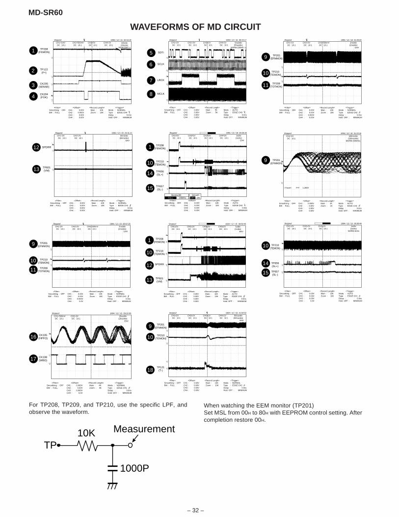
– 32 –
MD-SR60
WAVEFORMS OF MD CIRCUIT1994 / 12 / 15 22:54:19
=Filter= =Offset= =Record Length=Smoothiing : OFFBW : FULL
CH1 : 0.00VCH2 : 0.000V
Main : 10KZoom : 10K
CH3 : 0.00VCH4 : 0.00V
=Trigger=Mode : NORMALType : EDGE CH4Detay : 0.0nsHold OFF : MINIMUM
T
TP208(FEMON)
CK204(FOK)
TP122(F+)
CK205(SENSE)
StoppedCH1=1mVDC 10:1
CH3=5VDC 10:1
CH4=2VDC 10:1
50ms/div(50ms/div)
NORM:200kS / s
CH2=500mVDC 10:1
T
1
4
3
2
1
2
3
4
NORM:100MS / s
1994 / 12 / 16 00:24:17
=Filter= =Offset= =Record Length=Smoothiing : OFFBW : FULL
CH1 : 0.00VCH2 : 0.00V
Main : 5KZoom : 5K
CH3 : 0.00VCH4 : 0.00V
=Trigger=Mode : AUTOType : EDGE CH3Detay : 0.0nsHold OFF : MINIMUM
T
SDTi
MCLK
SCLK
LRCK
StoppedCH1=2VDC 10:1
CH3=2VDC 10:1
CH4=2VDC 10:1 (50us/div)
50us/divCH2=2VDC 10:1
T
1
4
3
2
5
6
7
8
ENV
1994 / 12 / 16 01:03:40
=Filter= =Offset= =Record Length=Smoothiing : OFFBW : FULL
CH1 : 0.00VCH2 : 0.00V
Main : 10KZoom : 10K
CH3 : 0.000VCH4 : 0.00V
=Trigger=Mode : NORMALType : EDGE CH2Detay : 0.0nsHold OFF : MINIMUM
T
TP201(EFMMON)
TP210(TEMON)
TP209(TOTMON)
StoppedCH1=1VDC 10:1
CH3=500mVDC 10:1 (2ms/div)
2ms/divCH2=2VDC 10:1
T
1
2
9
10
11
ENV
1994 / 12 / 15 23:31:21
=Filter= =Offset= =Record Length=Smoothiing : OFFBW : FULL
CH1 : 0.00VCH2 : 0.00V
Main : 10KZoom : 10K
CH3 : 0.00VCH4 : 0.00V
=Trigger=Mode : NORMALType : EDGE CH1Detay : 0.0nsHold OFF : MINIMUM
T
SPDRR
TP601(VM)
StoppedCH1=2VDC 10:1 (50ms/div)
50ms/divCH2=2VDC 10:1
T
1
2
12
13
FULL 20MHzBandwidth
ONSmooth
OFF
1994 / 12 / 18 09:26:46
=Filter= =Offset= =Record Length=Smoothiing : OFFBW : FULL
CH1 : 0.00VCH2 : 0.00V
Main : 10KZoom : 10K
CH3 : 0.00VCH4 : 0.00V
=Trigger=Mode : AUTOType : EDGE CH2Detay : 0.0nsHold OFF : MINIMUM
T
TP208(FEMON)
TP210(TEMON)
TP656(SL+)
TP657(SL-)
StoppedCH1=2VDC 10:1
CH3=2VDC 10:1
CH4=2VDC 10:1 (1s/div)
1s/divCH2=2VDC 10:1
1
4
3
2
ENV
1
10
14
15
1994 / 12 / 16 01:23:16
=Filter=
=Tracel= P-P 1.280V
=Offset= =Record Length=Smoothiing : OFFBW : FULL
CH1 : 0.000VCH2 : 0.00V
Main : 1KZoom : 1K
CH3 : 0.00VCH4 : 0.00V
=Trigger=Mode : AUTOType : EDGE CH1Detay : 0.0nsHold OFF : MINIMUM
TTP201(EFMMON)
StoppedCH1=2VDC 10:1 (500ms/div)
500ms/div
1
MORM:200MS/s
9
1994 / 12 / 15 08:57:26
=Filter= =Offset= =Record Length=Smoothiing : OFFBW : FULL
CH1 : 0.00VCH2 : 0.00V
Main : 10KZoom : 10K
CH3 : 0.000VCH4 : 0.0V
=Trigger=Mode : NORMALType : EDGE CH1Detay : 0.0nsHold OFF : MINIMUM
T
TP201(EFMMON)
TP210(TEMON)
TP209(TOTMON)
StoppedCH1=2VDC 10:1 (2ms/div)
2ms/divCH2=2VDC 10:1
1
2
ENV
T
CH3=500mVDC 10:1
9
10
11
1994 / 12 / 15 09:58:45
=Filter= =Offset= =Record Length=Smoothiing : OFFBW : FULL
CH1 : 0.00VCH2 : 0.00V
Main : 10KZoom : 10K
CH3 : 0.00VCH4 : 0.00V
=Trigger=Mode : AUTOType : EDGE CH1Detay : 0.0nsHold OFF : MINIMUM
T
TP208(FEMON)
TP210(TEMON)
SPDRR
TP601(VM)
StoppedCH1=2VDC 10:1
CH3=2VDC 10:1
CH4=2VDC 10:1 (1s/div)
1s/divCH2=2VDC 10:1
1
3
4
2
ENV
1
10
12
13
1994 / 12 / 15 08:39:46
=Filter= =Offset= =Record Length=Smoothiing : OFFBW : FULL
CH1 : 0.00VCH2 : 0.00V
Main : 10KZoom : 10K
CH3 : 0.00VCH4 : 0.0V
=Trigger=Mode : AUTOType : EDGE CH1Detay : 0.0nsHold OFF : MINIMUM
T
TP210(TEMON)
TP656(SL+)
TP657(SL-)
StoppedCH1=2VDC 10:1
CH3=2VDC 10:1 (1s/div)
1s/divCH2=2VDC 10:1
1
3
2
NORM:1kS/s
10
14
15
1994 / 12 / 15 21:54:52
=Filter= =Offset= =Record Length=Smoothiing : OFFBW : FULL
CH1 : 0.00VCH2 : 0.00V
Main : 10KZoom : 10K
CH3 : 0.00VCH4 : 0.00V
=Trigger=Mode : NORMALType : EDGE CH2Detay : 0.0nsHold OFF : MINIMUM
T
T
TP201(EFMMON)
TP210(TEMON)
TP121(T-)
StoppedCH1=2VDC 10:1
CH3=1VDC 10:1
CH4=1VDC 10:1 (500us/div)
500us/divCH2=2VDC 10:1
1
3
4
2
ENV
9
10
18
For TP208, TP209, and TP210, use the specific LPF, andobserve the waveform.
When watching the EEM monitor (TP201)Set MSL from 00H to 80H with EEPROM control setting. Aftercompletion restore 00H.
1994 / 12 / 15 09:10:03
=Filter= =Offset= =Record Length=Smoothiing : OFFBW : FULL
CH1 : 0.000VCH2 : 0.00V
Main : 4KZoom : 4K
CH3 : 0.000VCH4 : 0.0V
=Trigger=Mode : NORMALType : EDGE CH1Detay : 0.0nsHold OFF : MINIMUM
T
CK105(HPFO)
CK108(WBO)
StoppedCH1=500mVDC 10:1 (20us/div)
20us/divCH2=2VDC 10:1
1
2
ENV
16
17
1000P
10KTP
Measurement
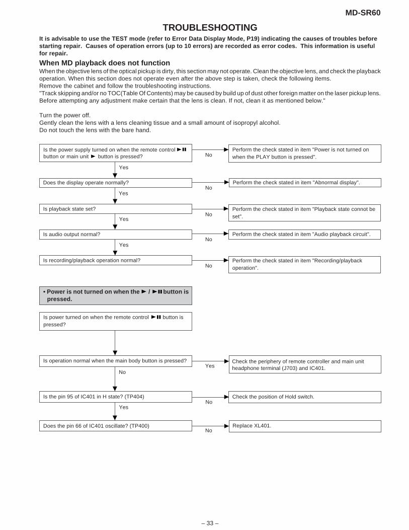
– 33 –
MD-SR60
TROUBLESHOOTINGIt is advisable to use the TEST mode (refer to Error Data Display Mode, P19) indicating the causes of troubles beforestarting repair. Causes of operation errors (up to 10 errors) are recorded as error codes. This information is usefulfor repair.
When MD playback does not functionWhen the objective lens of the optical pickup is dirty, this section may not operate. Clean the objective lens, and check the playbackoperation. When this section does not operate even after the above step is taken, check the following items.Remove the cabinet and follow the troubleshooting instructions."Track skipping and/or no TOC(Table Of Contents) may be caused by build up of dust other foreign matter on the laser pickup lens.Before attempting any adjustment make certain that the lens is clean. If not, clean it as mentioned below."
Turn the power off.Gently clean the lens with a lens cleaning tissue and a small amount of isopropyl alcohol.Do not touch the lens with the bare hand.
Is the power supply turned on when the remote controlbutton or main unit button is pressed? No
Perform the check stated in item "Power is not turned onwhen the PLAY button is pressed".
Perform the check stated in item "Abnormal display".No
Yes
Does the display operate normally?
Is playback state set?
Yes
Perform the check stated in item "Playback state connot beset".No
Is audio output normal?
Yes
Perform the check stated in item "Audio playback circuit".No
Is recording/playback operation normal?
Yes
Perform the check stated in item "Recording/playbackoperation".No
• Power is not turned on when the / button ispressed.
NoYes
Check the periphery of remote controller and main unitheadphone terminal (J703) and IC401.
NoIs the pin 95 of IC401 in H state? (TP404)
Is operation normal when the main body button is pressed?
Check the position of Hold switch.
Is power turned on when the remote control button ispressed?
NoDoes the pin 66 of IC401 oscillate? (TP400) Replace XL401.
Yes
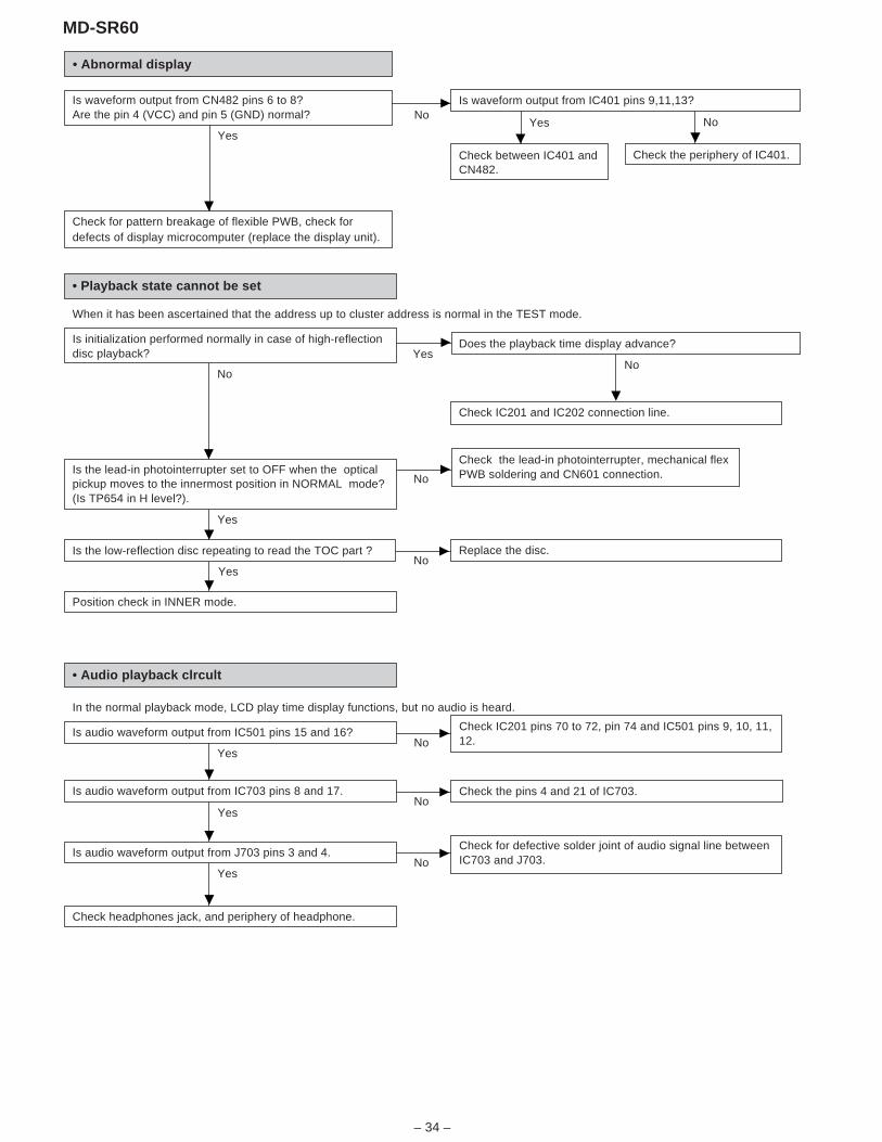
– 34 –
MD-SR60
Yes
Check for defective solder joint of audio signal line betweenIC703 and J703.No
Yes
Is audio waveform output from J703 pins 3 and 4.
Check the pins 4 and 21 of IC703.No
Yes
Is audio waveform output from IC703 pins 8 and 17.
Check IC201 pins 70 to 72, pin 74 and IC501 pins 9, 10, 11,12.No
• Abnormal display
No
Yes
Are the pin 4 (VCC) and pin 5 (GND) normal?Is waveform output from IC401 pins 9,11,13?Is waveform output from CN482 pins 6 to 8?
• Playback state cannot be set
Is initialization performed normally in case of high-reflectiondisc playback?
Yes
Check between IC401 andCN482.
No
Check the periphery of IC401.
Does the playback time display advance?Yes
Position check in INNER mode.
Check IC201 and IC202 connection line.
Is the lead-in photointerrupter set to OFF when the opticalpickup moves to the innermost position in NORMAL mode?(Is TP654 in H level?).
Check the lead-in photointerrupter, mechanical flexPWB soldering and CN601 connection.No
Is the low-reflection disc repeating to read the TOC part ?
Yes
NoNo
Replace the disc.No
• Audio playback clrcult
When it has been ascertained that the address up to cluster address is normal in the TEST mode.
Yes
Is audio waveform output from IC501 pins 15 and 16?
Check headphones jack, and periphery of headphone.
In the normal playback mode, LCD play time display functions, but no audio is heard.
Check for pattern breakage of flexible PWB, check fordefects of display microcomputer (replace the display unit).
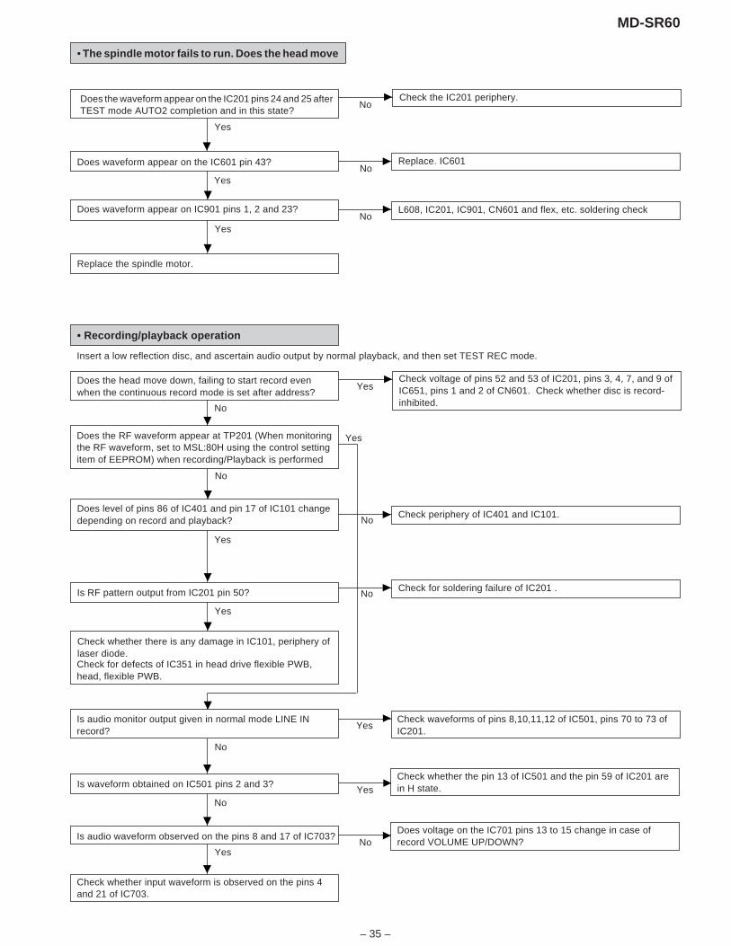
– 35 –
MD-SR60
• The spindle motor fails to run. Does the head move
NoDoes the waveform appear on the IC201 pins 24 and 25 afterTEST mode AUTO2 completion and in this state?
Check the IC201 periphery.
Yes
Does waveform appear on the IC601 pin 43?
Does waveform appear on IC901 pins 1, 2 and 23?
Replace the spindle motor.
YesNo
L608, IC201, IC901, CN601 and flex, etc. soldering check
NoReplace. IC601
Yes
• Recording/playback operation
Insert a low reflection disc, and ascertain audio output by normal playback, and then set TEST REC mode.
YesDoes the head move down, failing to start record evenwhen the continuous record mode is set after address?
No
Does level of pins 86 of IC401 and pin 17 of IC101 changedepending on record and playback?
Is RF pattern output from IC201 pin 50?
Yes
NoCheck for soldering failure of IC201 .
NoCheck periphery of IC401 and IC101.
Check whether there is any damage in IC101, periphery oflaser diode.
Yes
Check for defects of IC351 in head drive flexible PWB,head, flexible PWB.
No
YesIs audio monitor output given in normal mode LINE INrecord?
Check waveforms of pins 8,10,11,12 of IC501, pins 70 to 73 ofIC201.
Is waveform obtained on IC501 pins 2 and 3?
No
YesCheck whether the pin 13 of IC501 and the pin 59 of IC201 arein H state.
No
NoDoes voltage on the IC701 pins 13 to 15 change in case ofrecord VOLUME UP/DOWN?
Is audio waveform observed on the pins 8 and 17 of IC703?
Yes
Check whether input waveform is observed on the pins 4and 21 of IC703.
Yes
Check voltage of pins 52 and 53 of IC201, pins 3, 4, 7, and 9 ofIC651, pins 1 and 2 of CN601. Check whether disc is record-inhibited.
Does the RF waveform appear at TP201 (When monitoringthe RF waveform, set to MSL:80H using the control settingitem of EEPROM) when recording/Playback is performed
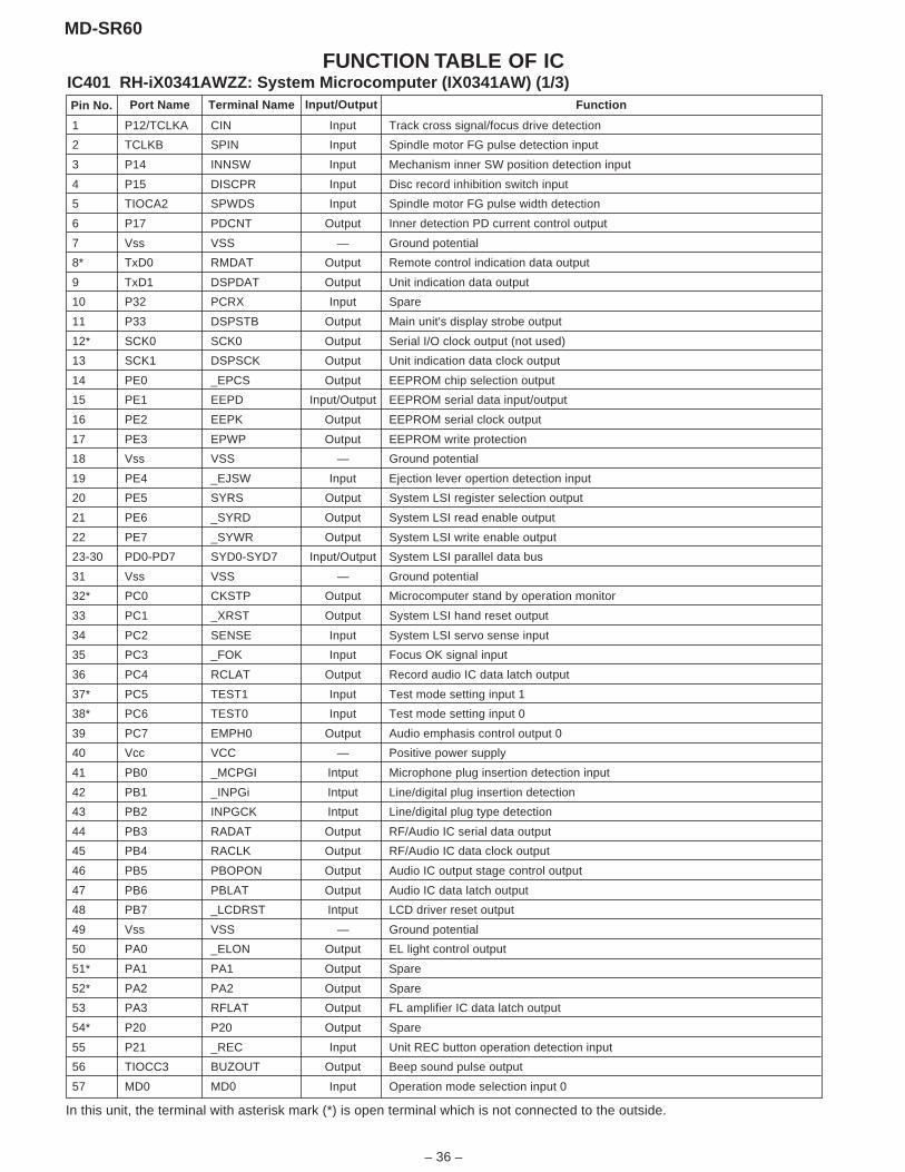
– 36 –
MD-SR60
1 P12/TCLKA CIN Input Track cross signal/focus drive detection
2 TCLKB SPIN Input Spindle motor FG pulse detection input
3 P14 INNSW Input Mechanism inner SW position detection input
4 P15 DISCPR Input Disc record inhibition switch input
5 TIOCA2 SPWDS Input Spindle motor FG pulse width detection
6 P17 PDCNT Output Inner detection PD current control output
7 Vss VSS — Ground potential
8* TxD0 RMDAT Output Remote control indication data output
9 TxD1 DSPDAT Output Unit indication data output
10 P32 PCRX Input Spare
11 P33 DSPSTB Output Main unit's display strobe output
12* SCK0 SCK0 Output Serial I/O clock output (not used)
13 SCK1 DSPSCK Output Unit indication data clock output
14 PE0 _EPCS Output EEPROM chip selection output
15 PE1 EEPD Input/Output EEPROM serial data input/output
16 PE2 EEPK Output EEPROM serial clock output
17 PE3 EPWP Output EEPROM write protection
18 Vss VSS — Ground potential
19 PE4 _EJSW Input Ejection lever opertion detection input
20 PE5 SYRS Output System LSI register selection output
21 PE6 _SYRD Output System LSI read enable output
22 PE7 _SYWR Output System LSI write enable output
23-30 PD0-PD7 SYD0-SYD7 Input/Output System LSI parallel data bus
31 Vss VSS — Ground potential
32* PC0 CKSTP Output Microcomputer stand by operation monitor
33 PC1 _XRST Output System LSI hand reset output
34 PC2 SENSE Input System LSI servo sense input
35 PC3 _FOK Input Focus OK signal input
36 PC4 RCLAT Output Record audio IC data latch output
37* PC5 TEST1 Input Test mode setting input 1
38* PC6 TEST0 Input Test mode setting input 0
39 PC7 EMPH0 Output Audio emphasis control output 0
40 Vcc VCC — Positive power supply
41 PB0 _MCPGI Intput Microphone plug insertion detection input
42 PB1 _INPGi Intput Line/digital plug insertion detection
43 PB2 INPGCK Intput Line/digital plug type detection
44 PB3 RADAT Output RF/Audio IC serial data output
45 PB4 RACLK Output RF/Audio IC data clock output
46 PB5 PBOPON Output Audio IC output stage control output
47 PB6 PBLAT Output Audio IC data latch output
48 PB7 _LCDRST Intput LCD driver reset output
49 Vss VSS — Ground potential
50 PA0 _ELON Output EL light control output
51* PA1 PA1 Output Spare
52* PA2 PA2 Output Spare
53 PA3 RFLAT Output FL amplifier IC data latch output
54* P20 P20 Output Spare
55 P21 _REC Input Unit REC button operation detection input
56 TIOCC3 BUZOUT Output Beep sound pulse output
57 MD0 MD0 Input Operation mode selection input 0
IC401 RH-iX0341AWZZ: System Microcomputer (IX0341AW) (1/3)FUNCTION TABLE OF IC
Pin No. FunctionPort Name Terminal Name Input/Output
In this unit, the terminal with asterisk mark (*) is open terminal which is not connected to the outside.
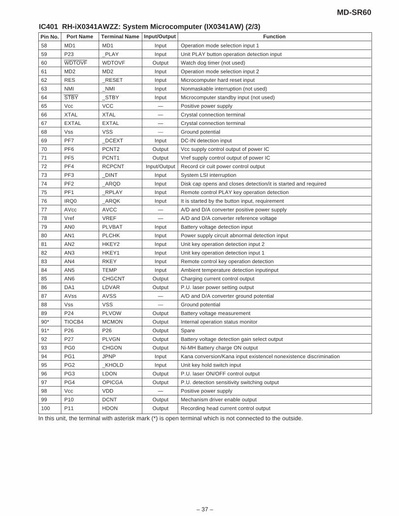
– 37 –
MD-SR60
58 MD1 MD1 Input Operation mode selection input 1
59 P23 _PLAY Input Unit PLAY button operation detection input
60 WDTOVF WDTOVF Output Watch dog timer (not used)
61 MD2 MD2 Input Operation mode selection input 2
62 RES _RESET Input Microcomputer hard reset input
63 NMI _NMI Input Nonmaskable interruption (not used)
64 STBY _STBY Input Microcomputer standby input (not used)
65 Vcc VCC — Positive power supply
66 XTAL XTAL — Crystal connection terminal
67 EXTAL EXTAL — Crystal connection terminal
68 Vss VSS — Ground potential
69 PF7 _DCEXT Input DC-IN detection input
70 PF6 PCNT2 Output Vcc supply control output of power IC
71 PF5 PCNT1 Output Vref supply control output of power IC
72 PF4 RCPCNT Input/Output Record cir cuit power control output
73 PF3 _DINT Input System LSI interruption
74 PF2 _ARQD Input Disk cap opens and closes detection/it is started and required
75 PF1 _RPLAY Input Remote control PLAY key operation detection
76 IRQ0 _ARQK Input It is started by the button input, requirement
77 AVcc AVCC — A/D and D/A converter positive power supply
78 Vref VREF — A/D and D/A converter reference voltage
79 AN0 PLVBAT Input Battery voltage detection input
80 AN1 PLCHK Input Power supply circuit abnormal detection input
81 AN2 HKEY2 Input Unit key operation detection input 2
82 AN3 HKEY1 Input Unit key operation detection input 1
83 AN4 RKEY Input Remote control key operation detection
84 AN5 TEMP Input Ambient temperature detection inputinput
85 AN6 CHGCNT Output Charging current control output
86 DA1 LDVAR Output P.U. laser power setting output
87 AVss AVSS — A/D and D/A converter ground potential
88 Vss VSS — Ground potential
89 P24 PLVOW Output Battery voltage measurement
90* TIOCB4 MCMON Output Internal operation status monitor
91* P26 P26 Output Spare
92 P27 PLVGN Output Battery voltage detection gain select output
93 PG0 CHGON Output Ni-MH Battery charge ON output
94 PG1 JPNP Input Kana conversion/Kana input existencel nonexistence discrimination
95 PG2 _KHOLD Input Unit key hold switch input
96 PG3 LDON Output P.U. laser ON/OFF control output
97 PG4 OPICGA Output P.U. detection sensitivity switching output
98 Vcc VDD — Positive power supply
99 P10 DCNT Output Mechanism driver enable output
100 P11 HDON Output Recording head current control output
IC401 RH-iX0341AWZZ: System Microcomputer (IX0341AW) (2/3)Pin No. FunctionPort Name Terminal Name Input/Output
In this unit, the terminal with asterisk mark (*) is open terminal which is not connected to the outside.
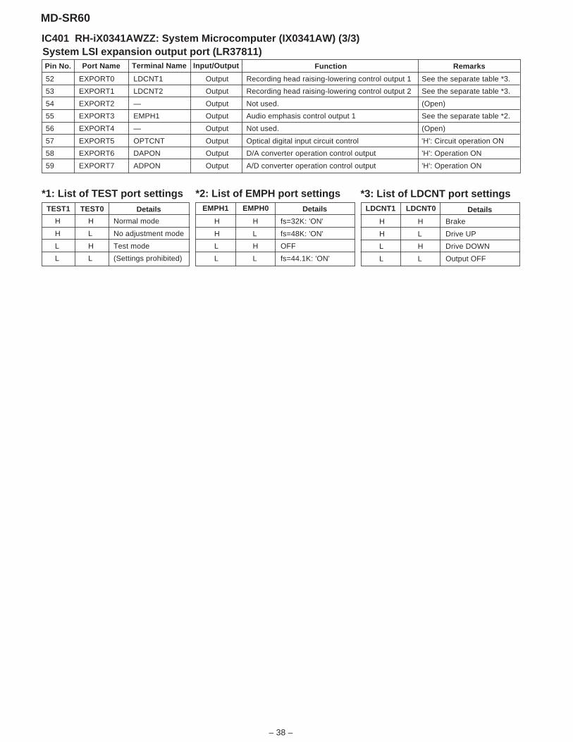
– 38 –
MD-SR60
52 EXPORT0 LDCNT1 Output Recording head raising-lowering control output 1 See the separate table *3.
53 EXPORT1 LDCNT2 Output Recording head raising-lowering control output 2 See the separate table *3.
54 EXPORT2 — Output Not used. (Open)
55 EXPORT3 EMPH1 Output Audio emphasis control output 1 See the separate table *2.
56 EXPORT4 — Output Not used. (Open)
57 EXPORT5 OPTCNT Output Optical digital input circuit control 'H': Circuit operation ON
58 EXPORT6 DAPON Output D/A converter operation control output 'H': Operation ON
59 EXPORT7 ADPON Output A/D converter operation control output 'H': Operation ON
System LSI expansion output port (LR37811)Pin No. FunctionPort Name Terminal Name Input/Output Remarks
H H Normal mode
H L No adjustment mode
L H Test mode
L L (Settings prohibited)
TEST1 Details
*1: List of TEST port settings
H H fs=32K: 'ON'
H L fs=48K: 'ON'
L H OFF
L L fs=44.1K: 'ON'
EMPH1 EMPH0 Details
*2: List of EMPH port settings
H H Brake
H L Drive UP
L H Drive DOWN
L L Output OFF
LDCNT1 LDCNT0 Details
*3: List of LDCNT port settingsTEST0
IC401 RH-iX0341AWZZ: System Microcomputer (IX0341AW) (3/3)
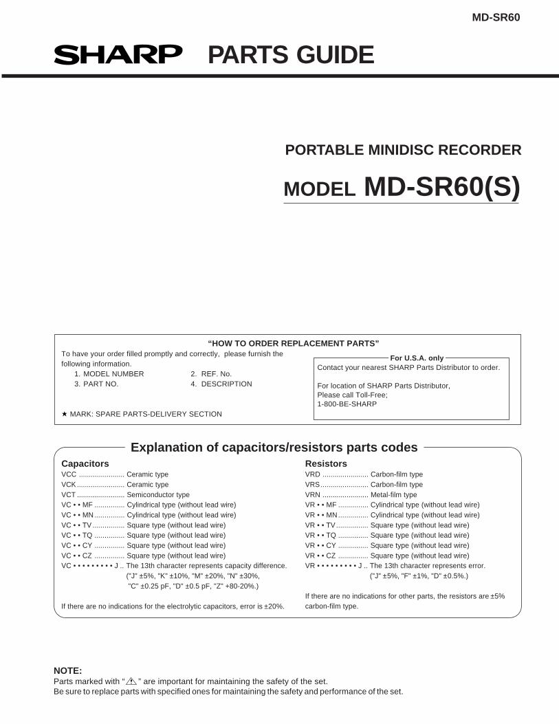
MD-SR60
PARTS GUIDE
NOTE:Parts marked with “ ” are important for maintaining the safety of the set.Be sure to replace parts with specified ones for maintaining the safety and performance of the set.
“HOW TO ORDER REPLACEMENT PARTS”To have your order filled promptly and correctly, please furnish thefollowing information.
1. MODEL NUMBER 2. REF. No.3. PART NO. 4. DESCRIPTION
MARK: SPARE PARTS-DELIVERY SECTION
For U.S.A. onlyContact your nearest SHARP Parts Distributor to order.
For location of SHARP Parts Distributor,Please call Toll-Free;1-800-BE-SHARP
Explanation of capacitors/resistors parts codesCapacitorsVCC ....................... Ceramic typeVCK ........................ Ceramic typeVCT ........................ Semiconductor typeVC • • MF ............... Cylindrical type (without lead wire)VC • • MN ............... Cylindrical type (without lead wire)VC • • TV ................ Square type (without lead wire)VC • • TQ ............... Square type (without lead wire)VC • • CY ............... Square type (without lead wire)VC • • CZ ............... Square type (without lead wire)VC • • • • • • • • • J .. The 13th character represents capacity difference.
("J" ±5%, "K" ±10%, "M" ±20%, "N" ±30%, "C" ±0.25 pF, "D" ±0.5 pF, "Z" +80-20%.)
If there are no indications for the electrolytic capacitors, error is ±20%.
ResistorsVRD ....................... Carbon-film typeVRS........................ Carbon-film typeVRN ....................... Metal-film typeVR • • MF ............... Cylindrical type (without lead wire)VR • • MN............... Cylindrical type (without lead wire)VR • • TV ................ Square type (without lead wire)VR • • TQ ............... Square type (without lead wire)VR • • CY ............... Square type (without lead wire)VR • • CZ ............... Square type (without lead wire)VR • • • • • • • • • J .. The 13th character represents error.
("J" ±5%, "F" ±1%, "D" ±0.5%.)
If there are no indications for other parts, the resistors are ±5%carbon-film type.
MODEL MD-SR60(S)
PORTABLE MINIDISC RECORDER
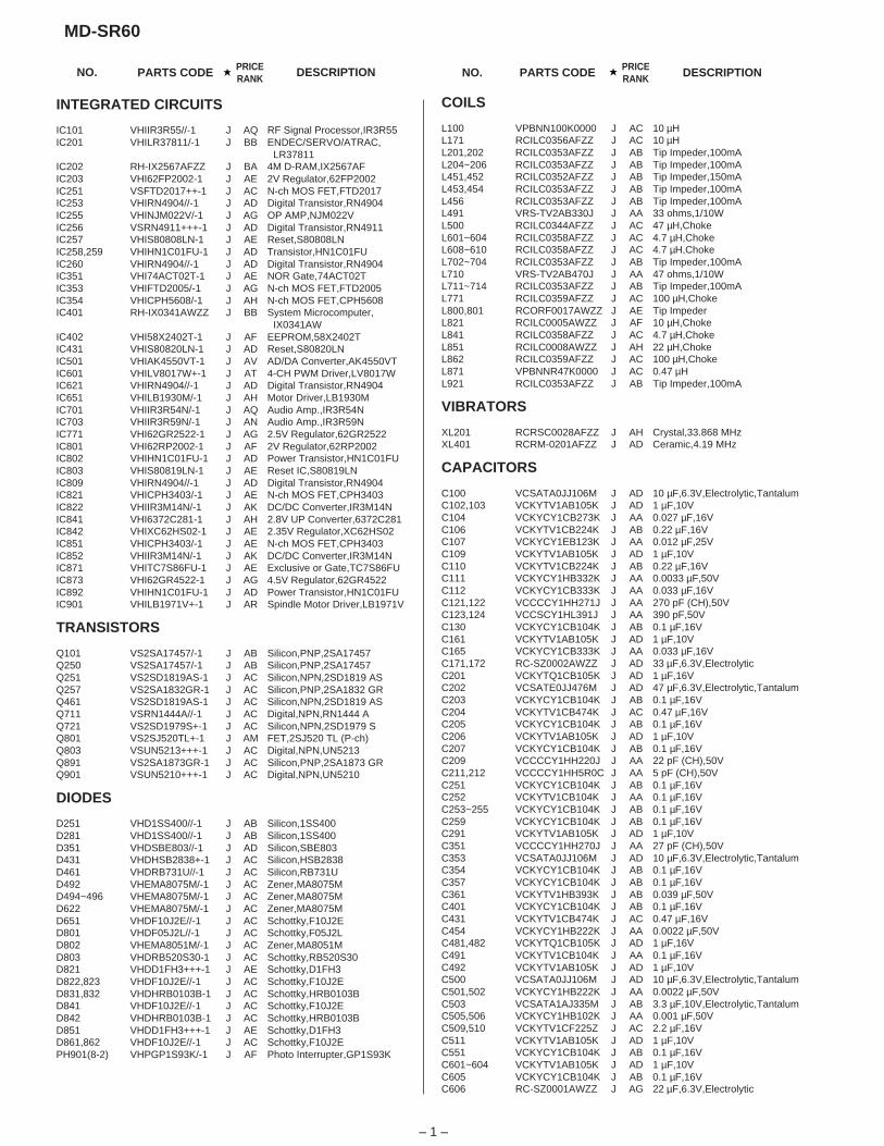
PRICERANK DESCRIPTIONNO. PARTS CODE NO. PARTS CODE PRICE
RANK DESCRIPTION
MD-SR60
– 1 –
INTEGRATED CIRCUITS
IC101 VHIIR3R55//-1 J AQ RF Signal Processor,IR3R55IC201 VHILR37811/-1 J BB ENDEC/SERVO/ATRAC,
LR37811IC202 RH-IX2567AFZZ J BA 4M D-RAM,IX2567AFIC203 VHI62FP2002-1 J AE 2V Regulator,62FP2002IC251 VSFTD2017++-1 J AC N-ch MOS FET,FTD2017IC253 VHIRN4904//-1 J AD Digital Transistor,RN4904IC255 VHINJM022V/-1 J AG OP AMP,NJM022VIC256 VSRN4911+++-1 J AD Digital Transistor,RN4911IC257 VHIS80808LN-1 J AE Reset,S80808LNIC258,259 VHIHN1C01FU-1 J AD Transistor,HN1C01FUIC260 VHIRN4904//-1 J AD Digital Transistor,RN4904IC351 VHI74ACT02T-1 J AE NOR Gate,74ACT02TIC353 VHIFTD2005/-1 J AG N-ch MOS FET,FTD2005IC354 VHICPH5608/-1 J AH N-ch MOS FET,CPH5608IC401 RH-IX0341AWZZ J BB System Microcomputer,
IX0341AWIC402 VHI58X2402T-1 J AF EEPROM,58X2402TIC431 VHIS80820LN-1 J AD Reset,S80820LNIC501 VHIAK4550VT-1 J AV AD/DA Converter,AK4550VTIC601 VHILV8017W+-1 J AT 4-CH PWM Driver,LV8017WIC621 VHIRN4904//-1 J AD Digital Transistor,RN4904IC651 VHILB1930M/-1 J AH Motor Driver,LB1930MIC701 VHIIR3R54N/-1 J AQ Audio Amp.,IR3R54NIC703 VHIIR3R59N/-1 J AN Audio Amp.,IR3R59NIC771 VHI62GR2522-1 J AG 2.5V Regulator,62GR2522IC801 VHI62RP2002-1 J AF 2V Regulator,62RP2002IC802 VHIHN1C01FU-1 J AD Power Transistor,HN1C01FUIC803 VHIS80819LN-1 J AE Reset IC,S80819LNIC809 VHIRN4904//-1 J AD Digital Transistor,RN4904IC821 VHICPH3403/-1 J AE N-ch MOS FET,CPH3403IC822 VHIIR3M14N/-1 J AK DC/DC Converter,IR3M14NIC841 VHI6372C281-1 J AH 2.8V UP Converter,6372C281IC842 VHIXC62HS02-1 J AE 2.35V Regulator,XC62HS02IC851 VHICPH3403/-1 J AE N-ch MOS FET,CPH3403IC852 VHIIR3M14N/-1 J AK DC/DC Converter,IR3M14NIC871 VHITC7S86FU-1 J AE Exclusive or Gate,TC7S86FUIC873 VHI62GR4522-1 J AG 4.5V Regulator,62GR4522IC892 VHIHN1C01FU-1 J AD Power Transistor,HN1C01FUIC901 VHILB1971V+-1 J AR Spindle Motor Driver,LB1971V
TRANSISTORS
Q101 VS2SA17457/-1 J AB Silicon,PNP,2SA17457Q250 VS2SA17457/-1 J AB Silicon,PNP,2SA17457Q251 VS2SD1819AS-1 J AC Silicon,NPN,2SD1819 ASQ257 VS2SA1832GR-1 J AC Silicon,PNP,2SA1832 GRQ461 VS2SD1819AS-1 J AC Silicon,NPN,2SD1819 ASQ711 VSRN1444A//-1 J AC Digital,NPN,RN1444 AQ721 VS2SD1979S+-1 J AC Silicon,NPN,2SD1979 SQ801 VS2SJ520TL+-1 J AM FET,2SJ520 TL (P-ch)Q803 VSUN5213+++-1 J AC Digital,NPN,UN5213Q891 VS2SA1873GR-1 J AC Silicon,PNP,2SA1873 GRQ901 VSUN5210+++-1 J AC Digital,NPN,UN5210
DIODES
D251 VHD1SS400//-1 J AB Silicon,1SS400D281 VHD1SS400//-1 J AB Silicon,1SS400D351 VHDSBE803//-1 J AD Silicon,SBE803D431 VHDHSB2838+-1 J AC Silicon,HSB2838D461 VHDRB731U//-1 J AC Silicon,RB731UD492 VHEMA8075M/-1 J AC Zener,MA8075MD494~496 VHEMA8075M/-1 J AC Zener,MA8075MD622 VHEMA8075M/-1 J AC Zener,MA8075MD651 VHDF10J2E//-1 J AC Schottky,F10J2ED801 VHDF05J2L//-1 J AC Schottky,F05J2LD802 VHEMA8051M/-1 J AC Zener,MA8051MD803 VHDRB520S30-1 J AC Schottky,RB520S30D821 VHDD1FH3+++-1 J AE Schottky,D1FH3D822,823 VHDF10J2E//-1 J AC Schottky,F10J2ED831,832 VHDHRB0103B-1 J AC Schottky,HRB0103BD841 VHDF10J2E//-1 J AC Schottky,F10J2ED842 VHDHRB0103B-1 J AC Schottky,HRB0103BD851 VHDD1FH3+++-1 J AE Schottky,D1FH3D861,862 VHDF10J2E//-1 J AC Schottky,F10J2EPH901(8-2) VHPGP1S93K/-1 J AF Photo Interrupter,GP1S93K
COILS
L100 VPBNN100K0000 J AC 10 µHL171 RCILC0356AFZZ J AC 10 µHL201,202 RCILC0353AFZZ J AB Tip Impeder,100mAL204~206 RCILC0353AFZZ J AB Tip Impeder,100mAL451,452 RCILC0352AFZZ J AB Tip Impeder,150mAL453,454 RCILC0353AFZZ J AB Tip Impeder,100mAL456 RCILC0353AFZZ J AB Tip Impeder,100mAL491 VRS-TV2AB330J J AA 33 ohms,1/10WL500 RCILC0344AFZZ J AC 47 µH,ChokeL601~604 RCILC0358AFZZ J AC 4.7 µH,ChokeL608~610 RCILC0358AFZZ J AC 4.7 µH,ChokeL702~704 RCILC0353AFZZ J AB Tip Impeder,100mAL710 VRS-TV2AB470J J AA 47 ohms,1/10WL711~714 RCILC0353AFZZ J AB Tip Impeder,100mAL771 RCILC0359AFZZ J AC 100 µH,ChokeL800,801 RCORF0017AWZZ J AE Tip ImpederL821 RCILC0005AWZZ J AF 10 µH,ChokeL841 RCILC0358AFZZ J AC 4.7 µH,ChokeL851 RCILC0008AWZZ J AH 22 µH,ChokeL862 RCILC0359AFZZ J AC 100 µH,ChokeL871 VPBNNR47K0000 J AC 0.47 µHL921 RCILC0353AFZZ J AB Tip Impeder,100mA
VIBRATORS
XL201 RCRSC0028AFZZ J AH Crystal,33.868 MHzXL401 RCRM-0201AFZZ J AD Ceramic,4.19 MHz
CAPACITORS
C100 VCSATA0JJ106M J AD 10 µF,6.3V,Electrolytic,TantalumC102,103 VCKYTV1AB105K J AD 1 µF,10VC104 VCKYCY1CB273K J AA 0.027 µF,16VC106 VCKYTV1CB224K J AB 0.22 µF,16VC107 VCKYCY1EB123K J AA 0.012 µF,25VC109 VCKYTV1AB105K J AD 1 µF,10VC110 VCKYTV1CB224K J AB 0.22 µF,16VC111 VCKYCY1HB332K J AA 0.0033 µF,50VC112 VCKYCY1CB333K J AA 0.033 µF,16VC121,122 VCCCCY1HH271J J AA 270 pF (CH),50VC123,124 VCCSCY1HL391J J AA 390 pF,50VC130 VCKYCY1CB104K J AB 0.1 µF,16VC161 VCKYTV1AB105K J AD 1 µF,10VC165 VCKYCY1CB333K J AA 0.033 µF,16VC171,172 RC-SZ0002AWZZ J AD 33 µF,6.3V,ElectrolyticC201 VCKYTQ1CB105K J AD 1 µF,16VC202 VCSATE0JJ476M J AD 47 µF,6.3V,Electrolytic,TantalumC203 VCKYCY1CB104K J AB 0.1 µF,16VC204 VCKYTV1CB474K J AC 0.47 µF,16VC205 VCKYCY1CB104K J AB 0.1 µF,16VC206 VCKYTV1AB105K J AD 1 µF,10VC207 VCKYCY1CB104K J AB 0.1 µF,16VC209 VCCCCY1HH220J J AA 22 pF (CH),50VC211,212 VCCCCY1HH5R0C J AA 5 pF (CH),50VC251 VCKYCY1CB104K J AB 0.1 µF,16VC252 VCKYTV1CB104K J AA 0.1 µF,16VC253~255 VCKYCY1CB104K J AB 0.1 µF,16VC259 VCKYCY1CB104K J AB 0.1 µF,16VC291 VCKYTV1AB105K J AD 1 µF,10VC351 VCCCCY1HH270J J AA 27 pF (CH),50VC353 VCSATA0JJ106M J AD 10 µF,6.3V,Electrolytic,TantalumC354 VCKYCY1CB104K J AB 0.1 µF,16VC357 VCKYCY1CB104K J AB 0.1 µF,16VC361 VCKYTV1HB393K J AB 0.039 µF,50VC401 VCKYCY1CB104K J AB 0.1 µF,16VC431 VCKYTV1CB474K J AC 0.47 µF,16VC454 VCKYCY1HB222K J AA 0.0022 µF,50VC481,482 VCKYTQ1CB105K J AD 1 µF,16VC491 VCKYTV1CB104K J AA 0.1 µF,16VC492 VCKYTV1AB105K J AD 1 µF,10VC500 VCSATA0JJ106M J AD 10 µF,6.3V,Electrolytic,TantalumC501,502 VCKYCY1HB222K J AA 0.0022 µF,50VC503 VCSATA1AJ335M J AB 3.3 µF,10V,Electrolytic,TantalumC505,506 VCKYCY1HB102K J AA 0.001 µF,50VC509,510 VCKYTV1CF225Z J AC 2.2 µF,16VC511 VCKYTV1AB105K J AD 1 µF,10VC551 VCKYCY1CB104K J AB 0.1 µF,16VC601~604 VCKYTV1AB105K J AD 1 µF,10VC605 VCKYCY1CB104K J AB 0.1 µF,16VC606 RC-SZ0001AWZZ J AG 22 µF,6.3V,Electrolytic
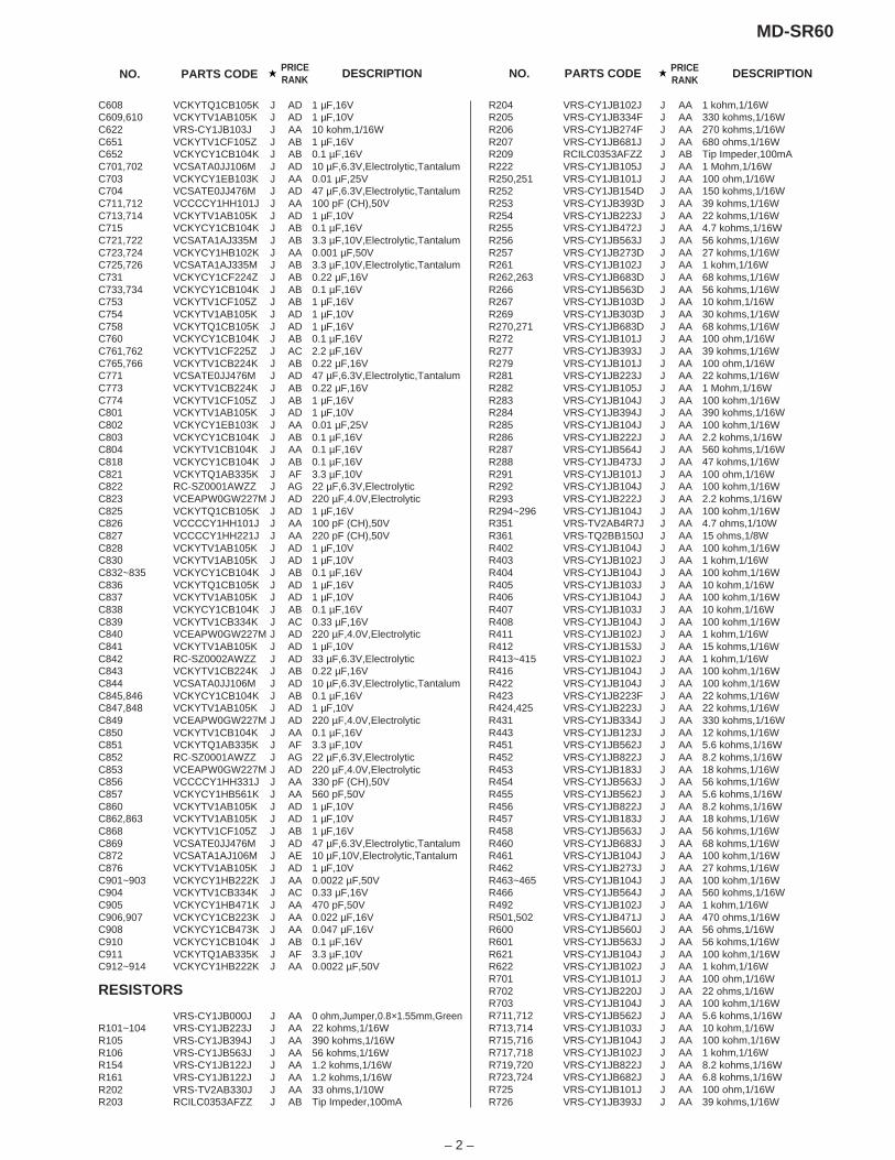
NO. PRICERANK DESCRIPTIONPARTS CODENO. PARTS CODE
PRICERANK DESCRIPTION
MD-SR60
C608 VCKYTQ1CB105K J AD 1 µF,16VC609,610 VCKYTV1AB105K J AD 1 µF,10VC622 VRS-CY1JB103J J AA 10 kohm,1/16WC651 VCKYTV1CF105Z J AB 1 µF,16VC652 VCKYCY1CB104K J AB 0.1 µF,16VC701,702 VCSATA0JJ106M J AD 10 µF,6.3V,Electrolytic,TantalumC703 VCKYCY1EB103K J AA 0.01 µF,25VC704 VCSATE0JJ476M J AD 47 µF,6.3V,Electrolytic,TantalumC711,712 VCCCCY1HH101J J AA 100 pF (CH),50VC713,714 VCKYTV1AB105K J AD 1 µF,10VC715 VCKYCY1CB104K J AB 0.1 µF,16VC721,722 VCSATA1AJ335M J AB 3.3 µF,10V,Electrolytic,TantalumC723,724 VCKYCY1HB102K J AA 0.001 µF,50VC725,726 VCSATA1AJ335M J AB 3.3 µF,10V,Electrolytic,TantalumC731 VCKYCY1CF224Z J AB 0.22 µF,16VC733,734 VCKYCY1CB104K J AB 0.1 µF,16VC753 VCKYTV1CF105Z J AB 1 µF,16VC754 VCKYTV1AB105K J AD 1 µF,10VC758 VCKYTQ1CB105K J AD 1 µF,16VC760 VCKYCY1CB104K J AB 0.1 µF,16VC761,762 VCKYTV1CF225Z J AC 2.2 µF,16VC765,766 VCKYTV1CB224K J AB 0.22 µF,16VC771 VCSATE0JJ476M J AD 47 µF,6.3V,Electrolytic,TantalumC773 VCKYTV1CB224K J AB 0.22 µF,16VC774 VCKYTV1CF105Z J AB 1 µF,16VC801 VCKYTV1AB105K J AD 1 µF,10VC802 VCKYCY1EB103K J AA 0.01 µF,25VC803 VCKYCY1CB104K J AB 0.1 µF,16VC804 VCKYTV1CB104K J AA 0.1 µF,16VC818 VCKYCY1CB104K J AB 0.1 µF,16VC821 VCKYTQ1AB335K J AF 3.3 µF,10VC822 RC-SZ0001AWZZ J AG 22 µF,6.3V,ElectrolyticC823 VCEAPW0GW227M J AD 220 µF,4.0V,ElectrolyticC825 VCKYTQ1CB105K J AD 1 µF,16VC826 VCCCCY1HH101J J AA 100 pF (CH),50VC827 VCCCCY1HH221J J AA 220 pF (CH),50VC828 VCKYTV1AB105K J AD 1 µF,10VC830 VCKYTV1AB105K J AD 1 µF,10VC832~835 VCKYCY1CB104K J AB 0.1 µF,16VC836 VCKYTQ1CB105K J AD 1 µF,16VC837 VCKYTV1AB105K J AD 1 µF,10VC838 VCKYCY1CB104K J AB 0.1 µF,16VC839 VCKYTV1CB334K J AC 0.33 µF,16VC840 VCEAPW0GW227M J AD 220 µF,4.0V,ElectrolyticC841 VCKYTV1AB105K J AD 1 µF,10VC842 RC-SZ0002AWZZ J AD 33 µF,6.3V,ElectrolyticC843 VCKYTV1CB224K J AB 0.22 µF,16VC844 VCSATA0JJ106M J AD 10 µF,6.3V,Electrolytic,TantalumC845,846 VCKYCY1CB104K J AB 0.1 µF,16VC847,848 VCKYTV1AB105K J AD 1 µF,10VC849 VCEAPW0GW227M J AD 220 µF,4.0V,ElectrolyticC850 VCKYTV1CB104K J AA 0.1 µF,16VC851 VCKYTQ1AB335K J AF 3.3 µF,10VC852 RC-SZ0001AWZZ J AG 22 µF,6.3V,ElectrolyticC853 VCEAPW0GW227M J AD 220 µF,4.0V,ElectrolyticC856 VCCCCY1HH331J J AA 330 pF (CH),50VC857 VCKYCY1HB561K J AA 560 pF,50VC860 VCKYTV1AB105K J AD 1 µF,10VC862,863 VCKYTV1AB105K J AD 1 µF,10VC868 VCKYTV1CF105Z J AB 1 µF,16VC869 VCSATE0JJ476M J AD 47 µF,6.3V,Electrolytic,TantalumC872 VCSATA1AJ106M J AE 10 µF,10V,Electrolytic,TantalumC876 VCKYTV1AB105K J AD 1 µF,10VC901~903 VCKYCY1HB222K J AA 0.0022 µF,50VC904 VCKYTV1CB334K J AC 0.33 µF,16VC905 VCKYCY1HB471K J AA 470 pF,50VC906,907 VCKYCY1CB223K J AA 0.022 µF,16VC908 VCKYCY1CB473K J AA 0.047 µF,16VC910 VCKYCY1CB104K J AB 0.1 µF,16VC911 VCKYTQ1AB335K J AF 3.3 µF,10VC912~914 VCKYCY1HB222K J AA 0.0022 µF,50V
RESISTORS
VRS-CY1JB000J J AA 0 ohm,Jumper,0.8×1.55mm,GreenR101~104 VRS-CY1JB223J J AA 22 kohms,1/16WR105 VRS-CY1JB394J J AA 390 kohms,1/16WR106 VRS-CY1JB563J J AA 56 kohms,1/16WR154 VRS-CY1JB122J J AA 1.2 kohms,1/16WR161 VRS-CY1JB122J J AA 1.2 kohms,1/16WR202 VRS-TV2AB330J J AA 33 ohms,1/10WR203 RCILC0353AFZZ J AB Tip Impeder,100mA
R204 VRS-CY1JB102J J AA 1 kohm,1/16WR205 VRS-CY1JB334F J AA 330 kohms,1/16WR206 VRS-CY1JB274F J AA 270 kohms,1/16WR207 VRS-CY1JB681J J AA 680 ohms,1/16WR209 RCILC0353AFZZ J AB Tip Impeder,100mAR222 VRS-CY1JB105J J AA 1 Mohm,1/16WR250,251 VRS-CY1JB101J J AA 100 ohm,1/16WR252 VRS-CY1JB154D J AA 150 kohms,1/16WR253 VRS-CY1JB393D J AA 39 kohms,1/16WR254 VRS-CY1JB223J J AA 22 kohms,1/16WR255 VRS-CY1JB472J J AA 4.7 kohms,1/16WR256 VRS-CY1JB563J J AA 56 kohms,1/16WR257 VRS-CY1JB273D J AA 27 kohms,1/16WR261 VRS-CY1JB102J J AA 1 kohm,1/16WR262,263 VRS-CY1JB683D J AA 68 kohms,1/16WR266 VRS-CY1JB563D J AA 56 kohms,1/16WR267 VRS-CY1JB103D J AA 10 kohm,1/16WR269 VRS-CY1JB303D J AA 30 kohms,1/16WR270,271 VRS-CY1JB683D J AA 68 kohms,1/16WR272 VRS-CY1JB101J J AA 100 ohm,1/16WR277 VRS-CY1JB393J J AA 39 kohms,1/16WR279 VRS-CY1JB101J J AA 100 ohm,1/16WR281 VRS-CY1JB223J J AA 22 kohms,1/16WR282 VRS-CY1JB105J J AA 1 Mohm,1/16WR283 VRS-CY1JB104J J AA 100 kohm,1/16WR284 VRS-CY1JB394J J AA 390 kohms,1/16WR285 VRS-CY1JB104J J AA 100 kohm,1/16WR286 VRS-CY1JB222J J AA 2.2 kohms,1/16WR287 VRS-CY1JB564J J AA 560 kohms,1/16WR288 VRS-CY1JB473J J AA 47 kohms,1/16WR291 VRS-CY1JB101J J AA 100 ohm,1/16WR292 VRS-CY1JB104J J AA 100 kohm,1/16WR293 VRS-CY1JB222J J AA 2.2 kohms,1/16WR294~296 VRS-CY1JB104J J AA 100 kohm,1/16WR351 VRS-TV2AB4R7J J AA 4.7 ohms,1/10WR361 VRS-TQ2BB150J J AA 15 ohms,1/8WR402 VRS-CY1JB104J J AA 100 kohm,1/16WR403 VRS-CY1JB102J J AA 1 kohm,1/16WR404 VRS-CY1JB104J J AA 100 kohm,1/16WR405 VRS-CY1JB103J J AA 10 kohm,1/16WR406 VRS-CY1JB104J J AA 100 kohm,1/16WR407 VRS-CY1JB103J J AA 10 kohm,1/16WR408 VRS-CY1JB104J J AA 100 kohm,1/16WR411 VRS-CY1JB102J J AA 1 kohm,1/16WR412 VRS-CY1JB153J J AA 15 kohms,1/16WR413~415 VRS-CY1JB102J J AA 1 kohm,1/16WR416 VRS-CY1JB104J J AA 100 kohm,1/16WR422 VRS-CY1JB104J J AA 100 kohm,1/16WR423 VRS-CY1JB223F J AA 22 kohms,1/16WR424,425 VRS-CY1JB223J J AA 22 kohms,1/16WR431 VRS-CY1JB334J J AA 330 kohms,1/16WR443 VRS-CY1JB123J J AA 12 kohms,1/16WR451 VRS-CY1JB562J J AA 5.6 kohms,1/16WR452 VRS-CY1JB822J J AA 8.2 kohms,1/16WR453 VRS-CY1JB183J J AA 18 kohms,1/16WR454 VRS-CY1JB563J J AA 56 kohms,1/16WR455 VRS-CY1JB562J J AA 5.6 kohms,1/16WR456 VRS-CY1JB822J J AA 8.2 kohms,1/16WR457 VRS-CY1JB183J J AA 18 kohms,1/16WR458 VRS-CY1JB563J J AA 56 kohms,1/16WR460 VRS-CY1JB683J J AA 68 kohms,1/16WR461 VRS-CY1JB104J J AA 100 kohm,1/16WR462 VRS-CY1JB273J J AA 27 kohms,1/16WR463~465 VRS-CY1JB104J J AA 100 kohm,1/16WR466 VRS-CY1JB564J J AA 560 kohms,1/16WR492 VRS-CY1JB102J J AA 1 kohm,1/16WR501,502 VRS-CY1JB471J J AA 470 ohms,1/16WR600 VRS-CY1JB560J J AA 56 ohms,1/16WR601 VRS-CY1JB563J J AA 56 kohms,1/16WR621 VRS-CY1JB104J J AA 100 kohm,1/16WR622 VRS-CY1JB102J J AA 1 kohm,1/16WR701 VRS-CY1JB101J J AA 100 ohm,1/16WR702 VRS-CY1JB220J J AA 22 ohms,1/16WR703 VRS-CY1JB104J J AA 100 kohm,1/16WR711,712 VRS-CY1JB562J J AA 5.6 kohms,1/16WR713,714 VRS-CY1JB103J J AA 10 kohm,1/16WR715,716 VRS-CY1JB104J J AA 100 kohm,1/16WR717,718 VRS-CY1JB102J J AA 1 kohm,1/16WR719,720 VRS-CY1JB822J J AA 8.2 kohms,1/16WR723,724 VRS-CY1JB682J J AA 6.8 kohms,1/16WR725 VRS-CY1JB101J J AA 100 ohm,1/16WR726 VRS-CY1JB393J J AA 39 kohms,1/16W
– 2 –
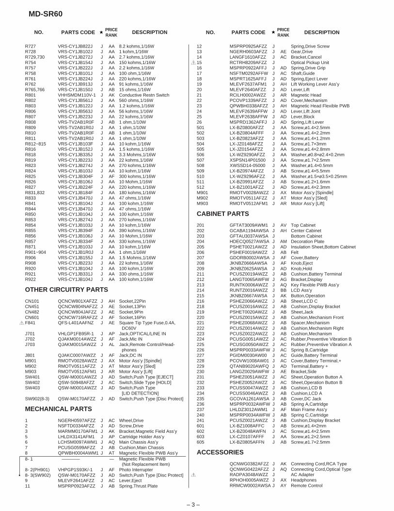
PRICERANK DESCRIPTIONNO. PARTS CODE NO. PARTS CODE PRICE
RANK DESCRIPTION
MD-SR60
R727 VRS-CY1JB822J J AA 8.2 kohms,1/16WR728 VRS-CY1JB102J J AA 1 kohm,1/16WR729,730 VRS-CY1JB272J J AA 2.7 kohms,1/16WR754 VRS-CY1JB154J J AA 150 kohms,1/16WR757 VRS-CY1JB222J J AA 2.2 kohms,1/16WR758 VRS-CY1JB101J J AA 100 ohm,1/16WR761 VRS-CY1JB224J J AA 220 kohms,1/16WR762 VRS-CY1JB913J J AA 91 kohms,1/16WR765,766 VRS-CY1JB150J J AB 15 ohms,1/16WR801 VHHSMDM110V-1 J AK Conductive Restn SwitchR802 VRS-CY1JB561J J AA 560 ohms,1/16WR803 VRS-CY1JB122J J AA 1.2 kohms,1/16WR806 VRS-CY1JB563J J AA 56 kohms,1/16WR807 VRS-CY1JB223J J AA 22 kohms,1/16WR808 VRS-TV2AB1R0F J AB 1 ohm,1/10WR809 VRS-TV2AB1R0J J AA 1 ohm,1/10WR810 VRS-TV2AB1R0F J AB 1 ohm,1/10WR811 VRS-TV2AB1R0J J AA 1 ohm,1/10WR812~815 VRS-CY1JB103F J AA 10 kohm,1/16WR816 VRS-CY1JB152J J AA 1.5 kohms,1/16WR818 VRS-CY1JB335J J AA 3.3 Mohms,1/16WR819 VRS-CY1JB223J J AA 22 kohms,1/16WR823 VRS-CY1JB274J J AA 270 kohms,1/16WR824 VRS-CY1JB103J J AA 10 kohm,1/16WR825 VRS-CY1JB304F J AF 300 kohms,1/16WR826 VRS-CY1JB106J J AA 10 Mohm,1/16WR827 VRS-CY1JB224F J AA 220 kohms,1/16WR831,832 VRS-CY1JB184F J AA 180 kohms,1/16WR833 VRS-CY1JB470J J AA 47 ohms,1/16WR841 VRS-CY1JB104J J AA 100 kohm,1/16WR844 VRS-CY1JB470J J AA 47 ohms,1/16WR850 VRS-CY1JB104J J AA 100 kohm,1/16WR853 VRS-CY1JB274J J AA 270 kohms,1/16WR854 VRS-CY1JB103J J AA 10 kohm,1/16WR855 VRS-CY1JB394F J AA 390 kohms,1/16WR856 VRS-CY1JB106J J AA 10 Mohm,1/16WR857 VRS-CY1JB334F J AA 330 kohms,1/16WR871 VRS-CY1JB103J J AA 10 kohm,1/16WR901~904 VRS-CY1JB1R0J J AA 1 ohm,1/16WR906 VRS-CY1JB155J J AA 1.5 Mohms,1/16WR908 VRS-CY1JB223J J AA 22 kohms,1/16WR920 VRS-CY1JB104J J AA 100 kohm,1/16WR921 VRS-CY1JB331J J AA 330 ohms,1/16WR922 VRS-CY1JB104J J AA 100 kohm,1/16W
OTHER CIRCUITRY PARTS
CN101 QCNCW801XAFZZ J AH Socket,22PinCN451 QCNCW804NAFZZ J AE Socket,13PinCN482 QCNCW804JAFZZ J AE Socket,9PinCN601 QCNCW716RAFZZ J AF Socket,16Pin
! F841 QFS-L401AAFNZ J AE Square Tip Type Fuse,0.4A,DC60V
J701 VHLGP1FB95R-1 J AP Jack,OPTICAL/LINE INJ702 QJAKM0014AWZZ J AF Jack,Mic INJ703 QJAKM0015AWZZ J AL Jack,Remote Control/Head-
phonesJ801 QJAKC0007AWZZ J AF Jack,DC INM901 RMOTV0028AWZZ J AX Motor Ass’y [Spindle]M902 RMOTV0511AFZZ J AT Motor Ass’y [Sled]M903 RMOTV0512AFM1 J AR Motor Ass’y [Lift]SW401 QSW-M0001AWZZ J AD Switch,Push Type [EJECT]SW402 QSW-S0948AFZZ J AC Switch,Slide Type [HOLD]SW403 QSW-M0001AWZZ J AD Switch,Push Type
[LID DETECTION]SW902(8-3) QSW-M0170AFZZ J AD Switch,Push Type [Disc Protect]
MECHANICAL PARTS
1 NGERH0597AFZZ J AC Wheel,Drive2 NSFTD0334AFZZ J AD Screw,Drive3 MARMM0170AFM1 J AK Bracket,Magnetic Field Ass’y5 LHLDX3141AFM1 J AP Cartridge Holder Ass’y6 LCHSM0097AWM1 J AQ Main Chassis Ass’y7 PCUSG0599AFZZ J AB Cushion,Main Chassis8 QPWBH0004AWM1 J AT Magnetic Flexible PWB Ass’y8- 1 ———— — Magnetic Flexible PWB
(Not Replacement Item)8- 2(PH901) VHPGP1S93K/-1 J AF Photo Interrupter8- 3(SW902) QSW-M0170AFZZ J AD Switch,Push Type [Disc Protect]9 MLEVF2641AFZZ J AC Lever,Eject11 MSPRP0923AFZZ J AB Spring,Thrust Plate
12 MSPRP0925AFZZ J Spring,Drive Screw13 NGERH0603AFZZ J AE Gear,Drive14 LANGF1610AFZZ J AC Bracket,Cancel
! 15 RCTRH8209AFZZ J Optical Pickup Unit16 MSPRP0922AFFJ J AD Spring,Drive Grip17 NSFTM0292AFFW J AC Shaft,Guide18 MSPRT1625AFFJ J AD Spring,Eject Lever19 MLEVF2637AFM1 J AH Lift Working Lever Ass’y20 MLEVF2640AFZZ J AD Lever,Lift21 RCILH0002AWZZ J AR Magnetic Head22 PCOVP1339AFZZ J AD Cover,Mechanism23 QPWBH0338AFZZ J AH Magnetic Head Flexible PWB24 MLEVF2639AFFW J AD Lever,Lift Joint25 MLEVF2638AFFW J AD Lever,Block26 MSPRD1362AFFJ J AD Spring,Lift Lever501 LX-BZ0800AFZZ J AA Screw,ø1.4×2.5mm502 LX-BZ0804AFFF J AA Screw,ø1.4×2.2mm503 LX-BZ0823AFZZ J AA Screw,ø1.4×1.2mm504 LX-JZ0148AFZZ J AA Screw,ø1.7×3mm505 LX-JZ0154AFZZ J AA Screw,ø1.4×2.8mm506 LX-WZ9290AFZZ J AA Washer,ø0.8×ø2.4×0.2mm507 XSPSN14P01500 J AA Screw,ø1.7×2.5mm508 XWSSD14-05000 J AA Washer,ø1.4×0.5mm509 LX-BZ0974AFZZ J AB Screw,ø1.4×5.5mm510 LX-WZ9296AFZZ J AA Washer,ø1.5×ø3.5×0.25mm511 LX-BZ0991AFZZ J AB Screw,ø1.2×1.6mm512 LX-BZ1001AFZZ J AD Screw,ø1.4×2.3mmM901 RMOTV0028AWZZ J AX Motor Ass’y [Spindle]M902 RMOTV0511AFZZ J AT Motor Ass’y [Sled]M903 RMOTV0512AFM1 J AR Motor Ass’y [Lift]
CABINET PARTS
201 GFTAT3009AWM1 J AV Top Cabinet202 GCABA1194AWSA J AH Center Cabinet203 GFTAU3037AWSA J Bottom Cabinet204 HDECQ0527AWSA J AM Decoration Plate205 PSHET0021AWZZ J AD Insulation Sheet,Bottom Cabinet206 PSHEF0019AWZZ J AB Felt207 GDORB0002AWSA J AF Cover,Battery208 JKNBZ0666AWSA J AF Knob,Eject209 JKNBZ0625AWSA J AD Knob,Hold211 PCUSZ0019AWZZ J AB Cushion,Battery Terminal212 LANGT0065AWFW J AG Bracket,Display213 RUNTK0006AWZZ J AQ Key Flexible PWB Ass’y214 RUNTZ0016AWZZ J BB LCD Ass’y215 JKNBZ0667AWSA J AK Button,Operation216 PSHEZ0066AWZZ J AB Sheet,LCD C218 PCUSZ0016AWZZ J AB Cushion,Display Bracket219 PSHET0020AWZZ J AB Sheet,Jack220 PCUSZ0015AWZZ J AB Cushion,Mechanism Front221 PSHEZ0068AWZZ J AB Spacer,Mechanism222 PCUSZ0014AWZZ J AB Cushion,Mechanism Right223 PCUSZ0022AWZZ J AB Cushion,Mechanism224 PCUSG0051AWZZ J AC Rubber,Preventive Vibration B225 PCUSG0050AWZZ J AC Rubber,Preventive Vibration A226 MSPRP0033AWFW J AC Spring B,Cartridge227 PGIDM0030AW00 J AC Guide,Battery Terminal228 PCOVW1008AW01 J AC Cover,Battery Terminal,+229 QTANB9020AWFQ J AD Terminal,Battery +230 LANGZ0029AWFW J AE Bracket,Side231 PSHEZ0051AWZZ J AC Sheet,Operation Button A232 PSHEZ0052AWZZ J AC Sheet,Operation Button B233 PCUSS0047AWZZ J AB Cushion,LCD B234 PCUSS0046AWZZ J AB Cushion,LCD A235 GCOVA1261AWSA J AB Cover,DC Jack236 MSPRP0032AWFW J AB Spring A,Cartridge237 LHLDZ3012AWM1 J AF Main Frame Ass’y240 MSPRP0034AWFW J AB Spring C,Cartridge241 PCUSZ0021AWZZ J AB Cushion,Display Bracket601 LX-BZ1008AFFC J AB Screw,ø1.4×2mm602 LX-BZ0048AWFN J AC Screw,ø1.4×2.5mm603 LX-CZ0107AFFF J AA Screw,ø1.2×2.5mm605 LX-BZ0805AFFN J AB Screw,ø1.7×2.5mm
ACCESSORIES
QCNWG0382AFZZ J AK Connecting Cord,RCA TypeQCNWG0422AFZZ J AQ Connecting Cord,Optical Type
! RADPA3048AWZZ J AC AdapterRPHOH0005AWZZ J AX HeadphonesRRMCW0002AWSA J AY Remote Control
– 3 –
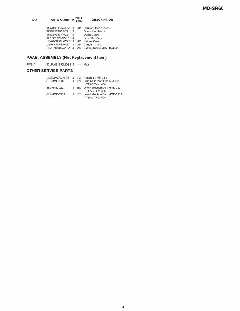
NO. PARTS CODEPRICERANK DESCRIPTION
MD-SR60
TCAUH0050AWZZ J AB Caution,HeadphonesTINSE0320AWZZ J Operation ManualTINSZ0586AWZZ J Quick GuideTLABR1127AWZZ J Label,Bar CodeUBAGC0003AWZZ J AD Battery CaseUBAGC0006AWSA J AH Carrying CaseUBATM0003AWSA J AR Battery,Nickel-Metal Hydride
P.W.B. ASSEMBLY (Not Replacement Item)
PWB-A 92LPWB3355MDSS J — Main
OTHER SERVICE PARTS
UDSKM0001AFZZ J AZ Recording Minidisc88GMMD-110 J BV High Reflection Disc MMD-110
(TEAC Test MD)88GMMD-212 J BU Low Reflection Disc MMD-212
(TEAC Test MD)88GMMD-213A J BT Low Reflection Disc MMD-213A
(TEAC Test MD)
– 4 –
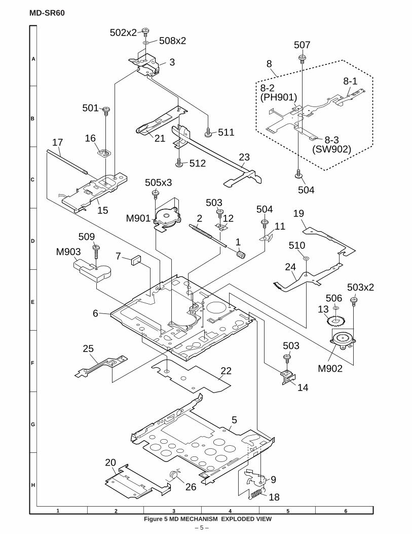
MD-SR60
A
B
C
D
E
F
G
H
1 2 3 4 5 6
Figure 5 MD MECHANISM EXPLODED VIEW– 5 –
M903
M902
M901
503x2
505x3
508x2502x2
3
501
21
23
5118-3
(SW902)
8-1
8
8-2(PH901)
504503
50412 19
11
1
2
1617
15
509510
24
50613
503
14
5
22
269
18
20
25
6
7
512
507
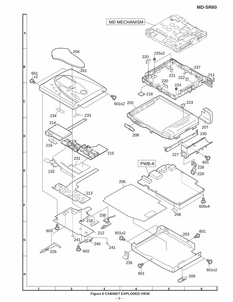
MD-SR60
A
B
C
D
E
F
G
H
1 2 3 4 5 6
Figure 6 CABINET EXPLODED VIEW– 6 –
204
MD MECHANISM
205
203
214
234 233
213
215
202
237
601x2
601x2
216
603
602
212
218236
601x2
601
601
601x2
209
PWB-A
208
220
220
221
219
229
223
222
207
224
225x2
240
226
201
241
241
235
605x4
228
227231
232
206
230
601
211
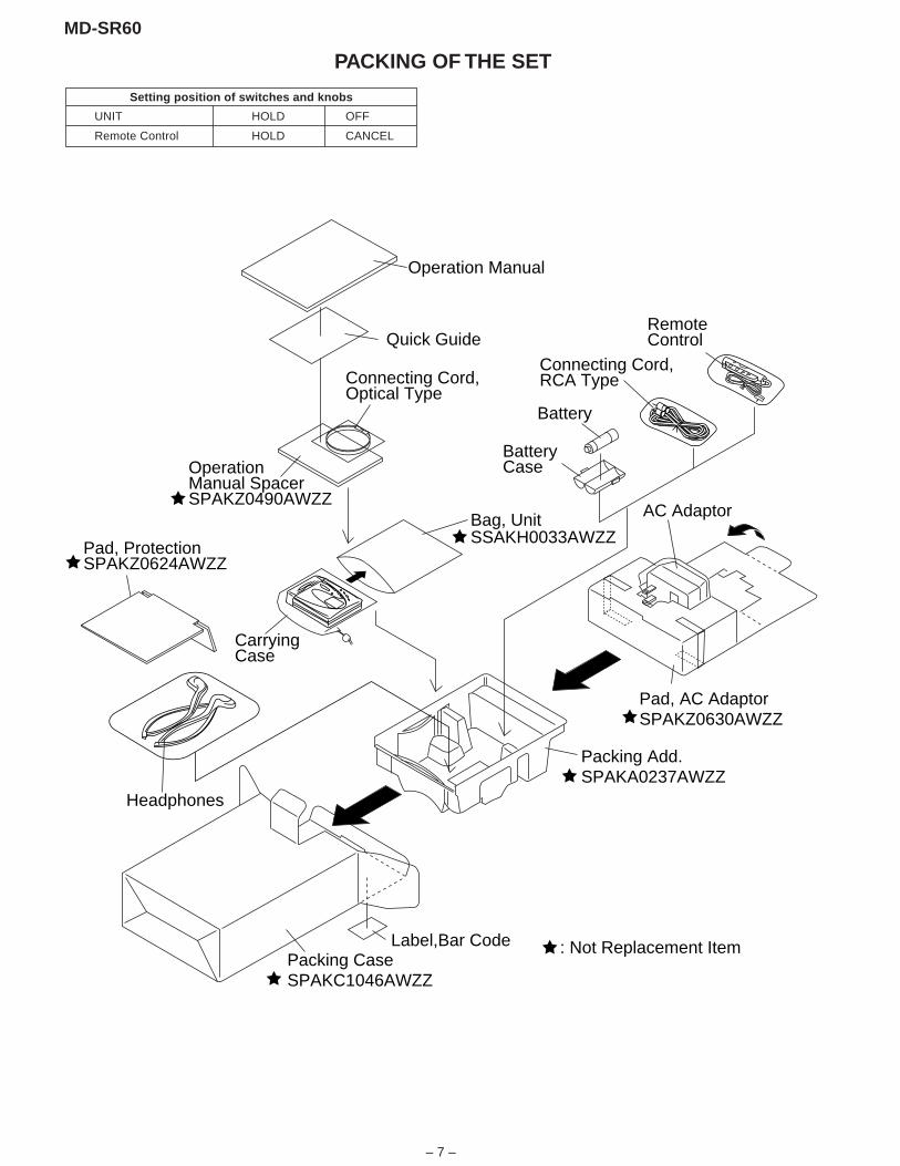
MD-SR60
PACKING OF THE SET
Setting position of switches and knobs
UNIT HOLD OFF
Remote Control HOLD CANCEL
– 7 –
Operation Manual SpacerSPAKZ0490AWZZ
Bag, UnitSSAKH0033AWZZ
Battery
Connecting Cord,RCA Type
AC Adaptor
Headphones
Remote Control
Packing Add.SPAKA0237AWZZ
Packing CaseSPAKC1046AWZZ
Pad, AC AdaptorSPAKZ0630AWZZ
Connecting Cord, Optical Type
Quick Guide
: Not Replacement Item
Carrying Case
Battery Case
Pad, ProtectionSPAKZ0624AWZZ
Operation Manual
Label,Bar Code

MD-SR60
— M E M O —
– 8 –

MD-SR60
COPYRIGHT 2000 BY SHARP CORPORATION
ALL RIGHTS RESERVED.
No part of this publication may be reproduced,stored in a retrieval system, or transmitted inany from or by any means, electronic, mechanical,photocopying, recording, or otherwise, withoutprior written permission of the publisher.
A0007-1766DS•HA•M
SC
SHARP CORPORATIONCommunication Systems GroupQuality & Reliability Control CenterHigashihiroshima, Hiroshima 739-0192, Japan
Printed in Japan
©