MB90437L (S) /438L (S) /F438L (S) MB90439 (S) /F439 (S) … · 2009-03-19 · MB90435 Series...
60
FUJITSU MICROELECTRONICS DATA SHEET Copyright©2002-2008 FUJITSU MICROELECTRONICS LIMITED All rights reserved 2008.8 The information for microcontroller supports is shown in the following homepage. Be sure to refer to the "Check Sheet" for the latest cautions on development. "Check Sheet" is seen at the following support page "Check Sheet" lists the minimal requirement items to be checked to prevent problems beforehand in system development. http://edevice.fujitsu.com/micom/en-support/ 16-bit Proprietary Microcontroller CMOS F 2 MC-16LX MB90435 Series MB90437L (S) /438L (S) /F438L (S) MB90439 (S) /F439 (S) /V540G ■ DESCRIPTION The MB90435 series with FLASH ROM is specially designed for industrial applications. The instruction set by F 2 MC-16LX CPU core inherits an AT architecture of the F 2 MC* family with additional instruction sets for high-level languages, extended addressing mode, enhanced multiplication/division instruc- tions, and enhanced bit manipulation instructions.The micro controller has a 32-bit accumulator for processing long word data. The MB90435 series has peripheral resources of 8/10-bit A/D converters, UART (SCI) , extended I/O serial interfaces, 8/16-bit timer, I/O timer (input capture (ICU) , output compare (OCU) ) . * : F 2 MC is the abbreviation of FUJITSU Flexible Microcontroller. ■ FEATURES • Clock Embedded PLL clock multiplication circuit Operating clock (PLL clock) can be selected from : divided-by-2 of oscillation or one to four times the oscillation Minimum instruction execution time : 62.5 ns (operation at oscillation of 4 MHz, four times the oscillation clock, VCC of 5.0 V) Subsystem Clock : 32 kHz (Continued) DS07-13727-2E
Transcript of MB90437L (S) /438L (S) /F438L (S) MB90439 (S) /F439 (S) … · 2009-03-19 · MB90435 Series...
FUJITSU MICROELECTRONICSDATA SHEET DS07-13727-2E
16-bit Proprietary MicrocontrollerCMOS
F2MC-16LX MB90435 SeriesMB90437L (S) /438L (S) /F438L (S) MB90439 (S) /F439 (S) /V540G DESCRIPTION
The MB90435 series with FLASH ROM is specially designed for industrial applications.
The instruction set by F2MC-16LX CPU core inherits an AT architecture of the F2MC* family with additionalinstruction sets for high-level languages, extended addressing mode, enhanced multiplication/division instruc-tions, and enhanced bit manipulation instructions.The micro controller has a 32-bit accumulator for processinglong word data. The MB90435 series has peripheral resources of 8/10-bit A/D converters, UART (SCI) , extended I/O serialinterfaces, 8/16-bit timer, I/O timer (input capture (ICU) , output compare (OCU) ) .
* : F2MC is the abbreviation of FUJITSU Flexible Microcontroller.
FEATURES• Clock
Embedded PLL clock multiplication circuitOperating clock (PLL clock) can be selected from : divided-by-2 of oscillation or one to four times the oscillationMinimum instruction execution time : 62.5 ns (operation at oscillation of 4 MHz, four times the oscillation clock,
VCC of 5.0 V) Subsystem Clock : 32 kHz
(Continued)
Copyright©2002-2008 FUJITSU MICROELECTRONICS LIMITED All rights reserved2008.8
The information for microcontroller supports is shown in the following homepage.Be sure to refer to the "Check Sheet" for the latest cautions on development.
"Check Sheet" is seen at the following support page"Check Sheet" lists the minimal requirement items to be checked to prevent problems beforehand in system development.
http://edevice.fujitsu.com/micom/en-support/
MB90435 Series
• Instruction set to optimize controller applicationsRich data types (bit, byte, word, long word) Rich addressing mode (23 types) Enhanced signed multiplication/division instruction and RETI instruction functionsEnhanced precision calculation realized by the 32-bit accumulator
• Instruction set designed for high level language (C language) and multi-task operationsAdoption of system stack pointer Enhanced pointer indirect instructionsBarrel shift instructions
• Program patch function (for two address pointers) • Enhanced execution speed : 4-byte Instruction queue• Enhanced interrupt function : 8 levels, 34 factors• Automatic data transmission function independent of CPU operation
Extended intelligent I/O service function (EI2OS) • Embedded ROM size and types
Mask ROM : 64 Kbytes / 128 Kbytes / 256 KbytesFlash ROM : 128 Kbytes/256 KbytesEmbedded RAM size : 2 Kbytes/4 Kbytes/6 Kbytes/8 Kbytes (evaluation chip)
• Flash ROMSupports automatic programming, Embedded AlgorithmWrite/Erase/Erase-Suspend/Resume commandsA flag indicating completion of the algorithmHard-wired reset vector available in order to point to a fixed boot sector in Flash MemoryErase can be performed on each blockBlock protection with external programming voltage
• Low-power consumption (stand-by) modeSleep mode (mode in which CPU operating clock is stopped) Stop mode (mode in which oscillation is stopped) CPU intermittent operation modeClock modeHardware stand-by mode
• Process0.5 µm CMOS technology
• I/O portGeneral-purpose I/O ports : 81 ports
• Timer Watchdog timer : 1 channel8/16-bit PPG timer : 8/16-bit × 4 channels16-bit re-load timer : 2 channels
• 16-bit I/O timer16-bit free-run timer : 1 channelInput capture : 8 channelsOutput compare : 4 channels
• Extended I/O serial interface : 1 channel• UART 0
With full-duplex double buffer (8-bit length) Clock asynchronized or clock synchronized (with start/stop bit) transmission can be selectively used.
(Continued)
2 DS07-13727-2E
MB90435 Series
(Continued)• UART 1
With full-duplex double buffer (8-bit length) Clock asynchronized or clock synchronized serial (extended I/O serial) can be used.
• External interrupt circuit (8 channels) A module for starting an extended intelligent I/O service (EI2OS) and generating an external interrupt whichis triggered by an external input.
• Delayed interrupt generation moduleGenerates an interrupt request for switching tasks.
• 8/10-bit A/D converter (8 channels) 8/10-bit resolution can be selectively used.Starting by an external trigger input.Conversion time : 26.3 µs
• External bus interface : Maximum address space 16 Mbytes• Package: QFP-100, LQFP-100
DS07-13727-2E 3
MB90435 Series
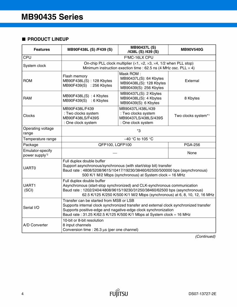
PRODUCT LINEUP
(Continued)
Features MB90F438L (S) /F439 (S) MB90437L (S) /438L (S) /439 (S) MB90V540G
CPU F2MC-16LX CPU
System clockOn-chip PLL clock multiplier (×1, ×2, ×3, ×4, 1/2 when PLL stop)
Minimum instruction exection time : 62.5 ns (4 MHz osc. PLL × 4)
ROMFlash memoryMB90F438L(S) : 128 KbytesMB90F439(S) : 256 Kbytes
Mask ROM : MB90437L(S): 64 Kbytes MB90438L(S): 128 Kbytes MB90439(S): 256 Kbytes
External
RAMMB90F438L(S) : 4 KbytesMB90F439(S) : 6 Kbytes
MB90437L(S): 2 Kbytes MB90438L(S): 4 Kbytes MB90439(S): 6 Kbytes
8 Kbytes
Clocks
MB90F438L/F439 : Two clocks systemMB90F438LS/F439S : One clock system
MB90437L/438L/439 : Two clocks systemMB90437LS/438LS/439S : One clock system
Two clocks system*1
Operating voltage range
*3
Temperature range −40 °C to 105 °CPackage QFP100, LQFP100 PGA-256
Emulator-specifypower supply*2 ⎯ None
UART0
Full duplex double bufferSupport asynchronous/synchronous (with start/stop bit) transferBaud rate : 4808/5208/9615/10417/19230/38460/62500/500000 bps (asynchronous)
500 K/1 M/2 Mbps (synchronous) at System clock = 16 MHz
UART1 (SCI)
Full duplex double bufferAsynchronous (start-stop synchronized) and CLK-synchronous communicationBaud rate : 1202/2404/4808/9615/19230/31250/38460/62500 bps (asynchronous)
62.5 K/125 K/250 K/500 K/1 M/2 Mbps (synchronous) at 6, 8, 10, 12, 16 MHz
Serial I/O
Transfer can be started from MSB or LSBSupports internal clock synchronized transfer and external clock synchronized transferSupports positive-edge and nagative-edge clock synchronizationBaud rate : 31.25 K/62.5 K/125 K/500 K/1 Mbps at System clock = 16 MHz
A/D Converter10-bit or 8-bit resolution8 input channelsConversion time : 26.3 µs (per one channel)
4 DS07-13727-2E
MB90435 Series
(Continued)
*1 : If the one clock system is used, equip X0A and X1A with clocks from the tool side.*2 : It is setting of DIP switch S2 when Emulator pod (MB2145-507) is used.Please refer to the MB2145-507 hardware
manual (2.7 Emulator-specific Power Pin) about details.*3 : OPERATING VOLTAGE RANGE
Features MB90F438L (S) /F439 (S) MB90437L (S) /438L (S) /439 (S) MB90V540G
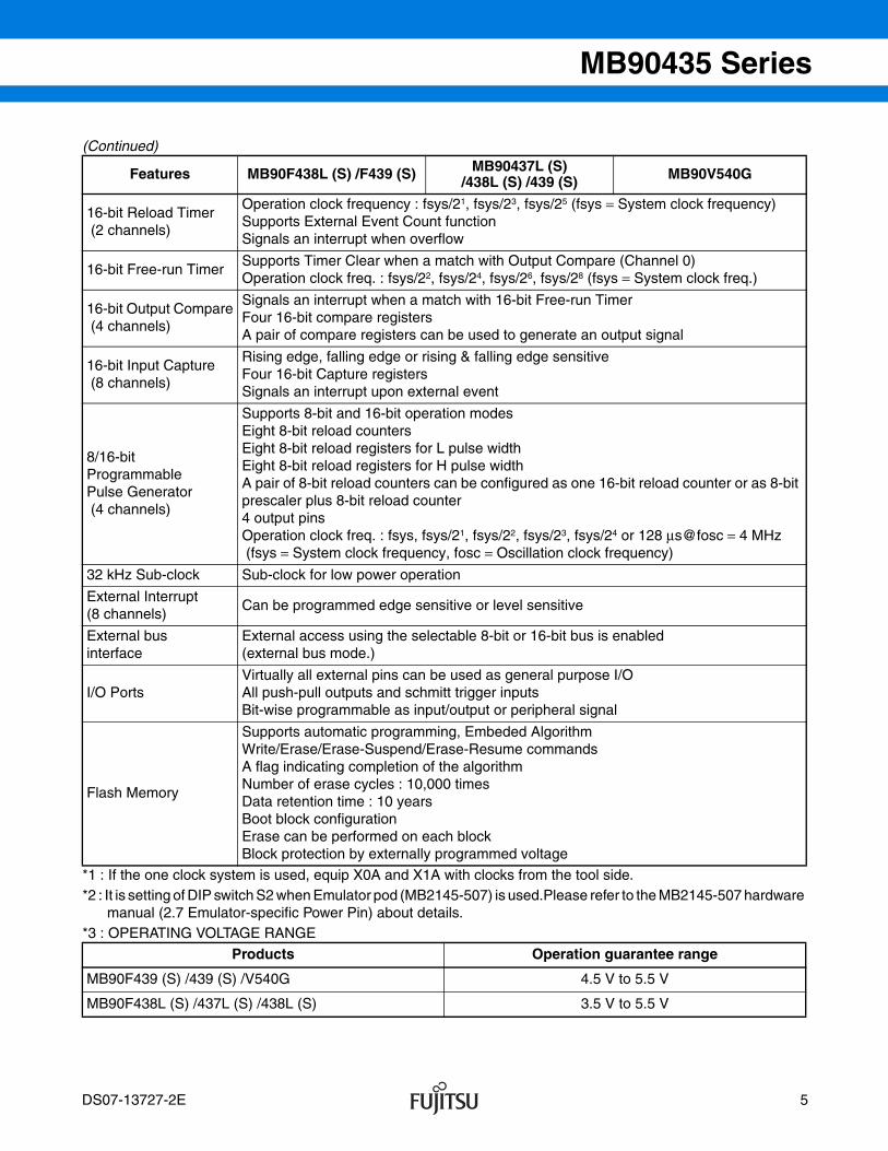
16-bit Reload Timer (2 channels)
Operation clock frequency : fsys/21, fsys/23, fsys/25 (fsys = System clock frequency) Supports External Event Count functionSignals an interrupt when overflow
16-bit Free-run TimerSupports Timer Clear when a match with Output Compare (Channel 0) Operation clock freq. : fsys/22, fsys/24, fsys/26, fsys/28 (fsys = System clock freq.)
16-bit Output Compare (4 channels)
Signals an interrupt when a match with 16-bit Free-run TimerFour 16-bit compare registersA pair of compare registers can be used to generate an output signal
16-bit Input Capture (8 channels)
Rising edge, falling edge or rising & falling edge sensitiveFour 16-bit Capture registersSignals an interrupt upon external event
8/16-bitProgrammablePulse Generator (4 channels)
Supports 8-bit and 16-bit operation modesEight 8-bit reload countersEight 8-bit reload registers for L pulse widthEight 8-bit reload registers for H pulse widthA pair of 8-bit reload counters can be configured as one 16-bit reload counter or as 8-bit prescaler plus 8-bit reload counter4 output pinsOperation clock freq. : fsys, fsys/21, fsys/22, fsys/23, fsys/24 or 128 µs@fosc = 4 MHz (fsys = System clock frequency, fosc = Oscillation clock frequency)
32 kHz Sub-clock Sub-clock for low power operation
External Interrupt(8 channels)
Can be programmed edge sensitive or level sensitive
External businterface
External access using the selectable 8-bit or 16-bit bus is enabled(external bus mode.)
I/O PortsVirtually all external pins can be used as general purpose I/OAll push-pull outputs and schmitt trigger inputsBit-wise programmable as input/output or peripheral signal
Flash Memory
Supports automatic programming, Embeded AlgorithmWrite/Erase/Erase-Suspend/Erase-Resume commandsA flag indicating completion of the algorithmNumber of erase cycles : 10,000 timesData retention time : 10 yearsBoot block configurationErase can be performed on each blockBlock protection by externally programmed voltage
Products Operation guarantee range
MB90F439 (S) /439 (S) /V540G 4.5 V to 5.5 V
MB90F438L (S) /437L (S) /438L (S) 3.5 V to 5.5 V
DS07-13727-2E 5
MB90435 Series
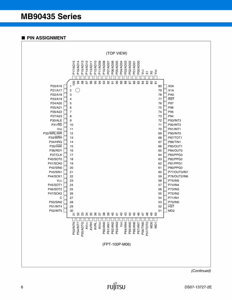
PIN ASSIGNMENT
(Continued)
(TOP VIEW)
(FPT-100P-M06)
123456789101112131415161718192021222324252627282930
X0AX1APA0RSTP97P96P95P94P93/INT3P92/INT2P91/INT1P90/INT0P87/TOT1P86/TIN1P85/OUT1P84/OUT0P83/PPG3P82/PPG2P81/PPG1P80/PPG0P77/OUT3/IN7P76/OUT2/IN6P75/IN5P74/IN4P73/IN3P72/IN2P71/IN1P70/IN0HSTMD2
807978777675747372717069686766656463626160595857565554535251
P20/A16P21/A17P22/A18P23/A19P24/A20P25/A21P26/A22P27/A23P30/ALEP31/RD
VSS
P32/WRL/WRP33/WRHP34/HRQP35/HAKP36/RDYP37/CLK
P40/SOT0P41/SCK0P42/SIN0P43/SIN1
P44/SCK1VCC
P45/SOT1P46/SOT2P47/SCK2
CP50/SIN2P51/INT4P52/INT5
100 99 98 97 96 95 94 93 92 91 90 89 88 87 86 85 84 83 82 81
P53
/INT
6P
54/IN
T7
P55
/AD
TG
AV
CC
AV
RH
AV
RL
AV
SS
P60
/AN
0P
61/A
N1
P62
/AN
2P
63/A
N3
VS
S
P64
/AN
4P
65/A
N5
P66
/AN
6P
67/A
N7
P56
/TIN
0P
57/T
OT
0M
D0
MD
1
31 32 33 34 35 36 37 38 39 40 41 42 43 44 45 46 47 48 49 50
P17
/AD
15P
16/A
D14
P15
/AD
13P
14/A
D12
P13
/AD
11P
12/A
D10
P11
/AD
09P
10/A
D08
P07
/AD
07P
06/A
D06
P05
/AD
05P
04/A
D04
P03
/AD
03P
02/A
D02
P01
/AD
01P
00/A
D00
VC
C
X1
X0
VS
S
6 DS07-13727-2E
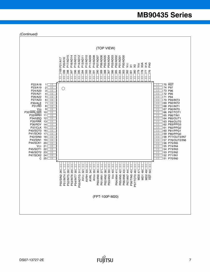
MB90435 Series
(Continued)
(TOP VIEW)
(FPT-100P-M20)
P22/A18P23/A19P24/A20P25/A21P26/A22P27/A23P30/ALEP31/RD
VSS
P32/WRL/WR
P34/HRQP33/WRH
P35/HAKP36/RDYP37/CLK
P40/SOT0P41/SCK0P42/SIN0P43/SIN1
P44/SCK1VCC
P45/SOT1P46/SOT2P47/SCK2
C
123456789
10111213141516171819202122232425
75747372717069686766656463626160595857565554535251
RSTP97P96P95P94P93/INT3P92/INT2P91/INT1P90/INT0P87/TOT1P86/TIN1P85/OUT1P84/OUT0P83/PPG3P82/PPG2P81/PPG1P80/PPG0P77/OUT3/IN7P76/OUT2/IN6P75/IN5P74/IN4P73/IN3P72/IN2P71/IN1P70/IN0
100
99 98 97 96 95 94 93 92 91 90 89 88 87 86 85 84 83 82 81 80 79 78 77 76
P21
/A17
P20
/A16
P17
/AD
15P
16/A
D14
P15
/AD
13P
14/A
D12
P13
/AD
11P
12/A
D10
P11
/AD
09P
10/A
D08
P07
/AD
07P
06/A
D06
P05
/AD
05P
04/A
D04
P03
/AD
03P
02/A
D02
P01
/AD
01P
00/A
D00
VC
C
X1
X0
VS
S
X0A
X1A
PA
0
26 27 28 29 30 31 32 33 34 35 36 37 38 39 40 41 42 43 44 45 46 47 48 49 50
P50
/SIN
2P
51/IN
T4
P52
/INT
5P
53/IN
T6
P54
/INT
7P
55/A
DT
GA
VC
C
AV
RH
AV
RL
AV
SS
P60
/AN
0P
61/A
N1
P62
/AN
2P
63/A
N3
VS
S
P64
/AN
4P
65/A
N5
P66
/AN
6P
67/A
N7
P56
/TIN
0P
57/T
OT
0M
D0
MD
1M
D2
HS
T
DS07-13727-2E 7
MB90435 Series
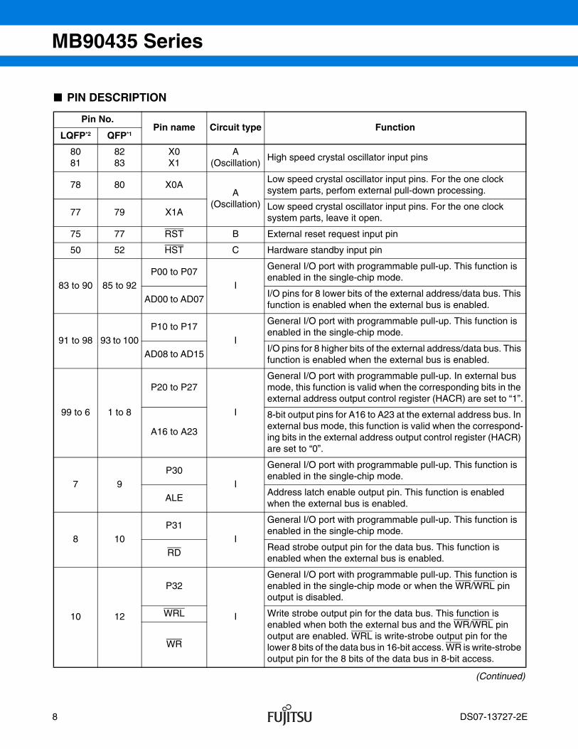
PIN DESCRIPTION
(Continued)
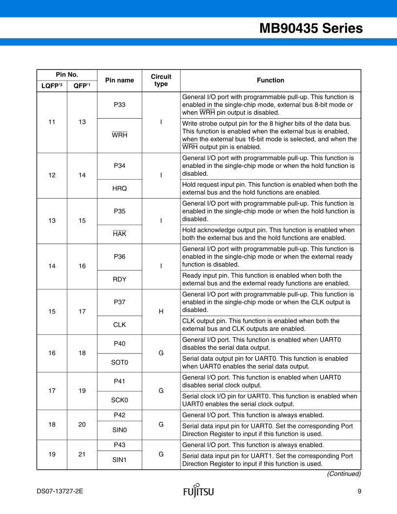
Pin No.Pin name Circuit type Function
LQFP*2 QFP*1
8081
8283
X0X1
A (Oscillation)
High speed crystal oscillator input pins
78 80 X0AA
(Oscillation)
Low speed crystal oscillator input pins. For the one clock system parts, perfom external pull-down processing.
77 79 X1ALow speed crystal oscillator input pins. For the one clock system parts, leave it open.
75 77 RST B External reset request input pin
50 52 HST C Hardware standby input pin
83 to 90 85 to 92
P00 to P07
I
General I/O port with programmable pull-up. This function is enabled in the single-chip mode.
AD00 to AD07I/O pins for 8 lower bits of the external address/data bus. This function is enabled when the external bus is enabled.
91 to 98 93 to 100
P10 to P17
I
General I/O port with programmable pull-up. This function is enabled in the single-chip mode.
AD08 to AD15I/O pins for 8 higher bits of the external address/data bus. This function is enabled when the external bus is enabled.
99 to 6 1 to 8
P20 to P27
I
General I/O port with programmable pull-up. In external bus mode, this function is valid when the corresponding bits in the external address output control register (HACR) are set to “1”.
A16 to A23
8-bit output pins for A16 to A23 at the external address bus. In external bus mode, this function is valid when the correspond-ing bits in the external address output control register (HACR) are set to “0”.
7 9
P30
I
General I/O port with programmable pull-up. This function is enabled in the single-chip mode.
ALEAddress latch enable output pin. This function is enabled when the external bus is enabled.
8 10
P31
I
General I/O port with programmable pull-up. This function is enabled in the single-chip mode.
RDRead strobe output pin for the data bus. This function is enabled when the external bus is enabled.
10 12
P32
I
General I/O port with programmable pull-up. This function is enabled in the single-chip mode or when the WR/WRL pin output is disabled.
WRL Write strobe output pin for the data bus. This function is enabled when both the external bus and the WR/WRL pin output are enabled. WRL is write-strobe output pin for the lower 8 bits of the data bus in 16-bit access. WR is write-strobe output pin for the 8 bits of the data bus in 8-bit access.
WR
8 DS07-13727-2E
MB90435 Series
(Continued)
Pin No.Pin name Circuit
type FunctionLQFP*2 QFP*1
11 13
P33
I
General I/O port with programmable pull-up. This function is enabled in the single-chip mode, external bus 8-bit mode or when WRH pin output is disabled.
WRH
Write strobe output pin for the 8 higher bits of the data bus. This function is enabled when the external bus is enabled, when the external bus 16-bit mode is selected, and when the WRH output pin is enabled.
12 14
P34
I
General I/O port with programmable pull-up. This function is enabled in the single-chip mode or when the hold function is disabled.
HRQHold request input pin. This function is enabled when both the external bus and the hold functions are enabled.
13 15
P35
I
General I/O port with programmable pull-up. This function is enabled in the single-chip mode or when the hold function is disabled.
HAKHold acknowledge output pin. This function is enabled when both the external bus and the hold functions are enabled.
14 16
P36
I
General I/O port with programmable pull-up. This function is enabled in the single-chip mode or when the external ready function is disabled.
RDYReady input pin. This function is enabled when both the external bus and the external ready functions are enabled.
15 17
P37
H
General I/O port with programmable pull-up. This function is enabled in the single-chip mode or when the CLK output is disabled.
CLKCLK output pin. This function is enabled when both the external bus and CLK outputs are enabled.
16 18
P40
G
General I/O port. This function is enabled when UART0 disables the serial data output.
SOT0Serial data output pin for UART0. This function is enabled when UART0 enables the serial data output.
17 19
P41
G
General I/O port. This function is enabled when UART0 disables serial clock output.
SCK0Serial clock I/O pin for UART0. This function is enabled when UART0 enables the serial clock output.
18 20
P42
G
General I/O port. This function is always enabled.
SIN0Serial data input pin for UART0. Set the corresponding Port Direction Register to input if this function is used.
19 21
P43
G
General I/O port. This function is always enabled.
SIN1Serial data input pin for UART1. Set the corresponding Port Direction Register to input if this function is used.
DS07-13727-2E 9
MB90435 Series
(Continued)
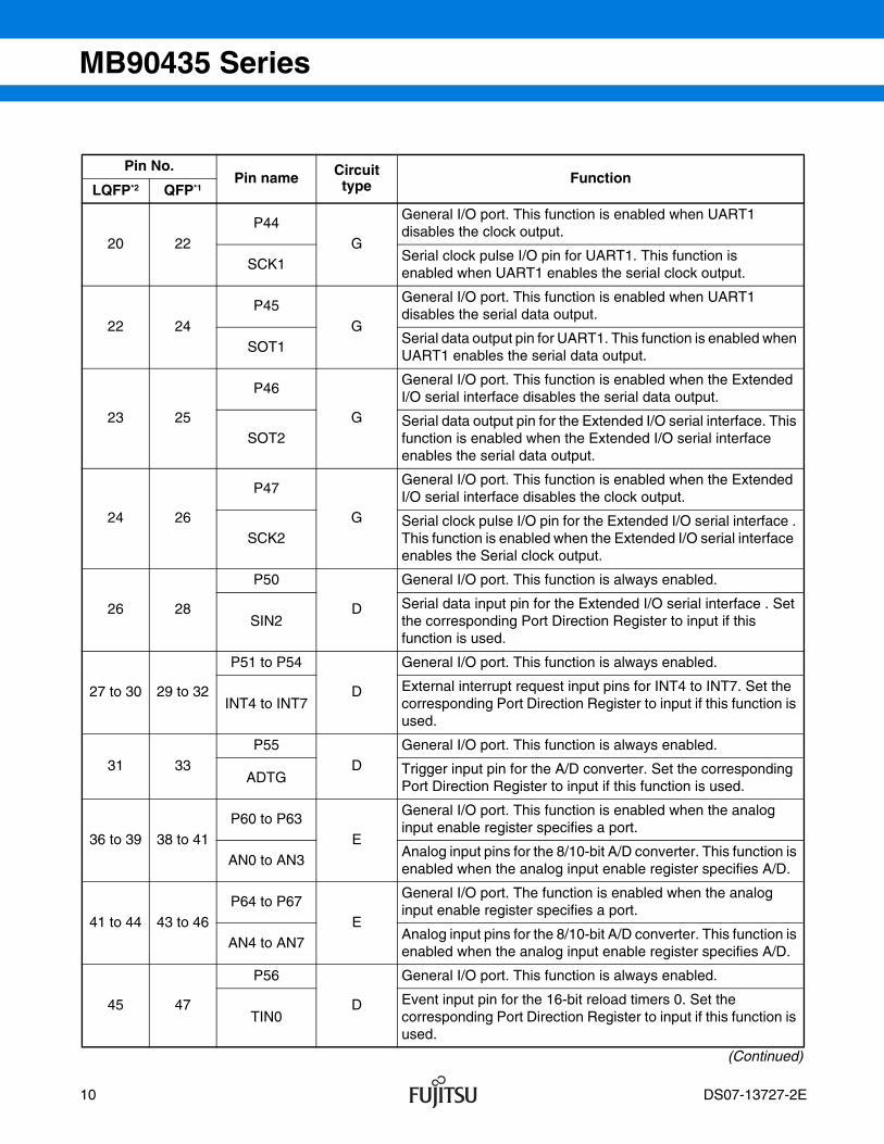
Pin No.Pin name Circuit
type FunctionLQFP*2 QFP*1
20 22P44
G
General I/O port. This function is enabled when UART1 disables the clock output.
SCK1Serial clock pulse I/O pin for UART1. This function is enabled when UART1 enables the serial clock output.
22 24P45
G
General I/O port. This function is enabled when UART1 disables the serial data output.
SOT1Serial data output pin for UART1. This function is enabled when UART1 enables the serial data output.
23 25
P46
G
General I/O port. This function is enabled when the Extended I/O serial interface disables the serial data output.
SOT2Serial data output pin for the Extended I/O serial interface. This function is enabled when the Extended I/O serial interface enables the serial data output.
24 26
P47
G
General I/O port. This function is enabled when the Extended I/O serial interface disables the clock output.
SCK2Serial clock pulse I/O pin for the Extended I/O serial interface . This function is enabled when the Extended I/O serial interface enables the Serial clock output.
26 28
P50
D
General I/O port. This function is always enabled.
SIN2Serial data input pin for the Extended I/O serial interface . Set the corresponding Port Direction Register to input if this function is used.
27 to 30 29 to 32
P51 to P54
D
General I/O port. This function is always enabled.
INT4 to INT7External interrupt request input pins for INT4 to INT7. Set the corresponding Port Direction Register to input if this function is used.
31 33P55
DGeneral I/O port. This function is always enabled.
ADTGTrigger input pin for the A/D converter. Set the corresponding Port Direction Register to input if this function is used.
36 to 39 38 to 41P60 to P63
E
General I/O port. This function is enabled when the analog input enable register specifies a port.
AN0 to AN3Analog input pins for the 8/10-bit A/D converter. This function is enabled when the analog input enable register specifies A/D.
41 to 44 43 to 46P64 to P67
E
General I/O port. The function is enabled when the analog input enable register specifies a port.
AN4 to AN7Analog input pins for the 8/10-bit A/D converter. This function is enabled when the analog input enable register specifies A/D.
45 47
P56
D
General I/O port. This function is always enabled.
TIN0Event input pin for the 16-bit reload timers 0. Set the corresponding Port Direction Register to input if this function is used.
10 DS07-13727-2E
MB90435 Series
(Continued)
Pin No.Pin name Circuit
type FunctionLQFP*2 QFP*1
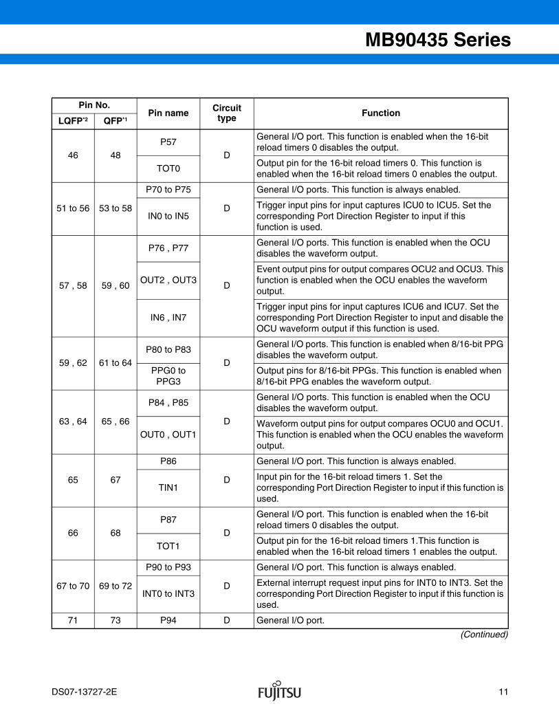
46 48
P57
D
General I/O port. This function is enabled when the 16-bit reload timers 0 disables the output.
TOT0Output pin for the 16-bit reload timers 0. This function is enabled when the 16-bit reload timers 0 enables the output.
51 to 56 53 to 58
P70 to P75
D
General I/O ports. This function is always enabled.
IN0 to IN5Trigger input pins for input captures ICU0 to ICU5. Set the corresponding Port Direction Register to input if this function is used.
57 , 58 59 , 60
P76 , P77
D
General I/O ports. This function is enabled when the OCU disables the waveform output.
OUT2 , OUT3Event output pins for output compares OCU2 and OCU3. This function is enabled when the OCU enables the waveform output.
IN6 , IN7Trigger input pins for input captures ICU6 and ICU7. Set the corresponding Port Direction Register to input and disable the OCU waveform output if this function is used.
59 , 62 61 to 64
P80 to P83
D
General I/O ports. This function is enabled when 8/16-bit PPG disables the waveform output.
PPG0 to PPG3
Output pins for 8/16-bit PPGs. This function is enabled when 8/16-bit PPG enables the waveform output.
63 , 64 65 , 66
P84 , P85
D
General I/O ports. This function is enabled when the OCU disables the waveform output.
OUT0 , OUT1Waveform output pins for output compares OCU0 and OCU1. This function is enabled when the OCU enables the waveform output.
65 67
P86
D
General I/O port. This function is always enabled.
TIN1Input pin for the 16-bit reload timers 1. Set the corresponding Port Direction Register to input if this function is used.
66 68
P87
D
General I/O port. This function is enabled when the 16-bit reload timers 0 disables the output.
TOT1Output pin for the 16-bit reload timers 1.This function is enabled when the 16-bit reload timers 1 enables the output.
67 to 70 69 to 72
P90 to P93
D
General I/O port. This function is always enabled.
INT0 to INT3External interrupt request input pins for INT0 to INT3. Set the corresponding Port Direction Register to input if this function is used.
71 73 P94 D General I/O port.
DS07-13727-2E 11
MB90435 Series
(Continued)
*1 : FPT-100P-M06
*2 : FPT-100P-M20
Pin No.Pin name Circuit
type FunctionLQFP*2 QFP*1
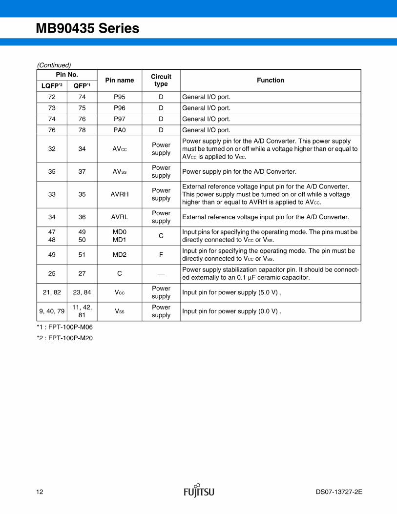
72 74 P95 D General I/O port.
73 75 P96 D General I/O port.
74 76 P97 D General I/O port.
76 78 PA0 D General I/O port.
32 34 AVCCPowersupply
Power supply pin for the A/D Converter. This power supply must be turned on or off while a voltage higher than or equal to AVCC is applied to VCC.
35 37 AVSSPowersupply
Power supply pin for the A/D Converter.
33 35 AVRHPowersupply
External reference voltage input pin for the A/D Converter. This power supply must be turned on or off while a voltage higher than or equal to AVRH is applied to AVCC.
34 36 AVRLPowersupply
External reference voltage input pin for the A/D Converter.
4748
4950
MD0MD1
CInput pins for specifying the operating mode. The pins must be directly connected to VCC or VSS.
49 51 MD2 FInput pin for specifying the operating mode. The pin must be directly connected to VCC or VSS.
25 27 C ⎯ Power supply stabilization capacitor pin. It should be connect-ed externally to an 0.1 µF ceramic capacitor.
21, 82 23, 84 VCCPowersupply
Input pin for power supply (5.0 V) .
9, 40, 7911, 42,
81VSS
Powersupply
Input pin for power supply (0.0 V) .
12 DS07-13727-2E
MB90435 Series
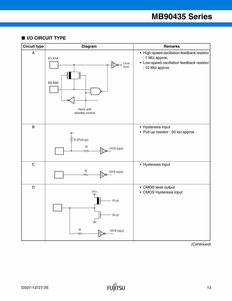
I/O CIRCUIT TYPE
(Continued)
Circuit type Diagram Remarks
A • High-speed oscillation feedback resistor: 1 MΩ approx.
• Low-speed oscillation feedback resistor: 10 MΩ approx.
B • Hysteresis input• Pull-up resistor : 50 kΩ approx.
C • Hysteresis input
D • CMOS level output• CMOS Hysteresis input
X1,X1A
X0,X0A
Hard, softstandby control
Clockinput
R
R (Pull-up)
HYS input
R HYS input
R
P-ch
N-ch
HYS input
VCC
DS07-13727-2E 13
MB90435 Series
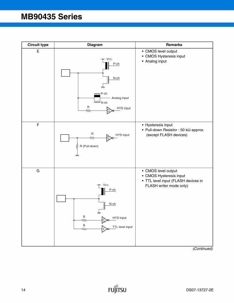
(Continued)
Circuit type Diagram Remarks
E • CMOS level output• CMOS Hysteresis input• Analog input
F • Hysteresis input • Pull-down Resistor : 50 kΩ approx.
(except FLASH devices)
G • CMOS level output• CMOS Hysteresis input• TTL level input (FLASH devices in
FLASH writer mode only)
R
VCC
P-ch
N-ch
HYS input
Analog inputP-ch
N-ch
R
R (Pull-down)
HYS input
R
VCC
P-ch
N-ch
RT
HYS input
TTL level input
14 DS07-13727-2E
MB90435 Series
(Continued)
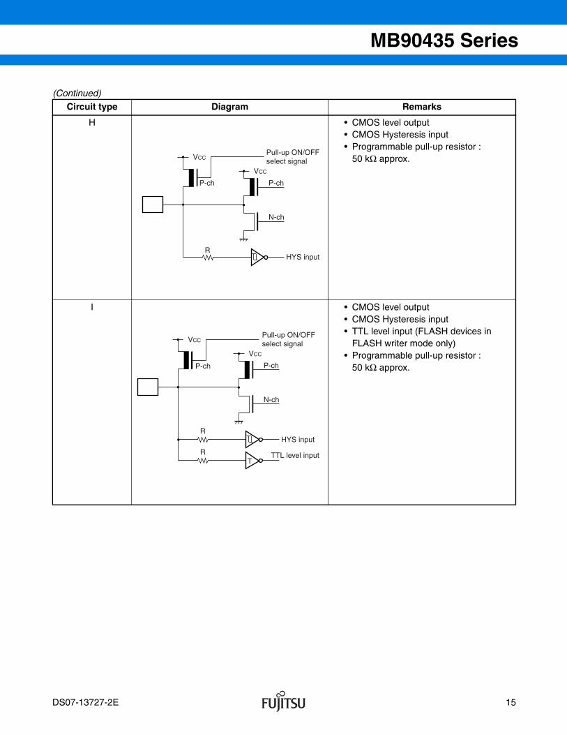
Circuit type Diagram Remarks
H • CMOS level output• CMOS Hysteresis input• Programmable pull-up resistor :
50 kΩ approx.
I • CMOS level output• CMOS Hysteresis input• TTL level input (FLASH devices in
FLASH writer mode only) • Programmable pull-up resistor :
50 kΩ approx.
VCC
P-chP-ch
N-ch
VCC
HYS input
Pull-up ON/OFFselect signal
R
R
VCC
P-chP-ch
N-ch
RT
VCCPull-up ON/OFF select signal
HYS input
TTL level input
DS07-13727-2E 15
MB90435 Series
HANDLING DEVICES (1) Preventing latch-up
CMOS IC chips may suffer latch-up under the following conditions : • A voltage higher than VCC or lower than VSS is applied to an input or output pin.• A voltage higher than the rated voltage is applied between VCC and VSS.• The AVcc power supply is applied before the VCC voltage.
Latch-up may increase the power supply current drastically, causing thermal damage to the device.For the same reason, care must also be taken in not allowing the analog power-supply voltage (AVCC, AVRH) toexceed the digital power-supply voltage.
(2) Handling unused pins
Leaving unused input pins open may result in misbehavior or latch up and possible permanent damage of thedevice. Therefor they must be pulled up or pulled down through resistors. In this case those resistors should bemore than 2 kΩ.Unused bi-directional pins should be set to the output state and can be left open, or the input state with theabove described connection.
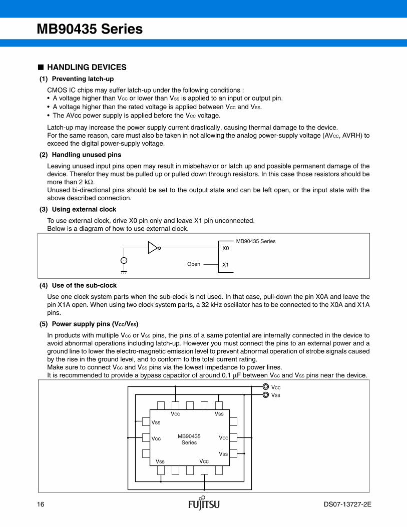
(3) Using external clock
To use external clock, drive X0 pin only and leave X1 pin unconnected.Below is a diagram of how to use external clock.
(4) Use of the sub-clock
Use one clock system parts when the sub-clock is not used. In that case, pull-down the pin X0A and leave thepin X1A open. When using two clock system parts, a 32 kHz oscillator has to be connected to the X0A and X1Apins.
(5) Power supply pins (VCC/VSS)
In products with multiple VCC or VSS pins, the pins of a same potential are internally connected in the device toavoid abnormal operations including latch-up. However you must connect the pins to an external power and aground line to lower the electro-magnetic emission level to prevent abnormal operation of strobe signals causedby the rise in the ground level, and to conform to the total current rating.Make sure to connect VCC and VSS pins via the lowest impedance to power lines.It is recommended to provide a bypass capacitor of around 0.1 µF between VCC and VSS pins near the device.
X0
X1
MB90435 Series
Open
VCC
VCCVCC
VCC
VCC
VSS
VSS
VSS
VSS
VSS
MB90435Series
16 DS07-13727-2E
MB90435 Series
(6) Pull-up/down resistors
The MB90435 Series does not support internal pull-up/down resistors (except Port0 − Port3 : pull-up resistors) . Use external components where needed.
(7) Crystal Oscillator Circuit
Noises around X0 or X1 pins may be possible causes of abnormal operations. Make sure to provide bypasscapacitors via the shortest distances from X0, X1 pins, crystal oscillator (or ceramic resonator) and ground lines,and make sure, to the utmost effort, that lines of oscillation circuits do not cross the lines of other circuits.It is highly recommended to provide a printed circuit board artwork surrounding X0 and X1 pins with a groundarea for stabilizing the operation.
(8) Turning-on Sequence of Power Supply to A/D Converter and Analog Inputs
Make sure to turn on the A/D converter power supply (AVCC, AVRH, AVRL) and analog inputs (AN0 to AN7) afterturning-on the digital power supply (VCC) .Turn-off the digital power after turning off the A/D converter supply and analog inputs. In this case, make surethat the voltage does not exceed AVRH or AVCC (turning on/off the analog and digital power supplies simulta-neously is acceptable) .
(9) Connection of Unused Pins of A/D Converter
Connect unused pins of A/D converter to AVCC = VCC, AVSS = AVRH = VSS.
(10) N.C. Pin
The N.C. (internally connected) pin must be opened for use.
(11) Notes on Energization
To prevent the internal regulator circuit from malfunctioning, set the voltage rise time during energization at 50 µs or more (0.2 V to 2.7 V) .
(12) Initialization
In the device, there are internal registers which are initialized only by a power-on reset. To initialize these registers,please turn on the power again.
(13) Directions of “DIV A, Ri” and “DIVW A, RWi” instructions
In the Signed multiplication and division instructions (“DIV A, Ri” and “DIVW A, RWi”) , the value of the corresponding bank register (DTB, ADB, USB, SSB) is set in “00H”.
If the values of the corresponding bank registers (DTB, ADB, USB, SSB) are set to other than “00H”, the remainderby the execution result of the instruction is not stored in the register of the instruction operand.
(14) Using REALOS
The use of EI2OS is not possible with the REALOS real time operating system.
(15) Caution on Operations during PLL Clock Mode
If the PLL clock mode is selected, the microcontroller attempt to be working with the self-oscillating circuit evenwhen there is no external oscillator or external clock input is stopped. Performance of this operation, however,cannot be guaranteed.
DS07-13727-2E 17
MB90435 Series
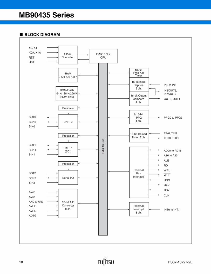
BLOCK DIAGRAM
X0, X1
SOT0
SCK0
SIN0
SOT1
SCK1
SIN1
SOT2
SCK2
SIN2
AVCC
AVSS
AN0 to AN7
AVRH
AVRL
ADTG
X0A, X1A
RST
HST
F2MC 16LXCPU
FM
C-1
6 B
us
IN0 to IN5
IN6/OUT2,IN7/OUT3
OUT0, OUT1
TIN0, TIN1
AD00 to AD15
A16 to A23
ALE
RD
WRL
WRH
HRQ
HAK
RDY
CLK
INT0 to INT7
TOT0, TOT1
PPG0 to PPG3
ClockController
RAM2 K/4 K/6 K/8 K
ROM/Flash64K/128 K/256 K
(ROM only)
Prescaler
UART0
UART1(SCI)
Prescaler
Serial I/O
10-bit A/DConverter
8 ch.
Prescaler
16-bit Free-run
Timer
16-bit InputCapture
8 ch.
16-bit OutputCompare
4 ch.
8/16-bit PPG4 ch.
16-bit ReloadTimer 2 ch.
ExternalBus
Interface
ExternalInterrupt
8 ch.
18 DS07-13727-2E
MB90435 Series
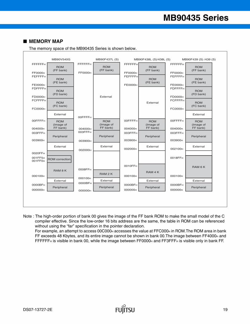
MEMORY MAPThe memory space of the MB90435 Series is shown below.
Note : The high-order portion of bank 00 gives the image of the FF bank ROM to make the small model of the C compiler effective. Since the low-order 16 bits address are the same, the table in ROM can be referenced without using the “far” specification in the pointer declaration.For example, an attempt to access 00C000H accesses the value at FFC000H in ROM.The ROM area in bank FF exceeds 48 Kbytes, and its entire image cannot be shown in bank 00.The image between FF4000H and FFFFFFH is visible in bank 00, while the image between FF0000H and FF3FFFH is visible only in bank FF.
MB90V540G
FFFFFFH
FEFFFFH
FF0000H
FDFFFFH
FE0000H
FCFFFFH
FD0000H
00FFFFH
004000H
003FFFH
003900H
0020FFH
001FF5H
001FF0H
000100H
0000BFH
000000H
FC0000H
ROM(FF bank)
ROM(FE bank)
ROM(FD bank)
ROM(FC bank)
External
ROM(Image ofFF bank)
Peripheral
External
RAM 8 K
External
Peripheral
ROM correction
MB90F438L (S)/438L (S)
FFFFFFH
FEFFFFH
FF0000H
FE0000H
00FFFFH
004000H
003FFFH
003900H
002000H
0010FFH
000100H
0000BFH
000000H
ROM(FF bank)
ROM(FE bank)
External
ROM(Image ofFF bank)
Peripheral
External
RAM 4 K
External
Peripheral
MB90F439 (S) /439 (S)
FDFFFFH
FCFFFFH
FD0000H
FC0000H
ROM(FD bank)
ROM(FC bank)
FFFFFFH
FEFFFFH
FF0000H
FE0000H
00FFFFH
004000H
003FFFH
003900H
002100H
0018FFH
000100H
0000BFH
000000H
ROM(FF bank)
ROM(FE bank)
External
ROM(Image ofFF bank)
Peripheral
External
RAM 6 K
External
Peripheral
FFFFFFH
FF0000H
00FFFFH
004000H
003FFFH
003900H
002000H
0008FFH
000100H
0000BFH
ROM(FF bank)
ROM(Image ofFF bank)
Peripheral
External
RAM 2 K
External
Peripheral
MB90F437L (S)
000000H
External
DS07-13727-2E 19
asatani
ノート
asatani : Marked
asatani
ノート
asatani : Marked
asatani
ノート
asatani : Marked
MB90435 Series
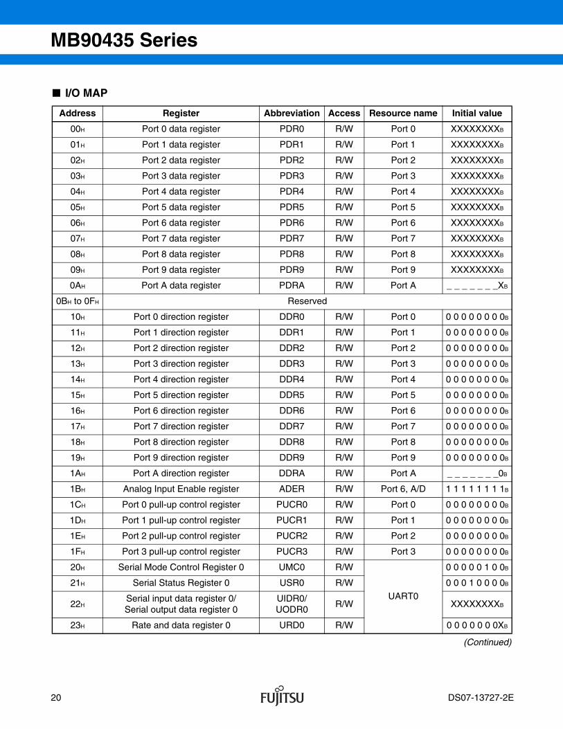
I/O MAP
(Continued)
Address Register Abbreviation Access Resource name Initial value
00H Port 0 data register PDR0 R/W Port 0 XXXXXXXXB
01H Port 1 data register PDR1 R/W Port 1 XXXXXXXXB
02H Port 2 data register PDR2 R/W Port 2 XXXXXXXXB
03H Port 3 data register PDR3 R/W Port 3 XXXXXXXXB
04H Port 4 data register PDR4 R/W Port 4 XXXXXXXXB
05H Port 5 data register PDR5 R/W Port 5 XXXXXXXXB
06H Port 6 data register PDR6 R/W Port 6 XXXXXXXXB
07H Port 7 data register PDR7 R/W Port 7 XXXXXXXXB
08H Port 8 data register PDR8 R/W Port 8 XXXXXXXXB
09H Port 9 data register PDR9 R/W Port 9 XXXXXXXXB
0AH Port A data register PDRA R/W Port A _ _ _ _ _ _ _XB
0BH to 0FH Reserved
10H Port 0 direction register DDR0 R/W Port 0 0 0 0 0 0 0 0 0B
11H Port 1 direction register DDR1 R/W Port 1 0 0 0 0 0 0 0 0B
12H Port 2 direction register DDR2 R/W Port 2 0 0 0 0 0 0 0 0B
13H Port 3 direction register DDR3 R/W Port 3 0 0 0 0 0 0 0 0B
14H Port 4 direction register DDR4 R/W Port 4 0 0 0 0 0 0 0 0B
15H Port 5 direction register DDR5 R/W Port 5 0 0 0 0 0 0 0 0B
16H Port 6 direction register DDR6 R/W Port 6 0 0 0 0 0 0 0 0B
17H Port 7 direction register DDR7 R/W Port 7 0 0 0 0 0 0 0 0B
18H Port 8 direction register DDR8 R/W Port 8 0 0 0 0 0 0 0 0B
19H Port 9 direction register DDR9 R/W Port 9 0 0 0 0 0 0 0 0B
1AH Port A direction register DDRA R/W Port A _ _ _ _ _ _ _0B
1BH Analog Input Enable register ADER R/W Port 6, A/D 1 1 1 1 1 1 1 1B
1CH Port 0 pull-up control register PUCR0 R/W Port 0 0 0 0 0 0 0 0 0B
1DH Port 1 pull-up control register PUCR1 R/W Port 1 0 0 0 0 0 0 0 0B
1EH Port 2 pull-up control register PUCR2 R/W Port 2 0 0 0 0 0 0 0 0B
1FH Port 3 pull-up control register PUCR3 R/W Port 3 0 0 0 0 0 0 0 0B
20H Serial Mode Control Register 0 UMC0 R/W
UART0
0 0 0 0 0 1 0 0B
21H Serial Status Register 0 USR0 R/W 0 0 0 1 0 0 0 0B
22HSerial input data register 0/Serial output data register 0
UIDR0/UODR0
R/W XXXXXXXXB
23H Rate and data register 0 URD0 R/W 0 0 0 0 0 0 0XB
20 DS07-13727-2E
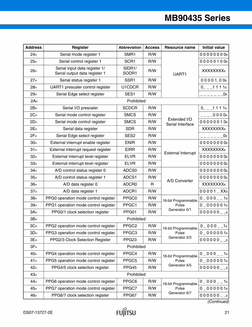
MB90435 Series
(Continued)
Address Register Abbreviation Access Resource name Initial value
24H Serial mode register 1 SMR1 R/W
UART1
0 0 0 0 0 0 0 0B
25H Serial control register 1 SCR1 R/W 0 0 0 0 0 1 0 0B
26HSerial input data register 1/Serial output data register 1
SIDR1/SODR1
R/W XXXXXXXXB
27H Serial status register 1 SSR1 R/W 0 0 0 0 1_0 0B
28H UART1 prescaler control register U1CDCR R/W 0_ _ _1 1 1 1B
29H Serial Edge select register SES1 R/W _ _ _ _ _ _ _0B
2AH Prohibited
2BH Serial I/O prescaler SCDCR R/W
Extended I/O Serial Interface
0_ _ _1 1 1 1B
2CH Serial mode control register SMCS R/W _ _ _ _0 0 0 0B
2DH Serial mode control register SMCS R/W 0 0 0 0 0 0 1 0B
2EH Serial data register SDR R/W XXXXXXXXB
2FH Serial Edge select register SES2 R/W _ _ _ _ _ _ _0B
30H External interrupt enable register ENIR R/W
External Interrupt
0 0 0 0 0 0 0 0B
31H External interrupt request register EIRR R/W XXXXXXXXB
32H External interrupt level register ELVR R/W 0 0 0 0 0 0 0 0B
33H External interrupt level register ELVR R/W 0 0 0 0 0 0 0 0B
34H A/D control status register 0 ADCS0 R/W
A/D Converter
0 0 0 0 0 0 0 0B
35H A/D control status register 1 ADCS1 R/W 0 0 0 0 0 0 0 0B
36H A/D data register 0 ADCR0 R XXXXXXXXB
37H A/D data register 1 ADCR1 R/W 0 0 0 0 1 _ XXB
38H PPG0 operation mode control register PPGC0 R/W16-bit Programmable
Pulse Generator 0/1
0 _ 0 0 0 _ _ 1B
39H PPG1 operation mode control register PPGC1 R/W 0 _ 0 0 0 0 0 1B
3AH PPG0/1 clock selection register PPG01 R/W 0 0 0 0 0 0 _ _B
3BH Prohibited
3CH PPG2 operation mode control register PPGC2 R/W16-bit Programmable
Pulse Generator 2/3
0 _ 0 0 0 _ _1B
3DH PPG3 operation mode control register PPGC3 R/W 0 _ 0 0 0 0 0 1B
3EH PPG2/3 Clock Selection Register PPG23 R/W 0 0 0 0 0 0 _ _B
3FH Prohibited
40H PPG4 operation mode control register PPGC4 R/W16-bit Programmable
Pulse Generator 4/5
0 _ 0 0 0 _ _ 1B
41H PPG5 operation mode control register PPGC5 R/W 0 _ 0 0 0 0 0 1B
42H PPG4/5 clock selection register PPG45 R/W 0 0 0 0 0 0 _ _B
43H Prohibited
44H PPG6 operation mode control register PPGC6 R/W16-bit Programmable
Pulse Generator 6/7
0 _ 0 0 0 _ _ 1B
45H PPG7 operation mode control register PPGC7 R/W 0 _ 0 0 0 0 0 1B
46H PPG6/7 clock selection register PPG67 R/W 0 0 0 0 0 0 _ _B
DS07-13727-2E 21
MB90435 Series
(Continued)
Address Register Abbreviation Access Resource name Initial value
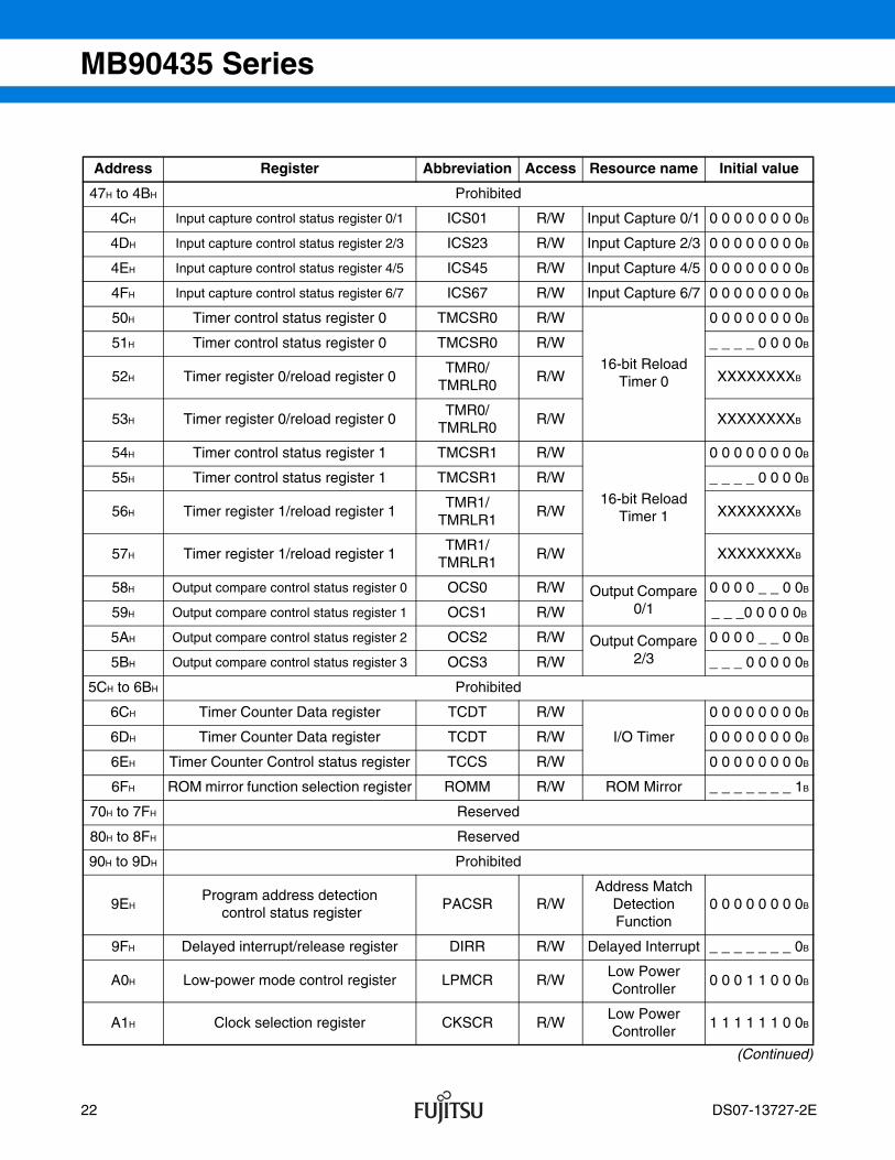
47H to 4BH Prohibited
4CH Input capture control status register 0/1 ICS01 R/W Input Capture 0/1 0 0 0 0 0 0 0 0B
4DH Input capture control status register 2/3 ICS23 R/W Input Capture 2/3 0 0 0 0 0 0 0 0B
4EH Input capture control status register 4/5 ICS45 R/W Input Capture 4/5 0 0 0 0 0 0 0 0B
4FH Input capture control status register 6/7 ICS67 R/W Input Capture 6/7 0 0 0 0 0 0 0 0B
50H Timer control status register 0 TMCSR0 R/W
16-bit Reload Timer 0
0 0 0 0 0 0 0 0B
51H Timer control status register 0 TMCSR0 R/W _ _ _ _ 0 0 0 0B
52H Timer register 0/reload register 0TMR0/
TMRLR0R/W XXXXXXXXB
53H Timer register 0/reload register 0TMR0/
TMRLR0R/W XXXXXXXXB
54H Timer control status register 1 TMCSR1 R/W
16-bit Reload Timer 1
0 0 0 0 0 0 0 0B
55H Timer control status register 1 TMCSR1 R/W _ _ _ _ 0 0 0 0B
56H Timer register 1/reload register 1TMR1/
TMRLR1R/W XXXXXXXXB
57H Timer register 1/reload register 1TMR1/
TMRLR1R/W XXXXXXXXB
58H Output compare control status register 0 OCS0 R/W Output Compare 0/1
0 0 0 0 _ _ 0 0B
59H Output compare control status register 1 OCS1 R/W _ _ _0 0 0 0 0B
5AH Output compare control status register 2 OCS2 R/W Output Compare 2/3
0 0 0 0 _ _ 0 0B
5BH Output compare control status register 3 OCS3 R/W _ _ _ 0 0 0 0 0B
5CH to 6BH Prohibited
6CH Timer Counter Data register TCDT R/W
I/O Timer
0 0 0 0 0 0 0 0B
6DH Timer Counter Data register TCDT R/W 0 0 0 0 0 0 0 0B
6EH Timer Counter Control status register TCCS R/W 0 0 0 0 0 0 0 0B
6FH ROM mirror function selection register ROMM R/W ROM Mirror _ _ _ _ _ _ _ 1B
70H to 7FH Reserved
80H to 8FH Reserved
90H to 9DH Prohibited
9EHProgram address detection
control status registerPACSR R/W
Address MatchDetectionFunction
0 0 0 0 0 0 0 0B
9FH Delayed interrupt/release register DIRR R/W Delayed Interrupt _ _ _ _ _ _ _ 0B
A0H Low-power mode control register LPMCR R/WLow PowerController
0 0 0 1 1 0 0 0B
A1H Clock selection register CKSCR R/WLow PowerController
1 1 1 1 1 1 0 0B
22 DS07-13727-2E
MB90435 Series
(Continued)
Address Register Abbreviation Access Resource name Initial value
A2H to A4H Prohibited
A5H Automatic ready function select register ARSR WExternal Memory
Access
0 0 1 1 _ _ 0 0B
A6H External address output control register HACR W 0 0 0 0 0 0 0 0B
A7H Bus control signal selection register ECSR W 0 0 0 0 0 0 0 _B
A8H Watchdog Timer control register WDTC R/W Watchdog Timer XXXXX 1 1 1B
A9H Time Base Timer Control register TBTC R/W Time Base Timer 1 - - 0 0 1 0 0B
AAH Watch timer control register WTC R/W Watch Timer 1 X 0 0 0 0 0 0B
ABH to ADH Prohibited
AEHFlash memory control status register
(Flash only, otherwise reserved) FMCS R/W Flash Memory 0 0 0 X 0 0 0 0B
AFH Prohibited
B0H Interrupt control register 00 ICR00 R/W
Interruptcontroller
0 0 0 0 0 1 1 1B
B1H Interrupt control register 01 ICR01 R/W 0 0 0 0 0 1 1 1B
B2H Interrupt control register 02 ICR02 R/W 0 0 0 0 0 1 1 1B
B3H Interrupt control register 03 ICR03 R/W 0 0 0 0 0 1 1 1B
B4H Interrupt control register 04 ICR04 R/W 0 0 0 0 0 1 1 1B
B5H Interrupt control register 05 ICR05 R/W 0 0 0 0 0 1 1 1B
B6H Interrupt control register 06 ICR06 R/W 0 0 0 0 0 1 1 1B
B7H Interrupt control register 07 ICR07 R/W 0 0 0 0 0 1 1 1B
B8H Interrupt control register 08 ICR08 R/W 0 0 0 0 0 1 1 1B
B9H Interrupt control register 09 ICR09 R/W 0 0 0 0 0 1 1 1B
BAH Interrupt control register 10 ICR10 R/W 0 0 0 0 0 1 1 1B
BBH Interrupt control register 11 ICR11 R/W 0 0 0 0 0 1 1 1B
BCH Interrupt control register 12 ICR12 R/W 0 0 0 0 0 1 1 1B
BDH Interrupt control register 13 ICR13 R/W 0 0 0 0 0 1 1 1B
BEH Interrupt control register 14 ICR14 R/W 0 0 0 0 0 1 1 1B
BFH Interrupt control register 15 ICR15 R/W 0 0 0 0 0 1 1 1B
C0H to FFH External
DS07-13727-2E 23
asatani
ノート
asatani : Marked
MB90435 Series
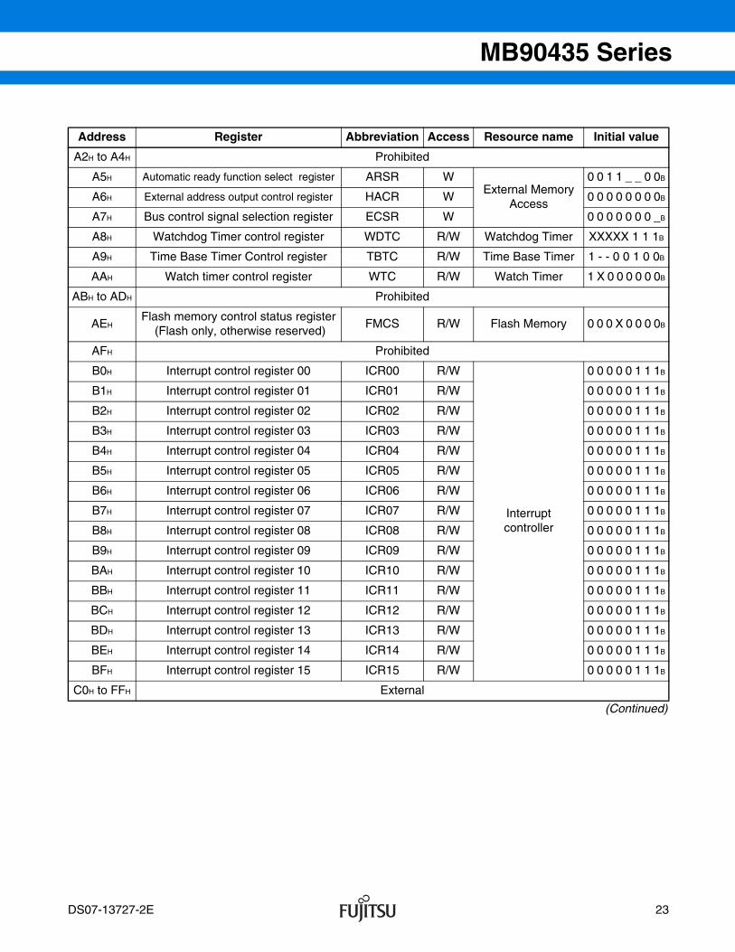
(Continued)
Address Register Abbreviation Access Resource name Initial value
1FF0HProgram address detec-
tion register 0PADR0 R/W
Address MatchDetection Function
XXXXXXXXB
1FF1HProgram address detec-
tion register 0PADR0 R/W XXXXXXXXB
1FF2HProgram address detec-
tion register 0PADR0 R/W XXXXXXXXB
1FF3HProgram address detec-
tion register 1PADR1 R/W XXXXXXXXB
1FF4HProgram address detec-
tion register 1PADR1 R/W XXXXXXXXB
1FF5HProgram address detec-
tion register 1PADR1 R/W XXXXXXXXB
3900H Reload L PRLL0 R/W
16-bit Programmable Pulse Generator 0/1
XXXXXXXXB
3901H Reload H PRLH0 R/W XXXXXXXXB
3902H Reload L PRLL1 R/W XXXXXXXXB
3903H Reload H PRLH1 R/W XXXXXXXXB
3904H Reload L PRLL2 R/W
16-bit Programmable Pulse Generator 2/3
XXXXXXXXB
3905H Reload H PRLH2 R/W XXXXXXXXB
3906H Reload L PRLL3 R/W XXXXXXXXB
3907H Reload H PRLH3 R/W XXXXXXXXB
3908H Reload L PRLL4 R/W
16-bit Programmable Pulse Generator 4/5
XXXXXXXXB
3909H Reload H PRLH4 R/W XXXXXXXXB
390AH Reload L PRLL5 R/W XXXXXXXXB
390BH Reload H PRLH5 R/W XXXXXXXXB
390CH Reload L PRLL6 R/W
16-bit Programmable Pulse Generator 6/7
XXXXXXXXB
390DH Reload H PRLH6 R/W XXXXXXXXB
390EH Reload L PRLL7 R/W XXXXXXXXB
390FH Reload H PRLH7 R/W XXXXXXXXB
3910H to 3917H
Reserved
3918H Input Capture Register 0 IPCP0 R
Input Capture 0/1
XXXXXXXXB
3919H Input Capture Register 0 IPCP0 R XXXXXXXXB
391AH Input Capture Register 1 IPCP1 R XXXXXXXXB
391BH Input Capture Register 1 IPCP1 R XXXXXXXXB
391CH Input Capture Register 2 IPCP2 R
Input Capture 2/3
XXXXXXXXB
391DH Input Capture Register 2 IPCP2 R XXXXXXXXB
391EH Input Capture Register 3 IPCP3 R XXXXXXXXB
391FH Input Capture Register 3 IPCP3 R XXXXXXXXB
24 DS07-13727-2E
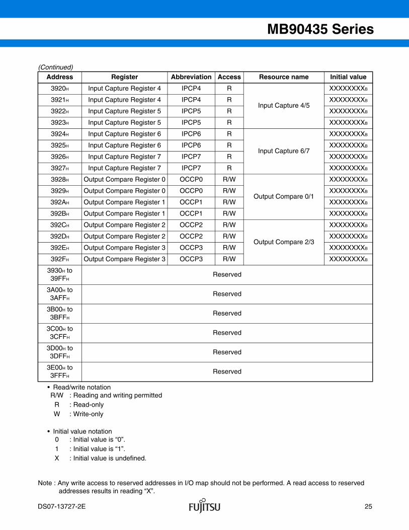
MB90435 Series
(Continued)
• Read/write notation
• Initial value notation
Note : Any write access to reserved addresses in I/O map should not be performed. A read access to reserved addresses results in reading “X”.
Address Register Abbreviation Access Resource name Initial value
3920H Input Capture Register 4 IPCP4 R
Input Capture 4/5
XXXXXXXXB
3921H Input Capture Register 4 IPCP4 R XXXXXXXXB
3922H Input Capture Register 5 IPCP5 R XXXXXXXXB
3923H Input Capture Register 5 IPCP5 R XXXXXXXXB
3924H Input Capture Register 6 IPCP6 R
Input Capture 6/7
XXXXXXXXB
3925H Input Capture Register 6 IPCP6 R XXXXXXXXB
3926H Input Capture Register 7 IPCP7 R XXXXXXXXB
3927H Input Capture Register 7 IPCP7 R XXXXXXXXB
3928H Output Compare Register 0 OCCP0 R/W
Output Compare 0/1
XXXXXXXXB
3929H Output Compare Register 0 OCCP0 R/W XXXXXXXXB
392AH Output Compare Register 1 OCCP1 R/W XXXXXXXXB
392BH Output Compare Register 1 OCCP1 R/W XXXXXXXXB
392CH Output Compare Register 2 OCCP2 R/W
Output Compare 2/3
XXXXXXXXB
392DH Output Compare Register 2 OCCP2 R/W XXXXXXXXB
392EH Output Compare Register 3 OCCP3 R/W XXXXXXXXB
392FH Output Compare Register 3 OCCP3 R/W XXXXXXXXB
3930H to 39FFH
Reserved
3A00H to 3AFFH
Reserved
3B00H to 3BFFH
Reserved
3C00H to 3CFFH
Reserved
3D00H to 3DFFH
Reserved
3E00H to 3FFFH
Reserved
R/W : Reading and writing permittedR : Read-onlyW : Write-only
0 : Initial value is “0”.1 : Initial value is “1”.X : Initial value is undefined.
DS07-13727-2E 25
MB90435 Series
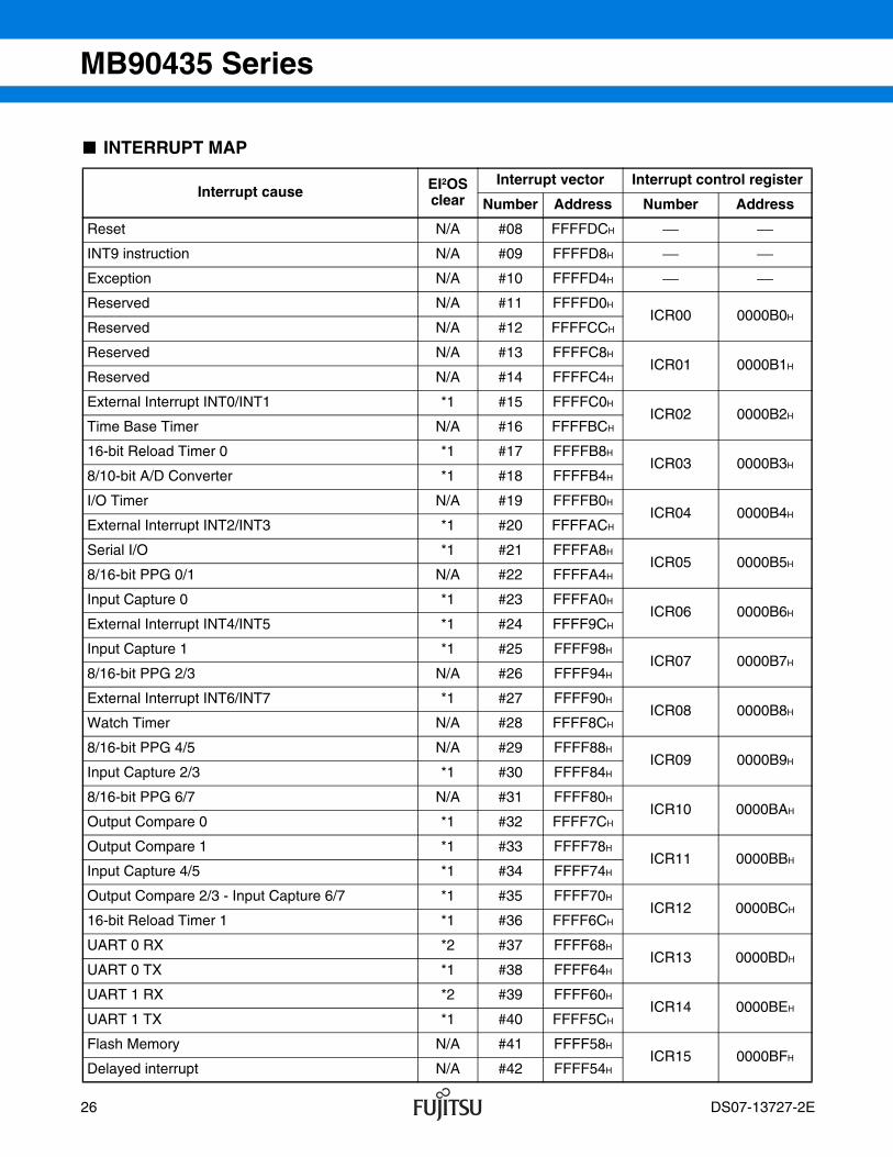
INTERRUPT MAP
Interrupt cause EI2OS clear
Interrupt vector Interrupt control register
Number Address Number Address
Reset N/A #08 FFFFDCH ⎯ ⎯
INT9 instruction N/A #09 FFFFD8H ⎯ ⎯
Exception N/A #10 FFFFD4H ⎯ ⎯
Reserved N/A #11 FFFFD0HICR00 0000B0H
Reserved N/A #12 FFFFCCH
Reserved N/A #13 FFFFC8HICR01 0000B1H
Reserved N/A #14 FFFFC4H
External Interrupt INT0/INT1 *1 #15 FFFFC0HICR02 0000B2H
Time Base Timer N/A #16 FFFFBCH
16-bit Reload Timer 0 *1 #17 FFFFB8HICR03 0000B3H
8/10-bit A/D Converter *1 #18 FFFFB4H
I/O Timer N/A #19 FFFFB0HICR04 0000B4H
External Interrupt INT2/INT3 *1 #20 FFFFACH
Serial I/O *1 #21 FFFFA8HICR05 0000B5H
8/16-bit PPG 0/1 N/A #22 FFFFA4H
Input Capture 0 *1 #23 FFFFA0HICR06 0000B6H
External Interrupt INT4/INT5 *1 #24 FFFF9CH
Input Capture 1 *1 #25 FFFF98HICR07 0000B7H
8/16-bit PPG 2/3 N/A #26 FFFF94H
External Interrupt INT6/INT7 *1 #27 FFFF90HICR08 0000B8H
Watch Timer N/A #28 FFFF8CH
8/16-bit PPG 4/5 N/A #29 FFFF88HICR09 0000B9H
Input Capture 2/3 *1 #30 FFFF84H
8/16-bit PPG 6/7 N/A #31 FFFF80HICR10 0000BAH
Output Compare 0 *1 #32 FFFF7CH
Output Compare 1 *1 #33 FFFF78HICR11 0000BBH
Input Capture 4/5 *1 #34 FFFF74H
Output Compare 2/3 - Input Capture 6/7 *1 #35 FFFF70HICR12 0000BCH
16-bit Reload Timer 1 *1 #36 FFFF6CH
UART 0 RX *2 #37 FFFF68HICR13 0000BDH
UART 0 TX *1 #38 FFFF64H
UART 1 RX *2 #39 FFFF60HICR14 0000BEH
UART 1 TX *1 #40 FFFF5CH
Flash Memory N/A #41 FFFF58HICR15 0000BFH
Delayed interrupt N/A #42 FFFF54H
26 DS07-13727-2E
MB90435 Series
*1 : The interrupt request flag is cleared by the EI2OS interrupt clear signal.
*2 : The interrupt request flag is cleared by the EI2OS interrupt clear signal. A stop request is available.
Notes : • N/A : The interrupt request flag is not cleared by the EI2OS interrupt clear signal.• For a peripheral module with two interrupt causes for a single interrupt number, both interrupt request flags are cleared by the EI2OS interrupt clear signal.
• At the end of EI2OS, the EI2OS clear signal will be asserted for all the interrupt flags assigned to the same interrupt number. If one interrupt flag starts the EI2OS and in the meantime another interrupt flag is set by a hardware event, the later event is lost because the flag is cleared by the EI2OS clear signal caused by the first event. So it is recommended not to use the EI2OS for this interrupt number.
• If EI2OS is enabled, EI2OS is initiated when one of the two interrupt signals in the same interrupt control register (ICR) is asserted. This means that different interrupt sources share the same EI2OS Descriptor which should be unique for each interrupt source. For this reason, when one interrupt source uses the EI2OS, the other interrupt should be disabled.
DS07-13727-2E 27
MB90435 Series
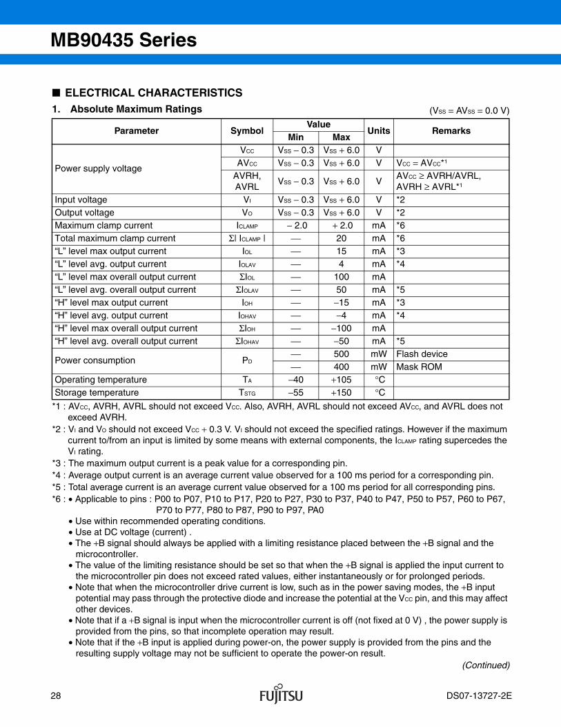
ELECTRICAL CHARACTERISTICS1. Absolute Maximum Ratings (VSS = AVSS = 0.0 V)
*1 : AVCC, AVRH, AVRL should not exceed VCC. Also, AVRH, AVRL should not exceed AVCC, and AVRL does not exceed AVRH.
*2 : VI and VO should not exceed VCC + 0.3 V. VI should not exceed the specified ratings. However if the maximum current to/from an input is limited by some means with external components, the ICLAMP rating supercedes the VI rating.
*3 : The maximum output current is a peak value for a corresponding pin.*4 : Average output current is an average current value observed for a 100 ms period for a corresponding pin.*5 : Total average current is an average current value observed for a 100 ms period for all corresponding pins.*6 : • Applicable to pins : P00 to P07, P10 to P17, P20 to P27, P30 to P37, P40 to P47, P50 to P57, P60 to P67,
P70 to P77, P80 to P87, P90 to P97, PA0• Use within recommended operating conditions.• Use at DC voltage (current) .• The +B signal should always be applied with a limiting resistance placed between the +B signal and the
microcontroller.• The value of the limiting resistance should be set so that when the +B signal is applied the input current to
the microcontroller pin does not exceed rated values, either instantaneously or for prolonged periods.• Note that when the microcontroller drive current is low, such as in the power saving modes, the +B input
potential may pass through the protective diode and increase the potential at the VCC pin, and this may affect other devices.
• Note that if a +B signal is input when the microcontroller current is off (not fixed at 0 V) , the power supply is provided from the pins, so that incomplete operation may result.
• Note that if the +B input is applied during power-on, the power supply is provided from the pins and the resulting supply voltage may not be sufficient to operate the power-on result.
(Continued)
Parameter SymbolValue
Units RemarksMin Max
Power supply voltage
VCC VSS − 0.3 VSS + 6.0 VAVCC VSS − 0.3 VSS + 6.0 V VCC = AVCC*1
AVRH, AVRL
VSS − 0.3 VSS + 6.0 VAVCC ≥ AVRH/AVRL, AVRH ≥ AVRL*1
Input voltage VI VSS − 0.3 VSS + 6.0 V *2Output voltage VO VSS − 0.3 VSS + 6.0 V *2Maximum clamp current ICLAMP − 2.0 + 2.0 mA *6Total maximum clamp current Σ| ICLAMP | ⎯ 20 mA *6“L” level max output current IOL ⎯ 15 mA *3“L” level avg. output current IOLAV ⎯ 4 mA *4“L” level max overall output current ΣIOL ⎯ 100 mA“L” level avg. overall output current ΣIOLAV ⎯ 50 mA *5“H” level max output current IOH ⎯ −15 mA *3“H” level avg. output current IOHAV ⎯ −4 mA *4“H” level max overall output current ΣIOH ⎯ −100 mA“H” level avg. overall output current ΣIOHAV ⎯ −50 mA *5
Power consumption PD⎯ 500 mW Flash device⎯ 400 mW Mask ROM
Operating temperature TA −40 +105 °CStorage temperature TSTG −55 +150 °C
28 DS07-13727-2E
MB90435 Series
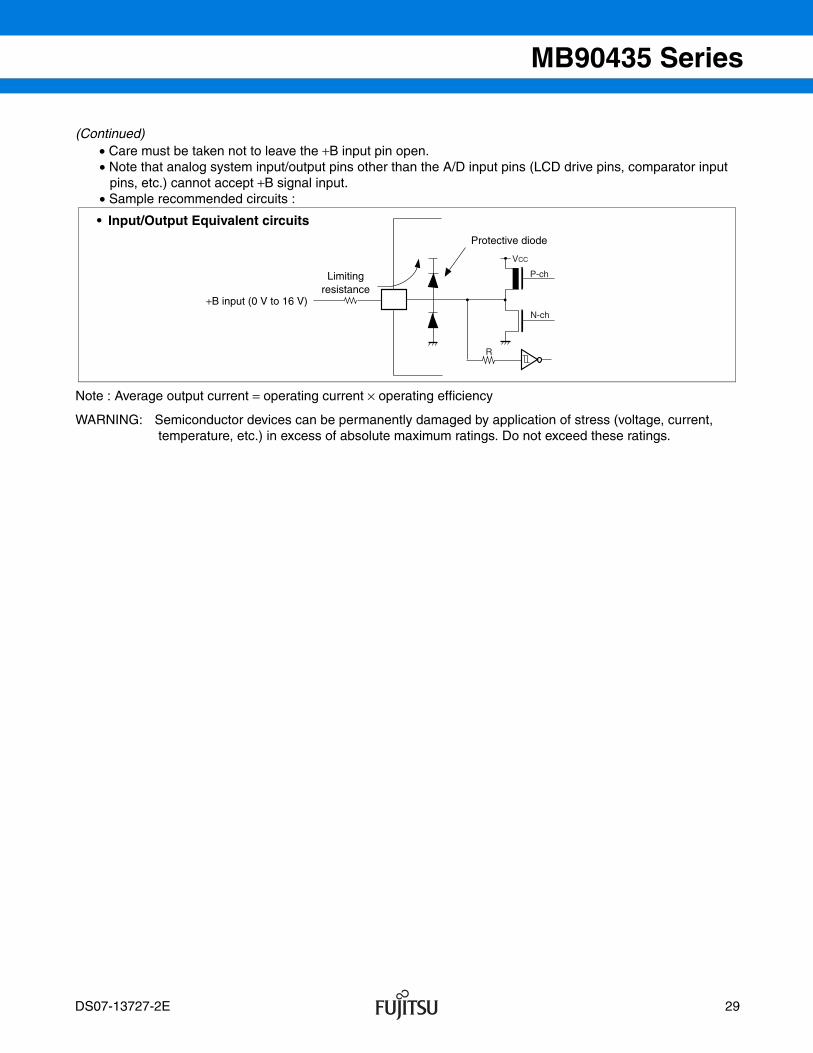
(Continued)• Care must be taken not to leave the +B input pin open.• Note that analog system input/output pins other than the A/D input pins (LCD drive pins, comparator input
pins, etc.) cannot accept +B signal input.• Sample recommended circuits :
Note : Average output current = operating current × operating efficiency
WARNING: Semiconductor devices can be permanently damaged by application of stress (voltage, current, temperature, etc.) in excess of absolute maximum ratings. Do not exceed these ratings.
P-ch
N-ch
VCC
R
• Input/Output Equivalent circuits
+B input (0 V to 16 V)
Limitingresistance
Protective diode
DS07-13727-2E 29
MB90435 Series
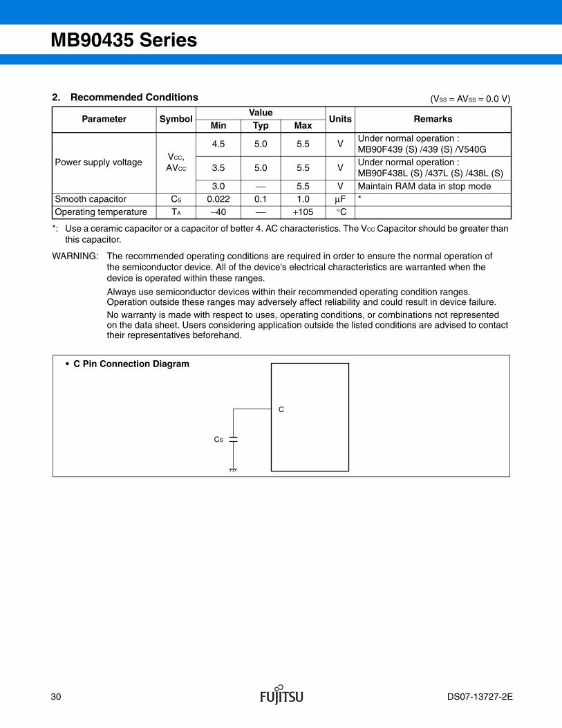
2. Recommended Conditions (VSS = AVSS = 0.0 V)
*: Use a ceramic capacitor or a capacitor of better 4. AC characteristics. The VCC Capacitor should be greater than this capacitor.
WARNING: The recommended operating conditions are required in order to ensure the normal operation of the semiconductor device. All of the device's electrical characteristics are warranted when the device is operated within these ranges.
Always use semiconductor devices within their recommended operating condition ranges. Operation outside these ranges may adversely affect reliability and could result in device failure.No warranty is made with respect to uses, operating conditions, or combinations not represented on the data sheet. Users considering application outside the listed conditions are advised to contact their representatives beforehand.
Parameter SymbolValue
Units RemarksMin Typ Max
Power supply voltageVCC, AVCC
4.5 5.0 5.5 VUnder normal operation : MB90F439 (S) /439 (S) /V540G
3.5 5.0 5.5 VUnder normal operation : MB90F438L (S) /437L (S) /438L (S)
3.0 ⎯ 5.5 V Maintain RAM data in stop modeSmooth capacitor CS 0.022 0.1 1.0 µF *Operating temperature TA −40 ⎯ +105 °C
C
CS
• C Pin Connection Diagram
30 DS07-13727-2E
MB90435 Series
3. DC Characteristics (MB90F438L (S) /437L (S) /438L (S) : VCC = 3.5 V to 5.5 V, VSS = AVSS = 0.0 V, TA = −40 °C to +105 °C)
(MB90F439 (S) /439 (S) /V540G : VCC = 5.0 V ± 10%, VSS = AVSS = 0.0 V, TA = −40 °C to +105 °C)
(Continued)
ParameterSym-bol Pin name Condition
ValueUnits Remarks
Min Typ Max
Input H voltage
VIHS
CMOS hysteresis input pin
⎯ 0.8 VCC ⎯ VCC + 0.3 V
VIHTTL input pin
⎯ 2.0 ⎯ ⎯ V
VIHMMD input pin
⎯ VCC − 0.3 ⎯ VCC + 0.3 V
Input L voltage
VILS
CMOS hysteresis input pin
⎯ VCC − 0.3 ⎯ 0.2 VCC V
VILTTL input pin
⎯ ⎯ ⎯ 0.8 V
VILMMD input pin
⎯ VSS − 0.3 ⎯ VCC + 0.3 V
Output H voltage
VOHAll output pins
VCC = 4.5 V, IOH = −4.0 mA
VCC − 0.5 ⎯ ⎯ V
Output L voltage
VOLAll output pins
VCC = 4.5 V, IOL = 4.0 mA
⎯ ⎯ 0.4 V
Input leak current
IIL ⎯ VCC = 5.5 V, VSS < VI < VCC
−5 ⎯ 5 µA
Pull-up resistance
RUP
P00 to P07,P10 to P17,P20 to P27,P30 to P37,RST
⎯ 25 50 100 kΩ
Pull-downresistance
RDO
WNMD2 ⎯ 25 50 100 kΩ
DS07-13727-2E 31
MB90435 Series
(Continued) (MB90F438L (S) /437L (S) /438L (S) : VCC = 3.5 V to 5.5 V, VSS = AVSS = 0.0 V, TA = −40 °C to +105 °C)
(MB90F439 (S) /439 (S) /V540G : VCC = 5.0 V ± 10%, VSS = AVSS = 0.0 V, TA = −40 °C to +105 °C)
* : The power supply current testing conditions are when using the external clock.
ParameterSym-bol Pin name Condition
ValueUnits Remarks
Min Typ Max
Power supply current*
ICC
VCC
Internal frequency : 16 MHz, At normal operating
⎯ 40 55 mA
Internal frequency : 16 MHz, At Flash programming/erasing
⎯ 50 70 mA Flash device
ICCSInternal frequency : 16 MHz, At sleep mode
⎯ 12 20 mA
ICTS
VCC = 5.0 V ± 1%, Internal frequency : 2 MHz, At pseudo timer mode
⎯ 300 600 µA⎯ 600 1100 µA MB90F348L (S)
⎯ 200 400 µAMB90437L (S) /438L (S)
ICCLInternal frequency : 8 kHz, At sub operation, TA = 25 °C
⎯ 400 750 µA MB90F438L (S) ⎯ 50 100 µA Mask ROM⎯ 150 300 µA Flash device
ICCLSInternal frequency : 8 kHz, At sub sleep, TA = 25 °C ⎯ 15 40 µA
ICCTInternal frequency : 8 kHz, At timer mode, TA = 25 °C ⎯ 7 25 µA
ICCH1 At stop, TA = 25 °C ⎯ 5 20 µA
ICCH2At hardware standby mode, TA = 25 °C ⎯ 50 100 µA
Inputcapacity
CIN
Other than AVCC, AVSS, AVRH, AVRL, C, VCC, VSS
⎯ ⎯ 5 15 pF
32 DS07-13727-2E
MB90435 Series
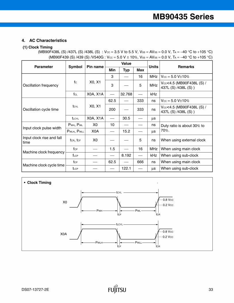
4. AC Characteristics
(1) Clock Timing (MB90F438L (S) /437L (S) /438L (S) : VCC = 3.5 V to 5.5 V, VSS = AVSS = 0.0 V, TA = −40 °C to +105 °C)
(MB90F439 (S) /439 (S) /V540G : VCC = 5.0 V ± 10%, VSS = AVSS = 0.0 V, TA = −40 °C to +105 °C)
Parameter Symbol Pin nameValue
Units RemarksMin Typ Max
Oscillation frequencyfC X0, X1
3 ⎯ 16 MHz VCC = 5.0 V±10%
3 ⎯ 5 MHzVCC<4.5 (MB90F438L (S) /437L (S) /438L (S) )
fCL X0A, X1A ⎯ 32.768 ⎯ kHz
Oscillation cycle timetCYL X0, X1
62.5 ⎯ 333 ns VCC = 5.0 V±10%
200 ⎯ 333 nsVCC<4.5 (MB90F438L (S) /437L (S) /438L (S) )
tLCYL X0A, X1A ⎯ 30.5 ⎯ µs
Input clock pulse widthPWH, PWL X0 10 ⎯ ⎯ ns Duty ratio is about 30% to
70%.PWLH, PWLL X0A ⎯ 15.2 ⎯ µs
Input clock rise and fall time
tCR, tCF X0 ⎯ ⎯ 5 ns When using external clock
Machine clock frequencyfCP ⎯ 1.5 ⎯ 16 MHz When using main clock
fLCP ⎯ ⎯ 8.192 ⎯ kHz When using sub-clock
Machine clock cycle timetCP ⎯ 62.5 ⎯ 666 ns When using main clock
tLCP ⎯ ⎯ 122.1 ⎯ µs When using sub-clock
X0
tCYL
tCF tCR
0.8 VCC
0.2 VCC
PWH PWL
X0A
tLCYL
tCF tCR
0.8 VCC
0.2 VCC
PWLH PWLL
• Clock Timing
DS07-13727-2E 33
MB90435 Series
5.5
3.5
1.5 8 16
Guaranteed operation range(MB90F438L(S)/437L(S)/438L(S))
Guaranteed PLL operation range(MB90F438L(S)/437L(S)/438L(S))
4.5
Guaranteed operation range(MB90F439(S)/439(S)/V540G)
Guaranteed PLL operation range( MB90F439(S)/439(S)/V540G)
Power supply voltageVCC (V)
Machine clock fCP (MHz)
• Guaranteed PLL operation range
16
12
89
4
3 4 8 16
×4 ×3 ×2 ×1
PLL off
• External clock frequency and Machine clock frequency
Machine clockfCP (MHz)
External clock fC (MHz)
34 DS07-13727-2E
MB90435 Series
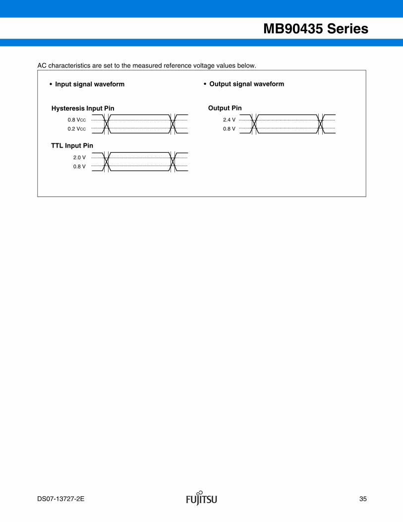
AC characteristics are set to the measured reference voltage values below.
0.8 VCC
0.2 VCC
2.4 V
0.8 V
2.0 V
0.8 V
• Input signal waveform • Output signal waveform
Hysteresis Input Pin
TTL Input Pin
Output Pin
DS07-13727-2E 35
MB90435 Series
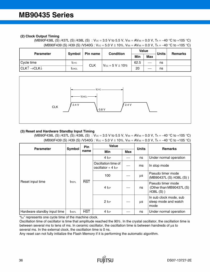
(2) Clock Output Timing (MB90F438L (S) /437L (S) /438L (S) : VCC = 3.5 V to 5.5 V, VSS = AVSS = 0.0 V, TA = −40 °C to +105 °C)
(MB90F439 (S) /439 (S) /V540G : VCC = 5.0 V ± 10%, VSS = AVSS = 0.0 V, TA = −40 °C to +105 °C)
(3) Reset and Hardware Standby Input Timing (MB90F438L (S) /437L (S) /438L (S) : VCC = 3.5 V to 5.5 V, VSS = AVSS = 0.0 V, TA = −40 °C to +105 °C)
(MB90F439 (S) /439 (S) /V540G : VCC = 5.0 V ± 10%, VSS = AVSS = 0.0 V, TA = −40 °C to +105 °C)
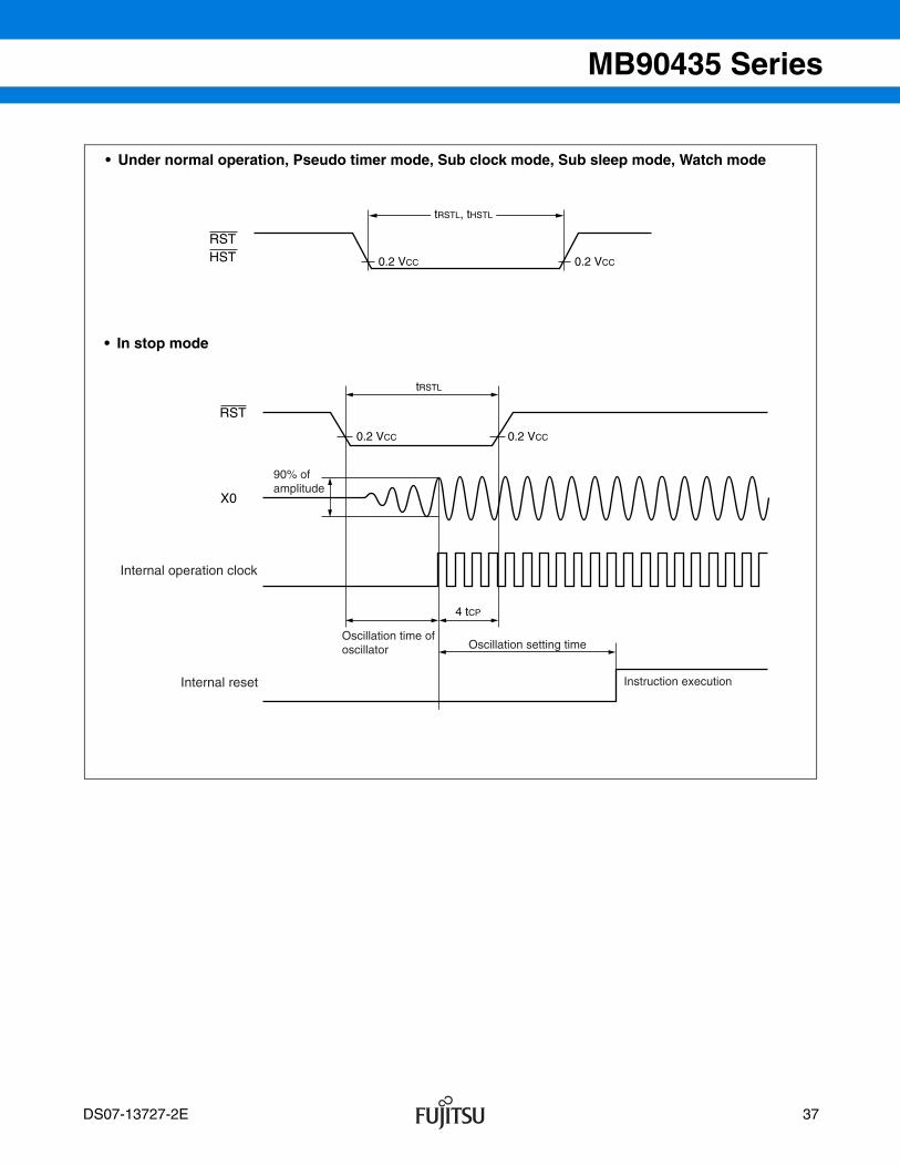
“tcp” represents one cycle time of the machine clock.Oscillation time of oscillator is time that amplitude reached the 90%. In the crystal oscillator, the oscillation time is between several ms to tens of ms. In ceramic oscillator, the oscillation time is between handreds of µs to several ms. In the external clock, the oscillation time is 0 ns.Any reset can not fully initialize the Flash Memory if it is performing the automatic algorithm.
Parameter Symbol Pin name ConditionValue
Units RemarksMin Max
Cycle time tCYCCLK VCC = 5 V ± 10%
62.5 ⎯ ns
CLK↑ →CLK↓ tCHCL 20 ⎯ ns
Parameter Symbol Pin name
ValueUnits Remarks
Min Max
Reset input time tRSTL RST
4 tCP ⎯ ns Under normal operation
Oscillation time of oscillator + 4 tCP
⎯ ms In stop mode
100 ⎯ µsPseudo timer mode (MB90437L (S) /438L (S) )
4 tCP ⎯ nsPseudo timer mode (Other than MB90437L (S) /438L (S) )
2 tCP ⎯ µsIn sub clock mode, sub sleep mode and watch mode
Hardware standby input time tHSTL HST 4 tCP ⎯ ns Under normal operation
CLK
tCYC
2.4 V 2.4 V
0.8 V
tCHCL
36 DS07-13727-2E
MB90435 Series
RSTHST 0.2 VCC
tRSTL, tHSTL
0.2 VCC
tRSTL
0.2 VCC 0.2 VCC
4 tCP
RST
X0
Internal operation clock
Internal reset
90% ofamplitude
Oscillation time ofoscillator Oscillation setting time
Instruction execution
• Under normal operation, Pseudo timer mode, Sub clock mode, Sub sleep mode, Watch mode
• In stop mode
DS07-13727-2E 37
MB90435 Series
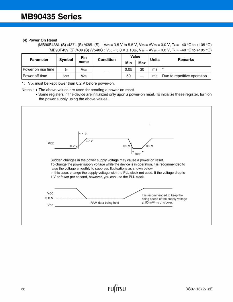
(4) Power On Reset (MB90F438L (S) /437L (S) /438L (S) : VCC = 3.5 V to 5.5 V, VSS = AVSS = 0.0 V, TA = −40 °C to +105 °C)
(MB90F439 (S) /439 (S) /V540G : VCC = 5.0 V ± 10%, VSS = AVSS = 0.0 V, TA = −40 °C to +105 °C)
* : VCC must be kept lower than 0.2 V before power-on.
Notes : • The above values are used for creating a power-on reset.• Some registers in the device are initialized only upon a power-on reset. To initialize these register, turn on the power supply using the above values.
Parameter Symbol Pin name Condition
ValueUnits Remarks
Min Max
Power on rise time tR VCC⎯
0.05 30 ms *
Power off time tOFF VCC 50 ⎯ ms Due to repetitive operation
VCC
VCC
VSS
3.0 V
tR
tOFF
2.7 V
0.2 V 0.2 V0.2 V
RAM data being held
It is recommended to keep therising speed of the supply voltageat 50 mV/ms or slower.
Sudden changes in the power supply voltage may cause a power-on reset.To change the power supply voltage while the device is in operation, it is recommended to raise the voltage smoothly to suppress fluctuations as shown below.In this case, change the supply voltage with the PLL clock not used. If the voltage drop is 1 V or fewer per second, however, you can use the PLL clock.
38 DS07-13727-2E
MB90435 Series
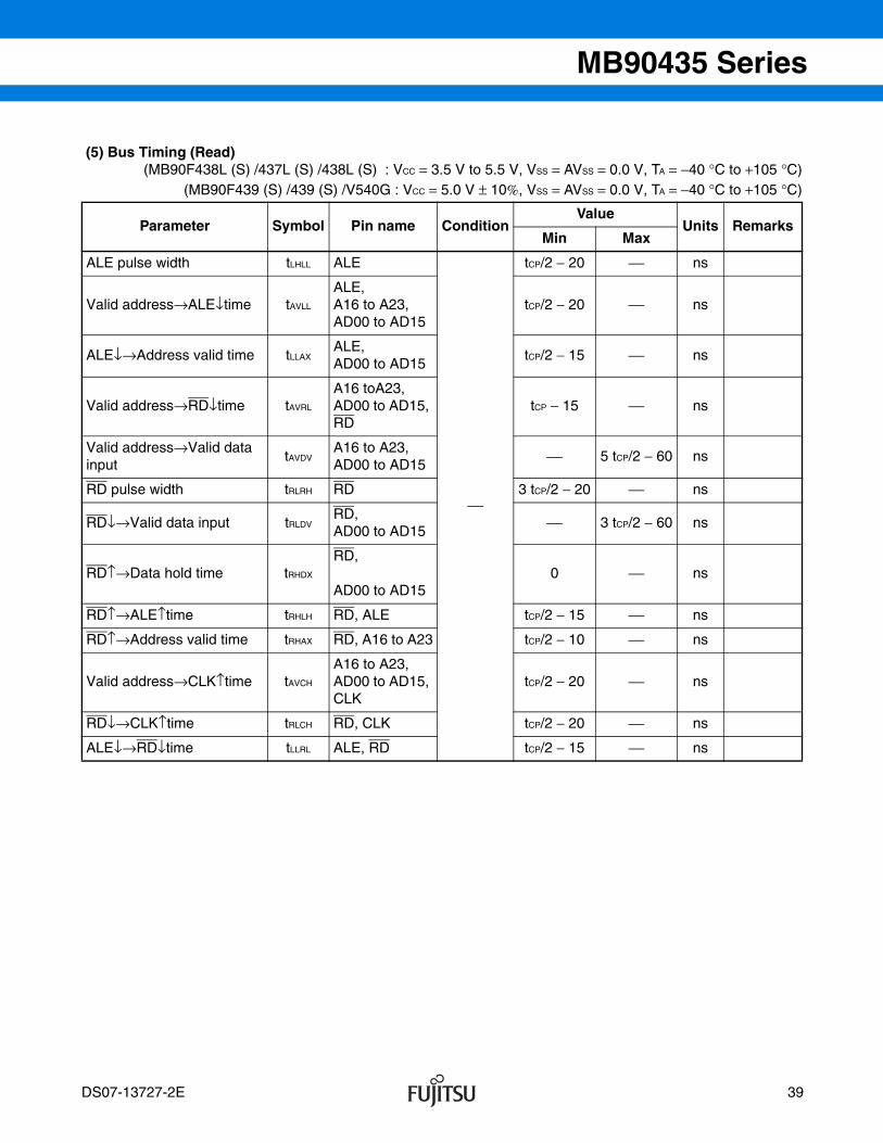
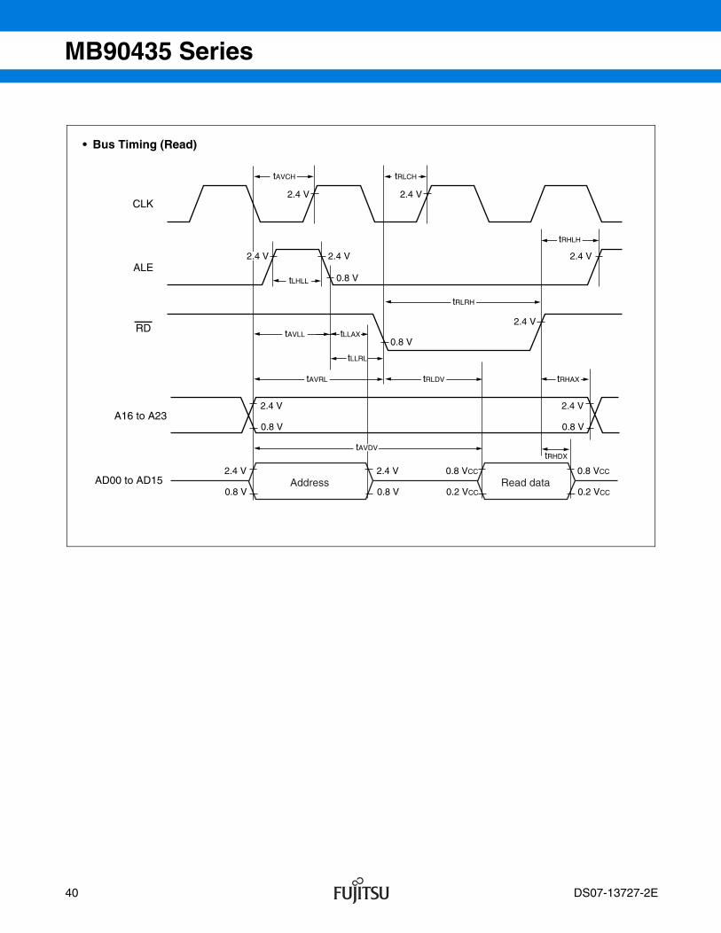
(5) Bus Timing (Read) (MB90F438L (S) /437L (S) /438L (S) : VCC = 3.5 V to 5.5 V, VSS = AVSS = 0.0 V, TA = −40 °C to +105 °C)
(MB90F439 (S) /439 (S) /V540G : VCC = 5.0 V ± 10%, VSS = AVSS = 0.0 V, TA = −40 °C to +105 °C)
Parameter Symbol Pin name ConditionValue
Units RemarksMin Max
ALE pulse width tLHLL ALE
⎯
tCP/2 − 20 ⎯ ns
Valid address→ALE↓time tAVLL
ALE, A16 to A23, AD00 to AD15
tCP/2 − 20 ⎯ ns
ALE↓→Address valid time tLLAXALE, AD00 to AD15
tCP/2 − 15 ⎯ ns
Valid address→RD↓time tAVRL
A16 toA23, AD00 to AD15, RD
tCP − 15 ⎯ ns
Valid address→Valid datainput
tAVDVA16 to A23, AD00 to AD15
⎯ 5 tCP/2 − 60 ns
RD pulse width tRLRH RD 3 tCP/2 − 20 ⎯ ns
RD↓→Valid data input tRLDVRD, AD00 to AD15
⎯ 3 tCP/2 − 60 ns
RD↑→Data hold time tRHDX
RD,
AD00 to AD150 ⎯ ns
RD↑→ALE↑time tRHLH RD, ALE tCP/2 − 15 ⎯ ns
RD↑→Address valid time tRHAX RD, A16 to A23 tCP/2 − 10 ⎯ ns
Valid address→CLK↑time tAVCH
A16 to A23, AD00 to AD15, CLK
tCP/2 − 20 ⎯ ns
RD↓→CLK↑time tRLCH RD, CLK tCP/2 − 20 ⎯ ns
ALE↓→RD↓time tLLRL ALE, RD tCP/2 − 15 ⎯ ns
DS07-13727-2E 39
asatani
ノート
asatani : Marked
asatani
ノート
asatani : Marked
MB90435 Series
0.8 V
0.8 V
2.4 V2.4 V
2.4 V
2.4 V
0.8 V
2.4 V
2.4 V
0.8 V
2.4 V
0.8 V
2.4 V
0.8 V
2.4 V
0.2 VCC
0.8 VCC
0.2 VCC
0.8 VCC
CLK
ALE
RD
A16 to A23
AD00 to AD15
2.4 V
tAVCH
tLHLL
tRHLH
tAVLL
tAVRL tRLDV
tRLRH
tRHAX
tRHDX
tLLAX
tLLRL
tRLCH
tAVDV
Address Read data
• Bus Timing (Read)
40 DS07-13727-2E
MB90435 Series
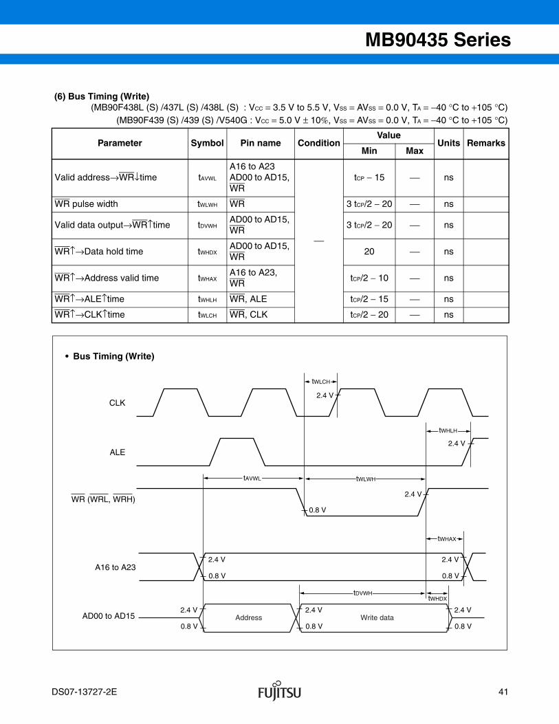
(6) Bus Timing (Write) (MB90F438L (S) /437L (S) /438L (S) : VCC = 3.5 V to 5.5 V, VSS = AVSS = 0.0 V, TA = −40 °C to +105 °C)
(MB90F439 (S) /439 (S) /V540G : VCC = 5.0 V ± 10%, VSS = AVSS = 0.0 V, TA = −40 °C to +105 °C)
Parameter Symbol Pin name ConditionValue
Units RemarksMin Max
Valid address→WR↓time tAVWL
A16 to A23 AD00 to AD15, WR
⎯
tCP − 15 ⎯ ns
WR pulse width tWLWH WR 3 tCP/2 − 20 ⎯ ns
Valid data output→WR↑time tDVWHAD00 to AD15, WR
3 tCP/2 − 20 ⎯ ns
WR↑→Data hold time tWHDXAD00 to AD15, WR
20 ⎯ ns
WR↑→Address valid time tWHAXA16 to A23, WR
tCP/2 − 10 ⎯ ns
WR↑→ALE↑time tWHLH WR, ALE tCP/2 − 15 ⎯ ns
WR↑→CLK↑time tWLCH WR, CLK tCP/2 − 20 ⎯ ns
0.8 V
0.8 V
2.4 V
2.4 V
2.4 V
2.4 V
0.8 V
2.4 V
0.8 V
2.4 V
0.8 V
2.4 V
0.8 V
2.4 V
CLK
ALE
WR (WRL, WRH)
A16 to A23
AD00 to AD15
tWHLH
tAVWL tWLWH
tWHAX
tWHDX
tWLCH
tDVWH
Address Write data
• Bus Timing (Write)
DS07-13727-2E 41
MB90435 Series
(7) Ready Input Timing (MB90F438L (S) /437L (S) /438L (S) : VCC = 3.5 V to 5.5 V, VSS = AVSS = 0.0 V, TA = −40 °C to +105 °C)
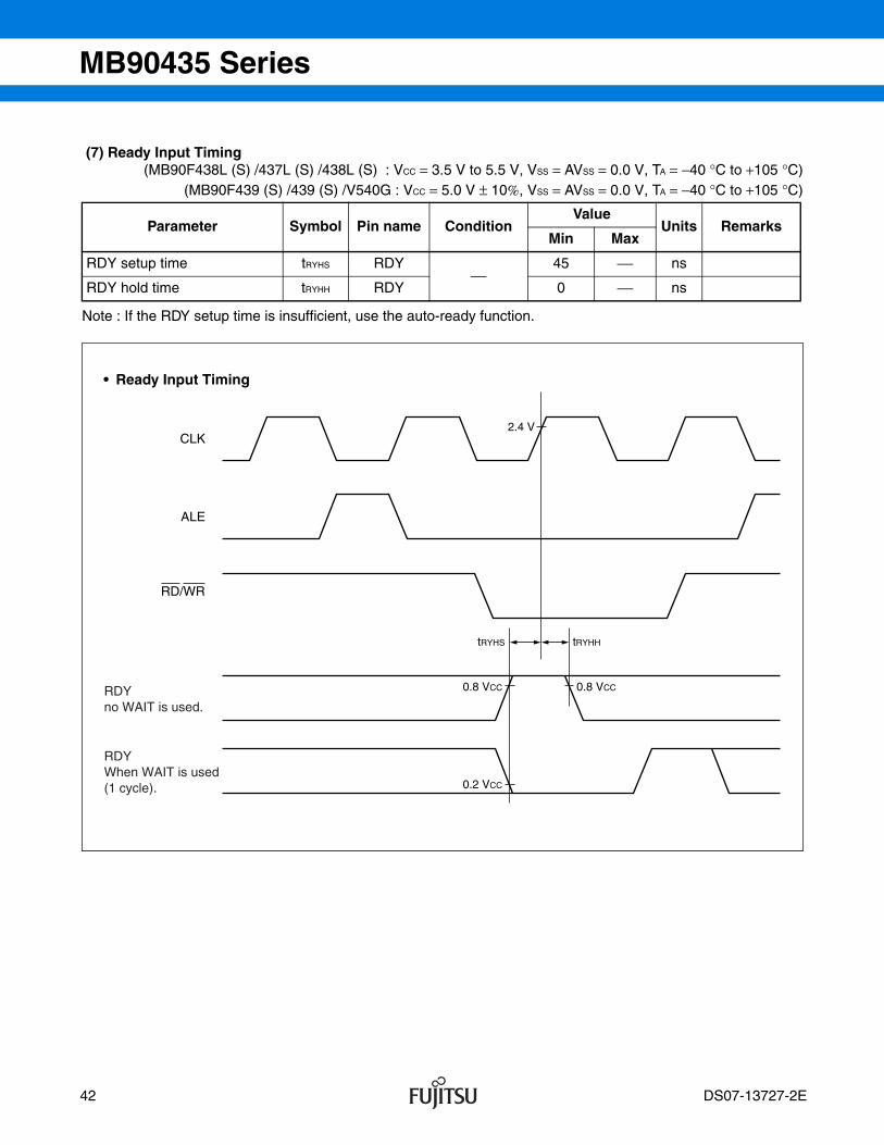
(MB90F439 (S) /439 (S) /V540G : VCC = 5.0 V ± 10%, VSS = AVSS = 0.0 V, TA = −40 °C to +105 °C)
Note : If the RDY setup time is insufficient, use the auto-ready function.
Parameter Symbol Pin name ConditionValue
Units RemarksMin Max
RDY setup time tRYHS RDY⎯
45 ⎯ ns
RDY hold time tRYHH RDY 0 ⎯ ns
tRYHS tRYHH
2.4 V
0.8 VCC
0.2 VCC
0.8 VCC
CLK
ALE
RD/WR
RDYno WAIT is used.
RDYWhen WAIT is used(1 cycle).
• Ready Input Timing
42 DS07-13727-2E
MB90435 Series
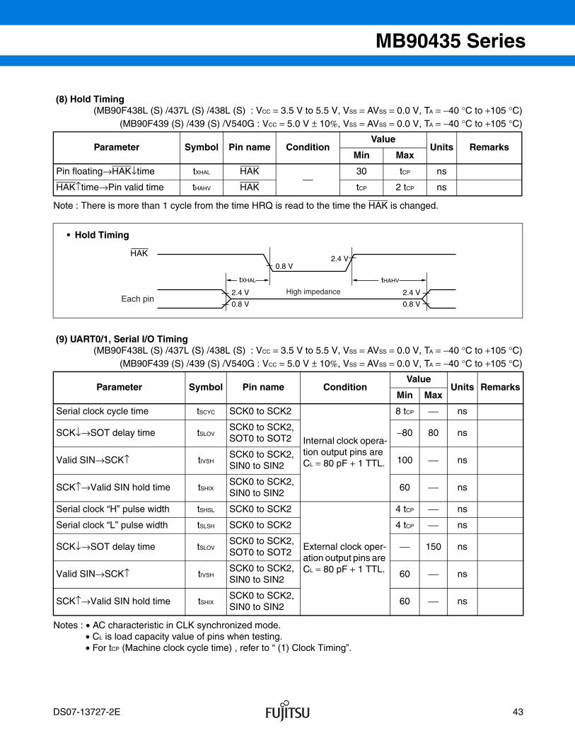
(8) Hold Timing (MB90F438L (S) /437L (S) /438L (S) : VCC = 3.5 V to 5.5 V, VSS = AVSS = 0.0 V, TA = −40 °C to +105 °C)
(MB90F439 (S) /439 (S) /V540G : VCC = 5.0 V ± 10%, VSS = AVSS = 0.0 V, TA = −40 °C to +105 °C)
Note : There is more than 1 cycle from the time HRQ is read to the time the HAK is changed.
(9) UART0/1, Serial I/O Timing (MB90F438L (S) /437L (S) /438L (S) : VCC = 3.5 V to 5.5 V, VSS = AVSS = 0.0 V, TA = −40 °C to +105 °C)
(MB90F439 (S) /439 (S) /V540G : VCC = 5.0 V ± 10%, VSS = AVSS = 0.0 V, TA = −40 °C to +105 °C)
Notes : • AC characteristic in CLK synchronized mode.• CL is load capacity value of pins when testing.• For tCP (Machine clock cycle time) , refer to “ (1) Clock Timing”.
Parameter Symbol Pin name ConditionValue
Units RemarksMin Max
Pin floating→HAK↓time tXHAL HAK⎯
30 tCP ns
HAK↑time→Pin valid time tHAHV HAK tCP 2 tCP ns
Parameter Symbol Pin name ConditionValue
Units RemarksMin Max
Serial clock cycle time tSCYC SCK0 to SCK2
Internal clock opera-tion output pins are CL = 80 pF + 1 TTL.
8 tCP ⎯ ns
SCK↓→SOT delay time tSLOVSCK0 to SCK2, SOT0 to SOT2
−80 80 ns
Valid SIN→SCK↑ tIVSHSCK0 to SCK2, SIN0 to SIN2
100 ⎯ ns
SCK↑→Valid SIN hold time tSHIXSCK0 to SCK2, SIN0 to SIN2
60 ⎯ ns
Serial clock “H” pulse width tSHSL SCK0 to SCK2
External clock oper-ation output pins are CL = 80 pF + 1 TTL.
4 tCP ⎯ ns
Serial clock “L” pulse width tSLSH SCK0 to SCK2 4 tCP ⎯ ns
SCK↓→SOT delay time tSLOVSCK0 to SCK2, SOT0 to SOT2
⎯ 150 ns
Valid SIN→SCK↑ tIVSHSCK0 to SCK2, SIN0 to SIN2
60 ⎯ ns
SCK↑→Valid SIN hold time tSHIXSCK0 to SCK2, SIN0 to SIN2
60 ⎯ ns
HAK
tXHAL tHAHV
2.4 V
0.8 V
2.4 V
2.4 V
0.8 V
0.8 V
Each pinHigh impedance
• Hold Timing
DS07-13727-2E 43
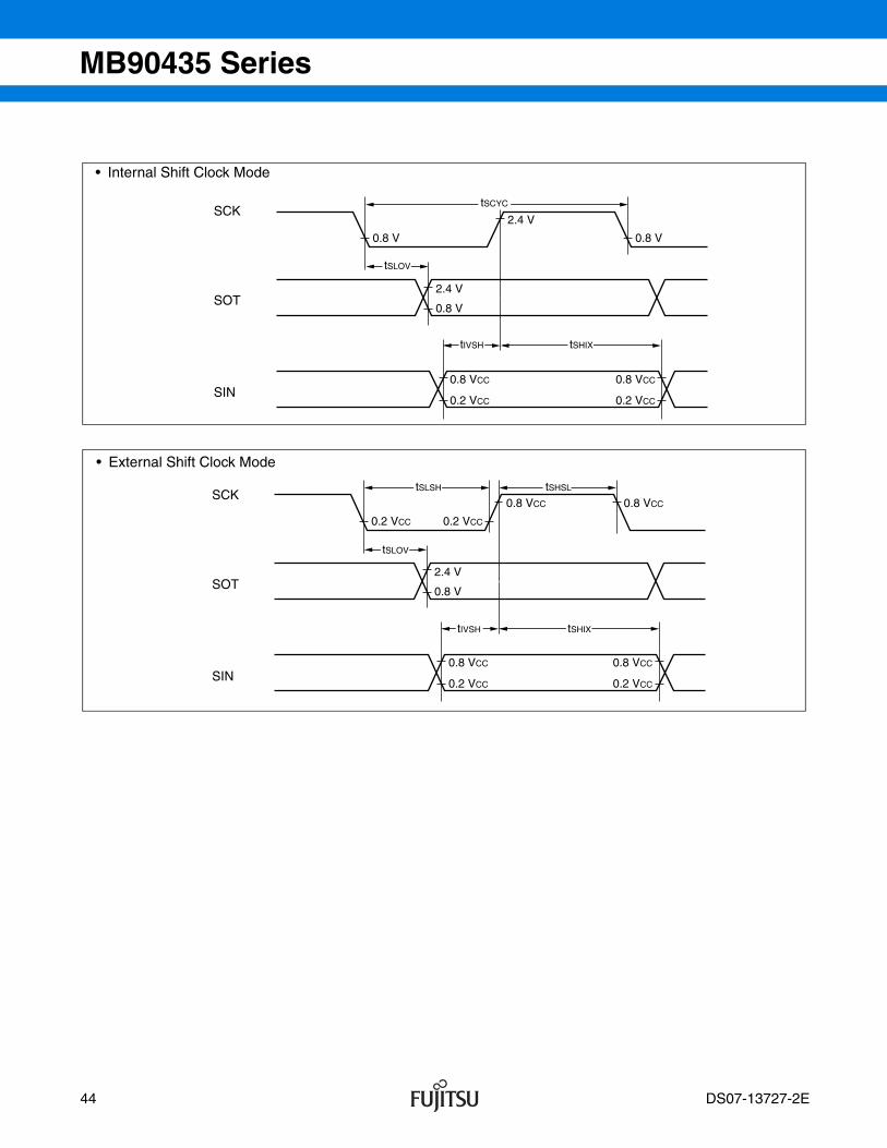
MB90435 Series
SCK
SOT
SIN
tSCYC
tSLOV
tIVSH tSHIX
0.8 V 0.8 V
2.4 V
2.4 V
0.8 V
0.8 VCC
0.2 VCC
0.8 VCC
0.2 VCC
• Internal Shift Clock Mode
SCK
SOT
SIN
tSLSH tSHSL
tSLOV
tIVSH tSHIX
0.2 VCC 0.2 VCC
0.8 VCC 0.8 VCC
2.4 V
0.8 V
0.8 VCC
0.2 VCC
0.8 VCC
0.2 VCC
• External Shift Clock Mode
44 DS07-13727-2E
MB90435 Series
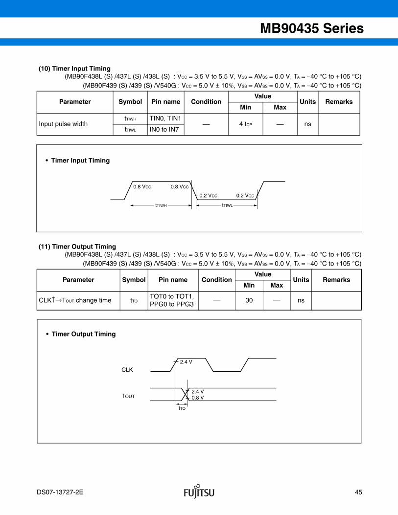
(10) Timer Input Timing (MB90F438L (S) /437L (S) /438L (S) : VCC = 3.5 V to 5.5 V, VSS = AVSS = 0.0 V, TA = −40 °C to +105 °C)
(MB90F439 (S) /439 (S) /V540G : VCC = 5.0 V ± 10%, VSS = AVSS = 0.0 V, TA = −40 °C to +105 °C)
(11) Timer Output Timing (MB90F438L (S) /437L (S) /438L (S) : VCC = 3.5 V to 5.5 V, VSS = AVSS = 0.0 V, TA = −40 °C to +105 °C)
(MB90F439 (S) /439 (S) /V540G : VCC = 5.0 V ± 10%, VSS = AVSS = 0.0 V, TA = −40 °C to +105 °C)
Parameter Symbol Pin name ConditionValue
Units RemarksMin Max
Input pulse widthtTIWH TIN0, TIN1
⎯ 4 tCP ⎯ nstTIWL IN0 to IN7
Parameter Symbol Pin name ConditionValue
Units RemarksMin Max
CLK↑→TOUT change time tTOTOT0 to TOT1, PPG0 to PPG3
⎯ 30 ⎯ ns
0.8 VCC 0.8 VCC
0.2 VCC 0.2 VCC
tTIWH tTIWL
• Timer Input Timing
CLK
TOUT
2.4 V
tTO
2.4 V0.8 V
• Timer Output Timing
DS07-13727-2E 45
MB90435 Series
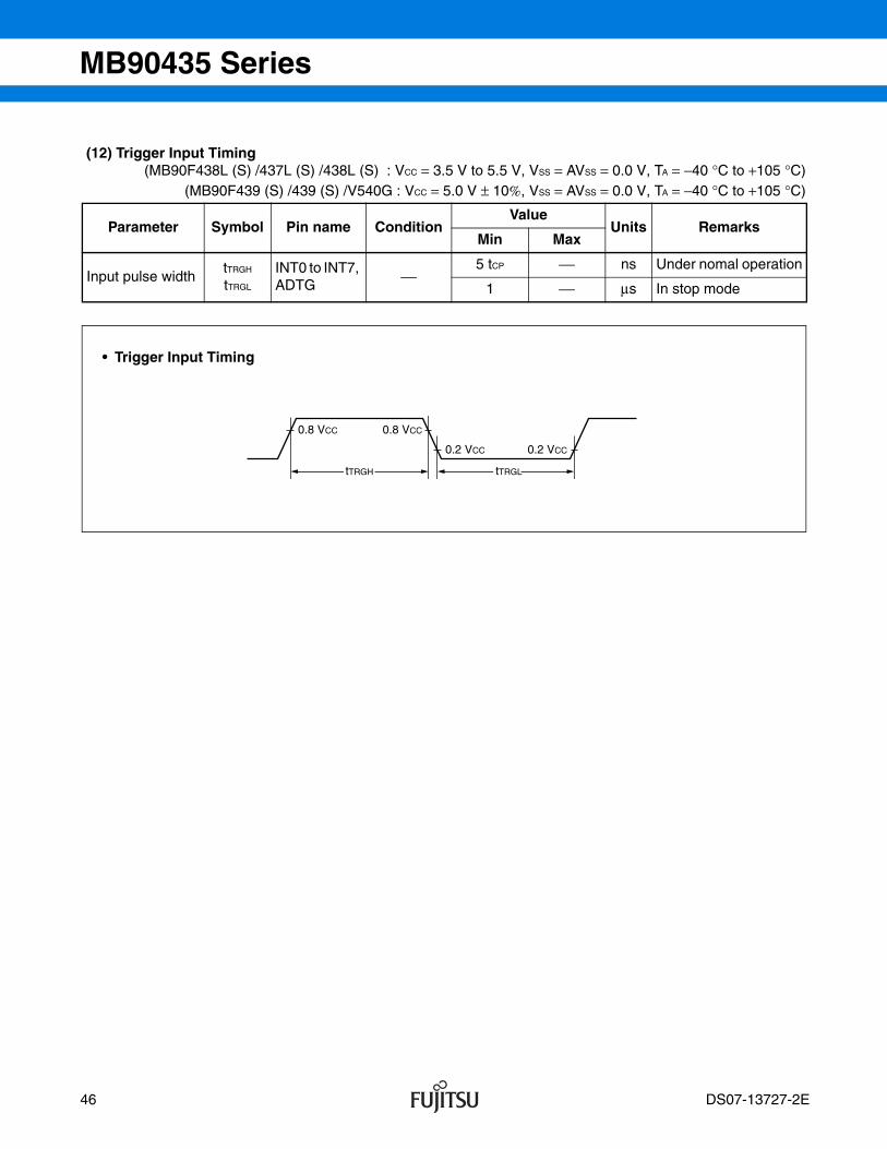
(12) Trigger Input Timing (MB90F438L (S) /437L (S) /438L (S) : VCC = 3.5 V to 5.5 V, VSS = AVSS = 0.0 V, TA = −40 °C to +105 °C)
(MB90F439 (S) /439 (S) /V540G : VCC = 5.0 V ± 10%, VSS = AVSS = 0.0 V, TA = −40 °C to +105 °C)
Parameter Symbol Pin name ConditionValue
Units RemarksMin Max
Input pulse widthtTRGH
tTRGL
INT0 to INT7, ADTG
⎯5 tCP ⎯ ns Under nomal operation
1 ⎯ µs In stop mode
0.8 VCC 0.8 VCC
0.2 VCC 0.2 VCC
tTRGH tTRGL
• Trigger Input Timing
46 DS07-13727-2E
MB90435 Series
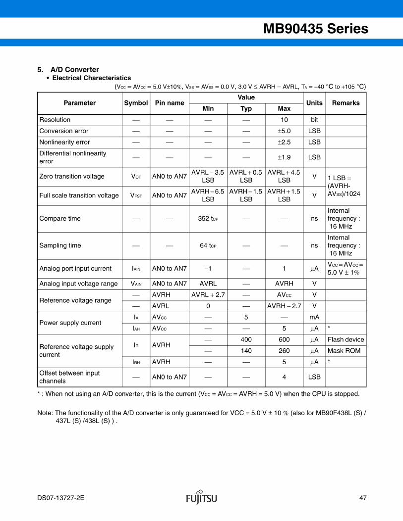
5. A/D Converter• Electrical Characteristics
(VCC = AVCC = 5.0 V±10%, VSS = AVSS = 0.0 V, 3.0 V ≤ AVRH − AVRL, TA = −40 °C to +105 °C)
* : When not using an A/D converter, this is the current (VCC = AVCC = AVRH = 5.0 V) when the CPU is stopped.
Note: The functionality of the A/D converter is only guaranteed for VCC = 5.0 V ± 10 % (also for MB90F438L (S) /437L (S) /438L (S) ) .
Parameter Symbol Pin nameValue
Units RemarksMin Typ Max
Resolution ⎯ ⎯ ⎯ ⎯ 10 bit
Conversion error ⎯ ⎯ ⎯ ⎯ ±5.0 LSB
Nonlinearity error ⎯ ⎯ ⎯ ⎯ ±2.5 LSB
Differential nonlinearityerror
⎯ ⎯ ⎯ ⎯ ±1.9 LSB
Zero transition voltage VOT AN0 to AN7AVRL − 3.5
LSBAVRL + 0.5
LSBAVRL + 4.5
LSBV 1 LSB =
(AVRH-AVSS)/1024Full scale transition voltage VFST AN0 to AN7
AVRH − 6.5 LSB
AVRH − 1.5 LSB
AVRH + 1.5 LSB
V
Compare time ⎯ ⎯ 352 tCP ⎯ ⎯ nsInternal frequency : 16 MHz
Sampling time ⎯ ⎯ 64 tCP ⎯ ⎯ nsInternal frequency : 16 MHz
Analog port input current IAIN AN0 to AN7 −1 ⎯ 1 µAVCC = AVCC = 5.0 V ± 1%
Analog input voltage range VAIN AN0 to AN7 AVRL ⎯ AVRH V
Reference voltage range⎯ AVRH AVRL + 2.7 ⎯ AVCC V
⎯ AVRL 0 ⎯ AVRH − 2.7 V
Power supply currentIA AVCC ⎯ 5 ⎯ mA
IAH AVCC ⎯ ⎯ 5 µA *
Reference voltage supply current
IR AVRH⎯ 400 600 µA Flash device
⎯ 140 260 µA Mask ROM
IRH AVRH ⎯ ⎯ 5 µA *
Offset between inputchannels
⎯ AN0 to AN7 ⎯ ⎯ 4 LSB
DS07-13727-2E 47
asatani
ノート
asatani : Marked
Changed the item of “Zero transition voltage” and “Full-scale transition voltage”.
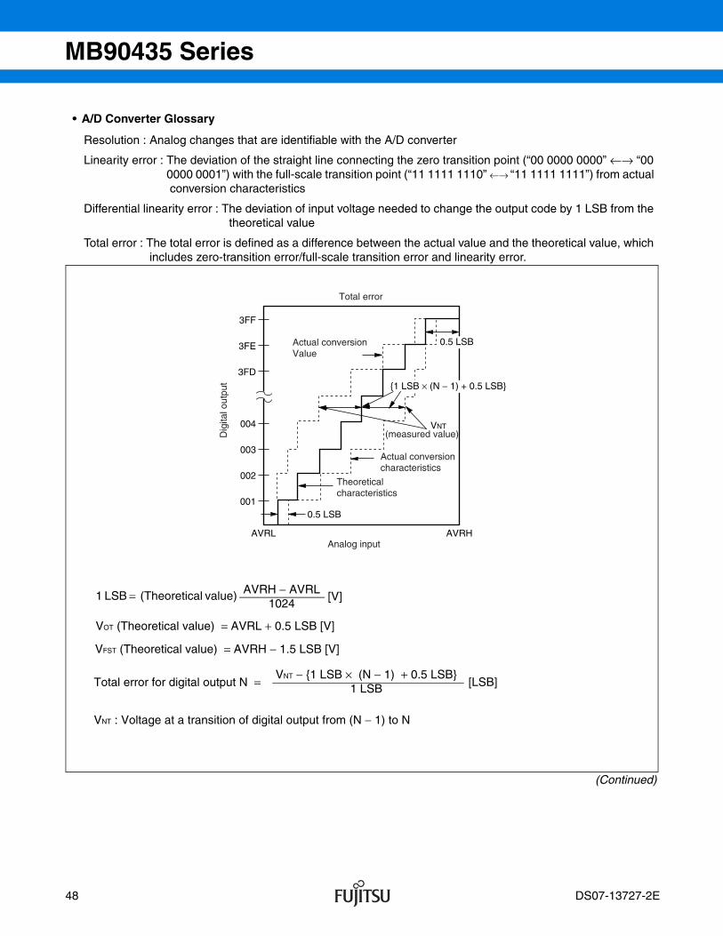
MB90435 Series
• A/D Converter Glossary
Resolution : Analog changes that are identifiable with the A/D converter
Linearity error : The deviation of the straight line connecting the zero transition point (“00 0000 0000” ←→ “00 0000 0001”) with the full-scale transition point (“11 1111 1110” ←→ “11 1111 1111”) from actual conversion characteristics
Differential linearity error : The deviation of input voltage needed to change the output code by 1 LSB from the theoretical value
Total error : The total error is defined as a difference between the actual value and the theoretical value, which includes zero-transition error/full-scale transition error and linearity error.
(Continued)
3FF
3FE
3FD
004
003
002
001
AVRL AVRH
VNT
0.5 LSB
0.5 LSB
1 LSB × (N − 1) + 0.5 LSB
Analog input
Dig
ital o
utpu
t
Total error
Actual conversionValue
Actual conversioncharacteristics
(measured value)
Theoreticalcharacteristics
[V]AVRH − AVRL
10241 LSB = (Theoretical value)
VOT (Theoretical value) = AVRL + 0.5 LSB [V]
VFST (Theoretical value) = AVRH − 1.5 LSB [V]
Total error for digital output N = [LSB]VNT − 1 LSB × (N − 1) + 0.5 LSB
1 LSB
VNT : Voltage at a transition of digital output from (N − 1) to N
48 DS07-13727-2E
MB90435 Series
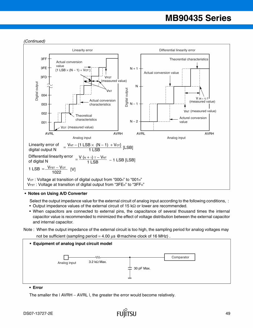
(Continued)
• Notes on Using A/D Converter
Select the output impedance value for the external circuit of analog input according to the following conditions, : • Output impedance values of the external circuit of 15 kΩ or lower are recommended.• When capacitors are connected to external pins, the capacitance of several thousand times the internal
capacitor value is recommended to minimized the effect of voltage distribution between the external capacitorand internal capacitor.
Note : When the output impedance of the external circuit is too high, the sampling period for analog voltages may
not be sufficient (sampling period = 4.00 µs @machine clock of 16 MHz) .
• Error
The smaller the | AVRH − AVRL |, the greater the error would become relatively.
3FF
3FE
3FD
004
003
002
001
AVRL AVRH AVRL AVRH
N + 1
N
N − 1
N − 2
VNT
VNT
V (N + 1) T
VOT
VFST
1 LSB × (N − 1) + VOT
Dig
ital o
utpu
t
Dig
ital o
utpu
t
Linearity error Differential linearity error
Analog input Analog input
Actual conversionvalue
(measured value)
Actual conversioncharacteristics
Theoreticalcharacteristics
(measured value)
Theorential characteristics
Actual conversion value
(measured value)
(measured value)
Acturel conversionvalue
Linearity error ofdigital output N [LSB]
VNT − 1 LSB × (N − 1) + VOT1 LSB
[V]VFST − VOT
10221 LSB
− 1 LSB [LSB]V (N + 1) T − VNT
1 LSBDifferential linearity error of digital N
VOT : Voltage at transition of digital output from “000H” to “001H”VFST : Voltage at transition of digital output from “3FEH” to “3FFH”
=
=
=
3.2 kΩ Max.
30 pF Max.
Analog input
Comparator
• Equipment of analog input circuit model
DS07-13727-2E 49
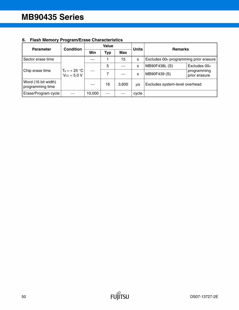
MB90435 Series
6. Flash Memory Program/Erase Characteristics
Parameter ConditionValue
Units RemarksMin Typ Max
Sector erase time
TA = + 25 °CVCC = 5.0 V
⎯ 1 15 s Excludes 00H programming prior erasure
Chip erase time ⎯5 ⎯ s MB90F438L (S) Excludes 00H
programming prior erasure7 ⎯ s MB90F439 (S)
Word (16 bit width) programming time
⎯ 16 3,600 µs Excludes system-level overhead
Erase/Program cycle ⎯ 10,000 ⎯ ⎯ cycle
50 DS07-13727-2E
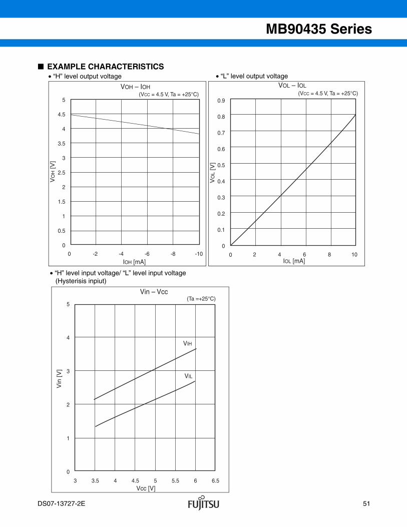
MB90435 Series
EXAMPLE CHARACTERISTICS
5
4.5
4
3.5
3
2.5
2
1.5
1
0.5
0
0 -10-8-6-4-2
IOH [mA]
VO
H [V
]
VOH – IOH
0.9
0.8
0.7
0.6
0.5
0.4
0.3
0.2
0.1
0
0 108642IOL [mA]
VO
L [V
]
VOL – IOL
(VCC = 4.5 V, Ta = +25°C) (VCC = 4.5 V, Ta = +25°C)
5
4
3
2
1
0
3 5.554.543.5Vcc [V]
Vin
[V
]
Vin – Vcc
6 6.5
VIH
VIL
(Ta =+25°C)
• “H” level output voltage
• “H” level input voltage/ “L” level input voltage (Hysterisis inpiut)
• “L” level output voltage
DS07-13727-2E 51
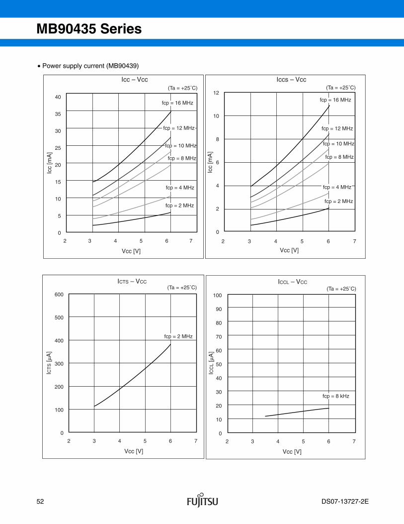
MB90435 Series
• Power supply current (MB90439)
40
35
30
25
20
15
10
5
0
2 76543
Vcc [V]
Icc
[mA
]
Icc – Vcc
fcp = 12 MHz
fcp = 16 MHz
fcp = 10 MHz
fcp = 8 MHz
fcp = 4 MHz
fcp = 2 MHz
12
10
8
6
4
2
0
2 76543
Vcc [V]
Icc
[mA
]
Iccs – Vcc
fcp = 12 MHz
fcp = 16 MHz
fcp = 10 MHz
fcp = 8 MHz
fcp = 4 MHz
fcp = 2 MHz
600
500
400
300
200
100
0
2 76543
Vcc [V]
ICT
S [µ
A]
ICTS – VCC
fcp = 2 MHz
60
50
40
30
20
10
0
2 76543
Vcc [V]
ICC
L [µ
A]
ICCL – VCC
fcp = 8 kHz
70
80
90
100
(Ta = +25˚C) (Ta = +25˚C)
(Ta = +25˚C) (Ta = +25˚C)
52 DS07-13727-2E
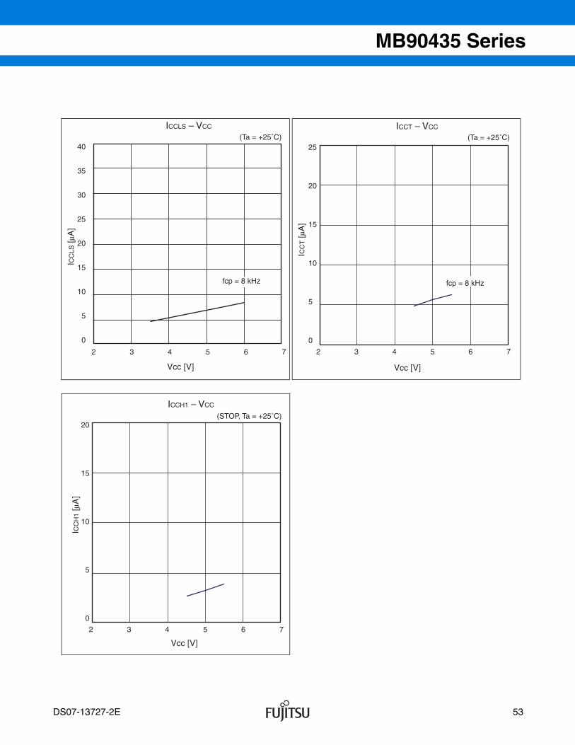
MB90435 Series
40
35
30
25
20
15
10
5
0
Vcc [V]
ICC
LS [µ
A]
ICCLS – VCC
fcp = 8 kHz
25
20
15
10
5
0
2 76543
Vcc [V]
ICC
T [µ
A]
ICCT – VCC
20
15
10
5
0
2 76543
Vcc [V]
ICC
H1
[µA
]
ICCH1 – VCC
2 76543
(STOP, Ta = +25˚C)
(Ta = +25˚C) (Ta = +25˚C)
fcp = 8 kHz
DS07-13727-2E 53
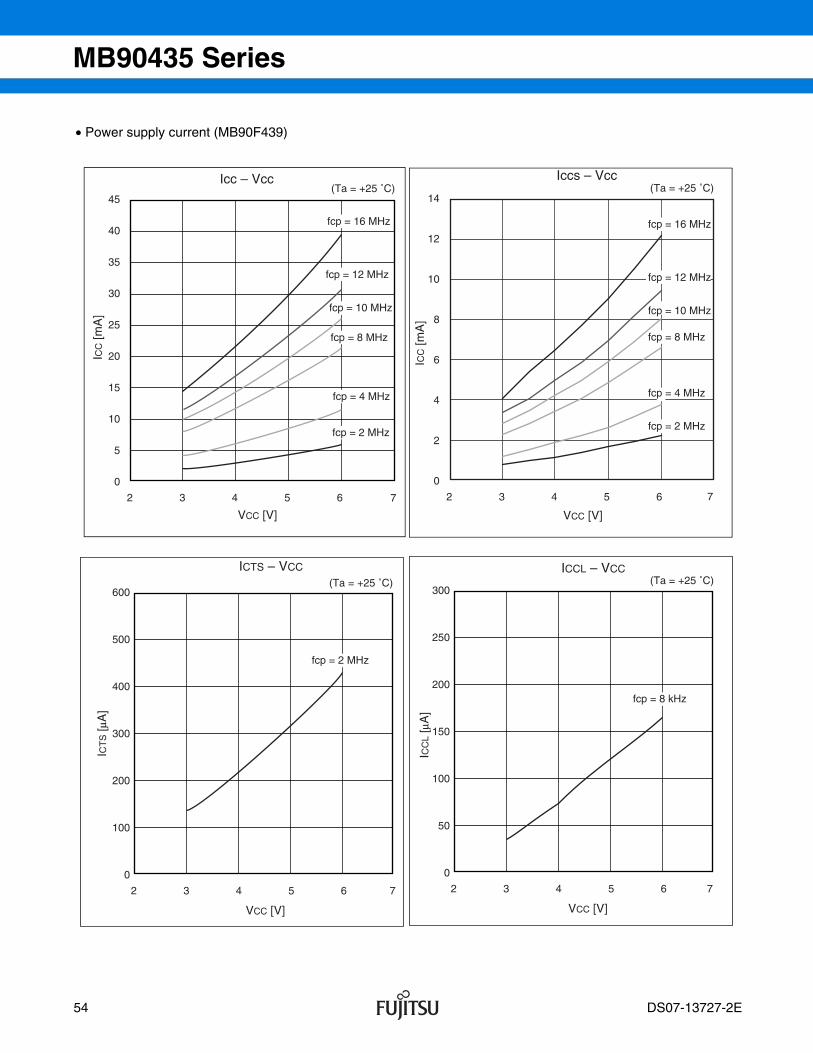
MB90435 Series
• Power supply current (MB90F439)
45
40
35
30
25
20
15
10
5
0
2 3 4 5 6
fcp = 8 MHz
fcp = 4 MHz
fcp = 2 MHz
fcp = 16 MHz
fcp = 12 MHz
fcp = 10 MHz
Icc – Vcc
ICC
[mA
]
VCC [V]
14
12
10
8
6
4
2
0
2 3 4 5 6
Iccs – Vcc
ICC
[mA
]
VCC [V]
600
500
400
300
200
100
0
2 3 4 5 6
fcp = 2 MHz
ICTS – VCC
ICT
S [µ
A]
VCC [V]
300
250
200
150
100
50
0
2 3 4 5 6
fcp = 8 kHz
ICCL – VCC
ICC
L [µ
A]
VCC [V]
7 7
7 7
(Ta = +25 ˚C) (Ta = +25 ˚C)
(Ta = +25 ˚C) (Ta = +25 ˚C)
fcp = 8 MHz
fcp = 4 MHz
fcp = 2 MHz
fcp = 16 MHz
fcp = 12 MHz
fcp = 10 MHz
54 DS07-13727-2E
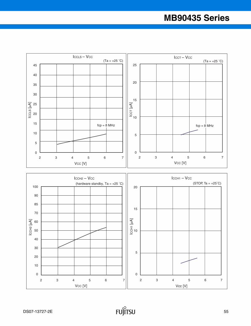
MB90435 Series
45
40
35
30
25
20
15
10
5
0
2 3 4 5 6
fcp = 8 MHz
ICCLS – VCC
ICC
LS [µ
A]
VCC [V]
7
25
20
15
10
5
0
2 3 4 5 6
ICCT – VCC
ICC
T [µ
A]
VCC [V]
7
100
90
85
70
60
50
40
30
20
0
2 3 4 5 6
ICCH2 – VCC
ICC
H2
[µA
]
VCC [V]
7
10
(hardware standby, Ta = +25 ˚C)
(Ta = +25 ˚C)(Ta = +25 ˚C)
fcp = 8 MHz
20
15
10
5
0
2 76543
Vcc [V]
ICC
H1
[µA
]
ICCH1 – VCC
(STOP, Ta = +25˚C)
DS07-13727-2E 55
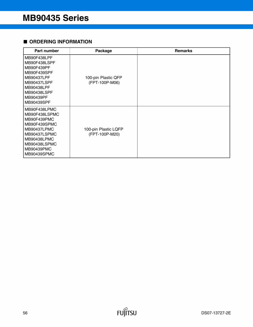
MB90435 Series
ORDERING INFORMATION
Part number Package Remarks
MB90F438LPFMB90F438LSPFMB90F439PFMB90F439SPFMB90437LPFMB90437LSPFMB90438LPFMB90438LSPFMB90439PFMB90439SPF
100-pin Plastic QFP (FPT-100P-M06)
MB90F438LPMCMB90F438LSPMCMB90F439PMCMB90F439SPMCMB90437LPMCMB90437LSPMCMB90438LPMCMB90438LSPMCMB90439PMCMB90439SPMC
100-pin Plastic LQFP (FPT-100P-M20)
56 DS07-13727-2E
Changed the part number; MB90437LPFV-> MB90437LPMC MB90437LSPFV-> MB90437LSPMC MB90438LPFV-> MB90438LPMC MB90438LSPFV -> MB90438LSPMC MB90439PFV-> MB90439PMC MB90439SPFV-> MB90439SPMC MB90F438LPFV-> MB90F438LPMC MB90F438LSPFV-> MB90F438LSPMC MB90F439PFV-> MB90F439PMC MB90F439SPFV-> MB90F439SPMC
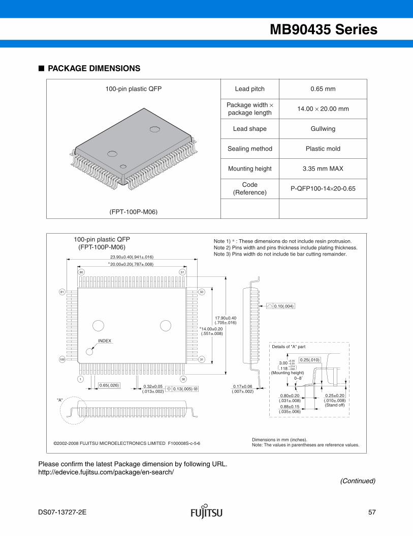
MB90435 Series
PACKAGE DIMENSIONS
Please confirm the latest Package dimension by following URL.http://edevice.fujitsu.com/package/en-search/
(Continued)
100-pin plastic QFP Lead pitch 0.65 mm
Package width ×package length
14.00 × 20.00 mm
Lead shape Gullwing
Sealing method Plastic mold
Mounting height 3.35 mm MAX
Code(Reference)
P-QFP100-14×20-0.65
100-pin plastic QFP(FPT-100P-M06)
(FPT-100P-M06)
C 2002 FUJITSU LIMITED F100008S-c-5-5
1 30
31
50
5180
81
100
20.00±0.20(.787±.008)
23.90±0.40(.941±.016)
14.00±0.20(.551±.008)
17.90±0.40(.705±.016)
INDEX
0.65(.026) 0.32±0.05(.013±.002)
M0.13(.005)
"A"
0.17±0.06(.007±.002)
0.10(.004)
Details of "A" part
(.035±.006)0.88±0.15
(.031±.008)0.80±0.20
0.25(.010)3.00
+0.35–0.20+.014–.008.118
(Mounting height)
0.25±0.20(.010±.008)(Stand off)
0~8˚
*
*
Dimensions in mm (inches).Note: The values in parentheses are reference values.©2002-2008 FUJITSU MICROELECTRONICS LIMITED F100008S-c-5-6
Note 1) * : These dimensions do not include resin protrusion.Note 2) Pins width and pins thickness include plating thickness.Note 3) Pins width do not include tie bar cutting remainder.
DS07-13727-2E 57
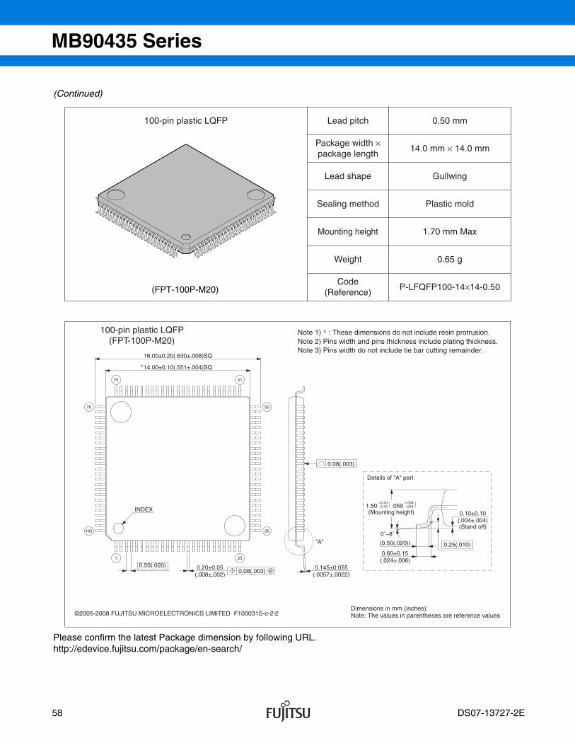
MB90435 Series
(Continued)
Please confirm the latest Package dimension by following URL.http://edevice.fujitsu.com/package/en-search/
100-pin plastic LQFP Lead pitch 0.50 mm
Package width ×package length
14.0 mm × 14.0 mm
Lead shape Gullwing
Sealing method Plastic mold
Mounting height 1.70 mm Max
Weight 0.65 g
Code(Reference)
P-LFQFP100-14×14-0.50
100-pin plastic LQFP(FPT-100P-M20)
(FPT-100P-M20)
C 2005 FUJITSU LIMITED F100031S-c-2-1
14.00±0.10(.551±.004)SQ
16.00±0.20(.630±.008)SQ
1 25
26
51
76 50
75
100
0.50(.020) 0.20±0.05(.008±.002)
M0.08(.003)0.145±0.055
(.0057±.0022)
0.08(.003)
"A"
INDEX.059 –.004
+.008–0.10+0.20
1.50(Mounting height)
0˚~8˚
(0.50(.020))
(.024±.006)0.60±0.15
0.25(.010)
0.10±0.10(.004±.004)
Details of "A" part
(Stand off)
*
Dimensions in mm (inches).Note: The values in parentheses are reference values©2005-2008 FUJITSU MICROELECTRONICS LIMITED F100031S-c-2-2
Note 1) * : These dimensions do not include resin protrusion.Note 2) Pins width and pins thickness include plating thickness.Note 3) Pins width do not include tie bar cutting remainder.
58 DS07-13727-2E
Changed the figure of package. FPT-100P-M05 -> FPT-100P-M20
MB90435 Series
MAIN CHANGES IN THIS EDITION
The vertical lines marked in the left side of the page show the changes.
Page Section Change Results
⎯ ⎯ Changed the package. (FPT-100P-M05 → FPT-100P-M20)
47 ELECTRICAL CHARACTERISTICS5. A/D Converter
Changed the item of “Zero transition voltage” and “Full-scale transition voltage”.
56
ORDERING INFORMATION Changed the part number;MB90437LPFV→ MB90437LPMC MB90437LSPFV→ MB90437LSPMC MB90438LPFV→ MB90438LPMC MB90438LSPFV → MB90438LSPMC MB90439PFV→ MB90439PMC MB90439SPFV→ MB90439SPMC MB90F438LPFV→ MB90F438LPMC MB90F438LSPFV→ MB90F438LSPMC MB90F439PFV→ MB90F439PMC MB90F439SPFV→ MB90F439SPMC
57 PACKAGE DIMENSIONS Changed the figure of package.
FPT-100P-M05 → FPT-100P-M20
DS07-13727-2E 59
MB90435 Series
FUJITSU MICROELECTRONICS LIMITEDShinjuku Dai-Ichi Seimei Bldg. 7-1, Nishishinjuku 2-chome, Shinjuku-ku,Tokyo 163-0722, Japan Tel: +81-3-5322-3347 Fax: +81-3-5322-3387http://jp.fujitsu.com/fml/en/
For further information please contact:
North and South AmericaFUJITSU MICROELECTRONICS AMERICA, INC.1250 E. Arques Avenue, M/S 333Sunnyvale, CA 94085-5401, U.S.A.Tel: +1-408-737-5600 Fax: +1-408-737-5999http://www.fma.fujitsu.com/
EuropeFUJITSU MICROELECTRONICS EUROPE GmbHPittlerstrasse 47, 63225 Langen,GermanyTel: +49-6103-690-0 Fax: +49-6103-690-122http://emea.fujitsu.com/microelectronics/
KoreaFUJITSU MICROELECTRONICS KOREA LTD.206 KOSMO TOWER, 1002 Daechi-Dong,Kangnam-Gu,Seoul 135-280KoreaTel: +82-2-3484-7100 Fax: +82-2-3484-7111http://www.fmk.fujitsu.com/
Asia PacificFUJITSU MICROELECTRONICS ASIA PTE LTD.151 Lorong Chuan, #05-08 New Tech Park,Singapore 556741Tel: +65-6281-0770 Fax: +65-6281-0220http://www.fujitsu.com/sg/services/micro/semiconductor/
FUJITSU MICROELECTRONICS SHANGHAI CO., LTD.Rm.3102, Bund Center, No.222 Yan An Road(E),Shanghai 200002, ChinaTel: +86-21-6335-1560 Fax: +86-21-6335-1605http://cn.fujitsu.com/fmc/
FUJITSU MICROELECTRONICS PACIFIC ASIA LTD.10/F., World Commerce Centre, 11 Canton RoadTsimshatsui, KowloonHong KongTel: +852-2377-0226 Fax: +852-2376-3269http://cn.fujitsu.com/fmc/tw
All Rights Reserved.
The contents of this document are subject to change without notice. Customers are advised to consult with sales representatives before ordering.The information, such as descriptions of function and application circuit examples, in this document are presented solely for the purposeof reference to show examples of operations and uses of FUJITSU MICROELECTRONICS device; FUJITSU MICROELECTRONICSdoes not warrant proper operation of the device with respect to use based on such information. When you develop equipment incorporat-ing the device based on such information, you must assume any responsibility arising out of such use of the information. FUJITSU MICROELECTRONICS assumes no liability for any damages whatsoever arising out of the use of the information.Any information in this document, including descriptions of function and schematic diagrams, shall not be construed as license of the useor exercise of any intellectual property right, such as patent right or copyright, or any other right of FUJITSU MICROELECTRONICSor any third party or does FUJITSU MICROELECTRONICS warrant non-infringement of any third-party's intellectual property right orother right by using such information. FUJITSU MICROELECTRONICS assumes no liability for any infringement of the intellectualproperty rights or other rights of third parties which would result from the use of information contained herein.The products described in this document are designed, developed and manufactured as contemplated for general use, including withoutlimitation, ordinary industrial use, general office use, personal use, and household use, but are not designed, developed and manufacturedas contemplated (1) for use accompanying fatal risks or dangers that, unless extremely high safety is secured, could have a serious effectto the public, and could lead directly to death, personal injury, severe physical damage or other loss (i.e., nuclear reaction control in nuclear facility, aircraft flight control, air traffic control, mass transport control, medical life support system, missile launch control inweapon system), or (2) for use requiring extremely high reliability (i.e., submersible repeater and artificial satellite).Please note that FUJITSU MICROELECTRONICS will not be liable against you and/or any third party for any claims or damages arisingin connection with above-mentioned uses of the products.Any semiconductor devices have an inherent chance of failure. You must protect against injury, damage or loss from such failures byincorporating safety design measures into your facility and equipment such as redundancy, fire protection, and prevention of over-currentlevels and other abnormal operating conditions.Exportation/release of any products described in this document may require necessary procedures in accordance with the regulations ofthe Foreign Exchange and Foreign Trade Control Law of Japan and/or US export control laws.The company names and brand names herein are the trademarks or registered trademarks of their respective owners.
Edited Business & Media Promotion Dept.