Maximize energy efficiency in a normally-off system using ...
34
Maximize energy efficiency in a normally-off system using NVRAM • Stéphane Gros • Yeter Akgul
Transcript of Maximize energy efficiency in a normally-off system using ...

Maximize energy efficiency in a
normally-off system using
NVRAM
• Stéphane Gros
• Yeter Akgul

Summary
May 31, 2017 2
THE COMPANY
THE CONTEXT
THE TECHNOLOGY
THE SYSTEM
THE CO-DEVELOPMENT
CONCLUSION

Summary
May 31, 2017 3
THE COMPANY
THE CONTEXT
THE TECHNOLOGY
THE SYSTEM
THE CO-DEVELOPMENT
CONCLUSION

17 people
(14 technical)
IP FablessLab spin-off Incorporated
2014
Non volatile
Semiconductor IP
eSTTRAM(eMRAM)
eReRAM(eRRAM)
May 31, 2017 4

Value proposition
May 31, 2017 5
eVaderis-powered
Customer chip
Power
(active & standby)
Flexibility
(hardware & software)
Costs
(density & process)
Memory IP
(non volatile
compilers)
Software IP
(drivers, apps)Subsystem
Processor IP
(non volatile)

Positioning
6
Performance
Intelligence
Autonomy
10 yrs
1 wk
Simple
Meter
Secure
NFC
Health
Monitoring
Video
Surveillance
Lifetime
Power limitation
Miniaturization
Low cost
Computing
Amount of
Data
Wearable
(consumer)
Pacemaker Geo
Industrial
Meter
Ear for
industry
May 31, 2017
Summary
May 31, 2017 7
THE CONTEXT
THE TECHNOLOGY
THE SYSTEM
THE CO-DEVELOPMENT
CONCLUSION
THE COMPANY

The issue
8
Performances
(computing, amount of data)
Autonomy
(battery life)
Cell phone dilemma
Increasingly powerful but …
… less and less portable !
10% active
90% standby
Active power consumption
Complexity (years 2000 to 2020)
Ave
rag
e p
ow
er
co
nsu
mp
tio
n
(arb
itra
ry u
nit
)
Today
Standby power consumption
Data/App retention
Network search
May 31, 2017
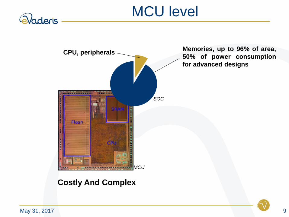
MCU level
May 31, 2017 9
CPU, peripheralsMemories, up to 96% of area,
50% of power consumption
for advanced designs
MCU
SOC
Costly And Complex
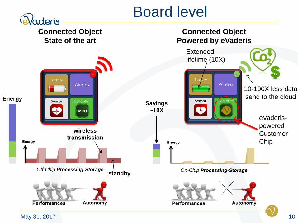
Board level
May 31, 2017 10
BatteryWireless
Sensor Controller
Connected Object
State of the art
On-Chip Processing-Storage
Energy
Performances Autonomy
MCU
BatteryWireless
Sensor Controller
Connected Object
Powered by eVaderis
10-100X less data
send to the cloud
Extended
lifetime (10X)
eVaderis-
powered
Customer
Chip
EnergySavings
~10X
10%Performances Autonomy
Energy
Off-Chip Processing-Storage
wireless
transmission
standby

THE TECHNOLOGY
THE COMPANY
Summary
May 31, 2017 11
THE CONTEXT
THE SYSTEM
THE CO-DEVELOPMENT
CONCLUSION

eFlash/eEE eSRAM eSTTRAM eRRAM (Ox)
Non-volatile Yes No Yes Yes
Compatible with
front end logicNo
FinFET, FDSOIYes Yes Yes
Scalable Sub-28nm ? Yes (size?) Yes Yes
Cell size (density F2) 10-30 (>30 for eEE) 60-80 (HD/LP) 10-30 10-20
Access time 10-100ns(not destructive)
<1ns(not destructive)
2-10ns(not destructive)
10ns(not destructive)
Write/erase processbyte/block/page
levelbit level bit level bit level
Write/erase time1us/10ms (erase)
(page, byte level)<1ns
2-10ns
(bit level)
10-50ns
(bit level)
Endurance 105-106 >1016 1010-1015 107-109
Array standby current 0 1-10µA/Mb(25C) 0 0
Memory comparison 1/3
May 31, 2017 12
eFlash/eEE eSRAM eSTTRAM
Non-volatile Yes No Yes
Compatible with
front end logicNo
FinFET, FDSOIYes Yes
Scalable Sub-28nm ? Yes (size?) Yes
Cell size (density F2) 10-30 (>30 for eEE) 60-80 (HD/LP) 10-30
Access time 10-100ns(not destructive)
<1ns(not destructive)
2-10ns(not destructive)
Write/erase processbyte/block/page
levelbit level bit level
Write/erase time1us/10ms (erase)
(page, byte level)<1ns
2-10ns
(bit level)
Endurance 105-106 >1016 1010-1015
Array standby current 0 1-10µA/Mb(25C) 0
eFlash/eEE eSRAM
Non-volatile Yes No
Compatible with
front end logicNo
FinFET, FDSOIYes
Scalable Sub-28nm ? Yes (size?)
Cell size (density F2) 10-30 (>30 for eEE) 60-80 (HD/LP)
Access time 10-100ns(not destructive)
<1ns(not destructive)
Write/erase processbyte/block/page
levelbit level
Write/erase time1us/10ms (erase)
(page, byte level)<1ns
Endurance 105-106 >1016
Array standby current 0 1-10µA/Mb(25C)
eFlash/eEE
Non-volatile Yes
Compatible with
front end logicNo
FinFET, FDSOI
Scalable Sub-28nm ?
Cell size (density F2) 10-30 (>30 for eEE)
Access time 10-100ns(not destructive)
Write/erase processbyte/block/page
level
Write/erase time1us/10ms (erase)
(page, byte level)
Endurance 105-106
Array standby current 0

Memory comparison 2/3
May 31, 2017 13
• Storage energy @ constant data (1Mb/1s)
t
t
A
A
MRAM
SRAM
Writing NOR
Writing MRAM
(20-25µA/Mb)Leakage SRAMWriting SRAM
• MRAM vs. SRAM:
– 100x more energy for writing in MRAM
– 0 leakage at standby mode (MRAM off)
– ~4x less area MRAM
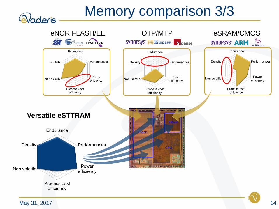
Memory comparison 3/3
May 31, 2017 14
eNOR FLASH/EE eSRAM/CMOSOTP/MTP
Versatile eSTTRAM

STT-RAM Design Space
May 31, 2017 15
MTJ process
MTJ process Fast/LP Write Fast/LP Read Nominal Med Ret/T° High Ret/T°
Diameter (sizing) LOW LOW LOW LOW HIGH
Retention (Ic) LOW MED MED HIGH HIGH
Planar polarizer YES MED MED NO NO
Damping LOW MED MED HIGH HIGH
RA/TMR LOW HIGH MED HIGH MED
STT Register
Multi-bits
Logic synthesis friendly
Area (peripherals) optimized
Restore or save optimized
HP STTRAM
R/W speed optimized
HD STTRAM
Area optimized
Access time optimized
Write power optimized (in
case of data storage)
Architectures
(design param.)
Many process and architectures tradeoff are possible

THE SYSTEM
THE COMPANY
Summary
May 31, 2017 16
THE CONTEXT
THE TECHNOLOGY
THE CO-DEVELOPMENT
CONCLUSION
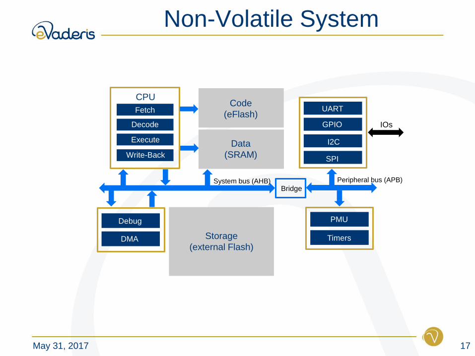
Non-Volatile System
May 31, 2017 17
Fetch
Decode
Execute
Write-Back
CPUCode
(eFlash)
Data
(SRAM)
Storage
(external Flash)
PMU
Timers
BridgeSystem bus (AHB) Peripheral bus (APB)
UART
GPIO
I2C
SPI
IOs
Debug
DMA

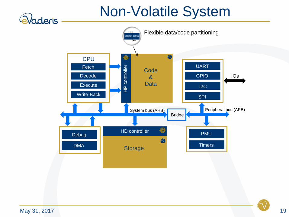
Non-Volatile System
May 31, 2017 18
Fetch
Decode
Execute
Write-Back
CPU
PMU
Timers
BridgeSystem bus (AHB) Peripheral bus (APB)
UART
GPIO
I2C
SPI
IOs
Debug
DMA
Flexible data/code partitioning
Code
&
Data
HP
co
ntr
olle
r
Storage
(external Flash)
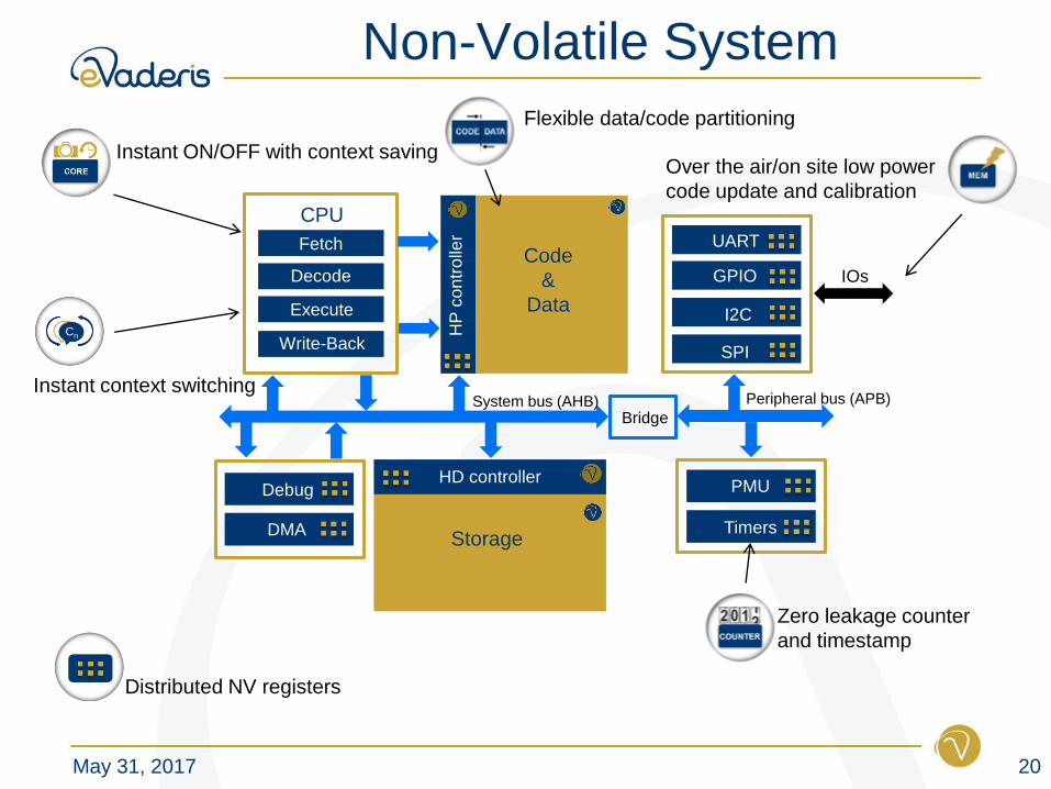
Non-Volatile System
May 31, 2017 19
Fetch
Decode
Execute
Write-Back
CPU
PMU
Timers
BridgeSystem bus (AHB) Peripheral bus (APB)
UART
GPIO
I2C
SPI
IOs
Debug
DMA
Flexible data/code partitioning
Code
&
Data
HP
co
ntr
olle
r
Storage
HD controller
Non-Volatile System
May 31, 2017 20
Fetch
Decode
Execute
Write-Back
CPU
PMU
Timers
BridgeSystem bus (AHB) Peripheral bus (APB)
UART
GPIO
I2C
SPI
IOs
Debug
DMA
Flexible data/code partitioning
Code
&
Data
HP
co
ntr
olle
r
Storage
HD controller
Distributed NV registers
Instant ON/OFF with context saving
Zero leakage counter
and timestamp
Over the air/on site low power
code update and calibration
Cn
Instant context switching

• Increase battery life
– Instant ON/OFF minimize SoC
boot energy loss
– Normally-OFF no idle power
consumption (power down)
• Intermittent power supply support
– Harvesting
– Avoid rollback
• Simplify sleep modes simplify
code dev.
• Simplify code maintenance
– Flexible memory partitioning
– Update over-the-air
• Multi-application support
– Instant context switching
– Reduced context saving overhead
NVP & NVS advantages
May 31, 2017 21

NV CPU and System
May 31, 2017 22
Check
BOOT_ST
Power ON / Reset
Begin User
Application
Continue User
Application
NULL
TRUE Reset
CURRENT
Power OFF
INST_ONRestore Context
BOOT_ST=NULLINST_ON_IRQ
From NV
(memory, register)
All or partial processing states?
Include configuration states
INST_OFF_IRQ
Save Context
BOOT_ST=INST_ON
To NV
(memory, register)
Selective/Compression
Architecture states
(I/D mem, PC, RF).
Microarchitecture states
(pipe, RoB, queue, map table…)
Periodically
On demand
(power fail, context change)

SW retention state
May 31, 2017 23
Boot status
State backup
Exec stack
Reset
Program
Stack pointer
Boot
QMEM
CPU
Update boot status
Write context into
the stack (GPRs,
SPR etc…)
+ Minimal HW impact
- Requires an API more validation
- Requires memory protection
- Energy cost state dependent
- Duration state dependent Not suitable for RT applications
- Complications with caches

• Existing approaches:
– Retention FF: most efficient but largest
– Scan-chain based approach:
• uses existing scan-chain hardware
• minimal area cost but slow and more power consuming
• Complex (flow/dft)
– Drowsy state retention:
• freeze and reduce voltage
• lowest area cost but least efficient
• Complex power management (analog)
• Limitations:– Leakage overhead
– Not power failure tolerant
– Area overhead
– HW impact + controller extra verification
HW Retention state
May 31, 2017 24

• Our approach: NV-FF (extend Retention FF)
• Advantages over existing approach:
– Limited area overhead
– No extra leakage
– Power failure tolerant
• Partial vs Full replacement
– Reduces area and energy overhead
– Requires detailed knowledge of the design
Find best trade-off
HW Retention state
May 31, 2017 25
VDDA
VDD
SAVE
D
VSSA
VSS
RESTORE
Q
VDD
SAVE
D
VSS
RESTORE
Q
VDD
D
VSS
Q
Retention FF NV FF
Ret. FF replacement
NV FF
Low activity profile
Cost Complexity
Efficiency

THE CO-DEVELOPMENT
THE COMPANY
Summary
May 31, 2017 26
THE CONTEXT
THE TECHNOLOGY
THE SYSTEM
CONCLUSION
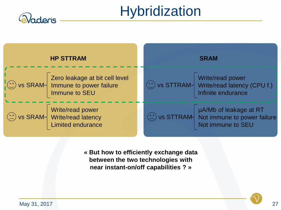
Hybridization
May 31, 2017 27
Zero leakage at bit cell level
Immune to power failure
Immune to SEU
Write/read power
Write/read latency
Limited endurance
vs SRAM
vs SRAM
HP STTRAM
Write/read power
Write/read latency (CPU f.)
Infinite endurance
µA/Mb of leakage at RT
Not immune to power failure
Not immune to SEU
vs STTRAM
vs STTRAM
SRAM
« But how to efficiently exchange data
between the two technologies with
near instant-on/off capabilities ? »

NVSRAM
May 31, 2017 28
Dynamic Static
CPU
CPU
STT-MRAM
SRAMStandbyON

NVSRAM level
May 31, 2017 29
Hybridization at
bit cell level
Hybridization at
IP level
Hybridization at
system level
Massives parallels (save/restore) transfers (fast)
Energy-efficient transfers
The largest area / SRAM bit cell/array adaptation
Impact on SRAM read/write power and latency
Significant parallels (save/restore) transfers (fast)
Energy-efficient transfers
The smallest area
No impact on SRAM
Limited parallels (save/restore) transfers (slow)
Not energy-efficient transfers / complex routing
Acceptable area
No impact on SRAM

NVSRAM architecture
May 31, 2017 30
System Bus: access to SRAM only (hidden STTRAM), CPU/logic frequency
Internal Wide Bus:
• Transfers between SRAM and
STTRAM
• Asynchronous
• Low power
• High bandwith
start@ size

NVSRAM
10 20 30 40 50
1
0.1
0.01
10
100
smartphone
100x to 1000x higher
endurance than MRAM
IoT
<0.5%
Memory size: 2048kB
Cache size: 128kB
SRAM: 1pA/cell
MRAM: 100µA@100ns
TT/25C
May 31, 2017 31

CONCLUSION
THE COMPANY
Summary
May 31, 2017 32
THE CONTEXT
THE TECHNOLOGY
THE SYSTEM
THE CO-DEVELOPMENT

Conclusion
May 31, 2017 33
THE TECHNOLOGY
THE SYSTEM
THE CO-DEVELOPMENT
• Non-Volatile
• Power efficient
• Flexible
• Normally-OFF
• Instant ON/OFF
• Hybrid memory
• Increase efficiency
Find the best trade-off for the application