MAX4684/MAX4685-0.5Ω/0.8Ω Low-Voltage, Dual SPDT Analog ...
10
General Description The MAX4684/MAX4685 low on-resistance (R ON ), low- voltage, dual single-pole/double-throw (SPDT) analog switches operate from a single +1.8V to +5.5V supply. The MAX4684 features a 0.5Ω (max) R ON for its NC switch and a 0.8Ω (max) R ON for its NO switch at a +2.7V supply. The MAX4685 features a 0.8Ω max on-resistance for both NO and NC switches at a +2.7V supply. Both parts feature break-before-make switching action (2ns) with t ON = 50ns and t OFF = 40ns at +3V. The digital logic inputs are 1.8V logic-compatible with a +2.7V to +3.3V supply. The MAX4684/MAX4685 are packaged in the chipscale package (UCSP)™, significantly reducing the required PC board area. The chip occupies only a 2.0mm x 1.50mm area. The 4 x 3 array of solder bumps are spaced with a 0.5mm bump pitch. Applications ● Speaker Headset Switching ● MP3 Players ● Power Routing ● Battery-Operated Equipment ● Relay Replacement ● Audio and Video Signal Routing ● Communications Circuits ● PCMCIA Cards ● Cellular Phones ● Modems Benefits and Features ● 12-Bump, 0.5mm-Pitch UCSP ● NC Switch R ON • 0.5Ω max (+2.7V Supply) (MAX4684) • 0.8Ω max (+2.7V Supply) (MAX4685) ● NO Switch R ON • 0.8Ω max (+2.7V Supply) ● R ON Match Between Channels • 0.06Ω (max) ● R ON Flatness Over Signal Range • 0.15Ω (max) ● +1.8V to +5.5V Single-Supply Operation ● Rail-to-Rail Signal Handling ● 1.8V Logic Compatibility ● Low Crosstalk: -68dB (100kHz) ● High Off-Isolation: -64dB (100kHz) ● THD: 0.03% ● 50nA (max) Supply Current ● Low Leakage Currents • 1nA (max) at T A = +25°C 19-1977; Rev 5; 10/19 UCSP is a trademark of Maxim Integrated Products, Inc. μMAX is a registered trademark of Maxim Integrated Products, Inc. Ordering Information appears at end of data sheet. MAX4684/MAX4685 0.5Ω/0.8Ω Low-Voltage, Dual SPDT Analog Switches in UCSP Click here for production status of specific part numbers.
Transcript of MAX4684/MAX4685-0.5Ω/0.8Ω Low-Voltage, Dual SPDT Analog ...
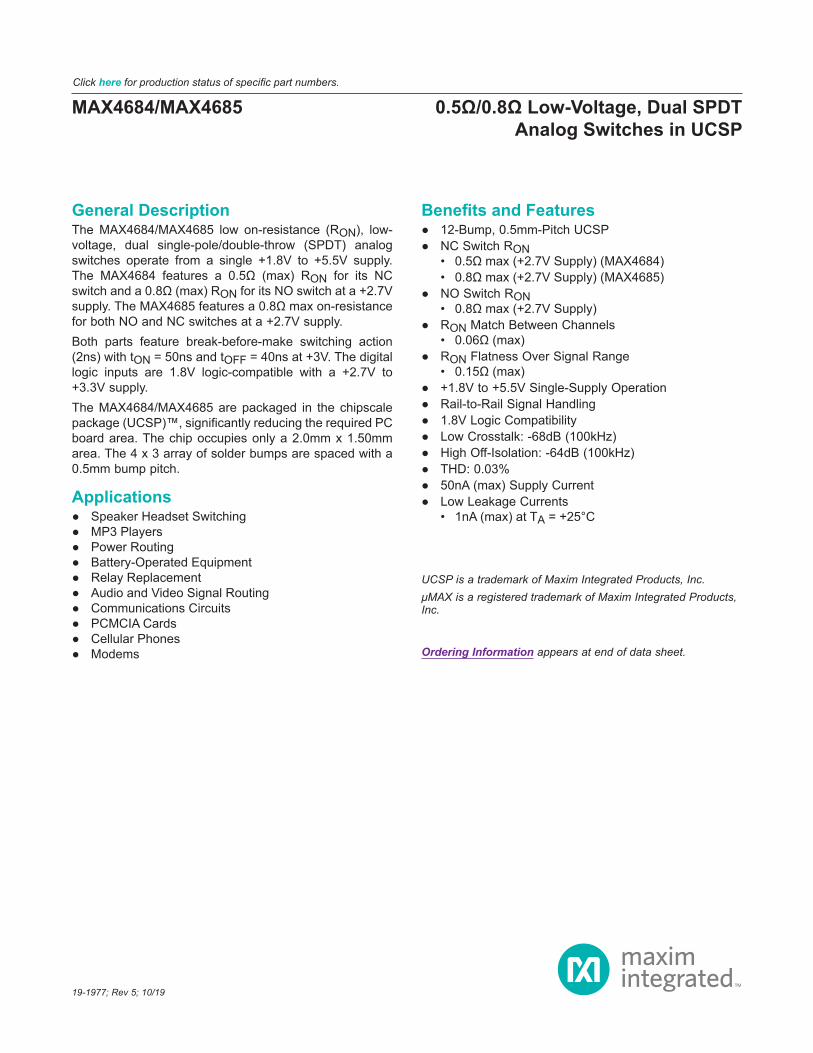
General DescriptionThe MAX4684/MAX4685 low on-resistance (RON), low-voltage, dual single-pole/double-throw (SPDT) analog switches operate from a single +1.8V to +5.5V supply. The MAX4684 features a 0.5Ω (max) RON for its NC switch and a 0.8Ω (max) RON for its NO switch at a +2.7V supply. The MAX4685 features a 0.8Ω max on-resistance for both NO and NC switches at a +2.7V supply.Both parts feature break-before-make switching action (2ns) with tON = 50ns and tOFF = 40ns at +3V. The digital logic inputs are 1.8V logic-compatible with a +2.7V to +3.3V supply.The MAX4684/MAX4685 are packaged in the chipscale package (UCSP)™, significantly reducing the required PC board area. The chip occupies only a 2.0mm x 1.50mm area. The 4 x 3 array of solder bumps are spaced with a 0.5mm bump pitch.
Applications Speaker Headset Switching MP3 Players Power Routing Battery-Operated Equipment Relay Replacement Audio and Video Signal Routing Communications Circuits PCMCIA Cards Cellular Phones Modems
Benefits and Features 12-Bump, 0.5mm-Pitch UCSP NC Switch RON
• 0.5Ω max (+2.7V Supply) (MAX4684)• 0.8Ω max (+2.7V Supply) (MAX4685)
NO Switch RON• 0.8Ω max (+2.7V Supply)
RON Match Between Channels• 0.06Ω (max)
RON Flatness Over Signal Range• 0.15Ω (max)
+1.8V to +5.5V Single-Supply Operation Rail-to-Rail Signal Handling 1.8V Logic Compatibility Low Crosstalk: -68dB (100kHz) High Off-Isolation: -64dB (100kHz) THD: 0.03% 50nA (max) Supply Current Low Leakage Currents
• 1nA (max) at TA = +25°C
19-1977; Rev 5; 10/19
UCSP is a trademark of Maxim Integrated Products, Inc.μMAX is a registered trademark of Maxim Integrated Products, Inc.
Ordering Information appears at end of data sheet.
MAX4684/MAX4685 0.5Ω/0.8Ω Low-Voltage, Dual SPDT Analog Switches in UCSP
Click here for production status of specific part numbers.
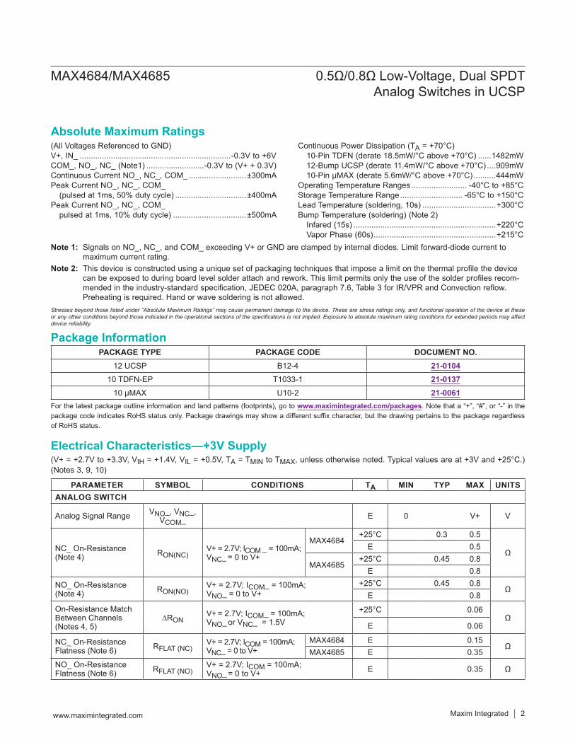
(All Voltages Referenced to GND)V+, IN_ ....................................................................-0.3V to +6VCOM_, NO_, NC_ (Note1) ..........................-0.3V to (V+ + 0.3V)Continuous Current NO_, NC_, COM_ ..........................±300mAPeak Current NO_, NC_, COM_
(pulsed at 1ms, 50% duty cycle) ................................±400mAPeak Current NO_, NC_, COM_
pulsed at 1ms, 10% duty cycle) .................................±500mA
Continuous Power Dissipation (TA = +70°C) 10-Pin TDFN (derate 18.5mW/°C above +70°C) ......1482mW 12-Bump UCSP (derate 11.4mW/°C above +70°C) ....909mW 10-Pin μMAX (derate 5.6mW/°C above +70°C) ..........444mW
Operating Temperature Ranges ......................... -40°C to +85°CStorage Temperature Range ............................ -65°C to +150°CLead Temperature (soldering, 10s) .................................+300°CBump Temperature (soldering) (Note 2)
Infared (15s) ................................................................+220°C Vapor Phase (60s) .......................................................+215°C
(V+ = +2.7V to +3.3V, VIH = +1.4V, VIL = +0.5V, TA = TMIN to TMAX, unless otherwise noted. Typical values are at +3V and +25°C.) (Notes 3, 9, 10)
Note 1: Signals on NO_, NC_, and COM_ exceeding V+ or GND are clamped by internal diodes. Limit forward-diode current to maximum current rating.
Note 2: This device is constructed using a unique set of packaging techniques that impose a limit on the thermal profile the device can be exposed to during board level solder attach and rework. This limit permits only the use of the solder profiles recom-mended in the industry-standard specification, JEDEC 020A, paragraph 7.6, Table 3 for IR/VPR and Convection reflow.Preheating is required. Hand or wave soldering is not allowed.
PARAMETER SYMBOL CONDITIONS TA MIN TYP MAX UNITSANALOG SWITCH
Analog Signal Range VNO_, VNC_, VCOM_ E 0 V+ V
NC_ On-Resistance (Note 4) RON(NC)
V+ = 2.7V; ICOM _ = 100mA; VNC_ = 0 to V+
MAX4684+25°C 0.3 0.5
ΩE 0.5
MAX4685+25°C 0.45 0.8
E 0.8
NO_ On-Resistance (Note 4) RON(NO)
V+ = 2.7V; ICOM_ = 100mA; VNO_ = 0 to V+
+25°C 0.45 0.8Ω
E 0.8On-Resistance Match Between Channels (Notes 4, 5)
∆RONV+ = 2.7V; ICOM_ = 100mA; VNO_ or VNC_ = 1.5V
+25°C 0.06Ω
E 0.06
NC_ On-Resistance Flatness (Note 6) RFLAT (NC)
V+ = 2.7V; ICOM = 100mA; VNC_ = 0 to V+
MAX4684 E 0.15Ω
MAX4685 E 0.35NO_ On-Resistance Flatness (Note 6) RFLAT (NO)
V+ = 2.7V; ICOM = 100mA; VNO_ = 0 to V+ E 0.35 Ω
PACKAGE TYPE PACKAGE CODE DOCUMENT NO.12 UCSP B12-4 21-0104
10 TDFN-EP T1033-1 21-013710 μMAX U10-2 21-0061
www.maximintegrated.com Maxim Integrated 2
MAX4684/MAX4685 0.5Ω/0.8Ω Low-Voltage, Dual SPDT Analog Switches in UCSP
Absolute Maximum Ratings
Stresses beyond those listed under “Absolute Maximum Ratings” may cause permanent damage to the device. These are stress ratings only, and functional operation of the device at these or any other conditions beyond those indicated in the operational sections of the specifications is not implied. Exposure to absolute maximum rating conditions for extended periods may affect device reliability.
Electrical Characteristics—+3V Supply
Package Information
For the latest package outline information and land patterns (footprints), go to www.maximintegrated.com/packages. Note that a “+”, “#”, or “-” in the package code indicates RoHS status only. Package drawings may show a different suffix character, but the drawing pertains to the package regardless of RoHS status.

(V+ = +2.7V to +3.3V, VIH = +1.4V, VIL = +0.5V, TA = TMIN to TMAX, unless otherwise noted. Typical values are at +3V and +25°C.) (Notes 3, 9, 10)
Note 3: The algebraic convention used in this data sheet is where the most negative value is a minimum and the most positive value a maximum.
Note 4: Guaranteed by design.Note 5: ∆RON = RON(MAX) - RON(MIN), between NC1 and NC2 or between NO1 and NO2.Note 6: Flatness is defined as the difference between the maximum and minimum value of on-resistance as measured over the
specified analog signal ranges.Note 7: Leakage parameters are 100% tested at TA = +85°C, and guaranteed by correlation over rated temperature range.Note 8: Off-isolation = 20log10 (VCOM / VNO), VCOM = output, VNO = input to off switch.Note 9: UCSP and TDFN parts are 100% tested at +25°C only and guaranteed by design and correlation at the full hot-rated
temperature.Note 10: -40°C specifications are guaranteed by design.
PARAMETER SYMBOL CONDITIONS TA MIN TYP MAX UNITSNO_ or NC_ Off-Leakage Current (Note 7)
INO_(OFF) or INC_(OFF)
V+ = 3.3V; VNO_ or VNC_ = 3V, 0.3V; VCOM_ = 0.3V, 3V
+25°C -1 1nAE -10 10
COM_ On-Leakage Current (Note 7) ICOM_(ON)
V+ = 3.3V; VNO_ or VNC_ = 3V, 0.3V, or unconnected; VCOM_ = 3V, 0.3V, or unconnected
+25°C -2 2nA
E -20 20
DYNAMIC CHARACTERISTICS
Turn-On Time tONV+ = 2.7V, VNO_ or VNC_ = 1.5V; RL = 50Ω; CL = 35pF; Figure 2
+25°C 30 50ns
E 60
Turn-Off Time tOFFV+ = 2.7V, VNO_ or VNC_ = 1.5V; RL = 50Ω; CL = 35pF; Figure 2
+25°C 25 30ns
E 40
Break-Before-Make Delay tBBM
V+ = 2.7V, VNO_, or VNC_ = 1.5V; RL = 50Ω; CL = 35pF; Figure 3 E 2 15 ns
Charge Injection Q COM_ = 0; RS = 0; CL = 1nF; Figure 4 +25°C 200 pC
Off-Isolation (Note 8) VISOCL = 5pF; RL = 50Ω; f = 100kHz; VCOM_ = 1VRMS; Figure 5 +25°C -64 dB
Crosstalk VCTCL = 5pF; RL = 50Ω; f = 100kHz; VCOM_ = 1VRMS; Figure 5 +25°C -68 dB
Total Harmonic Distortion THD RL = 600Ω, IN_ = 2Vp-p, f = 20Hz to
20kHz +25°C 0.03 %
NC_ Off-Capacitance CNC_(OFF) f = 1MHz; Figure 6 +25°C 84 pFNO_ Off-Capacitance CNO_(OFF) f = 1MHz; Figure 6 +25°C 37 pFNC_ On-Capacitance CNC_(ON) f = 1MHz; Figure 6 +25°C 190 pFNO_ On-Capacitance CNO_(ON) f = 1MHz; Figure 6 +25°C 150 pFDIGITAL I/OInput Logic High VIH E 1.4 VInput Logic Low VIL E 0.5 V
IN_ Input Leakage Current IIN_ VIN_ = 0 or V+
MAX4684/MAX4685E
-1000 +1000nA
MAX4684A -20 +20POWER SUPPLYPower-Supply Range V+ E 1.8 5.5 V
Supply Current (Note 4) I+ V+ = 5.5V; VIN_ = 0 or V++25°C -50 0.04 50
nAE -200 200
www.maximintegrated.com Maxim Integrated 3
MAX4684/MAX4685 0.5Ω/0.8Ω Low-Voltage, Dual SPDT Analog Switches in UCSP
Electrical Characteristics—+3V Supply (continued)
(TA = +25°C, unless otherwise noted.)
MAX4685NC ON-RESISTANCE vs. COM VOLTAGE
0
0.2
0.4
0.6
0.8
1.2
1.4
1.8
1.0
1.6
2.0
0 21 3 4 5
R ON
(Ω)
MAX
4684
/5 to
c02
VCOM (V)
V+ = +5.0V
V+ = +2.3V
V+ = +3.0V
V+ = +1.8V
V+ = +2.0V
V+ = +2.5V
0.10
0.15
0.20
0.25
0.30
0.35
0.40
0.45
0 1 2 3 4 5
MAX
4684
/5 to
c05
MAX4685NC ON-RESISTANCE vs. COM VOLTAGE
VCOM (V)
R ON
(Ω)
V+ = +5V
TA = +25°CTA = -40°C
TA = +85°C
0.15
0.10
0.20
0.25
0.30
0.35
0.40
0.45
0.50
0 1.00.5 1.5 2.0 2.5 3.0
MAX
4684
/5 to
c08
MAX4685NC ON-RESISTANCE vs. COM VOLTAGE
VCOM (V)
R ON
(Ω)
V+ = +3V
TA = +85°C
TA = +25°C
TA = -40°C
NO ON-RESISTANCE vs. COM VOLTAGE
0
0.5
1.5
1.0
2.0
2.5
0 21 3 4 5
R ON
(Ω)
MAX
4684
/5 to
c03
VCOM (V)
V+ = +5.0V
V+ = +1.8V
V+ = +2.0V
V+ = +2.3VV+ = +2.5V
V+ = +3.0V
0.10
0.15
0.20
0.25
0.30
0.35
0.40
0 1 2 3 4 5
MAX
4684
/5 to
c06
NO ON-RESISTANCE vs. COM VOLTAGE
VCOM (V)
R ON
(Ω) TA = +85°C
V+ = +5V
TA = -40°C
TA = +25°C
0.15
0.10
0.20
0.25
0.30
0.35
0.40
0.45
0.50
0 1.00.5 1.5 2.0 2.5 3.0
MAX
4684
/5 to
c09
NO ON-RESISTANCE vs. COM VOLTAGE
VCOM (V)
R ON
(Ω)
V+ = +3V
TA = +85°C
TA = +25°CTA = -40°C
POSITIVE SUPPLY
COMNO
D1
GND
Vg
V+MAX4684MAX4685
0.10
0.12
0.14
0.16
0.20
0.18
0.22
0.24
0.26
0.28
0 21 3 4 5
MAX
4684
/5 to
c04
MAX4684NC ON-RESISTANCE vs. COM VOLTAGE
VCOM (V)
R ON
(Ω)
TA = +85°C
V+ = +5V
TA = -40°C
TA = +25°C
0 1.0 1.50.5 2.0 2.5 3.00.10
0.15
0.20
0.25
0.30
0.35
MAX
4684
/5 to
c07
MAX4684NC ON-RESISTANCE vs. COM VOLTAGE
VCOM (V)
R ON
(Ω)
V+ = +3V
TA = +85°C
TA = -40°C
TA = +25°C
Maxim Integrated 4www.maximintegrated.com
MAX4684/MAX4685 0.5Ω/0.8Ω Low-Voltage, Dual SPDT Analog Switches in UCSP
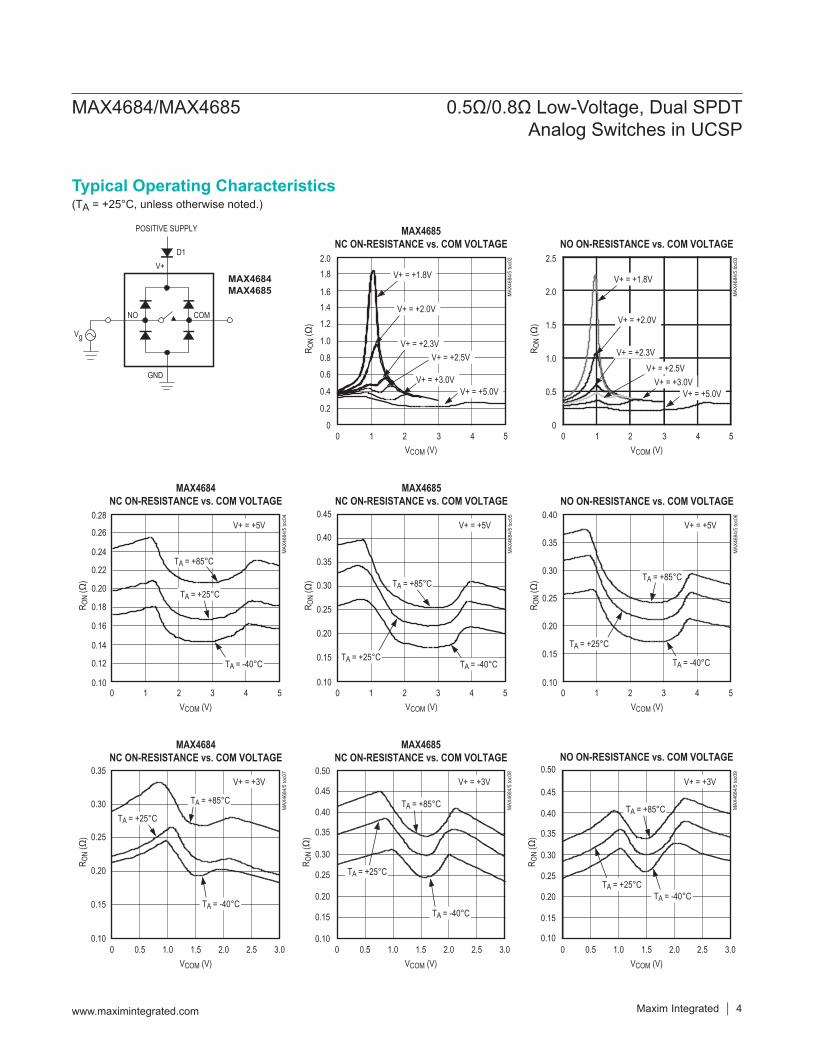
Typical Operating Characteristics
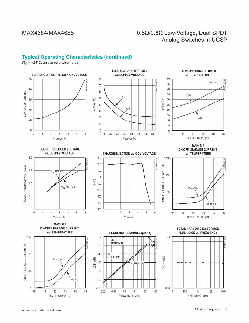
(TA = +25°C, unless otherwise noted.)
0
20
10
40
30
50
60
70
80
1.8 2.8 3.32.3 3.8 4.3 4.8 5.3
MAX
4684
/5 to
c11
VSUPPLY (V)
t ON/
t OFF
(ns)
TURN-ON/TURN-0FF TIMESvs. SUPPLY VOLTAGE
tON
tOFF
-500
-400
-300
-200
-100
0
100
200
300
0 21 3 4 5 6
CHARGE INJECTION vs. COM VOLTAGEM
AX46
84/5
toc1
4
Q (p
C)
VCOM (V)
FREQUENCY RESPONSE (µMAX)
FREQUENCY (MHz)0.001 1 10 1000.01 0.1
LOSS
(dB)
-120
-100
-80
-20
-40
-60
0
MAX
4684
/85
toc1
7
ON-RESPONSE
OFF-ISOLATION
CROSSTALK
0
15
10
5
20
25
30
35
40
45
50
-40 10-15 35 60 85
MAX
4684
/5 to
c12
TURN-ON/TURN-0FF TIMESvs. TEMPERATURE
V+ = +3V
t ON/
t OFF
(ns)
TEMPERATURE (°C)
tON
tOFF
-40 10-15 35 60 85
MAX
4684
/5 to
c15
TEMPERATURE (°C)
ON/O
FF-L
EAKA
GE C
URRE
NT (p
A)
1
10
100
1000
MAX4684ON/OFF-LEAKAGE CURRENT
vs. TEMPERATURE
ICOM(ON)
ICOM(OFF)
10 100 1k 10k 100k
TOTAL HARMONIC DISTORTIONPLUS NOISE vs. FREQUENCY
MAX
4684
/5 to
c18
FREQUENCY (Hz)
THD
+ N
(%)
0.01
0.1
0
20
60
40
80
100
0 21 3 4 5 6
SUPPLY CURRENT vs. SUPPLY VOLTAGE
MAX
4684
/5 to
c10
VSUPPLY (V)
SUPP
LY C
URRE
NT (p
A)
2.0
1.5
1.0
0.5
00 31 2 4 5 6
LOGIC THRESHOLD VOLTAGEvs. SUPPLY VOLTAGE
MAX
4684
/5 to
c13
LOGI
C TH
RESH
OLD
VOLT
AGE
(V)
VSUPPLY (V)
VIN RISING
VIN FALLING
-40 10-15 35 60 85
MAX
4684
/5 to
c16
TEMPERATURE (°C)
ON/O
FF-L
EAKA
GE C
URRE
NT (p
A)
1
10
100
1000
MAX4685ON/OFF-LEAKAGE CURRENT
vs. TEMPERATURE
ICOM(ON)
ICOM(OFF)
Maxim Integrated 5www.maximintegrated.com
MAX4684/MAX4685 0.5Ω/0.8Ω Low-Voltage, Dual SPDT Analog Switches in UCSP
Typical Operating Characteristics (continued)
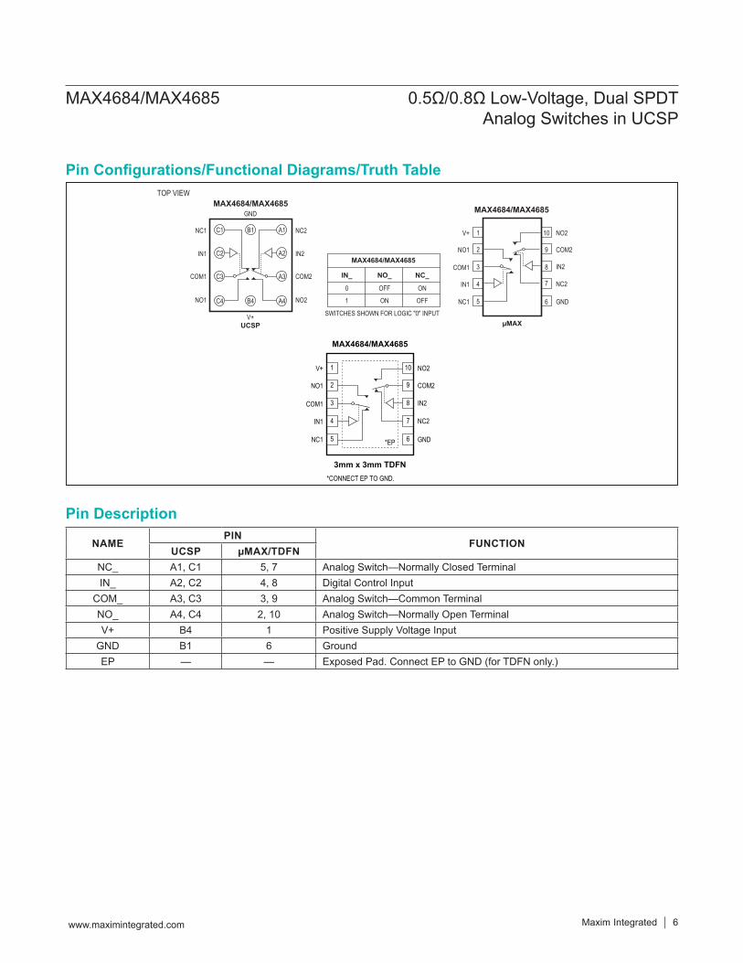
NAMEPIN
FUNCTIONUCSP µMAX/TDFN
NC_ A1, C1 5, 7 Analog Switch—Normally Closed TerminalIN_ A2, C2 4, 8 Digital Control Input
COM_ A3, C3 3, 9 Analog Switch—Common TerminalNO_ A4, C4 2, 10 Analog Switch—Normally Open TerminalV+ B4 1 Positive Supply Voltage Input
GND B1 6 GroundEP — — Exposed Pad. Connect EP to GND (for TDFN only.)
COM2COM1
NO2NO1
NC2
IN2IN1
NC1
GND
V+
TOP VIEW
IN_
0
1
NO_
MAX4684/MAX4685
OFF
ON
NC_
ON
SWITCHES SHOWN FOR LOGIC "0" INPUT
OFF
UCSP
MAX4684/MAX4685MAX4684/MAX4685
NC2IN1
GNDNC1
2
3
9
8
COM2
IN2COM1
NO1
1 10 NO2V+
4
5
7
6
µMAX
C1
C2
C3
C4 B4 A4
A3
A2
A1B1
TOP VIEW
NC2IN1
GNDNC1
COM2
IN2COM1
NO1
NO2V+
3mm x 3mm TDFN
9
8
10
7
6
*CONNECT EP TO GND.
2
3
1
4
5 *EP
MAX4684/MAX4685
Pin Configurations/Functional Diagrams/Truth Table
www.maximintegrated.com Maxim Integrated 6
MAX4684/MAX4685 0.5Ω/0.8Ω Low-Voltage, Dual SPDT Analog Switches in UCSP
Pin Description

Detailed DescriptionThe MAX4684/MAX4685 are low on-resistance, low-voltage, dual SPDT analog switches that operate from a +1.8V to +5.5V supply. The devices are fully specified for nominal 3V applications. The MAX4684/MAX4685 have break-before-make switching and fast switching speeds (tON = 50ns max, tOFF = 40ns max).The MAX4684 offers asymmetrical normally closed (NC) and normally open (NO) RON for applications that require asymmetrical loads (examples include speaker headsets and internal speakers). The part features a 0.5Ω max RON for its NC switch and a 0.8Ω max RON for its NO switch at the 2.7V supply. The MAX4685 features a 0.8Ω max on-resistance for both NO and NC switches at the +2.7V supply.
Applications InformationDigital Control InputsThe MAX4684/MAX4685 logic inputs accept up to +5.5V regardless of supply voltage. For example, with a +3.3V supply, IN_ may be driven low to GND and high to 5.5V. Driving IN_ rail-to-rail minimizes power consumption. Logic levels for a +1.8V supply are 0.5V (low) and 1.4V (high).
Analog Signal LevelsAnalog signals that range over the entire supply voltage (V+ to GND) are passed with very little change in on-resistance (see Typical Operating Characteristics). The switches are bidirectional, so the NO_, NC_, and COM_ pins can be either inputs or outputs.
Power-Supply Sequencing and Overvoltage ProtectionCaution: Do not exceed the absolute maximum rat-ings because stresses beyond the listed ratings may cause permanent damage to devices.Proper power-supply sequencing is recommended for all CMOS devices. Always apply V+ before applying analog signals, especially if the analog signal is not current lim-ited. If this sequencing is not possible, and if the analog inputs are not current limited to <20mA, add a small sig-nal diode (D1) as shown in Figure 1. Adding a protection diode reduces the analog range to a diode drop (about 0.7V) below V+ (for D1). RON increases slightly at low
supply voltages. Maximum supply voltage (V+) must not exceed +6V. Protection diode D1 also protects against some overvoltage situations. No damage will result on Figure 1’s circuit if the supply voltage is below the abso-lute maximum rating applied to an analog signal pin.
UCSP Package ConsiderationFor general UCSP package information and PC layout considerations, please refer to the Maxim Application Note (Wafer-Level Ultra-Chip-Board-Scale Package).
UCSP ReliabilityThe chip-scale package (UCSP) represents a unique packaging form factor that may not perform equally to a packaged product through traditional mechanical reliabil-ity tests. UCSP reliability is integrally linked to the user’s assembly methods, circuit board material, and usage environment. The user should closely review these areas when considering use of a UCSP package. Performance through Operating Life Test and Moisture Resistance remains uncompromised as it is primarily determined by the wafer-fabrication process.Mechanical stress performance is a greater consideration for a UCSP package. UCSPs are attached through direct solder contact to the user’s PC board, foregoing the inher-ent stress relief of a packaged product lead frame. Solder joint contact integrity must be considered. Information on Maxim’s qualification plan, test data, and recommendations are detailed in the UCSP application note, which can be found on Maxim’s website at www.maximintegrated.com.
Figure 1. Overvoltage Protection Using Two External Blocking Diodes
POSITIVE SUPPLY
COMNO
D1
GND
Vg
V+MAX4684MAX4685
www.maximintegrated.com Maxim Integrated 7
MAX4684/MAX4685 0.5Ω/0.8Ω Low-Voltage, Dual SPDT Analog Switches in UCSP

Figure 2. Switching Time
Figure 3. Break-Before-Make Interval
Figure 4. Charge Injection
tr < 5nstf < 5ns
50%VIL
LOGICINPUT
RL50Ω
COM_
GND
IN_
CL INCLUDES FIXTURE AND STRAY CAPACITANCE.
VOUT = VN_ ( RL ) RL + RON
VIN_
VIH
tOFF
0
NO_OR NC
0.9 x V0UT 0.9 x VOUT
tON
VOUT
SWITCHOUTPUT
LOGICINPUT
LOGIC INPUT WAVEFORMS INVERTED FOR SWITCHESTHAT HAVE THE OPPOSITE LOGIC SENSE.
V+
CL35pF
V+
VOUT
MAX4684MAX4685
50%VIH
VIL
LOGICINPUT
VOUT 0.9 x VOUT
tD
LOGICINPUT
RL50Ω
GND
CL INCLUDES FIXTURE AND STRAY CAPACITANCE.
NO_
IN_
NC_ VOUT
V+
V+
CL35pF
VN_ COM_
MAX4684MAX4685
VGENGND
COM_
CL
VOUT
V+ VOUT
INOFF
ONOFF
∆VOUT
Q = (∆VOUT)(CL)
NC_
IN DEPENDS ON SWITCH CONFIGURATION;INPUT POLARITY DETERMINED BY SENSE OF SWITCH.
OFFON
OFFIN
VIL TO VIH
V+
RGEN
IN_
MAX4684MAX4685
OR NO_
www.maximintegrated.com Maxim Integrated 8
MAX4684/MAX4685 0.5Ω/0.8Ω Low-Voltage, Dual SPDT Analog Switches in UCSP
Test Circuits/Timing Diagrams

Figure 5. On-Loss, Off-Isolation, and Crosstalk
Figure 6. Channel Off/On-Capacitance
+Denotes a lead(Pb)-free/RoHS-compliant package.Note: Requires special solder temperature profile described in the Absolute Maximum Ratings section.*UCSP reliability is integrally linked to the user’s assembly methods, circuit board material, and environment. Refer to the UCSP Reliability Notice in the UCSP Reliability section of this data sheet for more information.**EP = Exposed PadT = Tape and reel.
PART TEMP RANGE PIN/BUMP-PACKAGE
TOP MARK
MAX4684EBC+T -40°C to +85°C 12 UCSP* AAFMAX4684ETB+T -40°C to +85°C 10 TDFN-EP** AAGMAX4684EUB+T -40°C to +85°C 10 µMAX® —MAX4684AEBC+T -40°C to +85°C 12 UCSP* AEJMAX4685EBC+T -40°C to +85°C 12 UCSP* AAGMAX4685ETB+T -40°C to +85°C 10 TDFN-EP** AAHMAX4685EUB+T -40°C to +85°C 10 µMAX —
MEASUREMENTS ARE STANDARDIZED AGAINST SHORTS AT IC TERMINALS. OFF-ISOLATION IS MEASURED BETWEEN COM_ AND "OFF" NO_ OR NC_ TERMINAL ON EACH SWITCH. ON-LOSS IS MEASURED BETWEEN COM_ AND "ON" NO_ OR NC_ TERMINAL ON EACH SWITCH. CROSSTALK IS MEASURED FROM ONE CHANNEL TO ALL OTHER CHANNELS.SIGNAL DIRECTION THROUGH SWITCH IS REVERSED; WORST VALUES ARE RECORDED.
+5V
VOUT
V+IN_
NC_
COM
NO
VIN
MAX4684MAX4685
OFF-ISOLATION = 20log VOUT
VIN
ON-LOSS = 20log VOUT
VIN
CROSSTALK = 20log VOUT
VIN
NETWORKANALYZER
50Ω
50Ω 50Ω
50Ω
MEAS REF
10nF
0V OR V+
50Ω
GND
CAPACITANCEMETER NC_ or
NO_
COM_
GND
IN VILORVIH
10nF V+
f = 1MHz
V+MAX4684MAX4685
www.maximintegrated.com Maxim Integrated 9
MAX4684/MAX4685 0.5Ω/0.8Ω Low-Voltage, Dual SPDT Analog Switches in UCSP
Test Circuits/Timing Diagrams (continued)
Ordering Information
Chip InformationPROCESS: BiCMOS

REVISION NUMBER
REVISION DATE DESCRIPTION PAGES
CHANGED3 2/03 Added TDFN packaging, noted parts are now UCSP qualified —4 1/09 Added lead-free packaging and exposed pad note 1, 2, 6–9
5 10/19 Updated the Electrical Characteristics table and added MAX4684AEBC+T to the Ordering Information table 3, 9
Maxim Integrated cannot assume responsibility for use of any circuitry other than circuitry entirely embodied in a Maxim Integrated product. No circuit patent licenses are implied. Maxim Integrated reserves the right to change the circuitry and specifications without notice at any time. The parametric values (min and max limits) shown in the Electrical Characteristics table are guaranteed. Other parametric values quoted in this data sheet are provided for guidance.
Maxim Integrated and the Maxim Integrated logo are trademarks of Maxim Integrated Products, Inc. © 2019 Maxim Integrated Products, Inc. 10
MAX4684/MAX4685 0.5Ω/0.8Ω Low-Voltage, Dual SPDT Analog Switches in UCSP
Revision History
For pricing, delivery, and ordering information, please visit Maxim Integrated’s online storefront at https://www.maximintegrated.com/en/storefront/storefront.html.