
Magnetic Sensor - Microsoft...= 25°C. Parameter Symbol Test Conditions Min Typ Max Unit Vout Output...
13
High Accuracy Current Sensor IC with 1.5MHz 3dB Bandwidth and Isolation ±5A, ±20A, ±50A, 5V, Fixed Gain MCA1101-xx-5 FEATURES AMR based integrated current sensor Superior Range & Accuracy 0.6% typical total error @25°C (MCA1101-20-5) 2.0% max error over temperature (MCA1101-20-5) Superior Frequency Response 1.5 MHz (typical 3dB BW) Fast output response time (300ns typical) Low Primary Resistance (0.9 mΩ) Single 5V Supply Operation Low power consumption (6.5mA typical) Zero-Current Reference Pin (Vref) Overcurrent fault detection SOIC-16 package (RoHS/REACH compliant) -40 to +105°C Operating Temperature Range UL/IEC/EN60950-1 Certified 4.8 kV Dielectric Strength Voltage 1097 VRMS Basic Isolation Voltage 400 VRMS Reinforced Isolation Voltage APPLICATIONS Server, Telecom, & Industrial PWR Supplies Power Aggregation, Over-Current Protection Dynamic Current Sensing in Feedback Loops PFC and Inverter Control Motor Control Loops & Protection Automation, Robotics, Servo Systems Automotive & EV Power Systems Solar Inverters and Optimizers Grid-Tie and Storage Current Monitoring MPPT Circuit Current Monitoring Central Inverter Current Monitoring Consumer Motor Balance and Remote Device Monitoring Home Automation Control & IOT remote sensing DESCRIPTION The MCA1101 products are ±5A, ±20A, ±50A fully integrated bi-directional analog output current sensors that deliver both high accuracy and high bandwidth. ACEINNA’s state-of-the-art Anisotropic Magneto Resistive (AMR) sensor technology provides inherently low noise, excellent linearity and repeatability. A fully isolated current path is provided by a low resistance copper conductor integrated into the package making it suitable for both high-side and low side bi-directional current sensing. The high bandwidth of 1.5MHz (3dB) and low phase delay makes it ideal for current sense feedback loops in motor control, inverters, uninterruptible power supplies, battery management, power factor correction, high voltage distribution bus converters and power supply applications, including those with fast switching wide-bandgap SiC and GaN based power stages. These devices are factory-calibrated to achieve low offset error and provide a precise analog voltage output that is linearly proportional to the conduction current (AC or DC) with sensitivity (mV/A) compatible with A/D converters and analog control loops in power systems. The AMR sensor device structure is designed to eliminate sensitivity to stray and common mode magnetic fields. Due to the inherently low output noise of ACEINNA’s sensor technology, additional filtering is not required to reduce noise that reduces accuracy at low-level currents in systems with dynamic load profiles. The MCA1101 products in SOIC-16 package are simple to use with no or minimal external components (other than decoupling capacitor) enabling fast design, supports high isolation and are UL/IEC/EN60950-1 certified. Figure 1 - Application circuit Information furnished by ACEINNA is believed to be accurate and reliable. However, no responsibility is assumed by ACEINNA for its use, or for any infringements of patents or other rights of third parties which may result from its use. No license is granted by implication or otherwise under any patent or patent rights of ACEINNA. ACEINNA reserves the right to change this specification without notification. Intterupt to MCU To ADC pin on MCU or A/D input Optional circuitry for overcurrent detection R1 R3 R2 33K 10K C1 100nF To ADC pin on MCU or A/D input Primary Current Input Primary Current Output IP+ IP+ IP+ IP+ IP- IP- IP- IP- VOC GND GND Vref Vout GND VCC FAULTB VCC VCC VCC
Transcript of Magnetic Sensor - Microsoft...= 25°C. Parameter Symbol Test Conditions Min Typ Max Unit Vout Output...
High Accuracy Current Sensor IC with 1.5MHz 3dB Bandwidth and Isolation
±5A, ±20A, ±50A, 5V, Fixed Gain
MCA1101-xx-5
FEATURES
AMR based integrated current sensor
Superior Range & Accuracy 0.6% typical total error @25°C (MCA1101-20-5) 2.0% max error over temperature (MCA1101-20-5)
Superior Frequency Response 1.5 MHz (typical 3dB BW)
Fast output response time (300ns typical)
Low Primary Resistance (0.9 mΩ)
Single 5V Supply Operation
Low power consumption (6.5mA typical)
Zero-Current Reference Pin (Vref)
Overcurrent fault detection
SOIC-16 package (RoHS/REACH compliant)
-40 to +105°C Operating Temperature Range
UL/IEC/EN60950-1 Certified 4.8 kV Dielectric Strength Voltage 1097 VRMS Basic Isolation Voltage
400 VRMS Reinforced Isolation Voltage
APPLICATIONS
Server, Telecom, & Industrial PWR Supplies Power Aggregation, Over-Current Protection Dynamic Current Sensing in Feedback Loops PFC and Inverter Control
Motor Control Loops & Protection Automation, Robotics, Servo Systems Automotive & EV Power Systems
Solar Inverters and Optimizers Grid-Tie and Storage Current Monitoring MPPT Circuit Current Monitoring Central Inverter Current Monitoring
Consumer Motor Balance and Remote Device Monitoring Home Automation Control & IOT remote sensing
DESCRIPTION
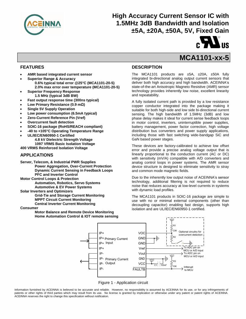
The MCA1101 products are ±5A, ±20A, ±50A fully integrated bi-directional analog output current sensors that deliver both high accuracy and high bandwidth. ACEINNA’s state-of-the-art Anisotropic Magneto Resistive (AMR) sensor technology provides inherently low noise, excellent linearity and repeatability.
A fully isolated current path is provided by a low resistance copper conductor integrated into the package making it suitable for both high-side and low side bi-directional current sensing. The high bandwidth of 1.5MHz (3dB) and low phase delay makes it ideal for current sense feedback loops in motor control, inverters, uninterruptible power supplies, battery management, power factor correction, high voltage distribution bus converters and power supply applications, including those with fast switching wide-bandgap SiC and GaN based power stages.
These devices are factory-calibrated to achieve low offset error and provide a precise analog voltage output that is linearly proportional to the conduction current (AC or DC) with sensitivity (mV/A) compatible with A/D converters and analog control loops in power systems. The AMR sensor device structure is designed to eliminate sensitivity to stray and common mode magnetic fields.
Due to the inherently low output noise of ACEINNA’s sensor technology, additional filtering is not required to reduce noise that reduces accuracy at low-level currents in systems with dynamic load profiles.
The MCA1101 products in SOIC-16 package are simple to use with no or minimal external components (other than decoupling capacitor) enabling fast design, supports high isolation and are UL/IEC/EN60950-1 certified.
Figure 1 - Application circuit
Information furnished by ACEINNA is believed to be accurate and reliable. However, no responsibility is assumed by ACEINNA for its use, or for any infringements of patents or other rights of third parties which may result from its use. No license is granted by implication or otherwise under any patent or patent rights of ACEINNA. ACEINNA reserves the right to change this specification without notification.
Intterupt
to MCU
To ADC pin on
MCU or A/D input
Optional circuitry for
overcurrent detection
R1
R3
R2
33K
10K C1 100nF
To ADC pin on
MCU or A/D input
Primary Current
Input
Primary Current
Output
IP+
IP+
IP+
IP+
IP-
IP-
IP-
IP-
VOC
GND
GND
Vref
Vout
GND
VCC
FAULTB
VCC
VCC
VCC
Phone: 978.965.3200 Fax: 978.965.3201 E-mail: [email protected] www.aceinna.com
Document: 6020-1102-01 Rev D Page 2 of 13
ORDERING PART NUMBER
Ordering Part Number
Part Marking (See Page 12)
Current Range
Gain VCC
(Typical) Dielectric Strength
Package Qty per
Reel
MCA1101-5-5 MCA11055 ±5 Amp Fixed 5.0V 4800V 16 Lead SOIC 1000 pcs
MCA1101-20-5 MCA11205 ±20 Amp Fixed 5.0V 4800V 16 Lead SOIC 1000 pcs
MCA1101-50-5 MCA11505 ±50 Amp Fixed 5.0V 4800V 16 Lead SOIC 1000 pcs
Note: Evaluation boards are available for each product version (order EVB-MCx1101-xx-x)
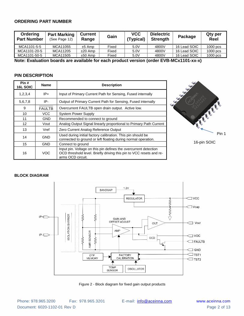
PIN DESCRIPTION
Pin # 16L SOIC
Name Description
1,2,3,4 IP+ Input of Primary Current Path for Sensing, Fused internally
5,6,7,8 IP- Output of Primary Current Path for Sensing, Fused internally
9 FAULTB Overcurrent FAULTB open drain output. Active low.
10 VCC System Power Supply
11 GND Recommended to connect to ground
12 Vout Analog Output Signal linearly proportional to Primary Path Current
13 Vref Zero Current Analog Reference Output
14 GND Used during initial factory calibration. This pin should be connected to ground or left floating during normal operation.
15 GND Connect to ground
16 VOC Input pin. Voltage on this pin defines the overcurrent detection OCD threshold level. Briefly driving this pin to VCC resets and re-arms OCD circuit.
BLOCK DIAGRAM
Figure 2 - Block diagram for fixed gain output products
Pin 1
16-pin SOIC
CONFID ENTIAL
Phone: 978.965.3200 Fax: 978.965.3201 E-mail: [email protected] www.aceinna.com
Document: 6020-1102-01 Rev D Page 3 of 13
Table 1 – ABSOLUTE MAXIMUM RATINGS
Stresses above these ratings may cause permanent damage. Exposure to absolute maximum conditions for extended periods may degrade device reliability. These are stress ratings only, and functional operation at these or any other conditions beyond those specified is not implied.
Parameters / Test Conditions Symbol Value Unit
Supply Voltage
VCCMAX -0.5 to 6 V
FAULTB Output Voltage
V FAULTB -0.5V to
VCC+0.5V V
Sensor Current (IP+, IP-), 5Amp products
IPMAX ±10 A
Sensor Current (IP+, IP-), 20Amp products IPMAX ±50 A
Sensor Current (IP+, IP-), 50Amp products IPMAX ±100 A
Maximum Device Junction Temperature TJMAX 150 °C
Storage Temperature TSTG -65 to +150 °C
Operating Ambient Temperature Range TA -40 to 105 °C
ESD Human Body Model / per ANSI/ESDA/JEDEC JS-001 HBM 2000 V
ESD Charged Device Model / per JEDEC specification JESD22-C101 CDM 1500 V
MSL Rating MSL 3
Maximum Soldering Temperature, 10 seconds. TSOLDER 260 °C
CONFID ENTIAL
Phone: 978.965.3200 Fax: 978.965.3201 E-mail: [email protected] www.aceinna.com
Document: 6020-1102-01 Rev D Page 4 of 13
Table 2 – ISOLATION CHARACTERISTICS
Parameters / Test Conditions Symbol Value Unit
Dielectric Strength Test Voltage (Agency type-tested for 60 seconds per UL standard 60950-1 (edition 2). Production tested at 3kVrms per UL 60950-1.
VISO 4800 V
Working Voltage for Basic Isolation. Maximum approved working voltage according to UL 60950-1 (edition 2)- (VPK/DC / VRMS)
VWVBI 1550 / 1097 V
Working Voltage for Reinforced Isolation (VPK/DC / VRMS) VWVRI 565 / 400 V
Clearance distance (Minimum distance through air from IP leads to signal leads) DCL 7.5 mm
Creepage distance (Minimum distance along package body from IP leads to signal leads)
DCR 8.2 mm
Table 3 – THERMAL CHARACTERISTICS
Parameters / Test Conditions Symbol Value Unit
Junction-to-Ambient Thermal Resistance (Note 1) RJA 27 C/W
Junction-to-Lead Thermal Resistance RJC 10 C/W
Note 1 – The RJA measured on the EB0011- evaluation board with 800mm2 of 4oz copper on each layer (top and bottom ), thermal vias connecting the layers. The performance values include the power consumed by the PCB.
Table 4 – ELECTRICAL CHARACTERISTICS COMMON TO ALL VERSIONS
Unless otherwise noted: 4.5V ≤ VCC ≤ 5.5V, -40°C ≤ TA ≤ 105°C, I (Vout) = I (Vref) = 0 (Recommended Operating Conditions). Typical values are for VCC = 5V and TA = 25°C.
Parameter Symbol Test Conditions Min Typ Max Unit
Vout Output
Load Regulation VoutLR Increase I (Vout) from 0 to -250µA. Measure change in Vout voltage
2 4 mV
Source Current VoutSRC Vout shorted to GND 50 mA
Sink Current VoutSNK Vout shorted to VCC 30 mA
Frequency Response (-3dB) VoutBW (Note 2) 1500 kHz
Capacitive Loading CVoutMAX (Note 2) 200 pF
Resistive Loading RLMIN Minimum load resistance on Vout & Vref. (Note 2 and Note 3)
10 kohm
Response Time tRESP IP± = 0 to ±100% step input, interval from 80% of the IP to 80% of the Vout. (Note 2)
300 ns
Noise Density IND Input Referred, VCC=5V, TA = 25°C, CL=200pF, 10 kHz~1MHz
10 µA/Hz
Noise (Input Referred) VoutNOISE IP± = 0, Measure (Vout – Vref). BW defined from DC to 10 kHz. (Note 2)
10 mA
(rms)
Note 2 – Guaranteed by design and characterization. Not production tested. Note 3 – Vref pin supply capability limited to Fixed Gain mode.
CONFID ENTIAL
Phone: 978.965.3200 Fax: 978.965.3201 E-mail: [email protected] www.aceinna.com
Document: 6020-1102-01 Rev D Page 5 of 13
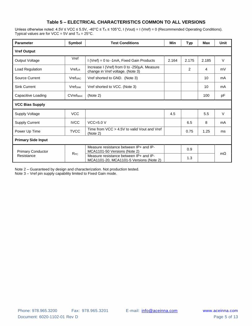
Table 5 – ELECTRICAL CHARACTERISTICS COMMON TO ALL VERSIONS
Unless otherwise noted: 4.5V ≤ VCC ≤ 5.5V, -40°C ≤ TA ≤ 105°C, I (Vout) = I (Vref) = 0 (Recommended Operating Conditions). Typical values are for VCC = 5V and TA = 25°C.
Note 2 – Guaranteed by design and characterization. Not production tested. Note 3 – Vref pin supply capability limited to Fixed Gain mode.
Parameter Symbol Test Conditions Min Typ Max Unit
Vref Output
Output Voltage Vref
I (Vref) = 0 to -1mA, Fixed Gain Products 2.164 2.175 2.185 V
Load Regulation VrefLR Increase I (Vref) from 0 to -250µA. Measure change in Vref voltage. (Note 3)
2 4 mV
Source Current VrefSRC Vref shorted to GND. (Note 3) 10 mA
Sink Current VrefSNK Vref shorted to VCC. (Note 3) 10 mA
Capacitive Loading CVrefMAX (Note 2) 100 pF
VCC Bias Supply
Supply Voltage VCC 4.5 5.5 V
Supply Current IVCC VCC=5.0 V 6.5 8 mA
Power Up Time TVCC Time from VCC > 4.5V to valid Vout and Vref (Note 2)
0.75 1.25 ms
Primary Side Input
Primary Conductor Resistance
RPC
Measure resistance between IP+ and IP- MCA1101-50 Versions (Note 2)
0.9
mΩ Measure resistance between IP+ and IP- MCA1101-20, MCA1101-5 Versions (Note 2)
1.3
CONFID ENTIAL
Phone: 978.965.3200 Fax: 978.965.3201 E-mail: [email protected] www.aceinna.com
Document: 6020-1102-01 Rev D Page 6 of 13
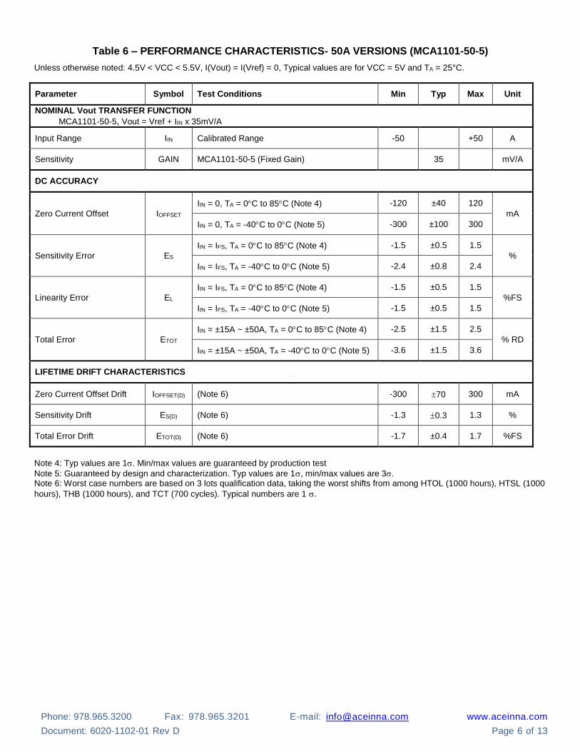
Table 6 – PERFORMANCE CHARACTERISTICS- 50A VERSIONS (MCA1101-50-5)
Unless otherwise noted: 4.5V < VCC < 5.5V, I(Vout) = I(Vref) = 0, Typical values are for VCC = 5V and TA = 25°C.
Parameter Symbol Test Conditions Min Typ Max Unit
NOMINAL Vout TRANSFER FUNCTION MCA1101-50-5, Vout = Vref + IIN x 35mV/A
Input Range IIN Calibrated Range -50 +50 A
Sensitivity GAIN MCA1101-50-5 (Fixed Gain) 35 mV/A
DC ACCURACY
Zero Current Offset IOFFSET
IIN = 0, TA = 0C to 85C (Note 4) -120 ±40 120
mA
IIN = 0, TA = -40C to 0C (Note 5) -300 ±100 300
Sensitivity Error ES
IIN = IFS, TA = 0C to 85C (Note 4) -1.5 ±0.5 1.5
%
IIN = IFS, TA = -40C to 0C (Note 5) -2.4 ±0.8 2.4
Linearity Error EL
IIN = IFS, TA = 0C to 85C (Note 4) -1.5 ±0.5 1.5
%FS
IIN = IFS, TA = -40C to 0C (Note 5) -1.5 ±0.5 1.5
Total Error ETOT
IIN = ±15A ~ ±50A, TA = 0C to 85C (Note 4) -2.5 ±1.5 2.5
% RD
IIN = ±15A ~ ±50A, TA = -40C to 0C (Note 5) -3.6 ±1.5 3.6
LIFETIME DRIFT CHARACTERISTICS
Zero Current Offset Drift IOFFSET(D) (Note 6) -300 70 300 mA
Sensitivity Drift ES(D) (Note 6) -1.3 0.3 1.3 %
Total Error Drift ETOT(D) (Note 6) -1.7 ±0.4 1.7 %FS
Note 4: Typ values are 1. Min/max values are guaranteed by production test
Note 5: Guaranteed by design and characterization. Typ values are 1, min/max values are 3. Note 6: Worst case numbers are based on 3 lots qualification data, taking the worst shifts from among HTOL (1000 hours), HTSL (1000
hours), THB (1000 hours), and TCT (700 cycles). Typical numbers are 1 .
CONFID ENTIAL
Phone: 978.965.3200 Fax: 978.965.3201 E-mail: [email protected] www.aceinna.com
Document: 6020-1102-01 Rev D Page 7 of 13
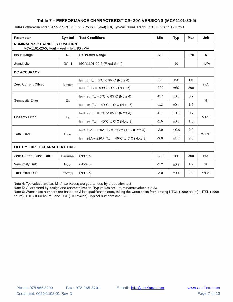
Table 7 – PERFORMANCE CHARACTERISTICS- 20A VERSIONS (MCA1101-20-5)
Unless otherwise noted: 4.5V < VCC < 5.5V, I(Vout) = I(Vref) = 0, Typical values are for VCC = 5V and TA = 25°C.
Parameter Symbol Test Conditions Min Typ Max Unit
NOMINAL Vout TRANSFER FUNCTION MCA1101-20-5, Vout = Vref + IIN x 90mV/A
Input Range IIN Calibrated Range -20 +20 A
Sensitivity GAIN MCA1101-20-5 (Fixed Gain) 90 mV/A
DC ACCURACY
Zero Current Offset IOFFSET
IIN = 0, TA = 0C to 85C (Note 4) -60 ±20 60
mA IIN = 0, TA = -40C to 0C (Note 5) -200 ±60 200
Sensitivity Error ES
IIN = IFS, TA = 0C to 85C (Note 4) -0.7 ±0.3 0.7
%
IIN = IFS, TA = -40C to 0C (Note 5) -1.2 ±0.4 1.2
Linearity Error EL
IIN = IFS, TA = 0C to 85C (Note 4) -0.7 ±0.3 0.7
%FS
IIN = IFS, TA = -40C to 0C (Note 5) -1.5 ±0.5 1.5
Total Error ETOT
IIN = ±6A ~ ±20A, TA = 0C to 85C (Note 4) -2.0 ± 0.6 2.0
% RD
IIN = ±6A ~ ±20A, TA = -40C to 0C (Note 5) -3.0 ±1.0 3.0
LIFETIME DRIFT CHARACTERISTICS
Zero Current Offset Drift IOFFSET(D) (Note 6) -300 60 300 mA
Sensitivity Drift ES(D) (Note 6) -1.2 0.3 1.2 %
Total Error Drift ETOT(D) (Note 6) -2.0 ±0.4 2.0 %FS
Note 4: Typ values are 1. Min/max values are guaranteed by production test
Note 5: Guaranteed by design and characterization. Typ values are 1, min/max values are 3. Note 6: Worst case numbers are based on 3 lots qualification data, taking the worst shifts from among HTOL (1000 hours), HTSL (1000
hours), THB (1000 hours), and TCT (700 cycles). Typical numbers are 1 .

CONFID ENTIAL
Phone: 978.965.3200 Fax: 978.965.3201 E-mail: [email protected] www.aceinna.com
Document: 6020-1102-01 Rev D Page 8 of 13
Table 8 – PERFORMANCE CHARACTERISTICS- 5A VERSIONS (MCA1101-5-5)
Unless otherwise noted: 4.5V < VCC < 5.5V, I(Vout) = I(Vref) = 0, Typical values are for VCC = 5V and TA = 25°C.
Parameter Symbol Test Conditions Min Typ Max Unit
NOMINAL Vout TRANSFER FUNCTION MCA1101-5-5, Vout = Vref + IIN x 350mV/A
Input Range IIN Calibrated Range -5 +5 A
Sensitivity GAIN MCA1101-5-5 (Fixed Gain) 350 mV/A
DC ACCURACY
Zero Current Offset IOFFSET
IIN = 0, TA = 0C to 85C (Note 4) -60 ±20 60
mA
IIN = 0, TA = -40C to 0C (Note 5) -60 ±20 60
Sensitivity Error ES
IIN = IFS, TA = 0C to 85C (Note 4) -1.0 ±0.4 1.0
%
IIN = IFS, TA = -40C to 0C (Note 5) -1.5 ±0.5 1.5
Linearity Error EL
IIN = IFS, TA = 0C to 85C (Note 4) -0.5 ±0.3 0.5
%FS
IIN = IFS, TA = -40C to 0C (Note 5) -0.75 ±0.4 0.75
Total Error ETOT
IIN = ±3A ~ ±5A, TA = 0C to 85C (Note 4) -2.0 ±1.0 2.0
% RD
IIN = ±3A ~ ±5A, TA = -40C to 0C (Note 5) -3.0 ±2.0 3.0
LIFETIME DRIFT CHARACTERISTICS
Zero Current Offset Drift IOFFSET(D) (Note 6) -300 70 300 mA
Sensitivity Drift ES(D) (Note 6) -1.3 0.3 1.3 %
Total Error Drift ETOT(D) (Note 6) -6 ±1.5 6 %FS
Note 4: Typ values are 1. Min/max values are guaranteed by production test
Note 5: Guaranteed by design and characterization. Typ values are 1, min/max values are 3. Note 6: Worst case numbers are based on 3 lots qualification data, taking the worst shifts from among HTOL (1000 hours), HTSL (1000
hours), THB (1000 hours), and TCT (700 cycles). Typical numbers are 1 .
CONFID ENTIAL
Phone: 978.965.3200 Fax: 978.965.3201 E-mail: [email protected] www.aceinna.com
Document: 6020-1102-01 Rev D Page 9 of 13
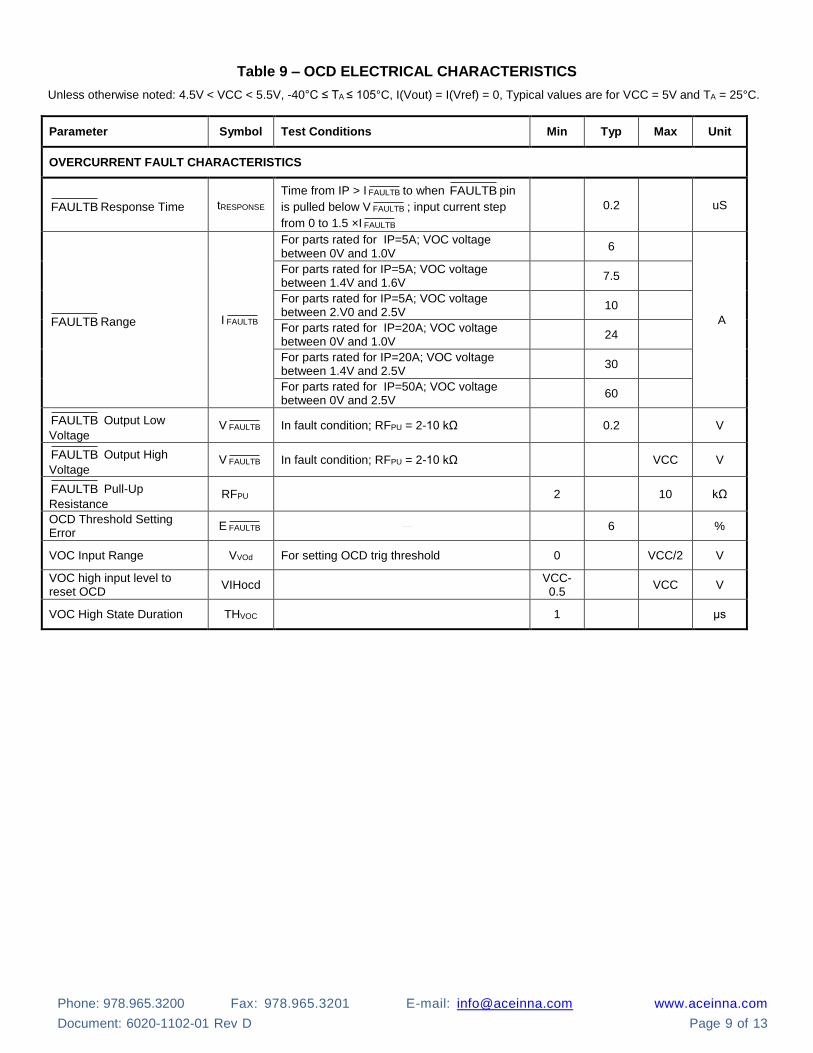
Table 9 – OCD ELECTRICAL CHARACTERISTICS
Unless otherwise noted: 4.5V < VCC < 5.5V, -40°C ≤ TA ≤ 105°C, I(Vout) = I(Vref) = 0, Typical values are for VCC = 5V and TA = 25°C.
Parameter Symbol Test Conditions Min Typ Max Unit
OVERCURRENT FAULT CHARACTERISTICS
FAULTB Response Time tRESPONSE
Time from IP > I FAULTB to when FAULTB pin
is pulled below V FAULTB ; input current step
from 0 to 1.5 ×I FAULTB
0.2 uS
FAULTB Range I FAULTB
For parts rated for IP=5A; VOC voltage between 0V and 1.0V
6
A
For parts rated for IP=5A; VOC voltage between 1.4V and 1.6V
7.5
For parts rated for IP=5A; VOC voltage between 2.V0 and 2.5V
10
For parts rated for IP=20A; VOC voltage between 0V and 1.0V
24
For parts rated for IP=20A; VOC voltage between 1.4V and 2.5V
30
For parts rated for IP=50A; VOC voltage between 0V and 2.5V
60
FAULTB Output Low
Voltage V FAULTB In fault condition; RFPU = 2-10 kΩ 0.2 V
FAULTB Output High
Voltage V FAULTB In fault condition; RFPU = 2-10 kΩ VCC V
FAULTB Pull-Up
Resistance RFPU 2 10 kΩ
OCD Threshold Setting Error
E FAULTB 6 %
VOC Input Range VVOd For setting OCD trig threshold 0 VCC/2 V
VOC high input level to reset OCD
VIHocd VCC-0.5
VCC V
VOC High State Duration THVOC 1 μs
CONFID ENTIAL
Phone: 978.965.3200 Fax: 978.965.3201 E-mail: [email protected] www.aceinna.com
Document: 6020-1102-01 Rev D Page 10 of 13
AMR TECHNOLOGY
Anisotropic magnetoresistance (AMR) makes use of a common material, Permalloy, to act as a magnetometer. Permalloy is an alloy containing roughly 80% nickel and 20% iron. The alloy’s resistance depends on the angle between the magnetization and the direction of current flow. In a magnetic field, magnetization rotates toward the direction of the magnetic field and the rotation angle depends on the external field’s magnitude. Permalloy’s resistance decreases as the direction of magnetization rotates away from the direction in which current flows, and is lowest when the magnetization is perpendicular to the direction of current flow. The resistance changes roughly as the square of the cosine of the angle between the magnetization and the direction of current flow. Permalloy is deposited on a silicon wafer and patterned as a resistive strip. The film’s properties cause it to change resistance in the presence of a magnetic field. In a current sensor application, two of these resistors are connected in a Wheatstone bridge configuration to permit the measurement of the magnitude of the magnetic field produced by the current.
AMR properties are well behaved when the film’s magnetic domains are aligned in the same direction. This configuration ensures high sensitivity, good repeatability, and minimal hysteresis. During fabrication, the film is deposited in a strong magnetic field that sets the preferred orientation, or “easy” axis, of the magnetization vector in the Permalloy resistors. AMR has better sensitivity than other methods and reasonably good temperature stability. The AMR sensor has sensitivity which is approximately a linear function of temperature.
FUNCTIONAL DESCRIPTION
Figure 2 provide block diagrams of the fixed gain. The AMR sensor monitors the magnetic field generated by the current flowing through the U shaped IP+/IP- package lead frame. The AMR sensor produces a voltage proportional to the magnetic field created by the positive or negative current in the IP+/IP- current loop while rejecting external magnetic interference. The sensor voltage is fed into a differential amplifier whose gain is temperature compensated. This is followed by an instrumentation amplifier output stage that provides a voltage that indicates the current passing through the IP+/IP- pins. To provide both positive and negative current data the Vout output pin is referenced to the Vref output pin. The voltage on the Vref output is typically one half of the full scale positive and negative range of the Vout current sense output signal. With no current flowing in the IP+/IP- pins, the voltage on the Vout output will typically equal the voltage on the Vref output. Positive IP+/IP- current causes the voltage on Vout to increase relative to Vref while negative IP+/IP- current will cause it to decrease.
GAIN
The sensor resistors are biased by an internal 4.35V reference voltage and the voltage on the Vref output is 2.175V (typical). This arrangement provides a fixed gain and enhanced supply rejection. The Vout pin drives to approximately 3.9V at full positive current and 0.3V at full negative current.
POWER UP / DOWN
An under-voltage lockout circuit monitors the voltage on the VCC pin. If the VCC voltage is less than the under-voltage threshold the MCA1101 is in an inactive state. Vout and Vref both drive to ground. If the VCC voltage exceeds the under-voltage threshold Vout and Vref are released and will drive to approximately half the VCC supply voltage and an initial calibration will commence. Once the initial calibration has completed the MCA1101 becomes active. Vout will slew to indicate the value of current flowing in the IP+/- conductor. Current flow in the IP+/- conductor with a VCC voltage less than the under-voltage threshold will not cause damage to the sensor.
OVERCURRENT DETECTION (OCD)
The MCA1101 have fast and accurate overcurrent fault
detection circuitry. The overcurrent fault threshold (I ) is
user-configurable via an external resistor divider and supports a range of 120% to 200% of the full-scale primary input (IP).
The overcurrent fault threshold (I ) is set via a resistor
divider from VCC to ground on the VOC pin. The voltage on the VOC pin (VVOC), may range from 0 ×VCC to 0.5 ×VCC. For +/-5A parts
For VVOC between 0 ×VCC and 0.225 ×VCC the I
threshold level is 1.2×IP.
For VVOC between 0.225 ×VCC and 0.35 ×VCC the I
threshold level is 1.5×IP.
For VVOC between 0.35 ×VCC and 0.5×VCC the I
threshold level is 2×IP. For +/-20A parts
For VVOC between 0 ×VCC and 0.225 ×VCC the I
threshold level is 1.2×IP.
For VVOC between 0.225 ×VCC and 0.5 ×VCC the I
threshold level is 1.5×IP. For +/-50A parts
For VVOC between 0 ×VCC and 0.5 ×VCC the I threshold
level is 1.2×IP.
If the input current exceeds the OCD threshold value I
the output pin will transition low and stay low, even
if input current drops below the threshold. In order to reset the
output the user needs to bring VOC pin to VCC and
hold it there for at least THvoc. . Once the OCD function is reset the VOC voltage should return back to its normal operating voltage Vvoc. A switch SW1 on Figure 1 can be used for this. Other methods are available as well. If OCD function is used, an OCD reset must be applied to the VOC pin after system power up, to put the OCD function and
pin in a known state.
The output is active low open drain. A pull-up
resistor should be connected between and VCC.
The VCC voltage will determine the high level of
signal. low output voltage is below 200mV.
The value of pull-up resistor is 2-10kOhm.
FAULTB
FAULTB
FAULTB
FAULTB
FAULTB
FAULTB
FAULTB
FAULTB
FAULTB
FAULTB
FAULTB
FAULTB
FAULTB
FAULTB
FAULTB FAULTB
CONFID ENTIAL
Phone: 978.965.3200 Fax: 978.965.3201 E-mail: [email protected] www.aceinna.com
Document: 6020-1102-01 Rev D Page 11 of 13
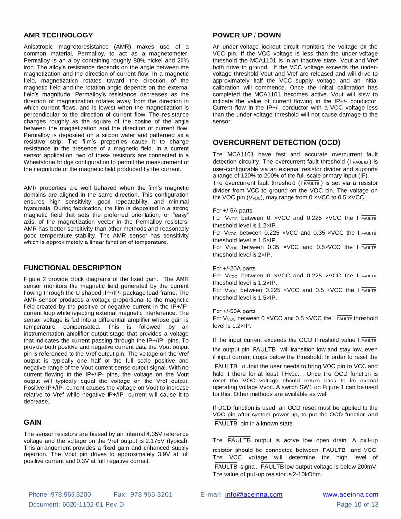
FREQUENCY RESPONSE
The MCA1101 offers a low noise and wideband response, with a 3dB bandwidth of > 1.5MHz, as shown in the plots below.
Figure 3 - Gain vs. Frequency
Figure 4 - Phase vs. Frequency
RESPONSE TIME
Vout response time is the time interval from 80% of the IP to 80% of the Vout. The response time is 300ns typical.
Figure 5 - Vout response time
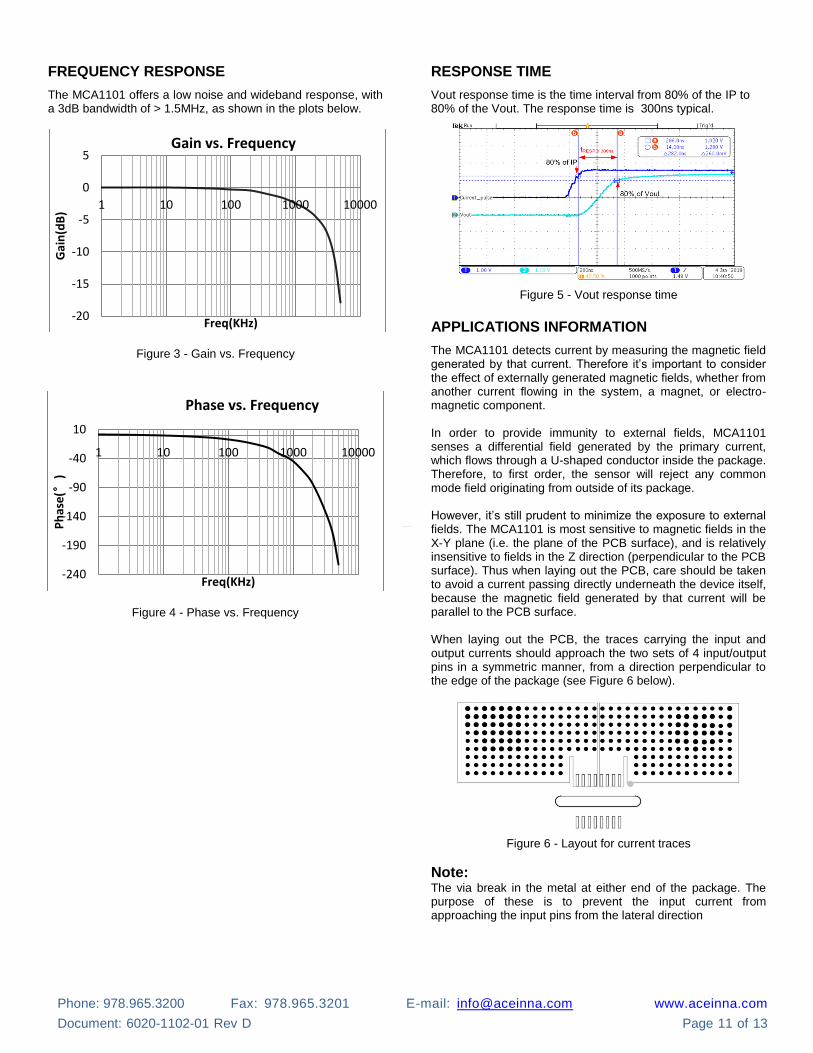
APPLICATIONS INFORMATION
The MCA1101 detects current by measuring the magnetic field generated by that current. Therefore it’s important to consider the effect of externally generated magnetic fields, whether from another current flowing in the system, a magnet, or electro-magnetic component. In order to provide immunity to external fields, MCA1101 senses a differential field generated by the primary current, which flows through a U-shaped conductor inside the package. Therefore, to first order, the sensor will reject any common mode field originating from outside of its package. However, it’s still prudent to minimize the exposure to external fields. The MCA1101 is most sensitive to magnetic fields in the X-Y plane (i.e. the plane of the PCB surface), and is relatively insensitive to fields in the Z direction (perpendicular to the PCB surface). Thus when laying out the PCB, care should be taken to avoid a current passing directly underneath the device itself, because the magnetic field generated by that current will be parallel to the PCB surface. When laying out the PCB, the traces carrying the input and output currents should approach the two sets of 4 input/output pins in a symmetric manner, from a direction perpendicular to the edge of the package (see Figure 6 below).
Figure 6 - Layout for current traces
Note: The via break in the metal at either end of the package. The purpose of these is to prevent the input current from approaching the input pins from the lateral direction
-20
-15
-10
-5
0
5
1 10 100 1000 10000
Gai
n(d
B)
Freq(KHz)
Gain vs. Frequency
-240
-190
-140
-90
-40
10
1 10 100 1000 10000
Ph
ase
(°)
Freq(KHz)
Phase vs. Frequency
CONFID ENTIAL
Phone: 978.965.3200 Fax: 978.965.3201 E-mail: [email protected] www.aceinna.com
Document: 6020-1102-01 Rev D Page 12 of 13
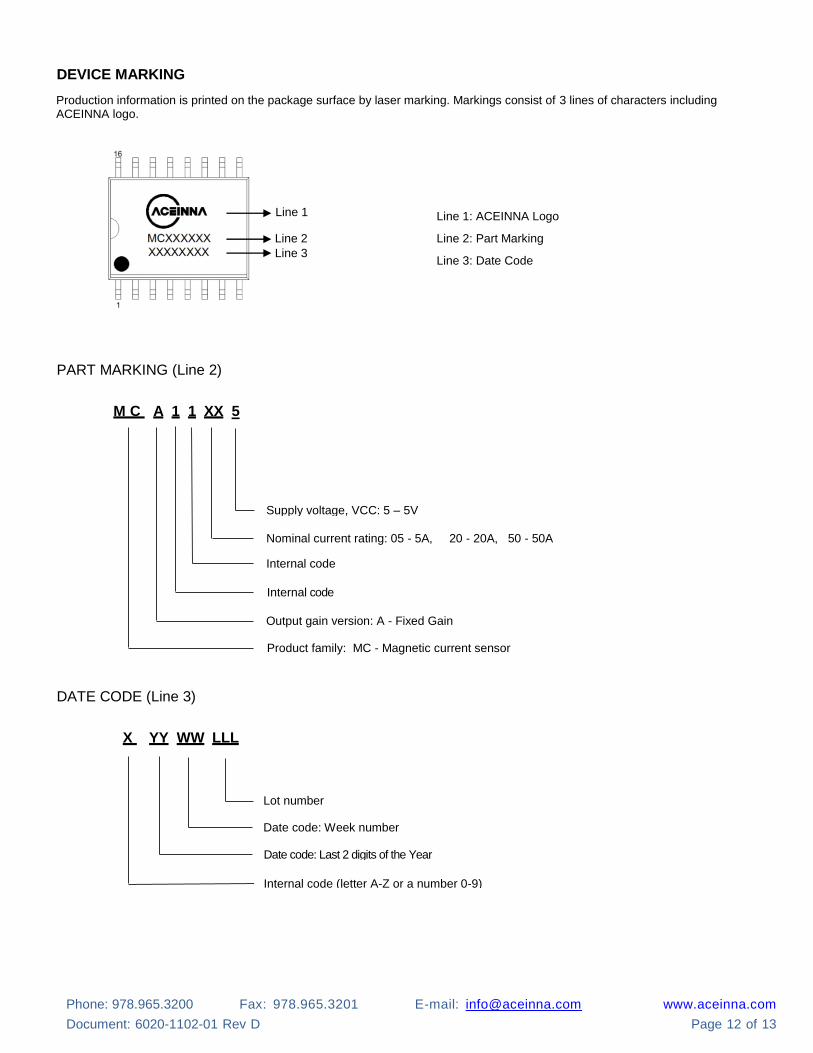
DEVICE MARKING
Line 1: ACEINNA Logo
Line 2: Part Marking
Line 3: Date Code
PART MARKING (Line 2)
M C A 1 1 XX 5
DATE CODE (Line 3)
X YY WW LLL
Line 1
Line 2
Line 3
Supply voltage, VCC: 5 – 5V
A Nominal current rating: 05 - 5A, 20 - 20A, 50 - 50A
Internal code
Internal code
Output gain version: A - Fixed Gain
Lot number
Date code: Week number
Date code: Last 2 digits of the Year
Internal code (letter A-Z or a number 0-9)
Product family: MC - Magnetic current sensor
Production information is printed on the package surface by laser marking. Markings consist of 3 lines of characters including ACEINNA logo.
CONFID ENTIAL
Phone: 978.965.3200 Fax: 978.965.3201 E-mail: [email protected] www.aceinna.com
Document: 6020-1102-01 Rev D Page 13 of 13
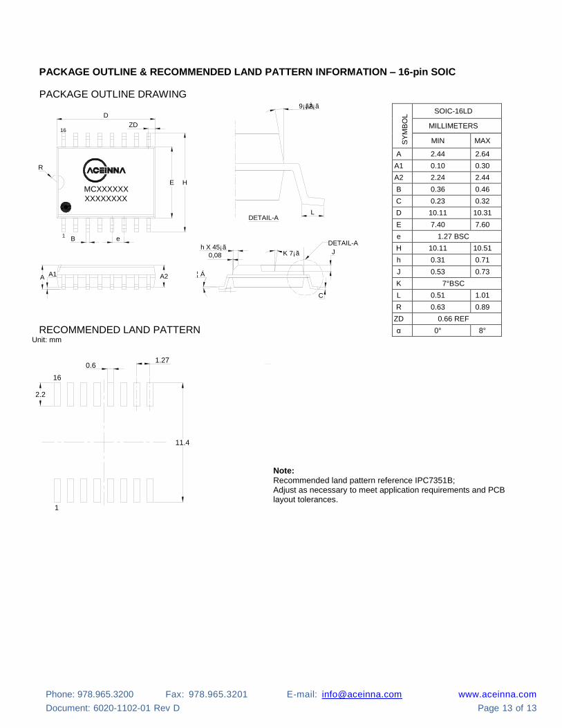
PACKAGE OUTLINE & RECOMMENDED LAND PATTERN INFORMATION – 16-pin SOIC
PACKAGE OUTLINE DRAWING
E H
B1
e
D
ZD
R
AA1 A2 ¦ Á
h X 45¡ã
C
J
DETAIL-A
DETAIL-AL
9¡ã¡ À2¡ã
16
K 7¡ã
MCXXXXXX
XXXXXXXX
0,08
RECOMMENDED LAND PATTERN
Unit: mm
11.4
0.61.27
2.2
1
16
SY
MB
OL SOIC-16LD
MILLIMETERS
MIN MAX
A 2.44 2.64
A1 0.10 0.30
A2 2.24 2.44
B 0.36 0.46
C 0.23 0.32
D 10.11 10.31
E 7.40 7.60
e 1.27 BSC
H 10.11 10.51
h 0.31 0.71
J 0.53 0.73
K 7°BSC
L 0.51 1.01
R 0.63 0.89
ZD 0.66 REF
α 0° 8°
Note:
Recommended land pattern reference IPC7351B; Adjust as necessary to meet application requirements and PCB layout tolerances.