Magazine summer98 p18
2
Summer 1998 Yield Management Solutions 18 Reduce Lithography Tool Qualification Time with High-Throughput CD SEMs by Richard Elliott, Strategic Marketing Manager best focus at any position is determined by measuring features printed through the range of useable focus, then plotting the CDs vs. focus value. 25 focus steps usually provide a clean curve to determine the point of best focus repeatably. To identify any performance variation due to feature type or orientation, multiple features are often measured at each site. Typical features used are isolated and dense lines in the horizontal and vertical direction, which yields four measurements at each site. Sagital and tangential orientations can be added, but this doubles the number of measurements required. With 4 measurements per site at 25 focus steps, 100 measurements are required per position in the exposure field. To compare the focal plane position between 9 points in a single field, 900 measurements are required. This volume of measurement seems immense, but fast automated move-acquire-measure (MAM) times can bring this experiment down to a manageable time. With a six second MAM time, this experiment takes about an hour and a half for one wafer. Automatic macros for analysis make this practical to do. Tests which might take hours longer on slower CD SEMs, or even days on manual metrology tools, can now be completed quickly. Fast MAM time opens the door for larger, more exten- sive experiments. Recent improvements in productivity parallel funda- mental advancements made in CD SEM electron optics and metrology. State-of-the-art systems are capable of 3 nm measurement precision and imaging of features with aspect ratios as high as 10:1. Coupled with this advanced metrology capability, fast MAM time enables more extensive characterization in less time and ensures that metrology tools can support lithography tool char- acterization as process parameters increase. Process characterization and optimization become increasingly difficult as minimum dimensions are reduced. CD tolerance limits must tighten to meet the requirements of smaller design rules and advanced device designs. The lithography process advances made to achieve these smaller CDs add new variables to the lithography equation. Advances include: • the use of different photoresists for line/space layers and contact layers, • the availability of variable illumination partial coher- ence (σ) and numerical aperture (NA) lithography systems which require optimization, and • production use of Optical Proximity Correction (OPC) and Phase-Shift Masks (PSM). In addition, the introduction of step and scan technolo- gy creates new requirements for equipment stability monitoring. For steppers, the CD variation across the exposure field is generally stable. For step and scan systems, reticle and wafer motion during exposure can vary over time. This “rubber lens” effect produces a new source of across chip linewidth variation (ACLV) which must be monitored periodically. Fast measurement speeds characterization Consider a typical lens characterization designed to determine the focal plane deviation across a stepper field. Metrics of interest include the total range of focal plane variation across the field and the identification of the two points between which the largest variation is seen. To determine these values, focus curves from multiple points within the field are generated and compared. The Metrology F EATURES Lithography tool and process characterization are at the core of lithography process engineer- ing. Critical Dimension (CD) measurement and CD uniformity performance are primary ele- ments used in the selection of equipment and process parameters. Bosung plots, swing curves, E-D trees and other forms of CD data analysis are familiar icons to lithography engineers. Assessment of system performance requires very large amounts of data, and the time required to collect this data can impede a thorough characterization experiment.
-
Upload
kla-tencor -
Category
Documents
-
view
219 -
download
1
description
Â
Transcript of Magazine summer98 p18
MetrologyF E A T U R E S
Reduce Lithography Tool QualificationTime with High-Throughput CD SEMs
by Richard Elliott, Strategic Marketing Manager
Lithography tool and process characterization are at the core of lithography process engineer-ing. Critical Dimension (CD) measurement and CD uniformity performance are primary ele-ments used in the selection of equipment and process parameters. Bosung plots, swing curves,E-D trees and other forms of CD data analysis are familiar icons to lithography engineers.Assessment of system performance requires very large amounts of data, and the time requiredto collect this data can impede a thorough characterization experiment.
Process characterization and optimization becomeincreasingly difficult as minimum dimensions arereduced. CD tolerance limits must tighten to meet the requirements of smaller design rules and advanceddevice designs. The lithography process advances madeto achieve these smaller CDs add new variables to thelithography equation. Advances include:
• the use of different photoresists for line/space layersand contact layers,
• the availability of variable illumination partial coher-ence (σ) and numerical aperture (NA) lithographysystems which require optimization, and
• production use of Optical Proximity Correction(OPC) and Phase-Shift Masks (PSM).
In addition, the introduction of step and scan technolo-gy creates new requirements for equipment stabilitymonitoring. For steppers, the CD variation across theexposure field is generally stable. For step and scan systems, reticle and wafer motion during exposure canvary over time. This “rubber lens” effect produces a newsource of across chip linewidth variation (ACLV) whichmust be monitored periodically.
Fast measurement speeds characterizationConsider a typical lens characterization designed todetermine the focal plane deviation across a stepper field.Metrics of interest include the total range of focal planevariation across the field and the identification of the twopoints between which the largest variation is seen. Todetermine these values, focus curves from multiplepoints within the field are generated and compared. The
Summer 1998 Yield Management Solutions18
best focus at any position is determined by measuringfeatures printed through the range of useable focus, thenplotting the CDs vs. focus value. 25 focus steps usuallyprovide a clean curve to determine the point of bestfocus repeatably. To identify any performance variationdue to feature type or orientation, multiple features areoften measured at each site. Typical features used are isolated and dense lines in the horizontal and verticaldirection, which yields four measurements at each site.Sagital and tangential orientations can be added, butthis doubles the number of measurements required.With 4 measurements per site at 25 focus steps, 100measurements are required per position in the exposurefield. To compare the focal plane position between 9points in a single field, 900 measurements are required.
This volume of measurement seems immense, but fastautomated move-acquire-measure (MAM) times canbring this experiment down to a manageable time. Witha six second MAM time, this experiment takes about anhour and a half for one wafer. Automatic macros foranalysis make this practical to do. Tests which mighttake hours longer on slower CD SEMs, or even days onmanual metrology tools, can now be completed quickly.Fast MAM time opens the door for larger, more exten-sive experiments.
Recent improvements in productivity parallel funda-mental advancements made in CD SEM electron opticsand metrology. State-of-the-art systems are capable of 3 nm measurement precision and imaging of featureswith aspect ratios as high as 10:1. Coupled with thisadvanced metrology capability, fast MAM time enablesmore extensive characterization in less time and ensuresthat metrology tools can support lithography tool char-acterization as process parameters increase.
Productivity features parallel increasing metrology requirementsFast MAM time is not the only pro-ductivity capability needed to meetincreasing metrology requirements.The development of the followingproductivity features on advancedCD SEMs has paralleled the devel-opment of the lithography tools:
• High throughput enables mas-sive measurement data collec-tion.
• Full automation and the subse-quent removal of human errorsin the association of measure-ment data to experimental condi-tions improves data integrity.
• Library-based recipe program-ming allows for the reuse ofinformation pertaining to com-mon structures and enables thewaferless creation of recipes off-line.
The new OMNIMAP® RS-100 delivers thehave been asking for.
• Accurate e
The First Producti300 mm ResistivityMeasurement Syste
• Data files with all relevant mea-surement conditions and that canassociate specific measurementlocations directly with exact con-ditions such as focus and expo-sure enable simpler data analysis.
• Improved user interfaces enabledirect labeling of image artifactsfor documentation and reporting.
features customers
dge measurement to 1 mm from the conductive film
• Powerful and easy to use Windows NT® platform
• Full GEM/SECS HSMScompatibility and more
• Expanded sensitivity for highly conductive interconnects such as
copper and thick aluminum• Automated probe conditioner
• 3D uniformity maps• 200 mm and 300 mm config• Meets SEMI safety and ergo
on-Ready
m
Visit our website at www.kla-teFor more information call 800
• Advanced measurement algo-rithms provide data such as leftvs. right line edge comparison,line edge roughness, cornerrounding, or contact area infor-mation.
These productivity features availableon tools such as the KLA-Tencor8100XP can combine to make characterization a simple turnkeyoperation.
circle RS#009
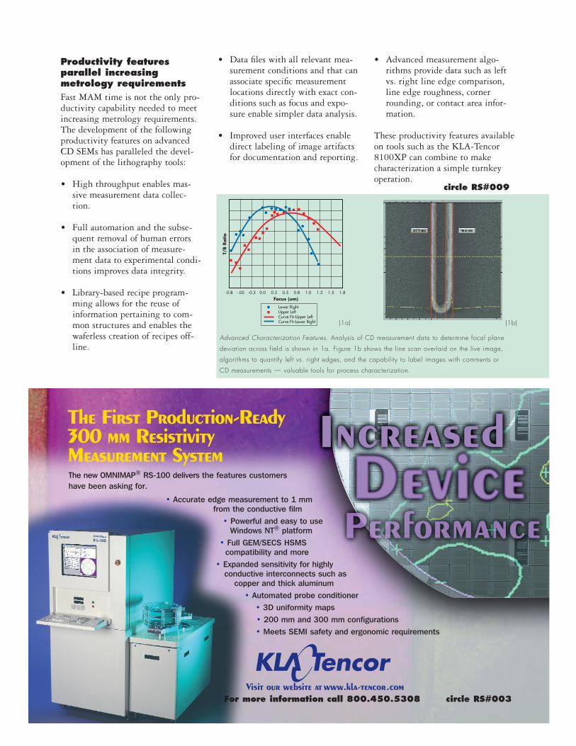
Advanced Characterization Features. Analysis of CD measurement data to determine focal plane
deviation across field is shown in 1a. Figure 1b shows the line scan overlaid on the live image,
algorithms to quantify left vs. right edges, and the capability to label images with comments or
CD measurements — valuable tools for process characterization.
-0.8 -.05 -0.3 0.0 0.3 0.5 0.8 1.0 1.3 1.5 1.8
T/B R
atio
Focus (um)
Lower RightUpper LeftCurve Fit-Upper LeftCurve Fit-Lower Right (1a) (1b)
urationsnomic requirements
ncor.com.450.5308 circle RS#003