LTC3646/LTC3646-1 - 40V, 1A Synchronouscds.linear.com/docs/en/datasheet/36461fc.pdf ·...
28
LTC3646/LTC3646-1 1 36461fc For more information www.linear.com/LTC3646 TYPICAL APPLICATION FEATURES DESCRIPTION 40V, 1A Synchronous Step-Down Converter The LTC ® 3646 is a high efficiency, step-down DC/DC converter with internal high side and synchronous power FETs. It draws only 140µA typical DC supply current in Burst Mode operation at no load while maintaining output voltage regulation. The LTC3646 can supply up to a 1A load, and its combina- tion of Burst Mode operation, integrated power switches and low quiescent current provides high efficiency over a broad range of load currents. Alternatively, it can be used in forced continuous mode for ripple sensitive applications. The LTC3646 has a wide 4.0V to 40V input range and its patented controlled on-time architecture and 0.6V refer- ence voltage allow for large step-down ratios without the risk of output overvoltage. The frequency may be set between 200kHz and 3.0MHz with a program resistor or synchronized to an external clock. The internal soft-start, short-circuit protection and volt- age rating make the LTC3646 a robust part ideal for high voltage applications. Efficiency Curve APPLICATIONS n Wide Input Voltage Range: 4.0V to 40V n 1A Guaranteed Output Current n High Efficiency: Up to 95% n Wide Output Voltage Range n LTC3646: 2.0V to 30V n LTC3646-1: 0.6V to 15V n ±1% Accurate Reference Voltage n Internal or External Compensation n Switching Frequency Adjustable and Synchronizable: 200kHz to 3MHz n Selectable High Efficiency Burst Mode ® Operation or Forced Continuous Mode n 14 Lead 3mm × 4mm DFN or Thermally Enhanced 16-Lead MSOP Packages n Point of Load Power Supplies n Intermediate Bus Power n Automotive Applications L, LT, LTC, LTM, Linear Technology, the Linear logo and Burst Mode are registered trademarks and Hot Swap is a trademark of Linear Technology Corporation. All other trademarks are the property of their respective owners. Protected by U.S. Patents, including 6580258, 5481178, 5994885, 6304066, 5847554, 6476589, 6774611. LOAD CURRENT (A) 0.001 EFFICIENCY (%) POWER LOSS (W) 40 60 1 3646 TA01b 20 0 0.1 0.01 100 30 50 10 70 80 90 0.4 0.2 0.8 0 1.0 0.6 V OUT = 3.3V V OUT = 5V V OUT = 3.3V V OUT = 5V V IN = 12V f = 1MHz PVIN SVIN RUN INTV CC MODE/SYNC ITH RT EXTV CC BOOST SW V ON V FB + – SWITCH CONTROL LTC3646 3.3μH SGND 4.7μF PGND 0.1μF 412k 10μF 0.6V 56.2k 3646 TA01a 15μF V OUT 5V 1A V IN 40V MAX
Transcript of LTC3646/LTC3646-1 - 40V, 1A Synchronouscds.linear.com/docs/en/datasheet/36461fc.pdf ·...
LTC3646/LTC3646-1
136461fc
For more information www.linear.com/LTC3646
TYPICAL APPLICATION
FEATURES DESCRIPTION
40V, 1A Synchronous Step-Down Converter
The LTC®3646 is a high efficiency, step-down DC/DC converter with internal high side and synchronous power FETs. It draws only 140µA typical DC supply current in Burst Mode operation at no load while maintaining output voltage regulation.
The LTC3646 can supply up to a 1A load, and its combina-tion of Burst Mode operation, integrated power switches and low quiescent current provides high efficiency over a broad range of load currents. Alternatively, it can be used in forced continuous mode for ripple sensitive applications.
The LTC3646 has a wide 4.0V to 40V input range and its patented controlled on-time architecture and 0.6V refer-ence voltage allow for large step-down ratios without the risk of output overvoltage. The frequency may be set between 200kHz and 3.0MHz with a program resistor or synchronized to an external clock.
The internal soft-start, short-circuit protection and volt-age rating make the LTC3646 a robust part ideal for high voltage applications.
Efficiency Curve
APPLICATIONS
n Wide Input Voltage Range: 4.0V to 40V n 1A Guaranteed Output Current n High Efficiency: Up to 95% n Wide Output Voltage Range
n LTC3646: 2.0V to 30V n LTC3646-1: 0.6V to 15V
n ±1% Accurate Reference Voltage n Internal or External Compensation n Switching Frequency Adjustable and Synchronizable:
200kHz to 3MHz n Selectable High Efficiency Burst Mode® Operation or
Forced Continuous Mode n 14 Lead 3mm × 4mm DFN or Thermally Enhanced
16-Lead MSOP Packages
n Point of Load Power Supplies n Intermediate Bus Power n Automotive Applications
L, LT, LTC, LTM, Linear Technology, the Linear logo and Burst Mode are registered trademarks and Hot Swap is a trademark of Linear Technology Corporation. All other trademarks are the property of their respective owners. Protected by U.S. Patents, including 6580258, 5481178, 5994885, 6304066, 5847554, 6476589, 6774611.
LOAD CURRENT (A)0.001
EFFI
CIEN
CY (%
)
POWER LOSS (W
)
40
60
1
3646 TA01b
20
00.10.01
100
30
50
10
70
80
90
0.4
0.2
0.8
0
1.0
0.6
VOUT = 3.3V
VOUT = 5V
VOUT = 3.3V
VOUT = 5VVIN = 12Vf = 1MHz
PVIN
SVIN
RUN
INTVCC
MODE/SYNC
ITH
RT
EXTVCC
BOOST
SW
VON
VFB+ –
SWITCHCONTROL
LTC36463.3µH
SGND
4.7µF
PGND
0.1µF
412k
10µF
0.6V
56.2k
3646 TA01a
15µF
VOUT5V1A
VIN40V MAX

LTC3646/LTC3646-1
236461fc
For more information www.linear.com/LTC3646
ABSOLUTE MAXIMUM RATINGSPVIN, SVIN Supply Voltage ........................ –0.3V to 45VSW Voltage (DC) ........................... –0.3V to PVIN + 0.3VBOOST – SW Voltage ................................... –0.3V to 6VVON Voltage ................................................ –0.3V to 33VMODE/SYNC, RT, ITH, VFB Voltage ................................–0.3V to INTVCC + 0.3VINTVCC Voltage ............................................ –0.3V to 6V
(Notes 1, 7)
1
2
3
4
5
6
7
14
13
12
11
10
9
8
SVIN
RUN
EXTVCC
INTVCC
BOOST
SW
PVIN
SGND
VFB
ITH
RT
VON
PGOOD
MODE/SYNC
TOP VIEW
15PGND
DE PACKAGE14-LEAD (4mm × 3mm) PLASTIC DFN
TJMAX = 150°C, θJA = 43°C/W EXPOSED PAD (PIN 15) IS PGND, MUST BE SOLDERED TO PCB
12345678
SGNDVFBITHRT
VONPGOOD
MODE/SYNCNC
161514131211109
SVINRUNEXTVCCINTVCCBOOSTSWPVINPVIN
TOP VIEW
17PGND
MSE PACKAGE16-LEAD PLASTIC MSOP
TJMAX = 150°C, θJA = 38°C/W EXPOSED PAD (PIN 17) IS PGND, MUST BE SOLDERED TO PCB
PIN CONFIGURATION
ORDER INFORMATIONLEAD FREE FINISH TAPE AND REEL PART MARKING PACKAGE DESCRIPTION TEMPERATURE RANGE
LTC3646EDE#PBF LTC3646EDE#TRPBF 3646 14-Lead (4mm × 3mm) Plastic DFN –40°C to 85°C
LTC3646IDE#PBF LTC3646IDE#TRPBF 3646 14-Lead (4mm × 3mm) Plastic DFN –40°C to 125°C
LTC3646HDE#PBF LTC3646HDE#TRPBF 3646 14-Lead (4mm × 3mm) Plastic DFN –40°C to 150°C
LTC3646EMSE#PBF LTC3646EMSE#TRPBF 3646 16-Lead Plastic MSOP –40°C to 85°C
LTC3646IMSE#PBF LTC3646IMSE#TRPBF 3646 16-Lead Plastic MSOP –40°C to 125°C
LTC3646HMSE#PBF LTC3646HMSE#TRPBF 3646 16-Lead Plastic MSOP –40°C to 150°C
LTC3646EDE-1#PBF LTC3646EDE-1#TRPBF 36461 14-Lead (4mm × 3mm) Plastic DFN –40°C to 85°C
LTC3646IDE-1#PBF LTC3646IDE-1#TRPBF 36461 14-Lead (4mm × 3mm) Plastic DFN –40°C to 125°C
LTC3646HDE-1#PBF LTC3646HDE-1#TRPBF 36461 14-Lead (4mm × 3mm) Plastic DFN –40°C to 150°C
LTC3646EMSE-1#PBF LTC3646EMSE-1#TRPBF 36461 16-Lead Plastic MSOP –40°C to 85°C
LTC3646IMSE-1#PBF LTC3646IMSE-1#TRPBF 36461 16-Lead Plastic MSOP –40°C to 125°C
LTC3646HMSE-1#PBF LTC3646HMSE-1#TRPBF 36461 16-Lead Plastic MSOP –40°C to 150°C
Consult LTC Marketing for parts specified with wider operating temperature ranges. *The temperature grade is identified by a label on the shipping container.For more information on lead free part marking, go to: http://www.linear.com/leadfree/ For more information on tape and reel specifications, go to: http://www.linear.com/tapeandreel/
EXTVCC Voltage ........................................... –0.3V to 6VRUN Voltage............................................... –0.3V to 45VPGOOD .......................................–0.3V to INTVCC + 0.3VOperating Junction Temperature Range(Notes 2, 7) ............................................ –40°C to 150°CStorage Temperature Range .................. –65°C to 150°CLead Temperature (Soldering, 10 sec) MSE .......... 300°C
LTC3646/LTC3646-1
336461fc
For more information www.linear.com/LTC3646
ELECTRICAL CHARACTERISTICS The l denotes the specifications which apply over the specified operating junction temperature range, otherwise specifications are at TA = 25°C (Note 2), PVIN = SVIN = 12V unless otherwise noted.
SYMBOL PARAMETER CONDITIONS MIN TYP MAX UNITSInput Supply (PVIN, SVIN)VIN Input Voltage Operating Range l 4.0 40 VVIN(OV) Input Supply Overvoltage Lockout VIN Rising
Hysteresis (VIN Falling)l
l
43.5 2.0
46 2.5
2.9
V V
VIN(UV) Input Supply Undervoltage Lockout VIN Falling Hysteresis (VIN Rising)
3.2 3.35 250
3.5 V mV
IQ DC Supply Current (Note 3) Forced Continuous Sleep Mode Shutdown Mode
VRUN = 0V
620 140 8
875 190
µA µA µA
Main Control LoopVOUT Output Voltage Range (Note 4) LTC3646
LTC3646-12.0 0.6
30 15
V V
VFB Feedback Reference Voltage –40°C < TA < 85°C
l
0.594 0.591
0.6 0.6
0.606 0.609
V V
Feedback Voltage Line Regulation VIN = 4.0V to 40V, ITH = 1.5V 0.05 %/VFeedback Voltage Load Regulation ITH = 1.0V to 1.8V 0.12 %Feedback Input Current VFB = 0.6V l 0 ±20 nA
gm(EA) Error Amplifier Transconductance External Comp 300 µStON(MIN) Minimum On-Time VIN = 40V, RRT = 30k, VON = 2V 30 nstOFF(MIN) Minimum Off-Time 80 nsILIM Valley Switch Current Limit l 0.9 1.2 1.5 A
Negative Valley Switch Current Limit –0.3 AInternal Oscillator Frequency VRT = VINTVCC
RRT = 450kΩ RRT = 60kΩ RRT = 30kΩ
1.6 0.19 1.25 2.55
2.25 0.2 1.5 3.0
2.95 0.27 1.75 3.45
MHz MHz MHz MHz
External Clock Frequency Range 0.2 3.0 MHzRDS(ON) Top Switch On-Resistance (Note 5)
Bottom Switch On-Resistance (Note 5)VIN = 5.5V VIN = 5.5V
200 120
mΩ mΩ
Switch Leakage VIN = VSW = 40V, VRUN = 0V VIN = 40V, VSW = 0V, VRUN = 0V
±1 ±1
µA µA
Internal VCC RegulatorVINTVCC INTVCC Voltage IINTVCC = 5mA l 4.8 5.0 5.2 V
INTVCC Load Regulation (Note 6) IINTVCC = 0mA to 5mA 0.5 %INTVCC Undervoltage Lockout INTVCC Falling 3.0 VINTVCC UVLO Hysteresis 0.3 VEXTVCC Switchover Voltage EXTVCC Rising 4.25 4.5 4.65 VEXTVCC Hysteresis 200 mV
OperationVRUN RUN Pin Threshold RUN Rising
RUN Falling Hysteresis
1.17 1.06
1.21 1.10 110
1.26 1.14
V V
mVRUN Pin Leakage Current RUN = 1.3V 0 ±1 µA
VPGOOD(UT) PGOOD Overvoltage Threshold FB Rising FB Falling
5.0 3.5
7.5 5
10 %VFB %VFB
VPGOOD(LT) PGOOD Undervoltage Threshold FB Falling FB Rising
–5.0 –3.5
–7.5 –5
–10 %VFB %VFB

LTC3646/LTC3646-1
436461fc
For more information www.linear.com/LTC3646
ELECTRICAL CHARACTERISTICS The l denotes the specifications which apply over the specified operating junction temperature range, otherwise specifications are at TA = 25°C (Note 2), PVIN = SVIN = 12V unless otherwise noted.
SYMBOL PARAMETER CONDITIONS MIN TYP MAX UNITStPGOOD PGOOD Filter Time RT = INTVCC 15 30 µsRPGOOD PGOOD Pull-Down Resistance IPGOOD = 10mA 63 Ω
PGOOD Leakage VPGOOD = VINTVCC 1.0 µAtSS Internal Soft-Start Time 250 500 µsVMODE/SYNC Mode Threshold Voltage
SYNC Threshold Voltage
Mode VIH Mode VIL SYNCIH SYNCIL
l
l
l
l
1.2
1.2
0.3
0.3
V V V V
MODE/SYNC Input Current 1 2 µAInternal ITH Voltage Threshold l INTVCC – 0.3V VVON Pin Input Impedance LTC3646
LTC3646-1520 600
kΩ kΩ
Note 1: Stresses beyond those listed under Absolute Maximum Ratings may cause permanent damage to the device. Exposure to any Absolute Maximum Rating condition for extended periods may affect device reliability and lifetime.Note 2: The LTC3646 is tested under pulsed load conditions such that TJ ≈ TA. The LTC3646E is guaranteed to meet specifications from 0°C to 85°C junction temperature. Specifications over the –40°C to 125°C operating junction temperature range are assured by design, characterization and correlation with statistical process controls. The LTC3646I is guaranteed over the –40°C to 125°C operating junction temperature range and the LTC3646H is guaranteed over the –40°C to 150°C operating junction temperature range. High junction temperatures derate operating lifetimes; operating lifetime is derated for junction temperatures greater than 125°C. Note that the maximum ambient temperature consistent with these specifications is determined by specific operating conditions in conjunction with board layout, the rated package thermal impedance and other environmental factors.
Note 3: Dynamic supply current is higher due to gate charging being delivered at the switch frequency. Note 4: Limits to VOUT are a subject to PVIN, SVIN, tON(MIN), tOFF(MIN), and frequency constraints. See the Applications Information section for a further discussion. These items are tested with appropriate combinations of VIN, VON and frequency.Note 5: RDS(ON) is guaranteed by correlation to wafer level measurements.Note 6: Maximum allowed current draw when used as a regulated output is 5mA. This supply is only intended to provide additional DC load current as needed and not to regulate large transient or AC behavior as such waveforms may impact LTC3646 operation.Note 7: This IC includes overtemperature protection intended to protect the device during momentary overload conditions. The maximum junction temperature may be exceeded when overtemperature protection is active. Continuous operation above the specified maximum operating junction temperature may result in device degradation or failure.
LTC3646/LTC3646-1
536461fc
For more information www.linear.com/LTC3646
TYPICAL PERFORMANCE CHARACTERISTICS
Efficiency vs Input Voltage, Burst Mode Operation
Reference Voltage vs Temperature RDS(ON) vs Temperature
Switch Pin Leakage vs Temperature and Supply
Oscillator Internal Set Frequency vs Temperature
Efficiency vs Load Current, Burst Mode Operation
Efficiency vs Load Current, Forced Continuous Mode Operation Efficiency vs Load Current
TA = 25°C, SVIN/PVIN = 12V, fO = 1MHz unless otherwise noted.
Oscillator Externally Set Frequency vs Temperature
INPUT VOLTAGE (V)0
EFFI
CIEN
CY (%
)
80
90
40
36461 G04
70
60105
100
75
85
65
95
15 20 25 30 35
LOAD = 500mA
LOAD = 100mA
LOAD = 1A
L = 6.8µHVOUT = 3.3V
TEMPERATURE (°C)–50
RESI
STAN
CE (Ω
)0.20
0.30
150130110
36461 G06
0.10
0–10–30
0.35
0.15
0.25
0.05
10 30 50 70 90
MAIN SWITCH
SYNCHRONOUS SWITCH
TEMPERATURE (°C)–50
SW L
EAKA
GE C
URRE
NT (µ
A)
14
18
150130110
36461 G07
10
0–10–30
20
12
16
8
4
6
2
10 30 50 70 90
VDS = 12V, MAIN SWITCHVDS = 12V, SYNCHRONOUS SWITCHVDS = 40V, MAIN SWITCHVDS = 40V, SYNCHRONOUS SWITCH
TEMPERATURE (°C)–40
FREQ
UENC
Y (M
Hz) 2.35
2.45
140120100
36461 G08
2.25
2.000–20
2.50
2.30
2.40
2.20
2.10
2.15
2.05
20 40 60 80
VRT = VINTVCC
TEMPERATURE (°C)–40
FREQ
UENC
Y (M
Hz)
1.5
1.7
140120100
36461 G09
1.3
1.20–20
1.8
1.4
1.6
20 40 60 80
RRT = 60k
TEMPERATURE (°C)–50
V REF
(mV)
600
604
150130110
36461 G05
596
592–10–30
608
598
602
594
606
10 30 50 70 90
LOAD CURRENT (A)0.001
EFFI
CIEN
CY (%
)
40
60
1
36461 G01
20
00.10.01
100
30
50
10
70
80
90
VIN = 5VVIN = 8VVIN = 12V
VOUT = 1.8VfO = 1.5MHz
LOAD CURRENT (A)0.001
EFFI
CIEN
CY (%
)40
60
1
36461 G02
20
00.10.01
100
30
50
10
70
80
90
VIN = 5VVIN = 8VVIN = 12V
VOUT = 1.8VfO = 1.5MHz
LOAD CURRENT (A)0.001
EFFI
CIEN
CY (%
)
40
60
1
36461 G03
20
00.10.01
100
30
50
10
70
80
90
FORCED CONTINUOUSOPERATION
VOUT = 5VVOUT = 3.3V
Burst Mode OPERATION

LTC3646/LTC3646-1
636461fc
For more information www.linear.com/LTC3646
TYPICAL PERFORMANCE CHARACTERISTICS
Output Voltage vs Time, Burst Mode Operation
Start-Up from Shutdown, Burst Mode Operation
Start-Up from Shutdown, Forced Continuous Mode
Load Step, Burst Mode OperationLoad Step, Forced Continuous Operation
IQ Shutdown vs Supply and Temperature
TA = 25°C, SVIN/PVIN = 12V, fO = 1MHz unless otherwise noted.
Bottom Switch Current Limit vs Temperature
No Load Quiescent Current vs Temperature, Burst Mode Operation Load Regulation
TEMPERATURE (°C)–40
NO L
OAD
QUIE
SCEN
T CU
RREN
T (µ
A)
140
180
140120100
36461 G10
1000–20
200
120
160
20 40 60 80TEMPERATURE (°C)
–40
BOTT
OM S
WIT
CH C
URRE
NT L
IMIT
(A)
1.2
1.4
140120100
36461 G11
1.00–20
1.5
1.1
1.3
20 40 60 80LOAD CURRENT (A)
0
∆VOU
T/V O
UT (%
)
0.8 1
36461 G12
–0.40.2 0.4 0.6
1.6
0
0.4
0.8
1.2
VOUT = 5V
FORCED CONTINUOUSBurst Mode OPERATION
VIN = 12VVOUT = 5VILOAD = 20mA
2µs/DIV 36461 G13
VOUT20mV/DIV
AC-COUPLED
IL250mA/DIV
SW10V/DIV
ILOAD = 25mA 100µs/DIV 36461 G14
VOUT5V/DIV
IL250mA/DIV
RUN5V/DIV
ILOAD = 25mA 100µs/DIV 36461 G15
VOUT5V/DIV
IL250mA/DIV
RUN5V/DIV
VOUT = 1.2V50mA to 1A STEPfO = 2.25MHzRCOMP = 200kΩCCOMP = 33pFCF = 10pFCOUT = 15µF
40µs/DIV 36461 G16
VOUTAC-COUPLED
100mV/DIV
IL1A/DIV
ILOAD1A/DIV
VOUT = 1.2V50mA to 1A STEPfO = 2.25MHzRCOMP = 200kΩCCOMP = 33pFCF = 10pFCOUT = 15µF
10µs/DIV 36461 G17
VOUTAC-COUPLED
100mV/DIV
IL1A/DIV
ILOAD1A/DIV
TEMPERATURE (°C)–40
SHUT
DOW
N CU
RREN
T (µ
A)
80 120 140100
36461 G18
0–20 200 40 60
60
10
20
30
40
50
VIN = 40VVIN = 12V

LTC3646/LTC3646-1
736461fc
For more information www.linear.com/LTC3646
PIN FUNCTIONS (DFN/MSOP)
SGND (Pin 1/Pin 1): Analog Ground Pin. This pin should have a low noise connection to the reference ground.
VFB (Pin 2/Pin 2): Output Voltage Feedback Pin. Input to the error amplifier that compares the feedback voltage with the internal 0.6V reference. Connect this pin to a resistor divider network to program the desired output voltage.
ITH (Pin 3/Pin 3): Error Amplifier Output and Switching Regulator Compensation Point. Connect this pin to appro-priate external components to compensate the regulator loop frequency response. Connect this pin to INTVCC to use the default internal compensation.
RT (Pin 4/Pin 4): Oscillator Frequency Program Pin. Con-nect an external resistor between 450k and 30k from this pin to SGND to program the switching frequency from 200kHz to 3.0MHz. When RT is connected to INTVCC, the switching frequency will be 2.25MHz. Do not float RT.
VON (Pin 5/Pin 5): On-Time Voltage Input Pin. This pin provides information about the output voltage (VOUT) to the on-time control loop. Connect this pin to the regulated output to make the on-time proportional to the output voltage.
PGOOD (Pin 6/Pin 6): Power Good Output Pin. PGOOD is pulled to ground when the voltage at the VFB pin is not within 7.5% (typical) of the internal 0.6V reference. PGOOD becomes high impedance once the voltage at the VFB pin returns to within 5% of the internal reference.
MODE/SYNC (Pin 7/Pin 7): Mode Selection and External Clock Input Pin. This pin forces the LTC3646 into forced continuous operation when tied to ground, and high ef-ficiency Burst Mode operation when tied to INTVCC. When driven with an external clock, the LTC3646 will adjust the top switch on-time to match the switching frequency to the applied clock frequency and the part will operate in forced continuous mode. During start-up or external clock synchronization, the operating mode will be as described in the Applications Information section.
PVIN (Pin 8/Pins 9, 10): Supply Pin for the Power Switch. This pin connects directly to top switch. Closely decouple this pin to PGND with a 10µF or greater, low ESR capacitor.
SW (Pin 9/Pin 11): Switch Node Output Pin. Connect this pin to the switch side of the external inductor and boost capacitor.
BOOST (Pin 10/Pin 12): Boosted Supply Pin. A boosted voltage is generated at this pin by connecting a capacitor between this pin and the SW pin. The normal operation voltage swing of this pin ranges from INTVCC to PVIN + INTVCC. When necessary, connect the cathode of an external boost diode to this pin. See the Boost Capacitor and Diode section.
INTVCC (Pin 11/Pin 13): Internal 5.0V Regulator Output Pin. This pin should be decoupled to PGND with a 4.7µF or greater low ESR capacitor. When necessary, connect the anode of an external boost diode to this pin. The internal regulator is disabled when the RUN pin is low.
EXTVCC (Pin 12/Pin 14): Use this input pin to power the chip’s low voltage control circuitry if a high efficiency supply between 4.5V and 6.0V is available. Otherwise, connect this pin to SGND. See the Applications Informa-tion section for further information.
RUN (Pin 13/Pin 15): Regulator Enable Pin. Enables chip operation by applying a voltage greater than VRUN.
SVIN (Pin 14/Pin 16): Power Supply Input for Internal Circuitry. Closely decouple this pin to SGND with a greater than 1µF low ESR capacitor. SVIN pin voltage should equal PVIN in order to correctly calculate on the on time and maintain constant frequency operation.
PGND (Exposed Pad Pin 15/Exposed Pad Pin 17): Power Ground Pin. The exposed pad must be well soldered to the PCB ground to provide a low impedance electrical connection to ground and rated thermal performance.

LTC3646/LTC3646-1
836461fc
For more information www.linear.com/LTC3646
FUNCTIONAL BLOCK DIAGRAM
3646 BD
ON-TIME CONTROLLER
OSCILLATOR
CONTROLLOGIC
+–
+–
+–
+ –
INTVCC – 0.3V+ –
SOFT-START
0.6VREF
EA
UV
OV
R
S Q
5V REG
4.5V
CSVIN
1.21V
RUN
MODE/SYNC
RT
TG
ON
BG
VONRRT
RCOMP
CCOMP
ITH
+–
CPVIN
PVINEXTVCC
CVCC
INTVCC
BOOST
SW
CBOOST
VOUT
COUT
SVIN
+–
+–
0.555V
SENSE+
SENSE–
0.645V
L1
PGND
PGOOD
VFB
SGND
IREV
ICMP
R1
R2
tON =VON
VIN • fO

LTC3646/LTC3646-1
936461fc
For more information www.linear.com/LTC3646
OPERATIONThe LTC3646 and LTC3646-1 are current mode, monolithic, synchronous, step-down regulators capable of 40V input operation, and extremely high step down ratios while main-taining constant frequency. (Both will be referred to as the LTC3646 except as specifically noted.) Part operation is enabled by raising the voltage of the RUN pin above 1.21V.
Main Control Loop
In normal operation a switching cycle is initiated by a signal from the inductor valley current comparator (ICMP in the Block Diagram). The top power MOSFET is turned on, and a timer is simultaneously started in the on-time controller. The on-time controller computes the correct on time (subject to tON(MIN)) based on the desired switching frequency fO, and step-down ratio VON/VIN, according to the formula shown in the Block Diagram. In a typical applica-tion, the VON pin should be connected to the output voltage, VOUT. When the timer expires, the top power MOSFET is turned off and the bottom power MOSFET is turned on until the current comparator (ICMP) trips, restarting the timer and initiating the next cycle. The inductor current is monitored by sensing the voltage drop across the SW and PGND nodes of the bottom power MOSFET. The volt-age at the ITH node sets the ICMP comparator threshold corresponding to the inductor valley current. The error amplifier (EA) adjusts the ITH voltage by comparing an internal 0.6V reference voltage to the feedback signal, VFB, derived from the output voltage. If, for example, the load current increases, the output voltage will decrease relative to the 0.6V reference. The ITH voltage will rise until the average inductor current increases to match the load current.
At low load currents, the inductor current can drop to zero or become negative. If the LTC3646 is configured for Burst Mode operation, this inductor current condition is detected by the current reversal comparator (IREV) which
then shuts off the bottom power MOSFET and places the part into a low quiescent current sleep state, resulting in discontinuous operation and increased efficiency at low load currents. Both power MOSFETs will remain off with the part in sleep and the output capacitor supplying the load current until the ITH voltage rises sufficiently to initiate another cycle. Discontinuous operation is disabled by tying the MODE/SYNC pin to ground, placing the LTC3646 into forced continuous mode. During forced continuous mode operation, synchronous operation occurs regardless of the output load current, and the inductor current trough levels are allowed to become negative.
The operating frequency is determined by the value of the RRT resistor, which programs the current for the internal oscillator. An internal phase-locked loop adjusts the switch-ing regulator on-time so that the switching frequency matches the programmed frequency, subject to tON and tOFF time constraints shown in the Electrical Characteristics table. Alternatively, the RT pin can be connected to the INTVCC pin which causes the internal oscillator to run at the default frequency of 2.25MHz.
A clock signal can be applied to the MODE/SYNC pin to synchronize the switching frequency to an external source. When operating in this configuration, connect a resistor to the RT pin with a value corresponding to the applied clock frequency. With an external clock supplied to the MODE/SYNC pin, the part will operate in forced continuous mode.
Power Good Status Output
The PGOOD open-drain output will be pulled low if the regulator output exits the VPGOOD window around the regulation point. This condition is released once regula-tion within the specified window is achieved. To prevent unwanted PGOOD glitches during transients or dynamic VOUT changes, the LTC3646 PGOOD falling edge includes a filter time of approximately 70 clock cycles.

LTC3646/LTC3646-1
1036461fc
For more information www.linear.com/LTC3646
OPERATIONSVIN/PVIN Overvoltage Protection
In order to protect the internal power MOSFET devices against transient voltage spikes, the LTC3646 continuously monitors the SVIN pin for an overvoltage condition. When SVIN rises above VIN(OV), the regulator suspends opera-tion by shutting off both power MOSFETs and resetting the soft-start level. Once VIN drops to below the specified range of VIN(OV), the regulator immediately restarts normal operation.
Short-Circuit Protection
The LTC3646 is designed to withstand output short circuits. In this situation the part will source ILIM (approximately 1.2A) plus half the inductor current ripple. Since VOUT is at or near 0V, the on-time will shorten and the off-time will lengthen considerably, resulting in a lower switching frequency.

LTC3646/LTC3646-1
1136461fc
For more information www.linear.com/LTC3646
A general LTC3646 application circuit is shown on the first page of this data sheet. External component selection is largely driven by the load requirement and begins with the selection of the inductor L. Once the inductor is chosen, the input capacitor, CIN, the output capacitor, COUT, the internal regulator capacitor, CVCC, and the boost capaci-tor, CBOOST, can be selected. Next, the feedback resistors are selected to set the desired output voltage. Finally, the remaining optional external components can be selected for functions such as external loop compensation, externally programmed oscillator frequency and PGOOD.
Operating Frequency
Selection of the operating frequency is a trade-off between efficiency and component size. High frequency operation allows the use of smaller inductor and capacitor values. Operation at lower frequencies improves efficiency by reducing internal gate charge losses but requires larger inductance values and/or capacitance to maintain low output ripple voltage. The operating frequency, fO, of the LTC3646 is determined by an external resistor that is con-nected between the RT pin and ground. The value of the resistor sets the ramp current that is used to charge and discharge an internal timing capacitor within the oscillator and can be calculated by using the following equation:
RRT =
9E10fO
where RRT is in Ω and fO is in Hz.
APPLICATIONS INFORMATIONConnecting the RT pin to INTVCC will assert the internal default fO = 2.25MHz; however, this switching frequency will be more sensitive to process and temperature variations than using a resistor on RT (see the Typical Performance Characteristics section).
Inductor Selection
For a given input and output voltage, the inductor value and operating frequency determine the inductor ripple current. More specifically, the inductor ripple current decreases with higher inductor value or higher operating frequency according to the following equation:
∆IL =
VOUTfO •L
1−
VOUTVIN
where ΔIL = inductor ripple current (A), fO = operating frequency (Hz) and L = inductor value (H). A trade-off be-tween component size, efficiency and operating frequency can be seen from this equation. Accepting larger values of ΔIL allows the use of lower value inductors but results in greater core loss in the inductor, greater ESR loss in the output capacitor, and larger output ripple. Generally, the highest efficiency operation is obtained at low operating frequency with small ripple current.
The inductor value should be chosen to give a peak-to-peak ripple current of between 30% and 40% of IOUT(MAX), where IOUT(MAX) equals the maximum average output current. Note that the largest ripple current occurs at the highest VIN. Further, the inductor ripple current must not be so large that the trough or valley reaches the negative valley current limit of –0.3A (typical) when operating in forced-continuous mode. If the inductor current trough reaches the negative current limit while the average inductor current is positive, VOUT may exceed the target regulation voltage. To guarantee the ripple current does not exceed a specified maximum, the inductance should be chosen according to:
L =
VOUTfO • ∆IL
1−
VOUTVIN
Once the value for L is known, the type of inductor must be selected. Actual core loss is independent of core size Figure 1
RRT (kΩ)
FREQ
UENC
Y (k
Hz)
3000
1500
1000
2500
2000
500
0400200 300100
3646 F01
5000
LTC3646/LTC3646-1
1236461fc
For more information www.linear.com/LTC3646
for a fixed inductor value, but is very dependent on the inductance selected. As the inductance increases, core loss decreases. Unfortunately, increased inductance requires more turns of wire leading to increased copper loss.
Ferrite designs exhibit very low core loss and are preferred at high switching frequencies, so design goals can con-centrate on copper loss and preventing saturation. Ferrite core materials saturate “hard,” meaning the inductance collapses abruptly when the peak design current is exceeded. This collapse will result in an abrupt increase in inductor ripple current, so it is important to ensure the core will not saturate.
Different core materials and shapes will change the size/current and price/current relationship of an inductor. Toroidal or shielded pot cores in ferrite or permalloy materials are small and don’t radiate much energy but generally cost more than powdered iron core inductors with similar characteristics. The choice of which style inductor to use mainly depends on the price versus size requirements and any radiated field/EMI requirements. New designs for surface mount inductors are available from Toko, Vishay, NEC/Tokin, Cooper, Coilcraft, TDK and Wurth Electronik. Table 1 gives a sampling of available surface mount inductors.
Table 1. Inductor SelectionINDUCTANCE
(µH)DCR (mΩ)
MAX CURRENT (A)
DIMENSIONS (mm)
HEIGHT (mm)
Würth Elektronik, TPC MH, L, LH Series
3.3 (MH) 3.9 (L)
6.2 (LH)
35 55 45
1.8 2.1 1.7
4.8 × 4.8 5.8 × 5.8 5.8 × 5.8
2.8 1.8 2.8
Sumida, CDRH3d23/HP Series
1.2 3.3
40 70
3.5 2.2
3.92 × 3.92 3.92 × 3.92
2.5 2.5
TDK, SLF10145 Series
22 33
59 82
2.1 1.6
10.1 × 10.1 10.1 × 10.1
4.5 4.5
Coilcraft MSS7341 Series
10 15
32 47
1.64 1.36
7.3 × 7.3 7.3 × 7.3
4.1 4.1
APPLICATIONS INFORMATIONCIN and COUT Selection
The input capacitance, CIN, is needed to filter the trapezoi-dal wave current at the drain of the top power MOSFET. To prevent large voltage transients from occurring a low ESR input capacitor sized for the maximum RMS current is recommended. The maximum RMS current is given by:
IRMS = IOUT(MAX)
VOUT VIN − VOUT( )VIN
This formula has a maximum at VIN = 2VOUT, where IRMS = IOUT/2. This simple worst-case condition is commonly used for design because even significant deviations do not offer much relief. Note that ripple current ratings from capacitor manufacturers are often based on only 2000 hours of life which makes it advisable to further derate the capacitor or choose a capacitor rated at a higher temperature than required.
Several capacitors may be paralleled to meet the require-ments of the design. For low input voltage applications sufficient bulk input capacitance is needed to minimize transient effects during output load changes. Even though the LTC3646 design includes an overvoltage protection circuit, care must always be taken to ensure input voltage transients do not pose an overvoltage hazard to the part.
The selection of COUT is primarily determined by the effec-tive series resistance (ESR) that is required to minimize voltage ripple and load step transients. The output ripple, ΔVOUT, is determined by:
∆VOUT < ∆IL ESR+ 1
8 • fO • COUT
When using low-ESR ceramic capacitors, it is more useful to choose the output capacitor value to fulfill a charge stor-age requirement. During a load step, the output capacitor must instantaneously supply the current to support the load until the feedback loop raises the switch current enough to support the load. The time required for the feedback loop to respond is dependent on the compensation and the output capacitor size. Typically, 3 to 4 cycles are required to respond to a load step, but only in the first cycle does the output drop linearly. The output droop, VDROOP, is
LTC3646/LTC3646-1
1336461fc
For more information www.linear.com/LTC3646
APPLICATIONS INFORMATIONusually about 3 times the linear drop of the first cycle. Thus, a good place to start is with the output capacitor size of approximately:
COUT ≈
3 • ∆IOUTfO • VDROOP
Though this equation provides a good approximation, more capacitance may be required depending on the duty cycle and load step requirements. The actual VDROOP should be verified by applying a load step to the output.
Using Ceramic Input and Output Capacitors
Higher value, lower cost ceramic capacitors are now available in small case sizes. Their high voltage rating and low ESR make them ideal for switching regulator ap-plications. However, due to the self-resonant and high-Q characteristics of some types of ceramic capacitors, care must be taken when these capacitors are used at the input and output. When a ceramic capacitor is used at the input, and the power is supplied by a wall adapter through long wires, a load step at the output can induce ringing at the VIN input. At best, this ringing can couple to the output and be mistaken as loop instability. At worst, a sudden inrush of current through the long wires can potentially cause a voltage spike at VIN large enough to damage the part. For a more detailed discussion, refer to Application Note 88.
When choosing the input and output ceramic capacitors choose the X5R or X7R dielectric formulations. These dielectrics provide the best temperature and voltage characteristics for a given value and size.
INTVCC Regulator and EXTVCC
An internal low dropout (LDO) regulator produces a 5V supply voltage used to power much of the internal LTC3646 circuitry including the power MOSFET gate drivers. The INTVCC pin connects to the output of this regulator and should have 4.7μF of decoupling capacitance to ground. The decoupling capacitor should have low impedance electrical connections to the INTVCC and PGND pins to provide the transient currents required by the LTC3646. The user may draw a maximum load current of 5mA from this pin but must take into account the increased power
dissipation and die temperature that results. Furthermore, this supply is intended only to supply additional DC load currents as desired; it is not intended to regulate large transient or AC behavior as this may impact LTC3646 operation.
Alternatively, if a suitable supply is available or can be generated, the power required to operate the low voltage circuitry of the LTC3646 can be supplied through the EXTVCC pin. When the voltage on the EXTVCC pin is be-low 4.5V, the chip power is supplied by the internal LDO. As shown in the Block Diagram, when EXTVCC is above 4.5V, the internal LDO is shut off, and an internal switch is closed between the EXTVCC and INTVCC pins. Connect EXTVCC to SGND if an external supply meeting these con-straints is not available.If the voltage on the EXTVCC pin is efficiently generated, this will result in the highest overall system efficiency and the least amount of heat generated by the LTC3646. This effectively decreased the no-load quiescent current by a factor of VOUT/VIN. This topic is further discussed in the Thermal Considerations section.
Boost Capacitor and Diode
The boost capacitor, CBOOST, is used to create a voltage rail above the applied input voltage VIN. Specifically, the boost capacitor is charged to a voltage equal to approximately INTVCC each time the bottom power MOSFET is turned on. The charge on this capacitor is then used to supply the required transient current during the remainder of the switching cycle. When the top MOSFET is turned on, the BOOST pin voltage will be equal to approximately VIN + INTVCC. For most applications a 0.1μF ceramic capacitor will provide adequate performance.
An internal switch is used to charge the boost capacitor when the synchronous MOSFET is turned on. An external Schottky diode can be connected between BOOST and INTVCC in parallel with this switch in order to improve the capacitor refresh. For best performance and sufficient design margin an external diode must be used in circuits where VOUT is programmed to be above 12V or the IC operates at a die temperature above 85°C. Forward cur-rents through this diode are small, on the order of 10mA to 20mA, but the diode chosen must have low reverse leakage current at the expected voltage and temperature.

LTC3646/LTC3646-1
1436461fc
For more information www.linear.com/LTC3646
Figure 2. Optional Feedforward Capacitor
VFB
R1
R2
CF
3646 F02
VOUT
SGND
LTC3646
APPLICATIONS INFORMATIONThe design example on the back page uses a DFLS1200 based on its low reverse leakage over the voltage and temperature ratings of the LTC3646.
Output Voltage Programming
The LTC3646 will adjust the output voltage such that VFB equals the reference voltage of 0.6V according to:
VOUT = 0.6V 1+
R1R2
The desired output voltage is set by the appropriate selec-tion of resistors R1 and R2 as shown in Figure 2. Choosing large values for R1 and R2 will result in improved efficiency but may lead to undesired noise coupling or phase margin reduction due to stray capacitance at the VFB node. Care should be taken to route the FB line away from any noise source, such as the SW line.
When programming output voltages above 12V, a Schottky diode connected between BOOST and INTVCC is needed (see the Boost Capacitor and Diode section.)
To improve the frequency response of the main control loop a feedforward capacitor, CF, may be used as shown in Figure 2.
Minimum Off-Time/On-Time Considerations
The minimum off-time is the smallest amount of time that the LTC3646 can turn on the bottom power MOSFET, trip the current comparator and turn off the power MOSFET. This time is typically 80ns. For the controlled on-time current mode control architecture, the minimum off-time limit imposes a maximum duty cycle of:
DC(MAX) = 1 – (fO • tOFF(MIN))
where fO is the switching frequency and tOFF(MIN) is the minimum off-time. If the maximum duty cycle is surpassed, due to a dropping input voltage for example, the output will drop out of regulation. The minimum input voltage to avoid this dropout condition is:
VIN(MIN) =VOUT
1− fO • tOFF(MIN)( )If there is concern about operating near the minimum off-time limits, consider reducing the frequency to add margin to the design.
Conversely, the minimum on-time is the smallest dura-tion of time in which the top power MOSFET can be in its “on” state. This time is typically 30ns. In continuous mode operation, the minimum on-time limit imposes a minimum duty cycle of:
DC(MIN) = (fO • tON(MIN))
where tON(MIN) is the minimum on-time. As the equation shows, reducing the operating frequency will alleviate the minimum duty cycle constraint. In the rare cases where the minimum duty cycle is surpassed, the output voltage will still remain in regulation, but the switching frequency will decrease from its programmed value. This is an acceptable result in many applications, so this constraint may not be of critical importance in some cases, and high switching frequencies may be used in the design without any fear of severe consequences. As the sections on Inductor and Capacitor Selection show, high switching frequencies allow the use of smaller board components, thus reducing the footprint of the application circuit.

LTC3646/LTC3646-1
1536461fc
For more information www.linear.com/LTC3646
Minimum on-time can be affected by the output load cur-rent and the trough current level. During the transition between the top switch turn-off and the synchronous switch turn-on, the inductor current discharges the SW pin capacitance. When the inductor trough current level is low, or reversing in forced continuous operation, the minimum on-time can increase by approximately 20nS.
Output Voltage Limits
The Block Diagram shows that a sample of the output voltage (taken through the VON pin) is used to servo the correct on-time for a given application duty cycle and frequency. This circuit limits the range of VOUT over which the LTC3646 will be able to adjust the on-time in order to match the selected frequency at a given duty cycle. The valid output range for the LTC3646 is 2.0V to 30V. For output voltage below 2.0V, use the LTC3646-1 which has a valid output range of between 0.6V and 15V.
It is important to note that the LTC3646 will maintain output voltage regulation if these limits are exceeded, but the tON(MIN) limit may be reached resulting in the part switching at a frequency lower than the programmed switching frequency.
Choosing Compensation Components
Loop compensation is a complicated subject and Applica-tion Note 76 is recommended reading for a full discussion on maximizing loop bandwidth in a current mode switch-ing regulator. This section will provide a quick method on choosing proper components to compensate the LTC3646 regulators.
Figure 3 shows the recommended components to be con-nected to the ITH pin, and Figure 4 shows an approximate bode plot of the buck regulator loop using these compo-nents. It is assumed that the major poles in the system (the output capacitor pole and the error amplifier output pole) are located at a frequency lower than the crossover frequency.
APPLICATIONS INFORMATION
The first step is to choose the crossover frequency fC. Higher crossover frequencies will result in a faster loop transient response; however, in order to avoid higher order loop dynamics from the switching power stage, it is recommended that fC not exceed one-tenth the switching frequency (fO).
Once fC is chosen, the value of RCOMP that sets this cross-over frequency can be calculated by the following equation:
RCOMP =
2π • fC • COUT
gm(EA) • gm(MOD)
VOUTVFB
where gm(EA) is the error amplifier transconductance (see the Electrical Characteristics section), and gm(MOD) is the modulator transconductance (the transfer function from ITH voltage to current comparator threshold). For the LTC3646, this transconductance is nominally 1Ω–1 at room temperature.
Figure 3. Compensation and Filtering Components
Figure 4. Bode Plot of Regulator Loop
LTC3646 CBYP
RCOMP
CCOMP
3634 F03
ITH
SGND
ƒP
LOG (ƒ)ƒCƒZ
3646 F04
–1
0dB
|H(s)|
–2

LTC3646/LTC3646-1
1636461fc
For more information www.linear.com/LTC3646
Once RCOMP is determined, CCOMP can be chosen to set the zero frequency (fZ):
fZ =
12π • CCOMP •RCOMP
For maximum phase margin, fZ should be chosen to be less than one-tenth of fC.
Since the ITH node is sensitive to noise coupling, a small bypass capacitor (CBYP) may be used to filter out board noise. However, this cap contributes a pole at fP and may introduce some phase loss at the crossover frequency:
fP =
12π • CBYP•RCOMP
For best results, fP should be set high enough such that phase margin is not significantly affected.
If necessary, a capacitor CF (as shown in Figure 2) may be used to add some phase lead.
Though better load transient response can generally be achieved with external compensation, at switching fre-quencies above 1MHz, component count can be reduced by connecting the ITH pin to INTVCC enabling internal compensation. When using internal compensation, a reasonable starting point for the minimum amount of output capacitance necessary for stability can be found as the greater of 15µF or COUT defined by the equation:
COUT > 3 • 10–5/VOUT
Checking Transient Response
The regulator loop response can be checked by observing the response of the system to a load step. When configured for external compensation, the availability of the ITH pin not only allows optimization of the control loop behavior but also provides a DC-coupled and AC-filtered closed-loop response test point. The DC step, rise time, and settling behavior at this test point reflect the system’s closed-loop response. Assuming a predominantly second order system, the phase margin and/or damping factor can be estimated by observing the percentage of overshoot seen at this pin. Use a high impedance, low capacitance probe (>50MΩ, <5pF). The ITH external components shown in Figure 3 will provide an adequate starting point for most
APPLICATIONS INFORMATIONapplications. The series R-C filter sets the pole-zero loop compensation. The values can be modified from their suggested values once the final PC layout is done, and the particular switching frequency, output capacitor type and value have been chosen. The output capacitors need to be selected because their various types and values determine the loop feedback factor gain and phase. An output cur-rent pulse of 20% to 100% of full load current with a rise time of 1μs to 10μs will produce output voltage and ITH pin waveforms that will give a sense of the overall loop stability without breaking the feedback loop.
When observing the response of VOUT to a load step, the initial output voltage step may not be within the bandwidth of the feedback loop. As a result, the standard second order overshoot/DC ratio cannot be used to estimate phase margin. The output voltage settling behavior is related to the stability of the closed-loop system and will demonstrate the actual overall supply performance. For a detailed explanation of optimizing the compensation components, including a review of control loop theory, refer to Application Note 76. As shown in Figure 2 a feed-forward capacitor, CF, may be added across feedback resistor R1 to improve the high frequency response of the system. Capacitor CF provides phase lead by creating a high frequency zero with R1.
In some applications severe transients can be caused by switching in loads with large (>10μF) input capacitors. The discharged input capacitors are effectively put in parallel with COUT, causing a rapid drop in VOUT. No regulator can deliver enough current to prevent this output droop if the switch connecting the load has low resistance and is driven quickly. The solution is to limit the turn-on speed of the load switch driver. A Hot Swap™ controller is designed specifically for this purpose and usually incorporates cur-rent limit, short-circuit protection and soft-start functions.
MODE/SYNC Operation
The MODE/SYNC pin is a multipurpose pin allowing both mode selection and operating frequency synchronization. Connecting this pin to INTVCC enables Burst Mode operation for superior efficiency at low load currents at the expense of slightly higher output voltage ripple. When the MODE/SYNC pin is pulled to ground, forced continuous mode

LTC3646/LTC3646-1
1736461fc
For more information www.linear.com/LTC3646
operation is selected creating the lowest fixed output ripple at the expense of light load efficiency.
The LTC3646 will detect the presence of the external clock signal on the MODE/SYNC pin and synchronize the internal oscillator to the phase and frequency of the in-coming clock. The presence of an external clock will place the LTC3646 into forced continuous mode operation. For proper on-time, connect a resistor corresponding to the SYNC frequency between the RT pin and SGND (see the Operating Frequency section). The user should be aware that a clock with fast edges may drive this pin below the –0.3V rating of this pin and an R-C filter may be needed to prevent this condition.
Soft-Start
Soft-start on the LTC3646 is implemented by internally ramping the reference signal fed to the error amplifier over approximately a 250µs period. Figure 5 shows the behavior of the regulator during start-up.
During the soft-start period, the inductor current is not allowed to reverse and discontinuous operation may occur under light load conditions.
Output Power Good
The PGOOD output of the LTC3646 is driven by a 63Ω (typical) open-drain pull-down device. This pin will become high impedance once the output voltage is within 5% (see VPGOOD thresholds) of the target regulation point allow-ing the voltage at PGOOD to rise via an external pull-up resistor (100k typical). If the output voltage exits a 7.5% (see VPGOOD thresholds) regulation window around the target regulation point the open-drain output will pull down with 63Ω output resistance to ground, thus dropping the PGOOD pin voltage. A filter time of 30μs (typical at fO = 2.25MHz) acts to prevent unwanted PGOOD output changes during VOUT transient events. This filter time varies as a function of programmed switching period. The output voltage must exit the 7.5% regulation window for approximately 70 switching cycles before the PGOOD pin pulls to ground (see Figure 6).
APPLICATIONS INFORMATION
Figure 6. PGOOD Pin Behavior
PGOODVOLTAGE
VOUT
–7.5% –5% 5% 7.5%3646 F06
0%
NOMINAL OUTPUT
Figure 5. Start-Up Waveform
ILOAD = 50mA 100µs/DIV 3646 F05
VOUT5V/DIV
IL250mA/DIV
RUN5V/DIV
LTC3646/LTC3646-1
1836461fc
For more information www.linear.com/LTC3646
Efficiency Considerations
The percent efficiency of a switching regulator is equal to the output power divided by the input power times 100%. It is often useful to analyze individual losses to determine what is limiting the efficiency and which change would produce the most improvement. Percent efficiency can be expressed as:
% Efficiency = 100% – (L1 + L2 + L3 +…)
where L1, L2, etc. are the individual loss terms as a per-centage of input power.
Although all dissipative elements in the circuit produce losses, three main sources account for the majority of the losses in the LTC3646: 1) I2R loss, 2) switching losses and quiescent current loss, 3) transition losses and other system losses.
1. I2R loss is calculated from the DC resistance of the internal switches, RSW, and external inductor, RL. In continuous mode, the average output current will flow through inductor L but is chopped between the internal top and bottom power MOSFETs. Thus, the series resis-tance looking into the SW pin is a function of both the top and bottom MOSFET’s RDS(ON) and the duty cycle (DC) as follows:
RSW = (RDS(ON)TOP)(DC) +(RDS(ON)BOT)(1 – DC)
The RDS(ON) for both the top and bottom MOSFETs can be obtained from the curves in the Typical Performance Characteristics section. Thus to obtain I2R loss:
I2R Loss = IOUT2 • (RSW + RL)
2. The internal LDO supplies the power to the INTVCC rail. The total power loss here is the sum of the switching losses and quiescent current losses from the control circuitry.
Each time a power MOSFET gate is switched from low to high to low again, a packet of charge dQ moves from VIN to ground. The resulting dQ/dt is a cur-rent out of INTVCC that is typically much larger than the DC control bias current. In continuous mode, IGATECHG = fO(QT + QB), where QT and QB are the gate charges of the internal top and bottom power MOSFETs and fO is the switching frequency. For estimation purposes, (QT + QB) on the LTC3646 is approximately 5nC. To calculate the total power loss from the LDO load, simply add the gate charge current and quiescent current and multiply by VIN:
PLDO = (IGATECHG + IQ) • SVIN
As will be discussed below, in certain cases the overall efficiency can be improved by supplying the gate and quiescent current through the EXTVCC pin.
3. Other hidden losses such as transition loss, copper trace resistances, and internal load currents can account for additional efficiency degradations in the overall power system. Transition loss arises from the brief amount of time the top power MOSFET spends in the saturated region during switch node transitions. Other losses, including diode conduction losses during dead time and inductor core losses, generally account for less than 2% total additional loss.
Transition loss can become significant at high VIN or high switching frequencies. Transition loss for the LTC3646 can be approximated by the following formula:
Loss (Watts) = IOUT • VIN2 • fO • 10–10
APPLICATIONS INFORMATION
LTC3646/LTC3646-1
1936461fc
For more information www.linear.com/LTC3646
Thermal Considerations
The LTC3646 requires the exposed package backplane metal (PGND) to be well soldered to the PC board to pro-vide good thermal contact. This gives the DFN and MSOP packages exceptional thermal properties, compared to other packages of similar size, making it difficult in normal operation to exceed the maximum junction temperature of the part. In many applications, the LTC3646 does not generate much heat due to its high efficiency. However, in applications in which the LTC3646 is running at a high ambient temperature, high input voltage, high switching frequency, and maximum output current, the heat dissi-pated may cause the part to exceed the maximum allowed junction temperature. If the junction temperature reaches approximately 175°C, both power switches will be turned off until temperature decreases approximately 10°C.
Thermal analysis should always be performed by the user to ensure the LTC3646 does not exceed the maximum junction temperature.
The temperature rise is given by:
tRISE = PD θJA
where PD is the power dissipated by the regulator and θJA is the thermal resistance from the junction of the die to the ambient. Consider the example in which an LTC3646IDE-1 is operating with IOUT = 1.0A, SVIN = 12V, f = 3MHz, VOUT = 1.8V, and a board temperature of 85°C. From the Typical Performance Characteristics section, the RDS(ON) of the top switch is found to be nominally 200mΩ while that of the bottom switch is nominally 120mΩ yielding an equivalent power MOSFET resistance RSW of:
RDS(ON)TOP • 1.8
12+
RDS(ON)BOT • 10.2
12= 132mΩ
From the previous section, IGATECHG + IQ is ~15mA when f = 3MHz. Therefore, the total power dissipation due to resistive losses and LDO losses is:
PD = IOUT2 • RSW + SVIN • (IGATECHG + IQ)
PD = (1.0)2 • (0.132) + 12V • 15mA = 312mW
and the transition loss is:
PT = 1.0 • 122 • 10–10 • 3.0 • 106 = 43mW
APPLICATIONS INFORMATIONThe DFN 4mm × 3mm package junction-to-ambient thermal resistance, θJA, is approximately 43°C/W. Therefore, the junction temperature of the regulator operating in a 85°C ambient temperature is approximately:
TJ = (0.312 + 0.043) • 43 + 85 = 100°C
which is below the specified maximum junction tempera-ture of 125°C.
High input voltage, high frequency applications may cause the internal LDO to generate significant heat. The INTVCC current, which is dominated by the gate charge current, may be supplied by either the SVIN LDO or through the EXTVCC pin. When the voltage on the EXTVCC pin is less than 4.5V, the VIN LDO is enabled. Power dissipation for the IC in this case is highest and is equal to SVIN • IINTVCC. The gate charge current is dependent on operating frequency as discussed in the Efficiency Considerations section. For example, the LTC3646 INTVCC current is approximately 15mA at 3MHz operation. If VIN is at the 40V maximum, the loss in the on-chip LDO is:
40V • 0.015A = 0.60W
In these situations it will be advantageous to bias the part through the EXTVCC pin if a suitable voltage source is available. When the voltage applied to EXTVCC rises above 4.5V (maximum 6.0V), the SVIN LDO is turned off and an internal switch between the EXTVCC and INTVCC pins is closed. This voltage is unregulated and so in this situation, INTVCC = EXTVCC.
Using EXTVCC allows the control power to be derived from the output if the output voltage is between 4.5V and 6.0V during normal operation and from the SVIN LDO when the output is out of regulation (e.g., start-up, short-circuit). Significant efficiency and thermal gains can be realized by powering INTVCC from the output, since the power needed for the driver and control currents will be supplied from the buck converter instead of the internal linear regulator.
For 4.5V to 6V regulator outputs, this means connecting the EXTVCC pin directly to VOUT. Tying the EXTVCC pin to a 5.5V supply reduces the dissipated power in the previous example from 0.60W to approximately:
5.5V • 0.015A = 82.5mW

LTC3646/LTC3646-1
2036461fc
For more information www.linear.com/LTC3646
The following list summarizes the three possible connec-tions for EXTVCC:
1. EXTVCC grounded. This will cause INTVCC to be powered from the internal 5.0V regulator.
2. EXTVCC connected directly to VOUT. This is the normal connection for a 4.5V to 6V regulated output and pro-vides the highest efficiency.
3. EXTVCC connected to an external supply. If an external supply is available in the 4.5V to 6V range, it may be used to power EXTVCC. Ensure that EXTVCC < VIN.
Board Layout Considerations
When laying out the printed circuit board, the following checklist should be used to ensure proper operation of the LTC3646.
1. Does the capacitor CPVIN connect to PVIN and PGND as close to the pins as possible? These capacitors provide the AC current to the internal power MOSFETs and drivers. The (–) plate of CPVIN should be closely connected to PGND and the (–) plate of COUT.
2. The output capacitor, COUT, and inductor L1 should be closely connected to minimize loss. The (–) plate of COUT should be closely connected to PGND and the (–) plate of CIN.
3. The resistive divider, R1 and R2, must be connected between the (+) plate of COUT and a ground line termi-nated near SGND. The feedback signal, VFB, should be routed away from noisy components and traces such as the SW line, and its trace length should be minimized. In addition, RT and the loop compensation components should be terminated to SGND.
4. Keep sensitive components away from the SW pin. The RRT resistor, the feedback resistors, the compensation components, and the INTVCC bypass capacitor should all be routed away from the SW trace and the inductor.
5. A ground plane is preferred, but if not available the signal and power grounds should be segregated with both connecting to a common, low noise reference point. The point at which the ground terminals of the VIN and VOUT bypass capacitors are connected makes a good, low noise reference point. The connection to the PGND pin should be made with a minimal resistance trace from the reference point.
6. Flood all unused areas on all layers with copper in order to reduce the temperature rise of power components. These copper areas should be connected to the exposed backside connection of the IC.
APPLICATIONS INFORMATION

LTC3646/LTC3646-1
2136461fc
For more information www.linear.com/LTC3646
APPLICATIONS INFORMATION
Figure 7. Example of Power Component Layout for DFN Package. Because of the Similar Pinout, MSE Package Layout is Similar
3646 F07
PVIN
SW
CPVIN
COUT
VOUT
L1
CBOOST
CVCC
CSVIN
RSVIN
CCOMP
RPGOOD
RRT
RCOMP
CF
R1
R2
GND
VIA TO VOUT
VIA TO PVIN
VIA TO INTVCC
VIA TO GND
Figure 8. Board Layout Schematic
PVIN
SVIN
RUN
INTVCC
PGOOD
ITH
RT
MODE/SYNC
EXTVCC
BOOST
SW
VON
VFB+ –
SWITCHCONTROL
LTC3646
RPGOOD
L1
SGND PGND
CBOOST
R1
CIN10µF
0.6V
RRT
RCOMP
R2
3646 F08
COUT
VOUT
CFCVCC
CCOMP
PVINRSVIN
CSVIN

LTC3646/LTC3646-1
2236461fc
For more information www.linear.com/LTC3646
Figure 9
APPLICATIONS INFORMATIONDesign Example
As a design example, consider using the LTC3646-1 in an application with the following specifications: VIN = 12V, VOUT = 1.8V, IOUT(MAX) = 1A, IOUT(MIN) = 10mA.
Because efficiency is important at both high and low load currents, Burst Mode operation and 1MHz operation is chosen.
First the correct RRT resistor value for 1MHz switching frequency must be chosen. Based on the equation dis-cussed previously, the closest standard resistor value for RRT is 90.9k.
Next, determine the inductor value for approximately 35% ripple current using:
L =
1.8V1MHz • 350mA
1−
1.8V12V
= 4.37µH
A standard 4.7µH inductor would work well for this ap-plication.
Next COUT is selected based on the required output transient performance and the required ESR to satisfy the output voltage ripple. Using a 15µF ceramic capacitor with an ESR of 5mΩ will result in approximately 5mV of ripple.
Decoupling the PVIN pin with a 22µF capacitor and the SVIN pin with a 1µF capacitor should be adequate for most applications. A 0.1µF boost capacitor should also work for most applications.
To save board space the ITH pin is connected to INTVCC to select internal compensation. Since the switching and Q current drawn from the 12V supply is not a significant source of loss or heat, EXTVCC is disabled by tying the pin to SGND.
SVIN
RUN
INTVCC
MODE/SYNC
ITH
PGOOD
RT
EXTVCC
PVIN
BOOST
SW
VON
VFB
LTC3646-1
LOUT4.7µH
SGND PGND
CBOOST0.1µF
R1150k
CVCC4.7µF
RPG100k
CSVIN1µF
R275k
3646 F09
CF1pF
COUT15µF
VOUT
12V
RRT90.9k
CPVIN22µF
LTC3646/LTC3646-1
2336461fc
For more information www.linear.com/LTC3646
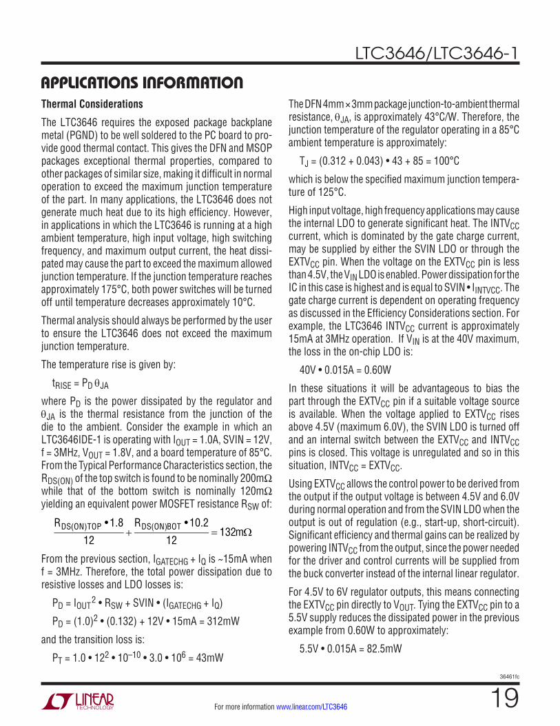
TYPICAL APPLICATIONS12V to 1.8V Output with 400kHz External Sync
Efficiency Curve 50mA to 1A Load Step
LOAD CURRENT (A)0.001
EFFI
CIEN
CY (%
)
0.1 1
3646 TA02b
00.01
100
10
20
30
40
50
60
70
80
90
PVIN
SVIN
RUN
INTVCC
ITH
RT
MODE/SYNC
EXTVCC
BOOST
SW
VON
VFB+ –
SWITCHCONTROL
400kHzEXTERNAL
CLOCK
LTC3646-10.1µF
L110µH
SGND PGND
22µF
0.6V226k
100k
RCOMP49.9k
3646 TA02a
4.7µF
CCOMP220pF
L1: WÜRTH WE-TPC-744-065-100
VIN12V 2Ω
2.2µF
CF4.7pF274k
100µF
137k
VOUT1.8V
40µs/DIV 3646 TA02c
VOUT100mV/DIV
AC-COUPLED
IL1A/DIV
ILOAD1A/DIV
LTC3646/LTC3646-1
2436461fc
For more information www.linear.com/LTC3646
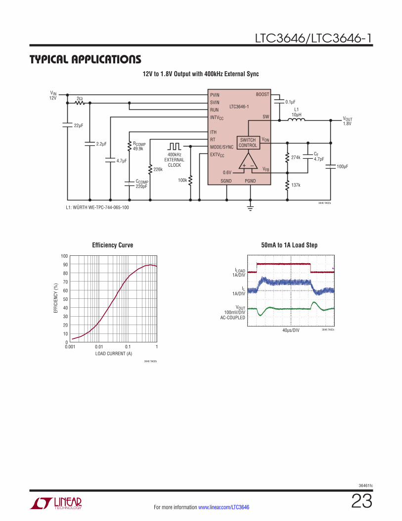
TYPICAL APPLICATIONS24V Input to 5V Output at 1MHz Frequency and EXTVCC
Efficiency Curve 50mA to 1A Load Step
PVIN
SVIN
RUN
INTVCC
PGOOD
ITH
RT
MODE/SYNC
EXTVCC
BOOST
SW
VON
VFB+ –
SWITCHCONTROL
LTC3646
100k
2Ω
L110µH
SGND PGND
0.1µF
487k
22µF
0.6V
90.9k
RCOMP100k
66.5k
3646 TA03a
COUT30µF
VOUT5V
20pF4.7µF
CCOMP33pF
VIN24V
2.2µF
LOAD CURRENT (A)0.001
EFFI
CIEN
CY (%
)
0.1 1
3646 TA03b
00.01
100
10
20
30
40
50
60
70
80
90
40µs/DIV 3646 TA03c
VOUT200mV/DIV
AC-COUPLED
IL11A/DIV
ILOAD1A/DIV

LTC3646/LTC3646-1
2536461fc
For more information www.linear.com/LTC3646
3.00 ±0.10(2 SIDES)
4.00 ±0.10(2 SIDES)
NOTE:1. DRAWING PROPOSED TO BE MADE VARIATION OF VERSION (WGED-3) IN JEDEC PACKAGE OUTLINE MO-2292. DRAWING NOT TO SCALE 3. ALL DIMENSIONS ARE IN MILLIMETERS4. DIMENSIONS OF EXPOSED PAD ON BOTTOM OF PACKAGE DO NOT INCLUDE MOLD FLASH. MOLD FLASH, IF PRESENT, SHALL NOT EXCEED 0.15mm ON ANY SIDE5. EXPOSED PAD SHALL BE SOLDER PLATED6. SHADED AREA IS ONLY A REFERENCE FOR PIN 1 LOCATION ON THE TOP AND BOTTOM OF PACKAGE
0.40 ±0.10
BOTTOM VIEW—EXPOSED PAD
1.70 ±0.10
0.75 ±0.05
R = 0.115TYP
R = 0.05TYP
3.00 REF
1.70 ±0.05
17
148
PIN 1TOP MARK
(SEE NOTE 6)
0.200 REF
0.00 – 0.05
(DE14) DFN 0806 REV B
PIN 1 NOTCHR = 0.20 OR0.35 × 45°CHAMFER
3.00 REF
RECOMMENDED SOLDER PAD PITCH AND DIMENSIONSAPPLY SOLDER MASK TO AREAS THAT ARE NOT SOLDERED
2.20 ±0.05
0.70 ±0.05
3.60 ±0.05
PACKAGEOUTLINE
0.25 ±0.05
0.25 ±0.050.50 BSC
3.30 ±0.05
3.30 ±0.10
0.50 BSC
DE Package14-Lead Plastic DFN (4mm × 3mm)
(Reference LTC DWG # 05-08-1708 Rev B)
PACKAGE DESCRIPTIONPlease refer to http://www.linear.com/designtools/packaging/ for the most recent package drawings.

LTC3646/LTC3646-1
2636461fc
For more information www.linear.com/LTC3646
PACKAGE DESCRIPTION
MSOP (MSE16) 0213 REV F
0.53 ±0.152(.021 ±.006)
SEATINGPLANE
0.18(.007)
1.10(.043)MAX
0.17 – 0.27(.007 – .011)
TYP
0.86(.034)REF
0.50(.0197)
BSC
16
16151413121110
1 2 3 4 5 6 7 8
9
9
1 8
NOTE:1. DIMENSIONS IN MILLIMETER/(INCH)2. DRAWING NOT TO SCALE3. DIMENSION DOES NOT INCLUDE MOLD FLASH, PROTRUSIONS OR GATE BURRS. MOLD FLASH, PROTRUSIONS OR GATE BURRS SHALL NOT EXCEED 0.152mm (.006") PER SIDE4. DIMENSION DOES NOT INCLUDE INTERLEAD FLASH OR PROTRUSIONS. INTERLEAD FLASH OR PROTRUSIONS SHALL NOT EXCEED 0.152mm (.006") PER SIDE5. LEAD COPLANARITY (BOTTOM OF LEADS AFTER FORMING) SHALL BE 0.102mm (.004") MAX6. EXPOSED PAD DIMENSION DOES INCLUDE MOLD FLASH. MOLD FLASH ON E-PAD SHALL NOT EXCEED 0.254mm (.010") PER SIDE.
0.254(.010) 0° – 6° TYP
DETAIL “A”
DETAIL “A”
GAUGE PLANE
5.10(.201)MIN
3.20 – 3.45(.126 – .136)
0.889 ±0.127(.035 ±.005)
RECOMMENDED SOLDER PAD LAYOUT
0.305 ±0.038(.0120 ±.0015)
TYP
0.50(.0197)
BSC
BOTTOM VIEW OFEXPOSED PAD OPTION
2.845 ±0.102(.112 ±.004)
2.845 ±0.102(.112 ±.004)
4.039 ±0.102(.159 ±.004)
(NOTE 3)
1.651 ±0.102(.065 ±.004)
1.651 ±0.102(.065 ±.004)
0.1016 ±0.0508(.004 ±.002)
3.00 ±0.102(.118 ±.004)
(NOTE 4)
0.280 ±0.076(.011 ±.003)
REF
4.90 ±0.152(.193 ±.006)
DETAIL “B”
DETAIL “B”CORNER TAIL IS PART OF
THE LEADFRAME FEATURE.FOR REFERENCE ONLY
NO MEASUREMENT PURPOSE
0.12 REF
0.35REF
MSE Package16-Lead Plastic MSOP, Exposed Die Pad
(Reference LTC DWG # 05-08-1667 Rev F)
Please refer to http://www.linear.com/designtools/packaging/ for the most recent package drawings.

LTC3646/LTC3646-1
2736461fc
For more information www.linear.com/LTC3646
Information furnished by Linear Technology Corporation is believed to be accurate and reliable. However, no responsibility is assumed for its use. Linear Technology Corporation makes no representa-tion that the interconnection of its circuits as described herein will not infringe on existing patent rights.
REVISION HISTORYREV DATE DESCRIPTION PAGE NUMBER
A 07/13 Changed '%' to '%/V’ regarding VREF Line Regulation in the Electrical Characteristics Table. 3
B 03/14 Clarified DescriptionClarified Operating Junction TemperatureClarified specificationsClarified graphClarified formulaClarified descriptionClarified Application drawings
12, 3, 4
35
1119
22, 28
C 08/15 Clarified Valley Switch Current LimitClarified Inductor Selection paragraphClarified Related Parts list
31128

LTC3646/LTC3646-1
2836461fc
For more information www.linear.com/LTC3646
Linear Technology Corporation1630 McCarthy Blvd., Milpitas, CA 95035-7417 (408) 432-1900 FAX: (408) 434-0507 www.linear.com LINEAR TECHNOLOGY CORPORATION 2012
LT 0815 REV C • PRINTED IN USA
RELATED PARTS
TYPICAL APPLICATION
Efficiency
28V Output at 500kHz Operating Frequency
LOAD CURRENT (A)0.001
EFFI
CIEN
CY (%
)
0.1 1
3646 TA04b
00.01
100
10
20
30
40
50
60
70
80
90
Burst Mode OPERATIONFORCED CONTINUOUS
PVIN
SVIN
RUN
INTVCC
PGOOD
ITH
RT
MODE/SYNC
EXTVCC
BOOST
SW
VON
VFB+ –
SWITCHCONTROL
LTC3646
100k
2Ω
L147µH
SGND PGND
0.1µF
487k
22µF
0.6V
180k
RCOMP402k
10.7k
3646 TA04a
COUT33µF
VOUT28V
4.7µF
CCOMP220pF
VIN40V
2.2µF
L1: WÜRTH WE-TPC-744-066-470
D1: DFLS 1200
PART NUMBER DESCRIPTION
VIN MIN (V)
VIN MAX (V)
VOUT MIN (V) IQ ISD PACKAGE
LT8609 42V, 2A, 95% Efficiency, 2.2MHz Synchronous MicroPower Step-Down DC/DC Converter with IQ = 2.5μA
3 42 0.8 2.5µA <1µA MSOP-10E
LTC3642 45V Input Capable with 60V Transient Protection, 50mA, Synchronous MicroPower Step-Down DC/DC Converter with IQ = 12μA
4.5 45, 60 Transient
0.8 12μA <1µA 3 × 3 DFN-8, MSOP-8E
LTC3631 45V Input Capable with 60V Transient Protection, 100mA, Synchronous MicroPower Step-Down DC/DC Converter with IQ = 12μA
4.5 45, 60 Transient
0.8 12μA <1µA 3 × 3 DFN-8, MSOP-8E
LTC3632 50V Input Capable with 60V Transient Protection, 20mA, Synchronous MicroPower Step-Down DC/DC Converter with IQ = 12μA
4.5 45, 60 Transient
0.8 12μA <1µA 3 × 3 DFN-8, MSOP-8E
LT8610 42V, 2.5A, 96% Efficiency, 2.2MHz Synchronous MicroPower Step-Down DC/DC Converter with IQ = 2.5μA
3.4 42 0.97 2.5µA <1µA MSOP-16E
LT8610A/AB 42V, 3.5A, 96% Efficiency, 2.2MHz Synchronous MicroPower Step-Down DC/DC Converter with IQ = 2.5μA
3.4 42 0.97 2.5µA <1µA MSOP-16E
LT8610AC-1 42V, 3.5A, 96% Efficiency, 2.2MHz Synchronous MicroPower Step-Down DC/DC Converter with IQ = 2.5μA
3 42 0.8 2.5µA <1µA MSOP-16E
LT8611 42V, 2.5A, 96% Efficiency, 2.2MHz Synchronous MicroPower Step-Down DC/DC Converter with IQ = 2.5μA and Input/Output Current Limit/Monitor
3.4 42 0.97 2.5µA <1µA 3 × 5 QFN-24
LT8620 65V, 2.5A, 96% Efficiency, 2.2MHz Synchronous MicroPower Step-Down DC/DC Converter with IQ = 2.5μA
3.4 65 0.97 2.5µA <1µA MSOP-16E 3 × 5 QFN-24
LT3991 55V, 1.2A, 2.2MHz High Efficiency MicroPower Step-Down DC/DC Converter with IQ = 2.8μA
4.3 38 1.2 2.8µA <1µA 3 × 3 DFN-10, MSOP-10E
LT3980 58V with Transient Protection to 80V, 2A (IOUT), 2.4MHz, High Efficiency Step-Down DC/DC Converter with Burst Mode Operation
3.6 58, Transient
to 80
0.78 85µA <1µA 3 × 4 DFN-16, MSOP-16E