40V P-Channel MOSFETs
5
40V P-Channel MOSFETs Symbol Parameter Rating Units VDS Drain-Source Voltage -40 V VGS Gate-Source Voltage ± 20 V ID Drain Current – Continuous (TC=25℃) -16 A Drain Current – Continuous (TC=100℃) -10 A IDM Drain Current – Pulsed 1 -64 A EAS Single Pulse Avalanche Energy 2 31 mJ IAS Single Pulse Avalanche Current 2 25 A PD Power Dissipation (TC=25℃) 32.9 W Power Dissipation – Derate above 25℃ 0.26 W/℃ TSTG Storage Temperature Range -50 to 150 ℃ TJ Operating Junction Temperature Range -50 to 150 ℃ Symbol Parameter Typ. Max. Unit Rθ JA Thermal Resistance Junction to ambient --- 62 ℃/W Rθ JC Thermal Resistance Junction to Case --- 3.8 ℃/W BVDSS RDSON ID -40V 45mΩ -16A These P-Channel enhancement mode power field effect transistors are using trench DMOS technology. This advanced technology has been especially tailored to minimize on-state resistance, provide superior switching performance, and withstand high energy pulse in the avalanche and commutation mode. These devices are well suited for high efficiency fast switching applications. -40V,-16A, RDS(ON) =45mΩ@VGS = -10V Improved dv/dt capability Fast switching Green Device Available General Description Features Applications Motor Drive Power Tools LED Lighting Absolute Maximum Ratings Tc=25℃ unless otherwise noted Thermal Characteristics TO252 Pin Configuration D S G D G S SEMICONDUCTOR TECHNICAL DATA FTK4909D 2018. 03. 22 1/5 Revision No : 0
Transcript of 40V P-Channel MOSFETs

40V P-Channel MOSFETs
Symbol Parameter Rating Units VDS Drain-Source Voltage -40 V
VGS Gate-Source Voltage ± 20 V
ID Drain Current – Continuous (TC=25℃) -16 A
Drain Current – Continuous (TC=100℃) -10 A
IDM Drain Current – Pulsed1 -64 A
EAS Single Pulse Avalanche Energy2 31 mJ
IAS Single Pulse Avalanche Current2 25 A
PD Power Dissipation (TC=25℃) 32.9 W
Power Dissipation – Derate above 25℃ 0.26 W/℃
TSTG Storage Temperature Range -50 to 150 ℃
TJ Operating Junction Temperature Range -50 to 150 ℃
Symbol Parameter Typ. Max. Unit RθJA Thermal Resistance Junction to ambient --- 62 ℃/W
RθJC Thermal Resistance Junction to Case --- 3.8 ℃/W
BVDSS RDSON ID
-40V 45mΩ -16A These P-Channel enhancement mode power field effect transistors are using trench DMOS technology. This advanced technology has been especially tailored to minimize on-state resistance, provide superior switching performance, and withstand high energy pulse in the avalanche and commutation mode. These devices are well suited for high efficiency fast switching applications.
-40V,-16A, RDS(ON) =45mΩ@VGS = -10V Improved dv/dt capability Fast switching Green Device Available
General Description
Features
Applications
Motor Drive Power Tools LED Lighting
Absolute Maximum Ratings Tc=25℃ unless otherwise noted
Thermal Characteristics
TO252 Pin Configuration
D
S G
D
G
S
SEMICONDUCTORTECHNICAL DATA FTK4909D
2018. 03. 22 1/5Revision No : 0
40V P-Channel MOSFETs
Off Characteristics
Symbol Parameter Conditions Min. Typ. Max. Unit BVDSS Drain-Source Breakdown Voltage VGS=0V , ID=-250uA -40 --- --- V
△BVDSS/△TJ BVDSS Temperature Coefficient Reference to 25℃ , ID=-1mA --- -0.05 --- V/℃
IDSS Drain-Source Leakage Current VDS=-40V , VGS=0V , TJ=25℃ --- --- -1 uA
VDS=-32V , VGS=0V , TJ=125℃ --- --- -10 uA
IGSS Gate-Source Leakage Current VGS=± 20V , VDS=0V --- --- ± 100 nA
On Characteristics
RDS(ON) Static Drain-Source On-Resistance VGS=-10V , ID=-10A --- 37 45 mΩ
VGS=-4.5V , ID=-6A --- 57 68 mΩ
VGS(th) Gate Threshold Voltage VGS=VDS , ID=-250uA
-1.2 -1.6 -2.5 V △VGS(th) VGS(th) Temperature Coefficient --- 5 --- mV/℃
gfs Forward Transconductance VDS=-10V , ID=-5A --- 7 --- S
Dynamic and switching Characteristics
Qg Total Gate Charge3,4 VDS=-20V , VGS=-4.5V , ID=-5A
--- 8.2 16 nC Qgs Gate-Source Charge3,4 --- 3.0 6
Qgd Gate-Drain Charge3,4 --- 2.5 5
Td(on) Turn-On Delay Time3,4 VDD=-20V , VGS=-10V , RG=6Ω
ID=-1A
--- 6.3 12
ns Tr Rise Time3,4 --- 7.2 14
Td(off) Turn-Off Delay Time3,4 --- 46 80
Tf Fall Time3,4 --- 14 27
Ciss Input Capacitance VDS=-25V , VGS=0V , F=1MHz
--- 825 1480 pF Coss Output Capacitance --- 68 130
Crss Reverse Transfer Capacitance --- 50 100
Symbol Parameter Conditions Min. Typ. Max. Unit
IS Continuous Source Current VG=VD=0V , Force Current
--- --- -16 A
ISM Pulsed Source Current --- --- -32 A
VSD Diode Forward Voltage VGS=0V , IS=-1A , TJ=25℃ --- --- -1 V
Note : 1. Repetitive Rating : Pulsed width limited by maximum junction temperature. 2. VDD=25V,VGS=10V,L=0.1mH,IAS=25A., Starting TJ=25℃ 3. The data tested by pulsed , pulse width ≦ 300us , duty cycle ≦ 2%. 4. Essentially independent of operating temperature.
Electrical Characteristics (TJ=25 , unless otherwise noted)
Drain - Source Diode Characteristics and Maximum Ratings
FTK4909D
2018. 03. 22 2/5Revision No : 0
40V P-Channel MOSFETs
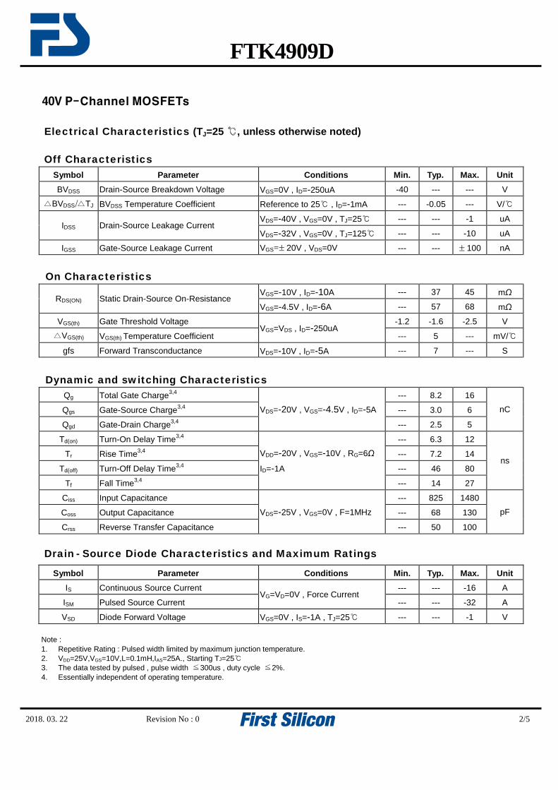
TC , Case Temperature (℃) Fig.1 Continuous Drain Current vs. TC
Nor
mal
ized
On
Res
istan
ce (m
Ω)
TJ , Junction Temperature (℃) Fig.2 Normalized RDSON vs. TJ
TJ , Junction Temperature (℃) Fig.3 Normalized Vth vs. TJ
-VG
S , G
ate
to S
ourc
e Vo
ltage
(V)
Qg , Gate Charge (nC) Fig.4 Gate Charge Waveform
Nor
mal
ized
The
rmal
Res
pons
e (RθJC
)
Square Wave Pulse Duration (s) Fig.5 Normalized Transient Impedance
- ID
, Con
tinuo
us D
rain
Cur
rent
(A)
-VDS , Drain to Source Voltage (V) Fig.6 Maximum Safe Operation Area
-ID ,
Con
tinuo
us D
rain
Cur
rent
( A)
Nor
mal
ized
Gat
e Th
resh
old
Volta
ge (V
)
FTK4909D
2018. 03. 22 3/5Revision No : 0
40V P-Channel MOSFETs
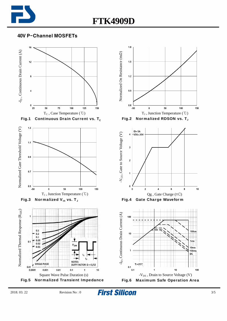
Td(on) Tr
Ton
Td(off) Tf
Toff
VDS
VGS
90%
10%
Fig.7 Switching Time Waveform Fig.8 EAS Waveform
2018. 03. 22 4/5Revision No : 0
FTK4909D
40V P-Channel MOSFETs
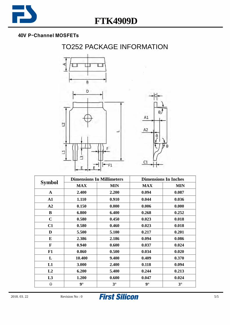
Symbol Dimensions In Millimeters Dimensions In Inches MAX MIN MAX MIN
A 2.400 2.200 0.094 0.087 A1 1.110 0.910 0.044 0.036 A2 0.150 0.000 0.006 0.000 B 6.800 6.400 0.268 0.252 C 0.580 0.450 0.023 0.018 C1 0.580 0.460 0.023 0.018 D 5.500 5.100 0.217 0.201 E 2.386 2.186 0.094 0.086 F 0.940 0.600 0.037 0.024
F1 0.860 0.500 0.034 0.020 L 10.400 9.400 0.409 0.370
L1 3.000 2.400 0.118 0.094 L2 6.200 5.400 0.244 0.213 L3 1.200 0.600 0.047 0.024 θ 9° 3° 9° 3°
TO252 PACKAGE INFORMATION
FTK4909D
2018. 03. 22 5/5Revision No : 0