LT1720/LT1721 - Linear Technology
28
LT1720/LT1721 1 17201fc TYPICAL APPLICATION DESCRIPTION Dual/Quad, 4.5ns, Single Supply 3V/5V Comparators with Rail-to-Rail Outputs The LT ® 1720/LT1721 are UltraFast TM dual/quad compara- tors optimized for single supply operation, with a supply voltage range of 2.7V to 6V. The input voltage range extends from 100mV below ground to 1.2V below the supply volt- age. Internal hysteresis makes the LT1720/LT1721 easy to use even with slow moving input signals. The rail-to-rail outputs directly interface to TTL and CMOS. Alternatively, the symmetric output drive can be harnessed for analog applications or for easy translation to other single supply logic levels. The LT1720 is available in three 8-pin packages; three pins per comparator plus power and ground. In addition to SO and MSOP packages, a 3mm × 3mm low profile (0.8mm) dual fine pitch leadless package (DFN) is available for space limited applications. The LT1721 is available in the 16-pin SSOP and S packages. The pinouts of the LT1720/LT1721 minimize parasitic effects by placing the most sensitive inputs (inverting) away from the outputs, shielded by the power rails. The LT1720/LT1721 are ideal for systems where small size and low power are paramount. 2.7V to 6V Crystal Oscillator with TTL/CMOS Output L, LT, LTC and LTM are registered trademarks of Linear Technology Corporation. UltaFast is a trademark of Linear Technology Corporation. All other trademarks are the property of their respective owners. FEATURES APPLICATIONS n High Speed Differential Line Receiver n Crystal Oscillator Circuits n Window Comparators n Threshold Detectors/Discriminators n Pulse Stretchers n Zero-Crossing Detectors n High Speed Sampling Circuits n UltraFast: 4.5ns at 20mV Overdrive 7ns at 5mV Overdrive n Low Power: 4mA per Comparator n Optimized for 3V and 5V Operation n Pinout Optimized for High Speed Ease of Use n Input Voltage Range Extends 100mV Below Negative Rail n TTL/CMOS Compatible Rail-to-Rail Outputs n Internal Hysteresis with Specified Limits n Low Dynamic Current Drain; 15μA/(V-MHz), Dominated by Load In Most Circuits n Tiny 3mm × 3mm × 0.75mm DFN Package (LT1720) Propagation Delay vs Overdrive – + C1 1/2 LT1720 2.7V TO 6V 2k 620Ω 220Ω 1MHz TO 10MHz CRYSTAL (AT-CUT) 2k 17201 TA01 0.1μF 1.8k OUTPUT GROUND CASE OVERDRIVE (mV) 0 DELAY (ns) 30 50 17201 TA02 10 20 40 8 7 6 5 4 3 2 1 0 25°C V STEP = 100mV V CC = 5V C LOAD = 10pF RISING EDGE (t PDLH ) FALLING EDGE (t PDHL )
Transcript of LT1720/LT1721 - Linear Technology

LT1720/LT1721
117201fc
TYPICAL APPLICATION
DESCRIPTION
Dual/Quad, 4.5ns, SingleSupply 3V/5V Comparators
with Rail-to-Rail Outputs
The LT®1720/LT1721 are UltraFastTM dual/quad compara-tors optimized for single supply operation, with a supply voltage range of 2.7V to 6V. The input voltage range extends from 100mV below ground to 1.2V below the supply volt-age. Internal hysteresis makes the LT1720/LT1721 easy to use even with slow moving input signals. The rail-to-rail outputs directly interface to TTL and CMOS. Alternatively, the symmetric output drive can be harnessed for analog applications or for easy translation to other single supply logic levels.
The LT1720 is available in three 8-pin packages; three pins per comparator plus power and ground. In addition to SO and MSOP packages, a 3mm × 3mm low profi le (0.8mm) dual fi ne pitch leadless package (DFN) is available for space limited applications. The LT1721 is available in the 16-pin SSOP and S packages.
The pinouts of the LT1720/LT1721 minimize parasitic effects by placing the most sensitive inputs (inverting) away from the outputs, shielded by the power rails. The LT1720/LT1721 are ideal for systems where small size and low power are paramount.
2.7V to 6V Crystal Oscillator with TTL/CMOS Output
L, LT, LTC and LTM are registered trademarks of Linear Technology Corporation. UltaFast is a trademark of Linear Technology Corporation. All other trademarks are the property of their respective owners.
FEATURES
APPLICATIONSn High Speed Differential Line Receivern Crystal Oscillator Circuitsn Window Comparatorsn Threshold Detectors/Discriminatorsn Pulse Stretchersn Zero-Crossing Detectorsn High Speed Sampling Circuits
n UltraFast: 4.5ns at 20mV Overdrive 7ns at 5mV Overdriven Low Power: 4mA per Comparator n Optimized for 3V and 5V Operationn Pinout Optimized for High Speed Ease of Usen Input Voltage Range Extends 100mV Below Negative Railn TTL/CMOS Compatible Rail-to-Rail Outputsn Internal Hysteresis with Specifi ed Limitsn Low Dynamic Current Drain; 15μA/(V-MHz), Dominated by Load In Most Circuitsn Tiny 3mm × 3mm × 0.75mm DFN Package (LT1720)
Propagation Delay vs Overdrive
–
+C1
1/2 LT1720
2.7V TO 6V
2k
620Ω
220Ω
1MHz TO 10MHzCRYSTAL (AT-CUT)
2k17201 TA01
0.1μF 1.8k
OUTPUT
GROUNDCASE
OVERDRIVE (mV)
0
DELA
Y (
ns)
30 50
17201 TA02
10 20 40
8
7
6
5
4
3
2
1
0
25°CVSTEP = 100mVVCC = 5VCLOAD = 10pF
RISING EDGE(tPDLH)
FALLING EDGE(tPDHL)

LT1720/LT1721
217201fc
ABSOLUTE MAXIMUM RATINGSSupply Voltage, VCC to GND ........................................7VInput Current ....................................................... ±10mAOutput Current (Continuous) ............................. ±20mAJunction Temperature .......................................... 150°C (DD Package) .................................................... 125°CLead Temperature (Soldering, 10 sec) .................. 300°C
(Note 1)
TOP VIEW
DD PACKAGE8-LEAD (3mm 3mm) PLASTIC DFN
5
6
7
8
4
3
2
1+IN A
–IN A
–IN B
+IN B
VCC
OUT A
OUT B
GND
9
TJMAX = 125°C, θJA = 160°C/WUNDERSIDE METAL INTERNALLY
CONNECTED TO GND
1
2
3
4
+IN A
–IN A
–IN B
+IN B
8
7
6
5
VCCOUT A
OUT B
GND
TOP VIEW
MS8 PACKAGE8-LEAD PLASTIC MSOP
TJMAX = 150°C, θJA = 230°C/W
TOP VIEW
VCC
OUT A
OUT B
GND
+IN A
–IN A
–IN B
+IN B
S8 PACKAGE8-LEAD PLASTIC SO
1
2
3
4
8
7
6
5
TJMAX = 150°C, θJA = 200°C/W
1
2
3
4
5
6
7
8
TOP VIEW
GN PACKAGE16-LEAD NARROW
PLASTIC SSOP
S PACKAGE16-LEAD PLASTIC SO
16
15
14
13
12
11
10
9
–IN A
+IN A
GND
OUT A
OUT B
GND
+IN B
–IN B
–IN D
+IN D
VCC
OUT D
OUT C
VCC
+IN C
–IN C
TJMAX = 150°C, θJA = 135°C/W (GN)TJMAX = 150°C, θJA = 115°C/W (S)
PIN CONFIGURATION
Storage Temperature Range ................... –65°C to 150°C (DD Package) ..................................... –65°C to 125°COperating Temperature Range C Grade ................................................... 0°C to 70°C I Grade ............................................... –40°C to 85°C
LT1720/LT1721
317201fc
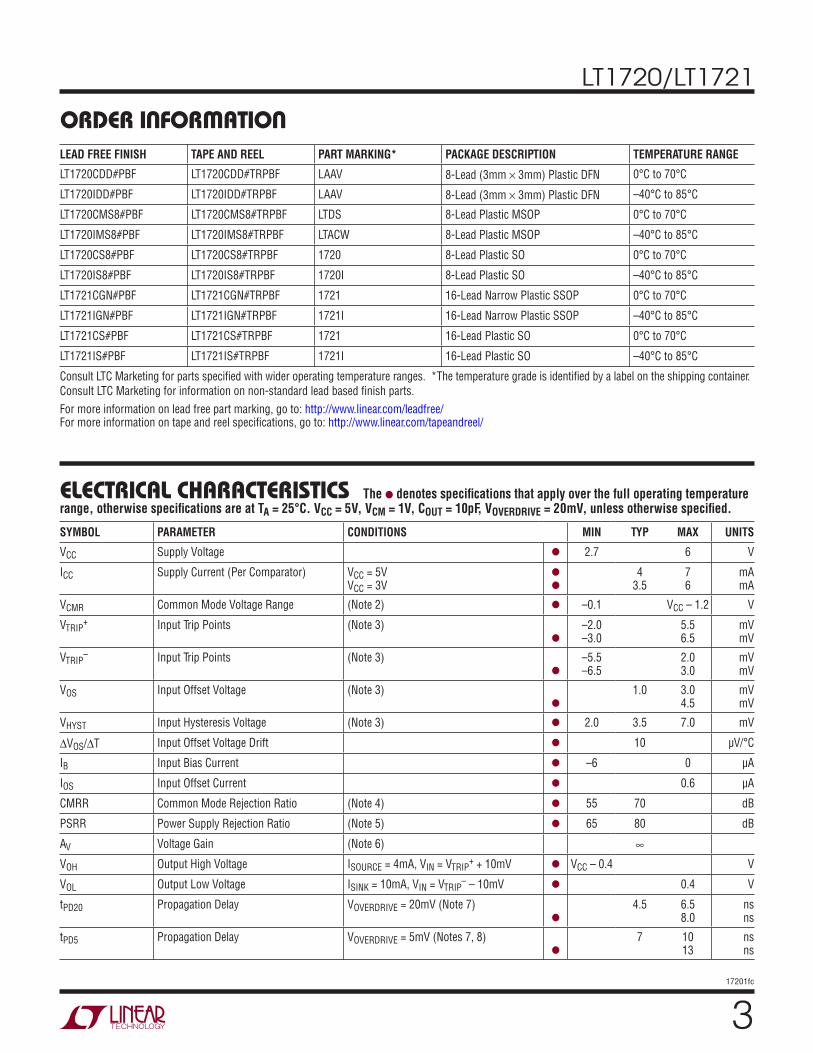
ELECTRICAL CHARACTERISTICS
SYMBOL PARAMETER CONDITIONS MIN TYP MAX UNITS
VCC Supply Voltage l 2.7 6 V
ICC Supply Current (Per Comparator) VCC = 5VVCC = 3V
l
l
43.5
76
mAmA
VCMR Common Mode Voltage Range (Note 2) l –0.1 VCC – 1.2 V
VTRIP+ Input Trip Points (Note 3)
l
–2.0–3.0
5.56.5
mVmV
VTRIP– Input Trip Points (Note 3)
l
–5.5–6.5
2.03.0
mVmV
VOS Input Offset Voltage (Note 3)l
1.0 3.04.5
mVmV
VHYST Input Hysteresis Voltage (Note 3) l 2.0 3.5 7.0 mV
ΔVOS/ΔT Input Offset Voltage Drift l 10 μV/°C
IB Input Bias Current l –6 0 μA
IOS Input Offset Current l 0.6 μA
CMRR Common Mode Rejection Ratio (Note 4) l 55 70 dB
PSRR Power Supply Rejection Ratio (Note 5) l 65 80 dB
AV Voltage Gain (Note 6) ∞
VOH Output High Voltage ISOURCE = 4mA, VIN = VTRIP+ + 10mV l VCC – 0.4 V
VOL Output Low Voltage ISINK = 10mA, VIN = VTRIP– – 10mV l 0.4 V
tPD20 Propagation Delay VOVERDRIVE = 20mV (Note 7)l
4.5 6.58.0
nsns
tPD5 Propagation Delay VOVERDRIVE = 5mV (Notes 7, 8)l
7 1013
nsns
The l denotes specifi cations that apply over the full operating temperature range, otherwise specifi cations are at TA = 25°C. VCC = 5V, VCM = 1V, COUT = 10pF, VOVERDRIVE = 20mV, unless otherwise specifi ed.
ORDER INFORMATIONLEAD FREE FINISH TAPE AND REEL PART MARKING* PACKAGE DESCRIPTION TEMPERATURE RANGE
LT1720CDD#PBF LT1720CDD#TRPBF LAAV 8-Lead (3mm × 3mm) Plastic DFN 0°C to 70°C
LT1720IDD#PBF LT1720IDD#TRPBF LAAV 8-Lead (3mm × 3mm) Plastic DFN –40°C to 85°C
LT1720CMS8#PBF LT1720CMS8#TRPBF LTDS 8-Lead Plastic MSOP 0°C to 70°C
LT1720IMS8#PBF LT1720IMS8#TRPBF LTACW 8-Lead Plastic MSOP –40°C to 85°C
LT1720CS8#PBF LT1720CS8#TRPBF 1720 8-Lead Plastic SO 0°C to 70°C
LT1720IS8#PBF LT1720IS8#TRPBF 1720I 8-Lead Plastic SO –40°C to 85°C
LT1721CGN#PBF LT1721CGN#TRPBF 1721 16-Lead Narrow Plastic SSOP 0°C to 70°C
LT1721IGN#PBF LT1721IGN#TRPBF 1721I 16-Lead Narrow Plastic SSOP –40°C to 85°C
LT1721CS#PBF LT1721CS#TRPBF 1721 16-Lead Plastic SO 0°C to 70°C
LT1721IS#PBF LT1721IS#TRPBF 1721I 16-Lead Plastic SO –40°C to 85°C
Consult LTC Marketing for parts specifi ed with wider operating temperature ranges. *The temperature grade is identifi ed by a label on the shipping container.
Consult LTC Marketing for information on non-standard lead based fi nish parts.
For more information on lead free part marking, go to: http://www.linear.com/leadfree/ For more information on tape and reel specifi cations, go to: http://www.linear.com/tapeandreel/
LT1720/LT1721
417201fc
TYPICAL PERFORMANCE CHARACTERISTICS
SUPPLY VOLTAGE (V)
2.5
VO
S A
ND
TR
IP P
OIN
T V
OLTA
GE (
mV
)
3
2
1
0
–1
–2
–34.0 5.0
17201 G01
3.0 3.5 4.5 5.5 6.0
VTRIP+
VOS
VTRIP–
25°CVCM = 1V
TEMPERATURE (°C)
–3
VO
SA
ND
TR
IP P
OIN
T V
OLTA
GE (
mV
)
–1
1
3
–2
0
2
–25 25 100
17201 G02
–50 0 50 75 125
VTRIP+
VOS
VTRIP–
TEMPERATURE (°C)
–50
3.6
3.8
4.2
25 75
17201 G03
0.2
0
–25 0 50 100 125
–0.2
–0.4
4.0
CO
MM
ON
MO
DE I
NP
UT V
OLTA
GE (
V)
VCC = 5V
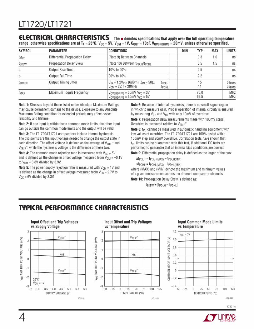
Input Offset and Trip Voltages vs Supply Voltage
Input Offset and Trip Voltages vs Temperature
Input Common Mode Limitsvs Temperature
Note 1: Stresses beyond those listed under Absolute Maximum Ratings
may cause permanent damage to the device. Exposure to any Absolute
Maximum Rating condition for extended periods may affect device
reliability and lifetime.
Note 2: If one input is within these common mode limits, the other input
can go outside the common mode limits and the output will be valid.
Note 3: The LT1720/LT1721 comparators include internal hysteresis.
The trip points are the input voltage needed to change the output state in
each direction. The offset voltage is defi ned as the average of VTRIP+ and
VTRIP–, while the hysteresis voltage is the difference of these two.
Note 4: The common mode rejection ratio is measured with VCC = 5V
and is defi ned as the change in offset voltage measured from VCM = –0.1V
to VCM = 3.8V, divided by 3.9V.
Note 5: The power supply rejection ratio is measured with VCM = 1V and
is defi ned as the change in offset voltage measured from VCC = 2.7V to
VCC = 6V, divided by 3.3V.
ELECTRICAL CHARACTERISTICS The l denotes specifi cations that apply over the full operating temperature range, otherwise specifi cations are at TA = 25°C. VCC = 5V, VCM = 1V, COUT = 10pF, VOVERDRIVE = 20mV, unless otherwise specifi ed.
SYMBOL PARAMETER CONDITIONS MIN TYP MAX UNITS
ΔtPD Differential Propagation Delay (Note 9) Between Channels 0.3 1.0 ns
tSKEW Propagation Delay Skew (Note 10) Between tPDLH/tPDHL 0.5 1.5 ns
tr Output Rise Time 10% to 90% 2.5 ns
tf Output Fall Time 90% to 10% 2.2 ns
tJITTER Output Timing Jitter VIN = 1.2VP-P (6dBm), ZIN = 50Ω tPDLHVCM = 2V, f = 20MHz tPDHL
1511
psRMSpsRMS
fMAX Maximum Toggle Frequency VOVERDRIVE = 50mV, VCC = 3VVOVERDRIVE = 50mV, VCC = 5V
70.062.5
MHzMHz
Note 6: Because of internal hysteresis, there is no small-signal region
in which to measure gain. Proper operation of internal circuity is ensured
by measuring VOH and VOL with only 10mV of overdrive.
Note 7: Propagation delay measurements made with 100mV steps.
Overdrive is measured relative to VTRIP±.
Note 8: tPD cannot be measured in automatic handling equipment with
low values of overdrive. The LT1720/LT1721 are 100% tested with a
100mV step and 20mV overdrive. Correlation tests have shown that
tPD limits can be guaranteed with this test, if additional DC tests are
performed to guarantee that all internal bias conditions are correct.
Note 9: Differential propagation delay is defi ned as the larger of the two:
ΔtPDLH = tPDLH(MAX) – tPDLH(MIN)
ΔtPDHL = tPDHL(MAX) – tPDHL(MIN)
where (MAX) and (MIN) denote the maximum and minimum values
of a given measurement across the different comparator channels.
Note 10: Propagation Delay Skew is defi ned as:
tSKEW = |tPDLH – tPDHL|
LT1720/LT1721
517201fc
TYPICAL PERFORMANCE CHARACTERISTICS
DIFFERENTIAL INPUT VOLTAGE (V)
–5–7
INP
UT C
UR
REN
T (
μA
)
–6
–4
–3
–2
1 2 3 4
2
17201 G04
–5
–4 –3 –2 –1 0 5
–1
0
125°CVCC = 5V
TEMPERATURE (˚C)
–50
QU
IES
CEN
T S
UP
PLY
CU
RR
EN
T P
ER
CO
MP
AR
ATO
R (
mA
)
5.5
25
17201 G05
4.0
3.0
–25 0 50
2.5
2.0
6.0
5.0
4.5
3.5
75 100 125
VCC = 5V
VCC = 3V
SUPPLY VOLTAGE (V)
00
SU
PP
LY
CU
RR
EN
T P
ER
CO
MP
AR
ATO
R (
mA
)
4
7
2 4 5
17201 G06
3
2
1
6
5
1 3 6 7
25°C
125°C
–55°C
OUTPUT LOAD CAPACITANCE (pF)
0
DELA
Y (
ns)
30 50
17201 G07
10 20 40
9
8
7
6
5
4
3
2
1
0
25°CVSTEP = 100mVOVERDRIVE = 20mVVCC = 5V
RISING EDGE(tPDLH)
FALLING EDGE(tPDHL)
TEMPERATURE (°C)
–50
PR
OP
AG
ATIO
N D
ELA
Y (
ns)
7.5
25
17201 G08
6.0
5.0
–25 0 50
4.5
4.0
8.0
7.0
6.5
5.5
75 100 125
VCC = 3V
VCC = 3V
VCC = 5V
VCC = 5V
tPDLHVCM = 1VVSTEP = 100mVCLOAD = 10pF
OVERDRIVE = 5mV
OVERDRIVE = 20mV
SUPPLY VOLTAGE (V)
2.5
4.5
DELA
Y (
ns)
5.0
4.04.0 5.0
17201 G09
3.0 3.5 4.5 5.5 6.0
RISING EDGE(tPDLH)
FALLING EDGE(tPDHL)
25°CVSTEP = 100mVOVERDRIVE = 20mVCLOAD = 10pF
OUTPUT SINK CURRENT (mA)
0
OU
TP
UT V
OLTA
GE (
V)
0.3
0.4
16
17201 G10
0.2
0.14 8 12 20
0.5
125°C
25°C
125°CVCC = 2.7V
VCC = 5VVCM = 1VVIN = –15mV
–55°C
OUTPUT SOURCE CURRENT (mA)
0
OU
TP
UT V
OLTA
GE R
ELA
TIV
E T
O V
CC (
V)
–0.4
–0.2
0.0
16
17201 G11
–0.6
–0.8
–1.04 8 12 20
125°C
–55°C25°C
25°CVCC = 2.7V
VCC = 5VVCM = 1VVIN = 15mV
FREQUENCY (MHz)
0
7
8
10
30
NO LOAD
17201 G12
6
5
10 20 40
4
3
9
SU
PP
LY
CU
RR
EN
T P
ER
CO
MP
AR
ATO
R (
mA
)
25°CVCC = 5V
CLOAD = 20pF
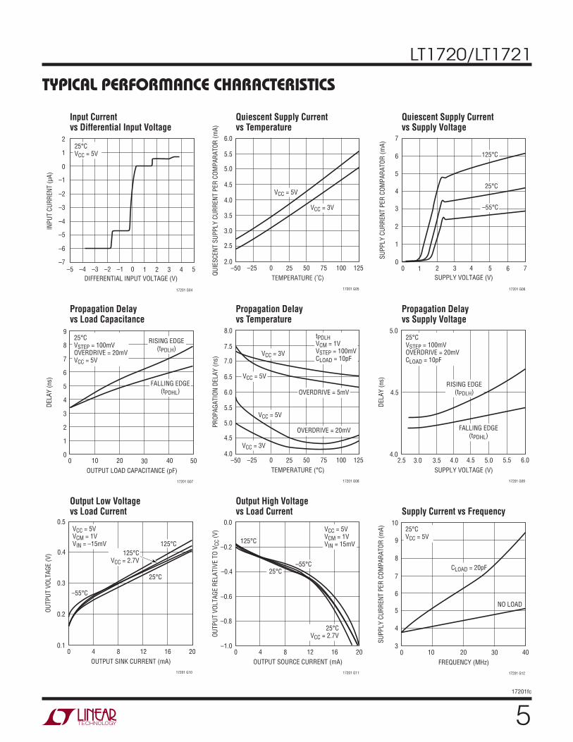
Propagation Delayvs Load Capacitance
Propagation Delay vs Temperature
Propagation Delayvs Supply Voltage
Output Low Voltage vs Load Current
Output High Voltagevs Load Current Supply Current vs Frequency
Input Current vs Differential Input Voltage
Quiescent Supply Currentvs Temperature
Quiescent Supply Currentvs Supply Voltage
LT1720/LT1721
617201fc
PIN FUNCTIONSLT1720
+IN A (Pin 1): Noninverting Input of Comparator A.
–IN A (Pin 2): Inverting Input of Comparator A.
–IN B (Pin 3): Inverting Input of Comparator B.
+IN B (Pin 4): Noninverting Input of Comparator B.
GND (Pin 5): Ground.
OUT B (Pin 6): Output of Comparator B.
OUT A (Pin 7): Output of Comparator A.
VCC (Pin 8): Positive Supply Voltage.
LT1721
–IN A (Pin 1): Inverting Input of Comparator A.
+IN A (Pin 2): Noninverting Input of Comparator A.
GND (Pins 3, 6): Ground.
OUT A (Pin 4): Output of Comparator A.
OUT B (Pin 5): Output of Comparator B.
+IN B (Pin 7): Noninverting Input of Comparator B.
–IN B (Pin 8): Inverting Input of Comparator B.
–IN C (Pin 9): Inverting Input of Comparator C.
+IN C (Pin 10): Noninverting Input of Comparator C.
VCC (Pins 11, 14): Positive Supply Voltage.
OUT C (Pin 12): Output of Comparator C.
OUT D (Pin 13): Output of Comparator D.
+IN D (Pin 15): Noninverting Input of Comparator D.
–IN D (Pin 16): Inverting Input of Comparator D.
LT1720/LT1721
717201fc
TEST CIRCUITS
+
–
+
–
+–
–
+
DUT1/2 LT1720 OR
1/4 LT1721
15VP-PBANDWIDTH-LIMITED
TRIANGLE WAVE~1kHz
LTC203
1/2 LT111250Ω
100k 100k
2.4k
10nF 1μF
0.15μF
1/2 LT1638
1/2 LT1638
100k
100k
200k
10k
10k
1000 VHYST
1000 VTRIP+
1000 VTRIP–
1000 VOS
0.1μF
50Ω
50k
VCM
VCC
+–
1/2 LT1112
17201 TC01
10nF 1μF
NOTES: LT1638, LT1112, LTC203s ARE POWERED FROM 15V. 200kW PULL-DOWN PROTECTS LTC203 LOGIC INPUTS WHEN DUT IS NOT POWERED
15 3 214
16
9
1
8
10 6 711
LTC203
2 14 153
1
8
16
9
7 11 106
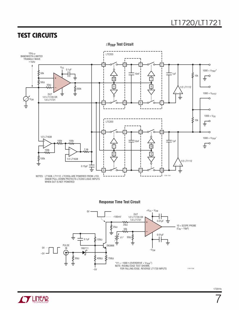
±VTRIP Test Circuit
Response Time Test Circuit
–
+
–3V
–100mV
–5V
PULSEIN0V
0V
50Ω
1N5711
400Ω
130Ω
25Ω
50Ω
+VCC – VCM
–VCM
50k
DUT1/2 LT1720 OR
1/4 LT1721
25Ω
0.1μF
17201 TC02
10 SCOPE PROBE(CIN ≈ 10pF)
0.01μF
0.01μF
750Ω
2N3866
V1*
*V1 = –1000 • (OVERDRIVE VTRIP+)
NOTE: RISING EDGE TEST SHOWN. FOR FALLING EDGE, REVERSE LT1720 INPUTS

LT1720/LT1721
817201fc
Input Voltage Considerations
The LT1720/LT1721 are specifi ed for a common mode range of –100mV to 3.8V when used with a single 5V supply. In general the common mode range is 100mV below ground to 1.2V below VCC. The criterion for this common mode limit is that the output still responds correctly to a small differential input signal. Also, if one input is within the common mode limit, the other input signal can go outside the common mode limits, up to the absolute maximum limits (a diode drop past either rail at 10mA input current) and the output will retain the correct polarity.
When either input signal falls below the negative common mode limit, the internal PN diode formed with the substrate can turn on, resulting in signifi cant current fl ow through the die. An external Schottky clamp diode between the input and the negative rail can speed up recovery from negative overdrive by preventing the substrate diode from turning on.
When both input signals are below the negative common mode limit, phase reversal protection circuitry prevents false output inversion to at least –400mV common mode. However, the offset and hysteresis in this mode will increase dramatically, to as much as 15mV each. The input bias currents will also increase.
When both input signals are above the positive common mode limit, the input stage will become debiased and the output polarity will be random. However, the internal hysteresis will hold the output to a valid logic level, and because the biasing of each comparator is completely independent, there will be no impact on any other com-parator. When at least one of the inputs returns to within the common mode limits, recovery from this state will take as long as 1μs.
The propagation delay does not increase signifi cantly when driven with large differential voltages. However, with low levels of overdrive, an apparent increase may be seen with large source resistances due to an RC delay caused by the 2pF typical input capacitance.
APPLICATIONS INFORMATIONInput Protection
The input stage is protected against damage from large differential signals, up to and beyond a differential voltage equal to the supply voltage, limited only by the absolute maximum currents noted. External input protection cir-cuitry is only needed if currents would otherwise exceed these absolute maximums. The internal catch diodes can conduct current up to these rated maximums without latchup, even when the supply voltage is at the absolute maximum rating.
The LT1720/LT1721 input stage has general purpose internal ESD protection for the human body model. For use as a line receiver, additional external protection may be required. As with most integrated circuits, the level of immunity to ESD is much greater when residing on a printed circuit board where the power supply decoupling capacitance will limit the voltage rise caused by an ESD pulse.
Unused Inputs
The inputs of any unused compartor should be tied off in a way that defi nes the output logic state. The easiest way to do this is to tie IN+ to VCC and IN– to GND.
Input Bias Current
Input bias current is measured with both inputs held at 1V. As with any PNP differential input stage, the LT1720/LT1721 bias current fl ows out of the device. With a differential input voltage of even just 100mV or so, there will be zero bias current into the higher of the two inputs, while the current fl owing out of the lower input will be twice the measured bias current. With more than two diode drops of differential input voltage, the LT1720/LT1721’s input protection circuitry activates, and current out of the lower input will increase an additional 30% and there will be a small bias current into the higher of the two input pins, of 4μA or less. See the Typical Performance curve “Input Current vs Differential Input Voltage.”

LT1720/LT1721
917201fc
High Speed Design Considerations
Application of high speed comparators is often plagued by oscillations. The LT1720/LT1721 have 4mV of internal hysteresis, which will prevent oscillations as long as parasitic output to input feedback is kept below 4mV. However, with the 2V/ns slew rate of the LT1720/LT1721 outputs, a 4mV step can be created at a 100Ω input source with only 0.02pF of output to input coupling. The pinouts of the LT1720/LT1721 have been arranged to minimize problems by placing the most sensitive inputs (invert-ing) away from the outputs, shielded by the power rails. The input and output traces of the circuit board should also be separated, and the requisite level of isolation is readily achieved if a topside ground plane runs between the outputs and the inputs. For multilayer boards where the ground plane is internal, a topside ground or supply trace should be run between the inputs and outputs, as illustrated in Figure 1.
APPLICATIONS INFORMATIONAlthough both VCC pins are electrically shorted internal to the LT1721, they must be shorted together externally as well in order for both to function as shields. The same is true for the two GND pins.
The supply bypass should include an adjacent 10nF ce-ramic capacitor and a 2.2μF tantalum capacitor no farther than 5cm away; use more capacitance if driving more than 4mA loads. To prevent oscillations, it is helpful to balance the impedance at the inverting and noninverting inputs; source impedances should be kept low, preferably 1kΩ or less.
The outputs of the LT1720/LT1721 are capable of very high slew rates. To prevent overshoot, ringing and other problems with transmission line effects, keep the output traces shorter than 10cm, or be sure to terminate the lines to maintain signal integrity. The LT1720/LT1721 can drive DC terminations of 250Ω or more, but lower characteristic impedance traces can be driven with series termination or AC termination topologies.
Hysteresis
The LT1720/LT1721 include internal hysteresis, which makes them easier to use than many other comparable speed comparators.
The input-output transfer characteristic is illustrated in Figure 2 showing the defi nitions of VOS and VHYST based upon the two measurable trip points. The hysteresis band makes the LT1720/LT1721 well behaved, even with slowly moving inputs.
Figure 1. Typical Topside Metal for Multilayer PCB Layouts
17201 F01
(b)(a)
Figure 1a shows a typical topside layout of the LT1720 on such a multilayer board. Shown is the topside metal etch including traces, pin escape vias, and the land pads for an SO-8 LT1720 and its adjacent X7R 10nF bypass capacitor in a 1206 case.
The ground trace from Pin 5 runs under the device up to the bypass capacitor, shielding the inputs from the out-puts. Note the use of a common via for the LT1720 and the bypass capacitor, which minimizes interference from high frequency energy running around the ground plane or power distribution traces.
Figure 1b shows a typical topside layout of the LT1721 on a multilayer board. In this case, the power and ground traces have been extended to the bottom of the device solely to act as high frequency shields between input and output traces.
Figure 2. Hysteresis I/O Characteristics
VHYST
(= VTRIP+ – VTRIP
–)
VHYST/2
VOL
17201 F02
VOH
VTRIP–
VTRIP+
VIN = VIN+ – VIN
–
VTRIP+ + VTRIP
–
2VOS =
VO
UT
0
LT1720/LT1721
1017201fc
The exact amount of hysteresis will vary from part to part as indicated in the specifi cations table. The hysteresis level will also vary slightly with changes in supply voltage and common mode voltage. A key advantage of the LT1720/LT1721 is the signifi cant reduction in these effects, which is important whenever an LT1720/LT1721 is used to detect a threshold crossing in one direction only. In such a case, the relevant trip point will be all that matters, and a stable offset voltage with an unpredictable level of hysteresis, as seen in competing comparators, is of little value. The LT1720/LT1721 are many times better than prior compara-tors in these regards. In fact, the CMRR and PSRR tests are performed by checking for changes in either trip point to the limits indicated in the specifi cations table. Because the offset voltage is the average of the trip points, the CMRR and PSRR of the offset voltage is therefore guaranteed to be at least as good as those limits. This more stringent test also puts a limit on the common mode and power supply dependence of the hysteresis voltage.
Additional hysteresis may be added externally. The rail-to-rail outputs of the LT1720/LT1721 make this more predictable than with TTL output comparators due to the LT1720/LT1721’s small variability of VOH (output high voltage).
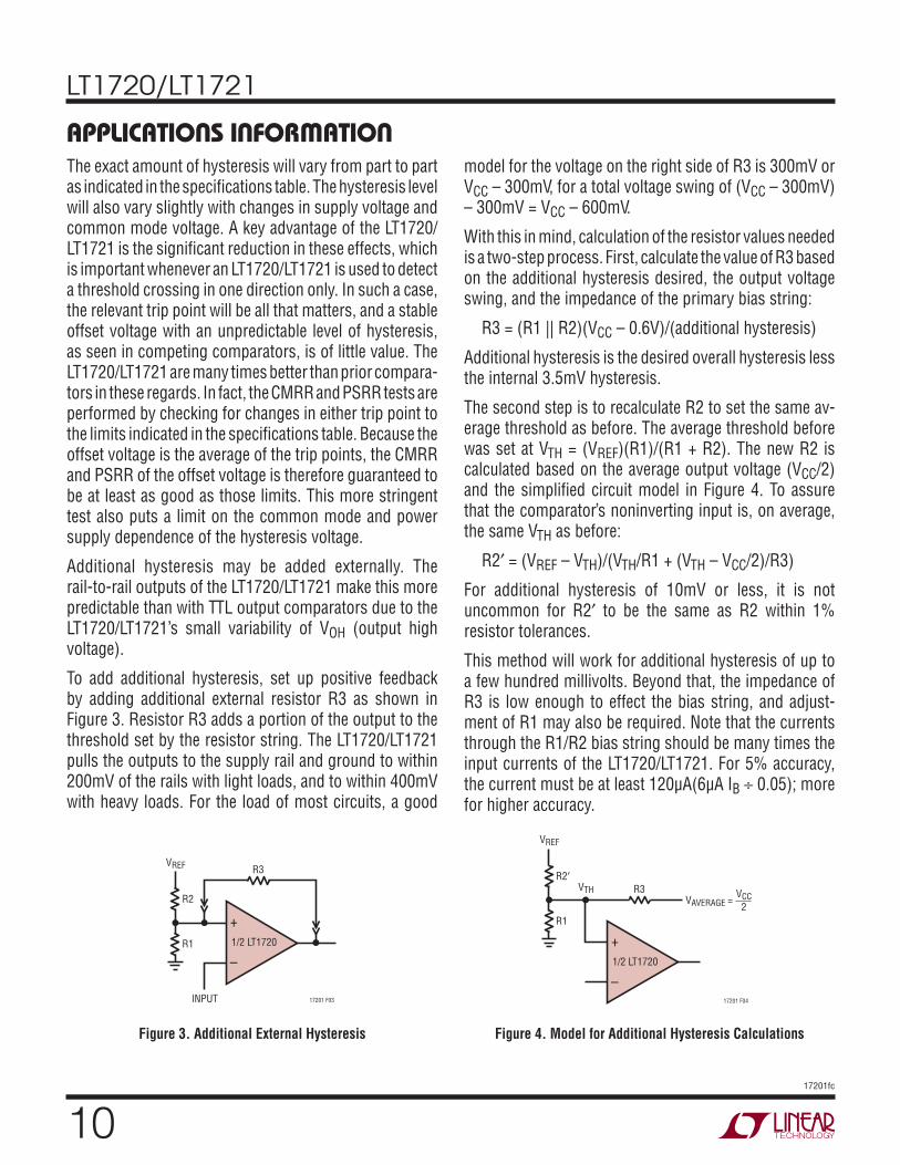
To add additional hysteresis, set up positive feedback by adding additional external resistor R3 as shown in Figure 3. Resistor R3 adds a portion of the output to the threshold set by the resistor string. The LT1720/LT1721 pulls the outputs to the supply rail and ground to within 200mV of the rails with light loads, and to within 400mV with heavy loads. For the load of most circuits, a good
APPLICATIONS INFORMATIONmodel for the voltage on the right side of R3 is 300mV or VCC – 300mV, for a total voltage swing of (VCC – 300mV) – 300mV = VCC – 600mV.
With this in mind, calculation of the resistor values needed is a two-step process. First, calculate the value of R3 based on the additional hysteresis desired, the output voltage swing, and the impedance of the primary bias string:
R3 = (R1 || R2)(VCC – 0.6V)/(additional hysteresis)
Additional hysteresis is the desired overall hysteresis less the internal 3.5mV hysteresis.
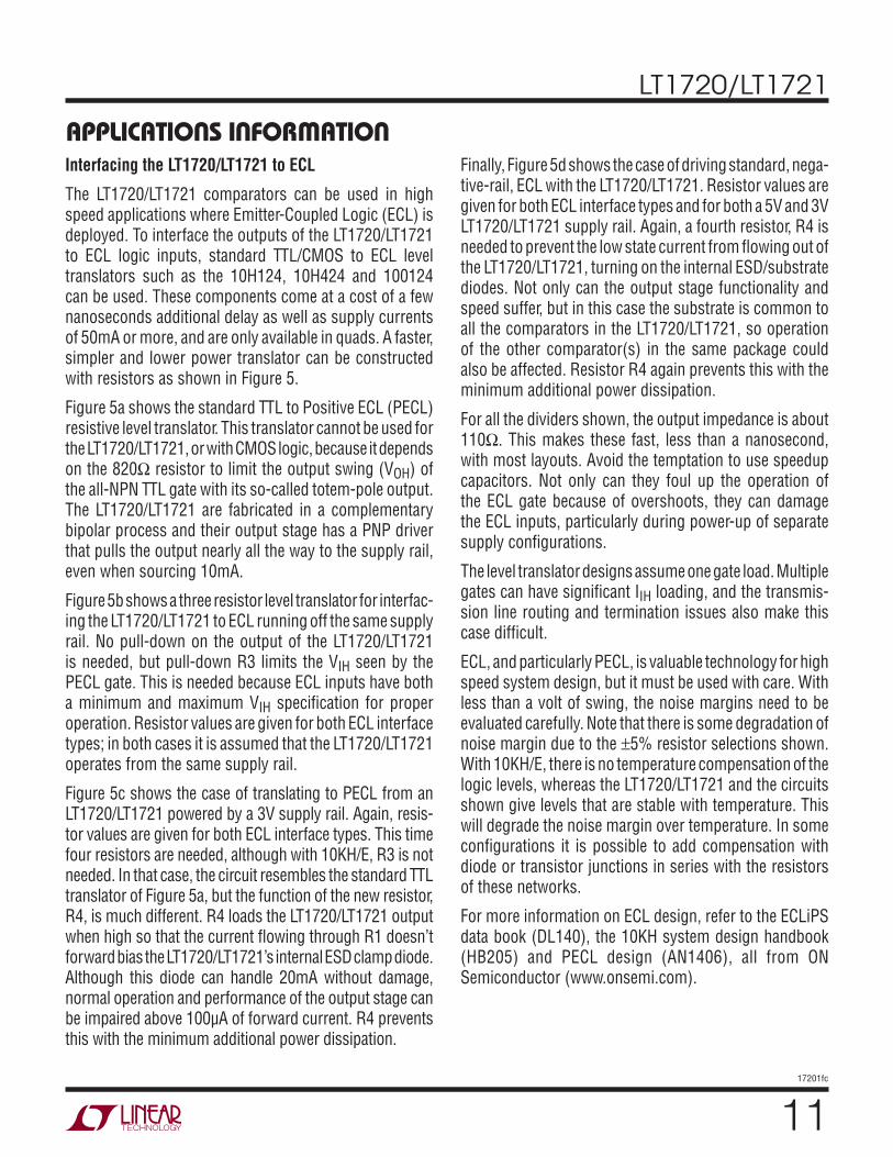
The second step is to recalculate R2 to set the same av-erage threshold as before. The average threshold before was set at VTH = (VREF)(R1)/(R1 + R2). The new R2 is calculated based on the average output voltage (VCC/2) and the simplifi ed circuit model in Figure 4. To assure that the comparator’s noninverting input is, on average, the same VTH as before:
R2′ = (VREF – VTH)/(VTH/R1 + (VTH – VCC/2)/R3)
For additional hysteresis of 10mV or less, it is not uncommon for R2′ to be the same as R2 within 1% resistor tolerances.
This method will work for additional hysteresis of up to a few hundred millivolts. Beyond that, the impedance of R3 is low enough to effect the bias string, and adjust-ment of R1 may also be required. Note that the currents through the R1/R2 bias string should be many times the input currents of the LT1720/LT1721. For 5% accuracy, the current must be at least 120μA(6μA IB ÷ 0.05); more for higher accuracy.
Figure 3. Additional External Hysteresis
–
+
1/2 LT1720
INPUT 17201 F03
R2
VREFR3
R1
Figure 4. Model for Additional Hysteresis Calculations
–
+
1/2 LT1720
17201 F04
R2
VREF
VTH R3 VCC
2VAVERAGE =
R1
LT1720/LT1721
1117201fc
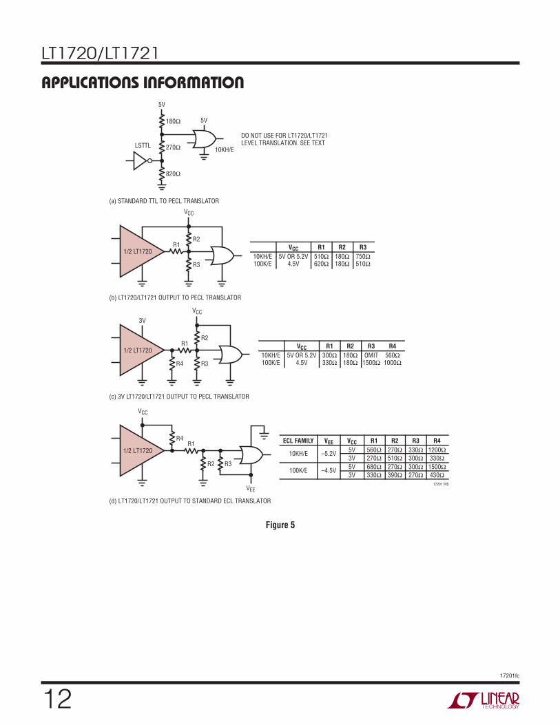
Interfacing the LT1720/LT1721 to ECL
The LT1720/LT1721 comparators can be used in high speed applications where Emitter-Coupled Logic (ECL) is deployed. To interface the outputs of the LT1720/LT1721 to ECL logic inputs, standard TTL/CMOS to ECL level translators such as the 10H124, 10H424 and 100124 can be used. These components come at a cost of a few nanoseconds additional delay as well as supply currents of 50mA or more, and are only available in quads. A faster, simpler and lower power translator can be constructed with resistors as shown in Figure 5.
Figure 5a shows the standard TTL to Positive ECL (PECL) resistive level translator. This translator cannot be used for the LT1720/LT1721, or with CMOS logic, because it depends on the 820Ω resistor to limit the output swing (VOH) of the all-NPN TTL gate with its so-called totem-pole output. The LT1720/LT1721 are fabricated in a complementary bipolar process and their output stage has a PNP driver that pulls the output nearly all the way to the supply rail, even when sourcing 10mA.
Figure 5b shows a three resistor level translator for interfac-ing the LT1720/LT1721 to ECL running off the same supply rail. No pull-down on the output of the LT1720/LT1721 is needed, but pull-down R3 limits the VIH seen by the PECL gate. This is needed because ECL inputs have both a minimum and maximum VIH specifi cation for proper operation. Resistor values are given for both ECL interface types; in both cases it is assumed that the LT1720/LT1721 operates from the same supply rail.
Figure 5c shows the case of translating to PECL from an LT1720/LT1721 powered by a 3V supply rail. Again, resis-tor values are given for both ECL interface types. This time four resistors are needed, although with 10KH/E, R3 is not needed. In that case, the circuit resembles the standard TTL translator of Figure 5a, but the function of the new resistor, R4, is much different. R4 loads the LT1720/LT1721 output when high so that the current fl owing through R1 doesn’t forward bias the LT1720/LT1721’s internal ESD clamp diode. Although this diode can handle 20mA without damage, normal operation and performance of the output stage can be impaired above 100μA of forward current. R4 prevents this with the minimum additional power dissipation.
APPLICATIONS INFORMATIONFinally, Figure 5d shows the case of driving standard, nega-tive-rail, ECL with the LT1720/LT1721. Resistor values are given for both ECL interface types and for both a 5V and 3V LT1720/LT1721 supply rail. Again, a fourth resistor, R4 is needed to prevent the low state current from fl owing out of the LT1720/LT1721, turning on the internal ESD/substrate diodes. Not only can the output stage functionality and speed suffer, but in this case the substrate is common to all the comparators in the LT1720/LT1721, so operation of the other comparator(s) in the same package could also be affected. Resistor R4 again prevents this with the minimum additional power dissipation.
For all the dividers shown, the output impedance is about 110Ω. This makes these fast, less than a nanosecond, with most layouts. Avoid the temptation to use speedup capacitors. Not only can they foul up the operation of the ECL gate because of overshoots, they can damage the ECL inputs, particularly during power-up of separate supply confi gurations.
The level translator designs assume one gate load. Multiple gates can have signifi cant IIH loading, and the transmis-sion line routing and termination issues also make this case diffi cult.
ECL, and particularly PECL, is valuable technology for high speed system design, but it must be used with care. With less than a volt of swing, the noise margins need to be evaluated carefully. Note that there is some degradation of noise margin due to the ±5% resistor selections shown. With 10KH/E, there is no temperature compensation of the logic levels, whereas the LT1720/LT1721 and the circuits shown give levels that are stable with temperature. This will degrade the noise margin over temperature. In some confi gurations it is possible to add compensation with diode or transistor junctions in series with the resistors of these networks.
For more information on ECL design, refer to the ECLiPS data book (DL140), the 10KH system design handbook (HB205) and PECL design (AN1406), all from ON Semiconductor (www.onsemi.com).
LT1720/LT1721
1217201fc
APPLICATIONS INFORMATION
Figure 5
5V
5V180Ω
270Ω
820Ω
10KH/E
R2
VCC
R3
R1
10KH/E100K/E
VCC
5V OR 5.2V4.5V
R1
510Ω620Ω
R2
180Ω180Ω
R3
750Ω510Ω
(a) STANDARD TTL TO PECL TRANSLATOR
(b) LT1720/LT1721 OUTPUT TO PECL TRANSLATOR
LSTTL
1/2 LT1720
R2
VCC
3V
R3R4
R1
10KH/E100K/E
VCC
5V OR 5.2V4.5V
R1
300Ω330Ω
R2
180Ω180Ω
R3
OMIT1500Ω
(c) 3V LT1720/LT1721 OUTPUT TO PECL TRANSLATOR
1/2 LT1720R4
560Ω1000Ω
R4
VEE
VCC
R3
17201 F05
R2
R1ECL FAMILY
10KH/E
VEE
–5.2V
R1
560Ω
270Ω
VCC
5V
3V
R2
270Ω
510Ω
R3
330Ω
300Ω
(d) LT1720/LT1721 OUTPUT TO STANDARD ECL TRANSLATOR
1/2 LT1720
R4
1200Ω
330Ω
100K/E –4.5V680Ω
330Ω
5V
3V
270Ω
390Ω
300Ω
270Ω
1500Ω
430Ω
DO NOT USE FOR LT1720/LT1721LEVEL TRANSLATION. SEE TEXT

LT1720/LT1721
1317201fc
Circuit Description
The block diagram of one comparator in the LT1720/LT1721 is shown in Figure 6. There are differential inputs (+IN/–IN), an output (OUT), a single positive supply (VCC) and ground (GND). All comparators are completely independent, shar-ing only the power and ground pins. The circuit topology consists of a differential input stage, a gain stage with hysteresis and a complementary common-emitter output stage. All of the internal signal paths utilize low voltage swings for high speed at low power.
The input stage topology maximizes the input dynamic range available without requiring the power, complex-ity and die area of two complete input stages such as are found in rail-to-rail input comparators. With a 2.7V supply, the LT1720/LT1721 still have a respectable 1.6V of input common mode range. The differential input volt-age range is rail-to-rail, without the large input currents found in competing devices. The input stage also features phase reversal protection to prevent false outputs when the inputs are driven below the –100mV common mode voltage limit.
The internal hysteresis is implemented by positive, nonlin-ear feedback around a second gain stage. Until this point, the signal path has been entirely differential. The signal path is then split into two drive signals for the upper and lower output transistors. The output transistors are con-nected common emitter for rail-to-rail output operation. The Schottky clamps limit the output voltages at about 300mV from the rail, not quite the 50mV or 15mV of Linear
APPLICATIONS INFORMATIONTechnology’s rail-to-rail amplifiers and other products. But the output of a comparator is digital, and this output stage can drive TTL or CMOS directly. It can also drive ECL, as described earlier, or analog loads as demonstrated in the applications to follow.
The bias conditions and signal swings in the output stages are designed to turn their respective output transistors off faster than on. This nearly eliminates the surge of current from VCC to ground that occurs at transitions, keeping the power consumption low even with high output-toggle frequencies.
The low surge current is what keeps the power consump-tion low at high output-toggle frequencies. The frequency dependence of the supply current is shown in the Typical Performance Characteristics. Just 20pF of capacitive load on the output more than triples the frequency dependent rise. The slope of the no-load curve is just 32μA/MHz. With a 5V supply, this current is the equivalent of charging and discharging just 6.5pF. The slope of the 20pF load curve is 133μA/MHz, an addition of 101μA/MHz, or 20μA/MHz-V, units that are equivalent to picoFarads.
The LT1720/LT1721 dynamic current can be estimated by adding the external capacitive loading to an internal equivalent capacitance of 5pF to 15pF, multiplied by the toggle frequency and the supply voltage. Because the capacitance of routing traces can easily approach these values, the dynamic current is dominated by the load in most circuits.
Figure 6. LT1720/LT1721 Block Diagram
–
+
–
+
–
+
–
+
+IN
–IN
AV1 AV2
NONLINEAR STAGE
OUT
GND17201 F06
VCC
+
+

LT1720/LT1721
1417201fc
Speed Limits
The LT1720/LT1721 comparators are intended for high speed applications, where it is important to understand a few limitations. These limitations can roughly be divided into three categories: input speed limits, output speed limits, and internal speed limits.
There are no significant input speed limits except the shunt capacitance of the input nodes. If the 2pF typical input nodes are driven, the LT1720/LT1721 will respond.
The output speed is constrained by two mechanisms, the fi rst of which is the slew currents available from the output transistors. To maintain low power quiescent op-eration, the LT1720/LT1721 output transistors are sized to deliver 25mA to 45mA typical slew currents. This is sufficient to drive small capacitive loads and logic gate inputs at extremely high speeds. But the slew rate will slow dramatically with heavy capacitive loads. Because the propagation delay (tPD) definition ends at the time the output voltage is halfway between the supplies, the fixed slew current actually makes the LT1720/LT1721 faster at 3V than 5V with 20mV of input overdrive.
Another manifestation of this output speed limit is skew, the difference between tPDLH and tPDHL. The slew currents of the LT1720/LT1721 vary with the process variations of the PNP and NPN transistors, for rising edges and falling edges respectively. The typical 0.5ns skew can have either polarity, rising edge or falling edge faster. Again, the skew will increase dramatically with heavy capacitive loads.
The skews of comparators in a single package are corre-lated, but not identical. Besides some random variability, there is a small (100ps to 200ps) systematic skew due to physical parasitics of the packages. For the LT1720 SO-8, comparator A, whose output is adjacent to the VCC pin, will have a relatively faster rising edge than comparator B. Likewise, comparator B, by virtue of an output adjacent to the ground pin will have a relatively faster falling edge. Similar dependencies occur in the LT1721 S16, while the systemic skews in the smaller MSOP and SSOP packages are half again as small. Of course, if the capacitive loads on the two comparators of a single package are not identical, the differential timing will degrade further.
APPLICATIONS INFORMATIONThe second output speed limit is the clamp turnaround. The LT1720/LT1721 output is optimized for fast initial response, with some loss of turnaround speed, limiting the toggle frequency. The output transistors are idled in a low power state once VOH or VOL is reached by detecting the Schottky clamp action. It is only when the output has slewed from the old voltage to the new voltage, and the clamp circuitry has settled, that the idle state is reached and the output is fully ready to transition again. This clamp turnaround time is typically 8ns for each direction, resulting in a maximum toggle frequency of 62.5MHz, or a 125MB data rate. With higher frequencies, dropout and runt pulses can occur. Increases in capacitive load will increase the time needed for slewing due to the limited slew currents and the maximum toggle frequency will decrease further. For higher toggle frequency applications, refer to the LT1715, whose output stage can toggle at 150MHz typical.
The internal speed limits manifest themselves as disper-sion. All comparators have some degree of dispersion, defined as a change in propagation delay versus input overdrive. The propagation delay of the LT1720/LT1721 will vary with overdrive, from a typical of 4.5ns at 20mV overdrive to 7ns at 5mV overdrive (typical). The LT1720/LT1721’s primary source of dispersion is the hysteresis stage. As a change of polarity arrives at the gain stage, the positive feedback of the hysteresis stage subtracts from the overdrive available. Only when enough time has elapsed for a signal to propagate forward through the gain stage, backwards through the hysteresis stage and forward through the gain stage again, will the output stage receive the same level of overdrive that it would have received in the absence of hysteresis.
With 5mV of overdrive, the LT1720/LT1721 are faster with a 5V supply than with a 3V supply, the opposite of what is true with 20mV overdrive. This is due to the internal speed limit, because the gain stage is faster at 5V than 3V due primarily to the reduced junction capacitances with higher reverse voltage bias.
In many applications, as shown in the following examples, there is plenty of input overdrive. Even in applications providing low levels of overdrive, the LT1720/LT1721 are fast enough that the absolute dispersion of 2.5ns (= 7 – 4.5) is often small enough to ignore.

LT1720/LT1721
1517201fc
The gain and hysteresis stage of the LT1720/LT1721 is simple, short and high speed to help prevent parasitic oscillations while adding minimum dispersion. This internal “self-latch” can be usefully exploited in many applications because it occurs early in the signal chain, in a low power, fully differential stage. It is therefore highly immune to disturbances from other parts of the circuit, either in the same comparator, on the supply lines, or from the other comparator(s) in the same package. Once a high speed signal trips the hysteresis, the output will respond, after a fixed propagation delay, without regard to these external influences that can cause trouble in nonhysteretic comparators.
±VTRIP Test Circuit
The input trip points are tested using the circuit shown in the Test Circuits section that precedes this Applications Information section. The test circuit uses a 1kHz triangle wave to repeatedly trip the comparator being tested. The LT1720/LT1721 output is used to trigger switched capaci-tor sampling of the triangle wave, with a sampler for each direction. Because the triangle wave is attenuated 1000:1 and fed to the LT1720/LT1721’s differential input, the sampled voltages are therefore 1000 times the input trip voltages. The hysteresis and offset are computed from the trip points as shown.
Crystal Oscillators
A simple crystal oscillator using one comparator of an LT1720/LT1721 is shown on the fi rst page of this data sheet. The 2k-620Ω resistor pair set a bias point at the comparator’s noninverting input. The 2k-1.8k-0.1μF path sets the inverting input node at an appropriate DC aver-age level based on the output. The crystal’s path provides resonant positive feedback and stable oscillation occurs. Although the LT1720/LT1721 will give the correct logic output when one input is outside the common mode range, additional delays may occur when it is so operated, open-ing the possibility of spurious operating modes. Therefore, the DC bias voltages at the inputs are set near the center of the LT1720/LT1721’s common mode range and the 220Ω resistor attenuates the feedback to the noninvert-ing input. The circuit will operate with any AT-cut crystal from 1MHz to 10MHz over a 2.7V to 6V supply range.
APPLICATIONS INFORMATIONAs the power is applied, the circuit remains off until the LT1720/LT1721 bias circuits activate, at a typical VCC of 2V to 2.2V (25°C), at which point the desired frequency output is generated.
The output duty cycle for this circuit is roughly 50%, but it is affected by resistor tolerances and, to a lesser extent, by comparator offsets and timings. If a 50% duty cycle is required, the circuit of Figure 7 creates a pair of comple-mentary outputs with a forced 50% duty cycle. Crystals are narrow-band elements, so the feedback to the noninverting input is a filtered analog version of the square wave output. Changing the noninverting reference level can therefore vary the duty cycle. C1 operates as in the previous example, whereas C2 creates a complementary output by compar-ing the same two nodes with the opposite input polarity. A1 compares band-limited versions of the outputs and biases C1’s negative input. C1’s only degree of freedom to respond is variation of pulse width; hence the outputs are forced to 50% duty cycle. Again, the circuit operates from 2.7V to 6V, and the skew between the edges of the two outputs are shown in Figure 8. There is a slight duty cycle dependence on comparator loading, so equal capacitive and resistive loading should be used in critical applications. This circuit works well because of the two matched delays and rail-to-rail style outputs of the LT1720.
Figure 7. Crystal Oscillator with Complementary Outputs and 50% Duty Cycle
–
+
–
+
–
+
C11/2 LT1720
C21/2 LT1720
A1LT1636
VCC2.7V TO 6V
2k
620Ω
220Ω
1MHz TO 10MHzCRYSTAL (AT-CUT)
100k
100k
17201 F07
1.8k
2k
1k
0.1μF
0.1μF
0.1μF
OUTPUT
OUTPUT
GROUNDCASE

LT1720/LT1721
1617201fc
The circuit in Figure 9 shows a crystal oscillator circuit that generates two nonoverlapping clocks by making full use of the two independent comparators of the LT1720. C1 oscillates as before, but with a lower reference level, C2’s output will toggle at different times. The resistors set the degree of separation between the output’s high pulses. With the values shown, each output has a 44% high and 56% low duty cycle, sufficient to allow 2ns between the high pulses. Figure 10 shows the two outputs.
APPLICATIONS INFORMATIONThe optional A1 feedback network shown can be used to force identical output duty cycles. The steady state duty cycles of both outputs will be 44%. Note, though, that the addition of this network only adjusts the percentage of time each output is high to be the same, which can be important in switching circuits requiring identical settling times. It cannot adjust the relative phases between the two outputs to be exactly 180° apart, because the signal at the input node driven by the crystal is not a pure sinusoid.
Figure 8. Timing Skew of Figure 7’s Circuit
SUPPLY VOLTAGE (V)
2.5
OU
TP
UT S
KEW
(ps)
4.5 6.0
1000
800
600
400
200
0
1720/21 F08
3.5 5.53.0 4.0 5.0
Figure 10. Nonoverlapping Outputs of Figure 9’s Circuit
Figure 9. Crystal-Based Nonoverlapping 10MHz Clock Generator
–
+
–
+
–
+
C11/2 LT1720
C21/2 LT1720
A1LT1636
VCC2.7V TO 6V
2k
620Ω
220Ω
10MHzCRYSTAL (AT-CUT)
100k
100k
2.2k
1.3k
2k
1k
17201 F09
0.1μF
0.1μF
0.1μF
OUTPUT 0
OUTPUT 1
GROUNDCASE
OPTIONAL—SEE TEXT
20ns/DIV
Q12V/DIV
Q02V/DIV
17201 F10
LT1720/LT1721
1717201fc
Timing Skews
For a number of reasons, the LT1720/LT1721’s superior timing specifi cations make them an excellent choice for applications requiring accurate differential timing skew. The comparators in a single package are inherently well matched, with just 300ps ΔtPD typical. Monolithic construc-tion keeps the delays well matched vs supply voltage and temperature. Crosstalk between the comparators, usually a disadvantage in monolithic duals and quads, has minimal effect on the LT1720/LT1721 timing due to the internal hysteresis, as described in the Speed Limits section.
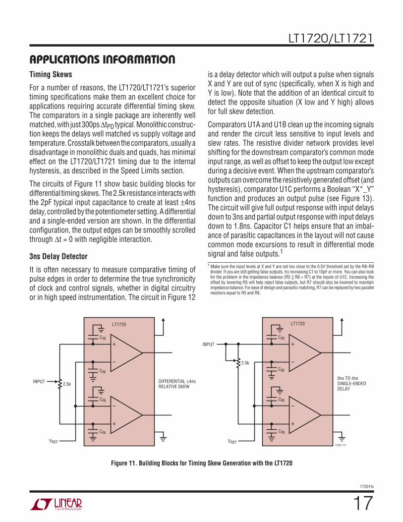
The circuits of Figure 11 show basic building blocks for differential timing skews. The 2.5k resistance interacts with the 2pF typical input capacitance to create at least ±4ns delay, controlled by the potentiometer setting. A differential and a single-ended version are shown. In the differential configuration, the output edges can be smoothly scrolled through Δt = 0 with negligible interaction.
3ns Delay Detector
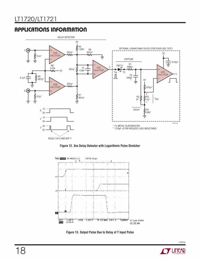
It is often necessary to measure comparative timing of pulse edges in order to determine the true synchronicity of clock and control signals, whether in digital circuitry or in high speed instrumentation. The circuit in Figure 12
APPLICATIONS INFORMATIONis a delay detector which will output a pulse when signals X and Y are out of sync (specifi cally, when X is high and Y is low). Note that the addition of an identical circuit to detect the opposite situation (X low and Y high) allows for full skew detection.
Comparators U1A and U1B clean up the incoming signals and render the circuit less sensitive to input levels and slew rates. The resistive divider network provides level shifting for the downstream comparator’s common mode input range, as well as offset to keep the output low except during a decisive event. When the upstream comparator’s outputs can overcome the resistively generated offset (and hysteresis), comparator U1C performs a Boolean “X*_Y” function and produces an output pulse (see Figure 13). The circuit will give full output response with input delays down to 3ns and partial output response with input delays down to 1.8ns. Capacitor C1 helps ensure that an imbal-ance of parasitic capacitances in the layout will not cause common mode excursions to result in differential mode signal and false outputs.1
1 Make sure the input levels at X and Y are not too close to the 0.5V threshold set by the R8–R9 divider. If you are still getting false outputs, try increasing C1 to 10pF or more. You can also look for the problem in the impedance balance (R5 || R6 = R7) at the inputs of U1C. Increasing the offset by lowering R5 will help reject false outputs, but R7 should also be lowered to maintain impedance balance. For ease of design and parasitic matching, R7 can be replaced by two parallel resistors equal to R5 and R6.
LT1720
DIFFERENTIAL 4nsRELATIVE SKEW
CIN
CIN
CIN
CIN
VREF
2.5k
2.5k
INPUT
LT1720
0ns TO 4ns SINGLE-ENDEDDELAY
CIN
CIN
17201 F11
VREF
INPUT
CIN
CIN–
+
–
+
–
+
–
+
Figure 11. Building Blocks for Timing Skew Generation with the LT1720
LT1720/LT1721
1817201fc
APPLICATIONS INFORMATION
Figure 12. 3ns Delay Detector with Logarithmic Pulse Stretcher
5V
–
+U1A
1/4 LT1721
Y
51Ω*
R8*4.53k
5V
5V
17201 F12
0.1μF
C15.6pF
0.33μF
R9487Ω*
+
–U1B
1/4 LT1721
+
–U1C
1/4 LT1721
X
1VX
0V
51Ω*
C2540pF
**
R7261Ω*
Z
–
+U1D
1/4 LT1721
301Ω*
R51.82k* R6
301Ω*
5V
R430Ω*
R31Ω* VOFF
R21k*
475Ω*
L
301Ω*
301Ω*
RESULT OF X AND NOT Y
+
–
R1499Ω*
DECAY
CAPTURE
OPTIONAL LOGARITHMIC PULSE STRETCHER (SEE TEXT)
VCVIN
1N5711
DELAY DETECTOR
1VY
0V
5VZ
0V
* 1% METAL FILM RESISTOR** 270pF 2 FOR REDUCED LEAD INDUCTANCE
Figure 13. Output Pulse Due to Delay of Y Input Pulse

LT1720/LT1721
1917201fc
Optional Logarithmic Pulse Stretcher
The fourth comparator of the quad LT1721 can be put to work as a logarithmic pulse stretcher. This simple circuit can help tremendously if you don’t have a fast enough oscilloscope (or control circuit) to easily capture 3ns pulse widths (or faster). When an input pulse occurs, C2 is charged up with a 180ns capture2 time constant. The hysteresis and 10mV offset across R3 are overcome within the fi rst nanosecond3, switching the comparator output high. When the input pulse subsides, C2 discharges with a 540ns time constant, keeping the comparator on until the decay overrides the 10mV offset across R3 minus hysteresis. Because of this exponential decay, the output pulse width will be proportional to the logarithm of the input pulse width. It is important to bypass the circuit’s VCC well to avoid coupling into the resistive divider. R4 keeps the quiescent input voltage in a range where forward leakage of the diode due to the 0.4V VOL of the driving comparator is not a problem.
Neglecting some effects4, the output pulse is related to the input pulse as:
tOUT = τ2 • ln {VCH • [1 – exp (–tP/τ1)]/(VOFF – VH/2)}
– τ1 • ln [VCH/(VCH – VOFF – VH/2)]
+ tP (1)
where
tP = input pulse width
tOUT = output pulse width
τ1 = R1 || R2 • C2 the capture time constant
τ2 = R2 • C2 the decay time constant
VOFF = 10mV the voltage drop across R1
VH = 3.5mV LT1721 hysteresis
VC = VIN – VFDIODE the input pulse voltage after the diode drop
VCH = VC • R2/(R1 + R2) the effective source voltage for the charge
APPLICATIONS INFORMATIONFor simplicity, with tP < τ1, and neglecting the very slight delay in turn-on due to offset and hysteresis, the equation can be approximated by:
tOUT = τ2 • ln [(VCH • tP/τ1)/(VOFF – VH/2)] (2)
For example, an 8ns input pulse gives a 1.67μs output pulse. Doubling the input pulse to 16ns lengthens the output pulse by 0.37μs. Doubling the input pulse again to 32ns adds another 0.37μs to the output pulse, and so on. The rate of 0.37μs per octave falls out of the above equation as:
ΔtOUT/octave = τ2 • ln(2) (3)
There is ±0.01μs jitter5 in the output pulse which gives an uncertainty referred to the input pulse of less than 2% (60ps resolution on a 3ns pulse with a 60MHz oscilloscope—not bad!). The beauty of this circuit is that it gives resolution precisely where it’s hardest to get. The jitter is due to a combination of the slow decay of the last few millivolts on C2 and the 4nV/√Hz noise and 400MHz bandwidth of the LT1721 input stage. Increasing the offset across R3 or decreasing τ2 will decrease this jitter at the expense of dynamic range.
The circuit topology itself is extremely fast, limited theo-retically only by the speed of the diode, the capture time constant τ1 and the pulse source impedance. Figure 14 shows results achieved with the implementation shown, compared to a plot of Equation (1). The low end is limited by the delivery time of the upstream comparators. As the input pulse width is increased, the log function is con-strained by the asymptotic RC response but, rather than becoming clamped, becomes time linear. Thus, for very long input pulses the third term of Equation (1) dominates and the circuit becomes a 3μs pulse stretcher.
2 So called because the very fast input pulse is “captured,” for later examination, as a charge on the capacitor.
3 Assuming the input pulse slew rate at the diode is infi nite. This effective delay constant, about 0.4% of τ1 or 0.8ns, is the second term of equation 1, below. Driven by the 2.5ns slew-limited LT1721, this effective delay will be 2ns.
4 VC is dependent on the LT1721 output voltage and nonlinear diode characteristics. Also, the Thevenin equivalent charge voltage seen by C2 is boosted slightly by R2 being terminated above ground.
5 Output jitter increases with inputs pulse widths below ~3ns.

LT1720/LT1721
2017201fc
You don’t need expensive equipment to confi rm the actual overall performance of this circuit. All you need is a respect-able waveform generator (capable of >~100kHz), a splitter, a variety of cable lengths and a 20MHz or 60MHz oscilloscope. Split a single pulse source into different cable lengths and then into the delay detector, feeding the longer cable into the Y input (see Figure 15). A 6 foot cable length difference will create a ~9.2ns delay (using 66% propagation speed RG-58 cable), and should result in easily measured 1.70μs output pulses. A 12 foot cable length difference will result in ~18.4ns delay and 2.07μs output pulses. The difference
APPLICATIONS INFORMATIONin the two output pulse widths is the per-octave response of your circuit (see Equation (3)). Shorter cable length dif-ferences can be used to get a plot of circuit performance down to 1.5ns (if any), which can then later be used as a lookup reference when you have moved from quantifying the circuit to using the circuit. (Note there is a slight aberration in performance below 10ns. See Figure 14.) As a fi nal check, feed the circuit with identical cable lengths and check that it is not producing any output pulses.
10ns Triple Overlap Generator
The circuit of Figure 16 utilizes an LT1721 to generate three overlapping outputs whose pulse edges are separated by 10ns as shown. The time constant is set by the RC net-work on the output of comparator A. Comparator B and D trip at fi xed percentages of the exponential voltage decay across the capacitor. The 4.22kΩ feed-forward to the C comparator’s inverting input keeps the delay differences the same in each direction despite the exponential nature of the RC network’s voltage.
There is a 15ns delay to the fi rst edge in both directions, due to the 4.5ns delay of two LT1721 comparators, plus 6ns delay in the RC network. This starting delay is shortened somewhat if the pulse was shorter than 40ns because the RC network will not have fully settled; however, the 10ns edge separations stay constant.
The values shown utilize only the lowest 75% of the supply voltage span, which allows it to work down to 2.7V supply. The delay differences grow a couple nanoseconds from 5V to 2.7V supply due to the fi xed VOL/VOH drops which grow as a percentage at low supply voltage. To keep this effect to a minimum, the 1kΩ pull-up on comparator A provides equal loading in either state.
Fast Waveform Sampler
Figure 17 uses a diode-bridge-type switch for clean, fast waveform sampling. The diode bridge, because of its inherent symmetry, provides lower AC errors than other semiconductor-based switching technologies. This circuit features 20dB of gain, 10MHz full power bandwidth and 100μV/°C baseline uncertainty. Switching delay is less than 15ns and the minimum sampling window width for full power response is 30ns.
Figure 14. Log Pulse Stretcher Output Pulse vs Input Pulse
tPULSE (ns)
t OU
T S
TR
ETC
HED
(μs)
14
12
10
8
6
4
2
01 100 1000 10000
17201 F14
10
MEASURED
EQUATION 1
Figure 15. RG-58 Cable with Velocity of Propogation = 66%;Delay at Y = (n – 1) • 1.54ns
SPLITTER2V
0V
CIRCUIT OFFIGURE 12
n FOOT CABLE
1 FOOT CABLE
NANOSECONDINPUT RANGE
MICROSECONDOUTPUT RANGE
X
Y
L
tOUT
(SEE TEXT)
17201 F15

LT1720/LT1721
2117201fc
APPLICATIONS INFORMATION
Figure 16. 10ns Triple Overlap Generator
VCC
–
+U1A
1/4 LT1721
–
+U1B
1/4 LT1721
–
+U1D
1/4 LT1721
–
+U1C
1/4 LT1721681Ω
681Ω
1.37k
VCC
909Ω
215Ω
VCC
INPUT
OUTPUTS
VREF 100pF
453Ω
1k
750Ω
VCC
10ns 10ns
10ns
17201 F16
10ns
4.22k
Figure 17. Fast Waveform Sampler Using the LT1720 for Timing-Skew Compensation
–
+
5V
2.2k 2.2k
INPUT100mV FULL SCALE
1k LT1227
909Ω
100Ω
OUTPUT1V FULL SCALE
5V
AC BALANCE
3pF
3.6k1.5k
0.1μF
CIN
CIN
2k
2k
10pF
SKEWCOMP
2.5k
1.1k
1.1k 1.1k
1.1k
820Ω 820Ω
MRF501 MRF501
LM3045
11
9 6
8
DC BALANCE
500Ω
51Ω 51Ω
10 7
680Ω
–5V
17201 F17
13
= 1N5711
= CA3039 DIODE ARRAY (SUBSTRATE TO –5V)
–
+
1/2 LT1720
–
+
1/2 LT1720
SAMPLECOMMAND
LT1720/LT1721
2217201fc
The input waveform is presented to the diode bridge switch, the output of which feeds the LT1227 wideband amplifier. The LT1720 comparators, triggered by the sample com-mand, generate phase-opposed outputs. These signals are level shifted by the transistors, providing complementary bipolar drive to switch the bridge. A skew compensation trim ensures bridge-drive signal simultaneity within 1ns. The AC balance corrects for parasitic capacitive bridge im-balances. A DC balance adjustment trims bridge offset.
The trim sequence involves grounding the input via 50Ω and applying a 100kHz sample command. The DC balance is adjusted for minimal bridge ON vs OFF variation at the output. The skew compensation and AC
APPLICATIONS INFORMATIONbalance adjustments are then optimized for minimum AC disturbance in the output. Finally, unground the input and the circuit is ready for use.
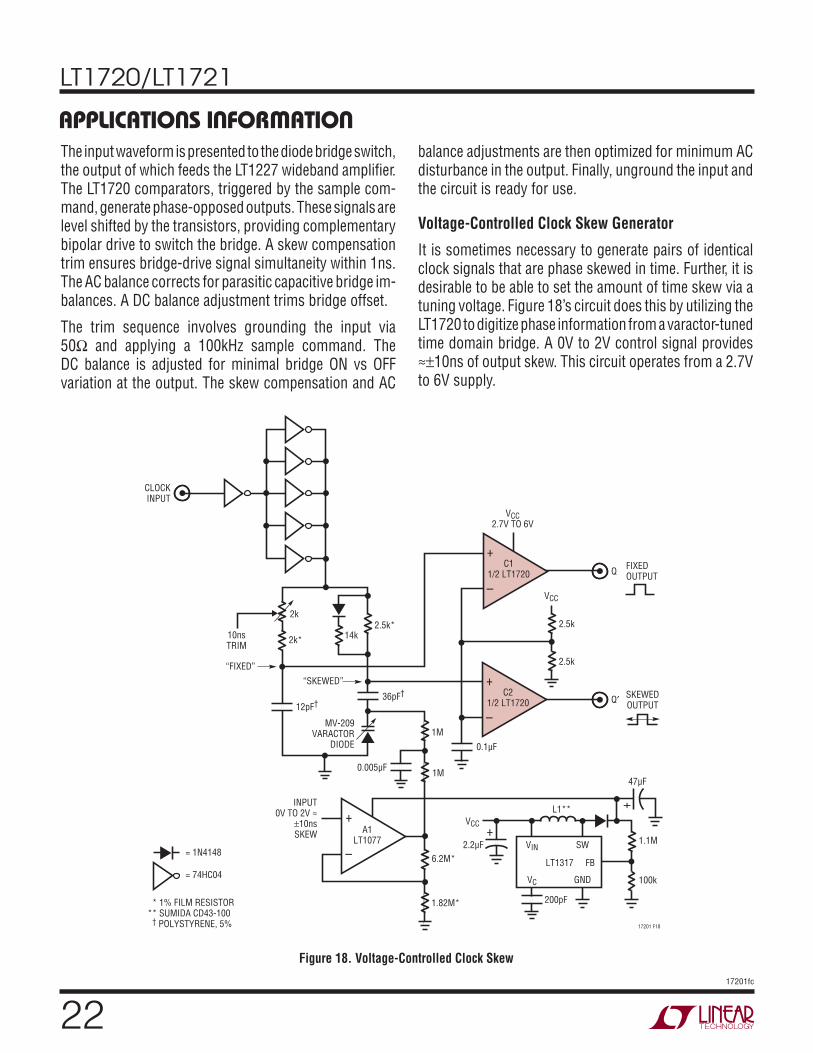
Voltage-Controlled Clock Skew Generator
It is sometimes necessary to generate pairs of identical clock signals that are phase skewed in time. Further, it is desirable to be able to set the amount of time skew via a tuning voltage. Figure 18’s circuit does this by utilizing the LT1720 to digitize phase information from a varactor-tuned time domain bridge. A 0V to 2V control signal provides ≈±10ns of output skew. This circuit operates from a 2.7V to 6V supply.
Figure 18. Voltage-Controlled Clock Skew
17201 F18
–
+C2
1/2 LT1720
VCC2.7V TO 6V
VCC
Q
Q
FIXEDOUTPUT
MV-209VARACTOR
DIODE
2.5k
CLOCKINPUT
2.5k
0.1μF
2.2μF
0.005μF
“SKEWED”
“FIXED”
10nsTRIM
36pF†
1.82M*
6.2M*
1.1M
100k
200pF
2k*
–
+C1
1/2 LT1720
SKEWEDOUTPUT
INPUT0V TO 2V ≈
10nsSKEW
2.5k*14k
2k
12pF†
1M
1M
VCC
–
+A1
LT1077
* 1% FILM RESISTOR** SUMIDA CD43-100
† POLYSTYRENE, 5%
= 1N4148
= 74HC04
+
LT1317
VIN SW
47μF
L1**
VC GND
FB
+
LT1720/LT1721
2317201fc
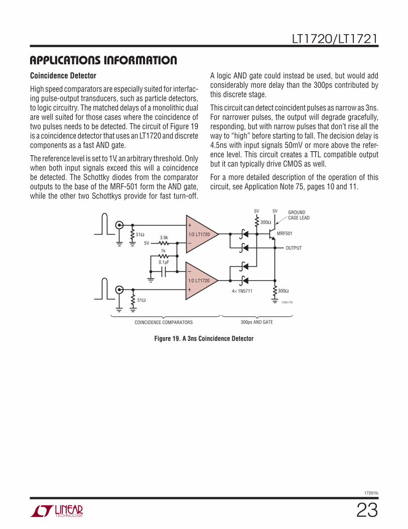
APPLICATIONS INFORMATIONCoincidence Detector
High speed comparators are especially suited for interfac-ing pulse-output transducers, such as particle detectors, to logic circuitry. The matched delays of a monolithic dual are well suited for those cases where the coincidence of two pulses needs to be detected. The circuit of Figure 19 is a coincidence detector that uses an LT1720 and discrete components as a fast AND gate.
The reference level is set to 1V, an arbitrary threshold. Only when both input signals exceed this will a coincidence be detected. The Schottky diodes from the comparator outputs to the base of the MRF-501 form the AND gate, while the other two Schottkys provide for fast turn-off.
A logic AND gate could instead be used, but would add considerably more delay than the 300ps contributed by this discrete stage.
This circuit can detect coincident pulses as narrow as 3ns. For narrower pulses, the output will degrade gracefully, responding, but with narrow pulses that don’t rise all the way to “high” before starting to fall. The decision delay is 4.5ns with input signals 50mV or more above the refer-ence level. This circuit creates a TTL compatible output but it can typically drive CMOS as well.
For a more detailed description of the operation of this circuit, see Application Note 75, pages 10 and 11.
Figure 19. A 3ns Coincidence Detector
5V3.9k
1k
0.1μF
51Ω
51Ω
300Ω
300Ω
5V 5V
4 1N5711
MRF501
OUTPUT
GROUNDCASE LEAD
COINCIDENCE COMPARATORS 300ps AND GATE
17201 F19
1/2 LT1720
–
+
–
+1/2 LT1720
LT1720/LT1721
2417201fc
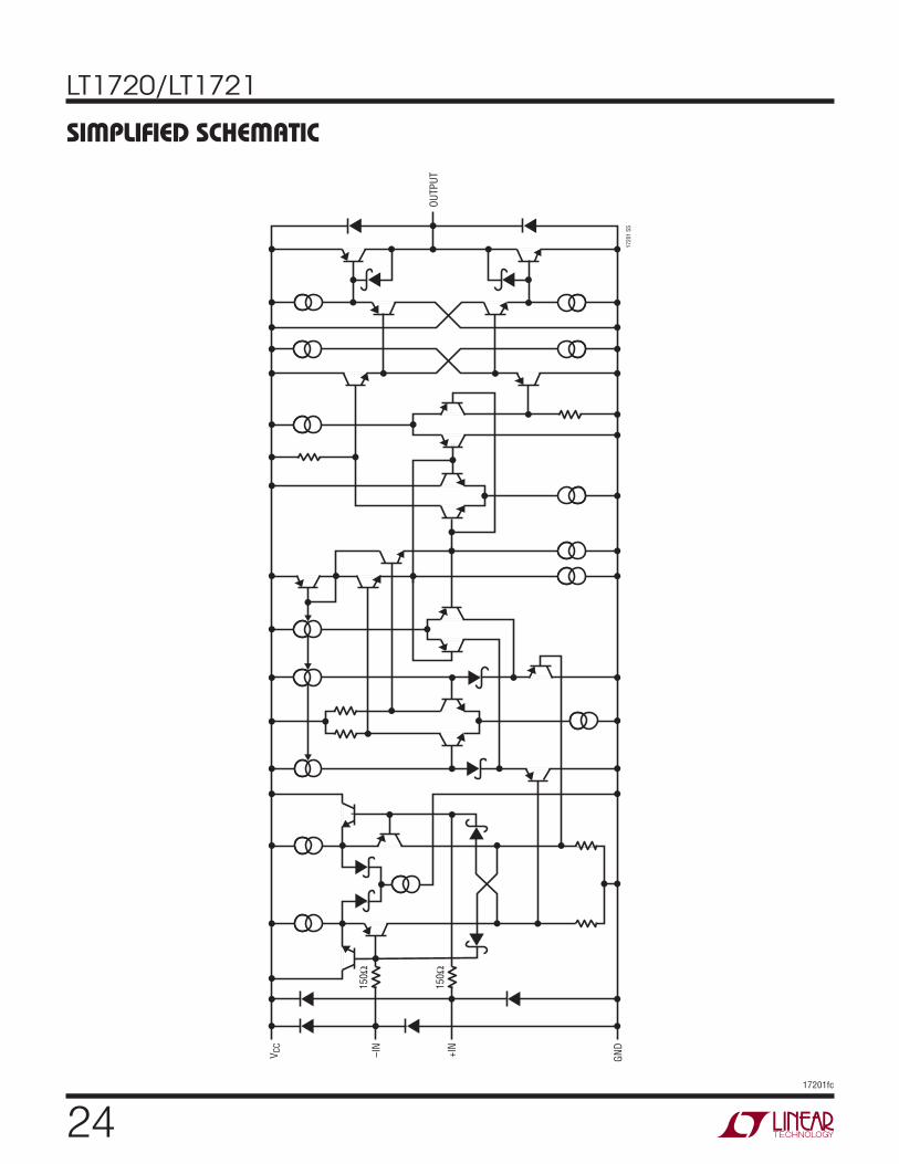
SIMPLIFIED SCHEMATIC
–IN
+IN
GN
D1
72
01
SS
OU
TP
UT
VC
C
150Ω
150Ω
LT1720/LT1721
2517201fc
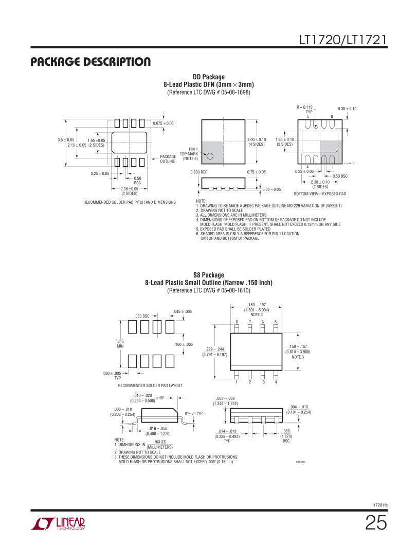
PACKAGE DESCRIPTIONDD Package
8-Lead Plastic DFN (3mm × 3mm)(Reference LTC DWG # 05-08-1698)
3.00 0.10(4 SIDES)
NOTE:1. DRAWING TO BE MADE A JEDEC PACKAGE OUTLINE M0-229 VARIATION OF (WEED-1)2. DRAWING NOT TO SCALE3. ALL DIMENSIONS ARE IN MILLIMETERS4. DIMENSIONS OF EXPOSED PAD ON BOTTOM OF PACKAGE DO NOT INCLUDE MOLD FLASH. MOLD FLASH, IF PRESENT, SHALL NOT EXCEED 0.15mm ON ANY SIDE5. EXPOSED PAD SHALL BE SOLDER PLATED6. SHADED AREA IS ONLY A REFERENCE FOR PIN 1 LOCATION ON TOP AND BOTTOM OF PACKAGE
0.38 0.10
BOTTOM VIEW—EXPOSED PAD
1.65 0.10(2 SIDES)
0.75 0.05
R = 0.115TYP
2.38 0.10(2 SIDES)
14
85
PIN 1TOP MARK
(NOTE 6)
0.200 REF
0.00 – 0.05
(DD) DFN 1203
0.25 0.05
2.38 0.05(2 SIDES)
RECOMMENDED SOLDER PAD PITCH AND DIMENSIONS
1.65 0.05(2 SIDES)2.15 0.05
0.50BSC
0.675 0.05
3.5 0.05
PACKAGEOUTLINE
0.25 0.050.50 BSC
S8 Package8-Lead Plastic Small Outline (Narrow .150 Inch)
(Reference LTC DWG # 05-08-1610)
.016 – .050
(0.406 – 1.270)
.010 – .020
(0.254 – 0.508) 45
0 – 8 TYP.008 – .010
(0.203 – 0.254)
SO8 0303
.053 – .069
(1.346 – 1.752)
.014 – .019
(0.355 – 0.483)TYP
.004 – .010
(0.101 – 0.254)
.050
(1.270)BSC
1 2 3 4
.150 – .157
(3.810 – 3.988)
NOTE 3
8 7 6 5
.189 – .197
(4.801 – 5.004)NOTE 3
.228 – .244
(5.791 – 6.197)
.245MIN .160 .005
RECOMMENDED SOLDER PAD LAYOUT
.045 .005.050 BSC
.030 .005 TYP
INCHES
(MILLIMETERS)
NOTE:1. DIMENSIONS IN
2. DRAWING NOT TO SCALE3. THESE DIMENSIONS DO NOT INCLUDE MOLD FLASH OR PROTRUSIONS. MOLD FLASH OR PROTRUSIONS SHALL NOT EXCEED .006" (0.15mm)
LT1720/LT1721
2617201fc
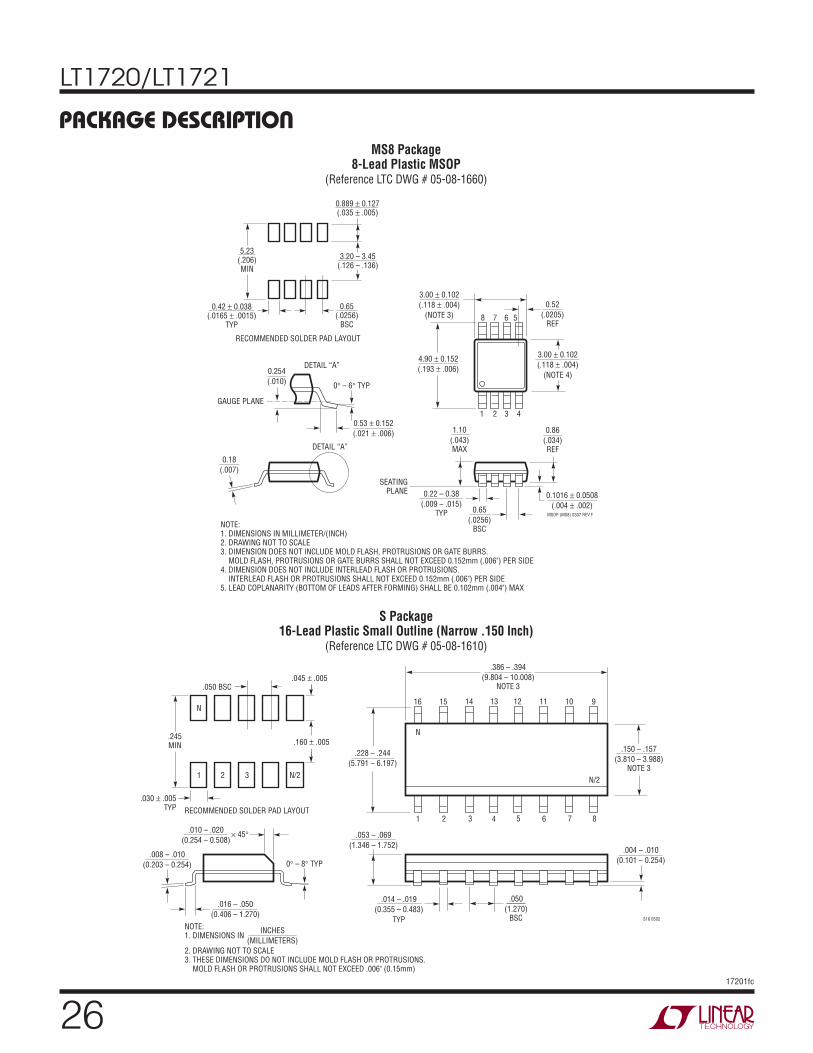
PACKAGE DESCRIPTIONMS8 Package
8-Lead Plastic MSOP(Reference LTC DWG # 05-08-1660)
MSOP (MS8) 0307 REV F
0.53 0.152
(.021 .006)
SEATINGPLANE
NOTE:1. DIMENSIONS IN MILLIMETER/(INCH)2. DRAWING NOT TO SCALE3. DIMENSION DOES NOT INCLUDE MOLD FLASH, PROTRUSIONS OR GATE BURRS. MOLD FLASH, PROTRUSIONS OR GATE BURRS SHALL NOT EXCEED 0.152mm (.006") PER SIDE4. DIMENSION DOES NOT INCLUDE INTERLEAD FLASH OR PROTRUSIONS. INTERLEAD FLASH OR PROTRUSIONS SHALL NOT EXCEED 0.152mm (.006") PER SIDE5. LEAD COPLANARITY (BOTTOM OF LEADS AFTER FORMING) SHALL BE 0.102mm (.004") MAX
0.18
(.007)
0.254
(.010)
1.10
(.043)MAX
0.22 – 0.38
(.009 – .015)TYP
0.1016 0.0508
(.004 .002)
0.86
(.034)REF
0.65
(.0256)BSC
0 – 6 TYP
DETAIL “A”
DETAIL “A”
GAUGE PLANE
1 2 3 4
4.90 0.152
(.193 .006)
8 7 6 5
3.00 0.102
(.118 .004)
(NOTE 3)
3.00 0.102
(.118 .004)
(NOTE 4)
0.52
(.0205)REF
5.23(.206)MIN
3.20 – 3.45(.126 – .136)
0.889 0.127(.035 .005)
RECOMMENDED SOLDER PAD LAYOUT
0.42 0.038(.0165 .0015)
TYP
0.65(.0256)
BSC
S Package16-Lead Plastic Small Outline (Narrow .150 Inch)
(Reference LTC DWG # 05-08-1610)
.016 – .050
(0.406 – 1.270)
.010 – .020
(0.254 – 0.508) 45
0 – 8 TYP.008 – .010
(0.203 – 0.254)
1
N
2 3 4 5 6 7 8
N/2
.150 – .157
(3.810 – 3.988)NOTE 3
16 15 14 13
.386 – .394
(9.804 – 10.008)NOTE 3
.228 – .244
(5.791 – 6.197)
12 11 10 9
S16 0502
.053 – .069
(1.346 – 1.752)
.014 – .019
(0.355 – 0.483)
TYP
.004 – .010
(0.101 – 0.254)
.050
(1.270)BSC
.245MIN
N
1 2 3 N/2
.160 .005
RECOMMENDED SOLDER PAD LAYOUT
.045 .005.050 BSC
.030 .005 TYP
INCHES
(MILLIMETERS)
NOTE:1. DIMENSIONS IN
2. DRAWING NOT TO SCALE3. THESE DIMENSIONS DO NOT INCLUDE MOLD FLASH OR PROTRUSIONS. MOLD FLASH OR PROTRUSIONS SHALL NOT EXCEED .006" (0.15mm)
LT1720/LT1721
2717201fc
Information furnished by Linear Technology Corporation is believed to be accurate and reliable. However, no responsibility is assumed for its use. Linear Technology Corporation makes no representa-tion that the interconnection of its circuits as described herein will not infringe on existing patent rights.
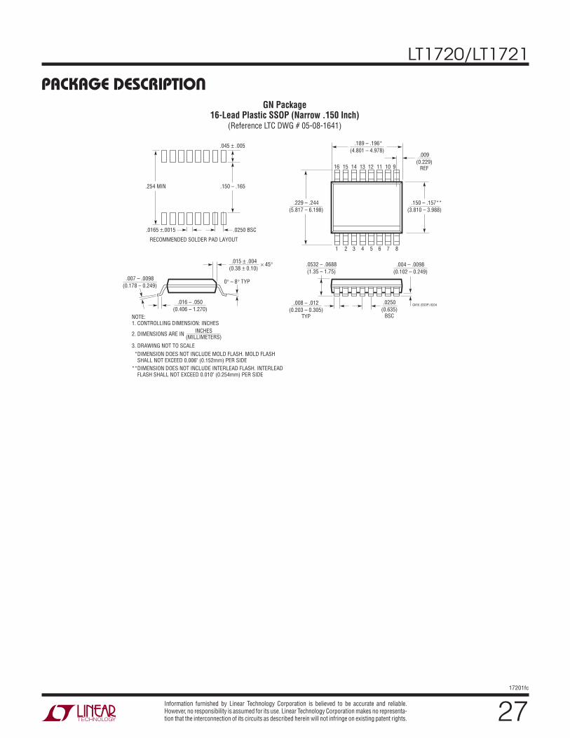
PACKAGE DESCRIPTIONGN Package
16-Lead Plastic SSOP (Narrow .150 Inch)(Reference LTC DWG # 05-08-1641)
GN16 (SSOP) 0204
1 2 3 4 5 6 7 8
.229 – .244
(5.817 – 6.198)
.150 – .157**
(3.810 – 3.988)
16 15 14 13
.189 – .196*
(4.801 – 4.978)
12 11 10 9
.016 – .050
(0.406 – 1.270)
.015 .004
(0.38 0.10) 45
0 – 8 TYP.007 – .0098
(0.178 – 0.249)
.0532 – .0688
(1.35 – 1.75)
.008 – .012
(0.203 – 0.305)TYP
.004 – .0098
(0.102 – 0.249)
.0250
(0.635)BSC
.009
(0.229)REF
.254 MIN
RECOMMENDED SOLDER PAD LAYOUT
.150 – .165
.0250 BSC.0165 .0015
.045 .005
* DIMENSION DOES NOT INCLUDE MOLD FLASH. MOLD FLASH SHALL NOT EXCEED 0.006" (0.152mm) PER SIDE
** DIMENSION DOES NOT INCLUDE INTERLEAD FLASH. INTERLEAD FLASH SHALL NOT EXCEED 0.010" (0.254mm) PER SIDE
INCHES(MILLIMETERS)
NOTE:1. CONTROLLING DIMENSION: INCHES
2. DIMENSIONS ARE IN
3. DRAWING NOT TO SCALE
LT1720/LT1721
2817201fc
Linear Technology Corporation1630 McCarthy Blvd., Milpitas, CA 95035-7417 (408) 432-1900 ● FAX: (408) 434-0507 ● www.linear.com © LINEAR TECHNOLOGY CORPORATION 1998
LT 0908 REV C • PRINTED IN USA
RELATED PARTS
TYPICAL APPLICATION
PART NUMBER DESCRIPTION COMMENTS
LT1016 UltraFast Precision Comparator Industry Standard 10ns Comparator
LT1116 12ns Single Supply Ground-Sensing Comparator Single Supply Version of LT1016
LT1394 7ns, UltraFast, Single Supply Comparator 6mA Single Supply Comparator
LT1671 60ns, Low Power, Single Supply Comparator 450μA Single Supply Comparator
LT1715 4ns, 150MHz Dual Comparator Similar to the LT1720 with Independent Input/Output Supplies
LT1719 4.5ns Single Supply 3V/5V Comparator Single Comparator Similar to the LT1720/LT1721
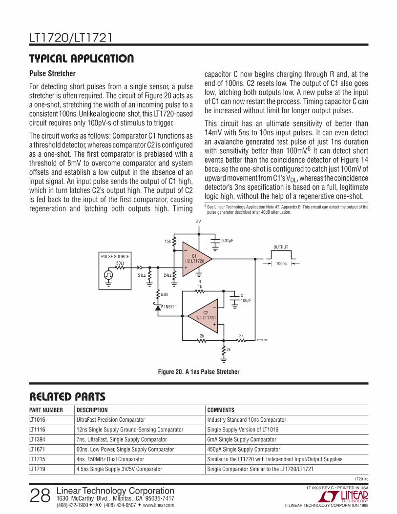
Pulse Stretcher
For detecting short pulses from a single sensor, a pulse stretcher is often required. The circuit of Figure 20 acts as a one-shot, stretching the width of an incoming pulse to a consistent 100ns. Unlike a logic one-shot, this LT1720-based circuit requires only 100pV-s of stimulus to trigger.
The circuit works as follows: Comparator C1 functions as a threshold detector, whereas comparator C2 is configured as a one-shot. The first comparator is prebiased with a threshold of 8mV to overcome comparator and system offsets and establish a low output in the absence of an input signal. An input pulse sends the output of C1 high, which in turn latches C2’s output high. The output of C2 is fed back to the input of the first comparator, causing regeneration and latching both outputs high. Timing
capacitor C now begins charging through R and, at the end of 100ns, C2 resets low. The output of C1 also goes low, latching both outputs low. A new pulse at the input of C1 can now restart the process. Timing capacitor C can be increased without limit for longer output pulses.
This circuit has an ultimate sensitivity of better than 14mV with 5ns to 10ns input pulses. It can even detect an avalanche generated test pulse of just 1ns duration with sensitivity better than 100mV.6 It can detect short events better than the coincidence detector of Figure 14 because the one-shot is configured to catch just 100mV of upward movement from C1’s VOL, whereas the coincidence detector’s 3ns specification is based on a full, legitimate logic high, without the help of a regenerative one-shot.6 See Linear Technology Application Note 47, Appendix B. This circuit can detect the output of the
pulse generator described after 40dB attenuation.
–
+
–
+
PULSE SOURCE C11/2 LT1720
C21/2 LT1720
50Ω
51Ω
6.8k
1N5711
24Ω
15k
R1k
2k 2k17201 F20
2k
C100pF
0.01μF
OUTPUT
100ns
5V
Figure 20. A 1ns Pulse Stretcher