Low-Resistivity Long-Length Horizontal Carbon Nanotube Bundles for Interconnect Applications—Part...
8
2862 IEEE TRANSACTIONS ON ELECTRON DEVICES, VOL. 60, NO. 9, SEPTEMBER 2013 Low-Resistivity Long-Length Horizontal Carbon Nanotube Bundles for Interconnect Applications—Part I: Process Development Hong Li, Member, IEEE , Wei Liu, Member, IEEE, Alan M. Cassell, Franz Kreupl, Member, IEEE, and Kaustav Banerjee, Fellow, IEEE Abstract— Although horizontally-aligned carbon nanotube (HACNT) interconnects are the most common scenarios that have been modeled and analyzed in theoretical research, fab- rication of HACNT test structures has remained an enigma until now. Through addressing several fabrication challenges, this paper reports a novel process that enables fabrication of high- density, long (over hundred microns), and thick (up to microme- ter) HACNT interconnects. Furthermore, horizontal CNT-based 2-D Manhattan structure is demonstrated by properly designing the catalyst and flattening process. These structures are crucial for building angled interconnects and on-chip passive devices. In addition, to address the contact issue between metal and thick HACNT bundles, a multistep lithography combined with specifically designed metal deposition technique is performed to ensure full contact configuration. Using such a process, test structures with arrays of various sizes of HACNT bundle interconnects are fabricated. The process developed in this paper provides an important platform for future research and technology development of CNT-based interconnects and passive elements. Index Terms— Carbon nanotubes (CNTs), chemical vapor deposition, contact, horizontally aligned, interconnects, Manhattan structure, resistivity. I. I NTRODUCTION I NTERCONNECTS in advanced very large scale integrated circuits, based on Cu are confronting an acute problem in terms of performance and reliability because of signifi- cant size effects resulting in a sharp rise in resistivity and degradation in current carrying capacity [1], [2]. Carbon nanotubes (CNTs) have shown promise in many ways, because of their excellent electrical, thermal, and mechanical properties Manuscript received February 8, 2013; revised May 15, 2013; accepted May 19, 2013. Date of current version August 19, 2013. This work was supported by the National Science Foundation under Grant CCF-0811880. The review of this paper was arranged by Editor A. C. Seabaugh. H. Li was with the Department of Electrical and Computer Engineer- ing, University of California, Santa Barbara, CA 93106 USA. He is now with Emerging Memory Group, Micron Technology, Boise, ID 83707 USA (e-mail: [email protected]). W. Liu and K. Banerjee are with the Department of Electrical and Computer Engineering, University of California, Santa Barbara, CA 93106 USA (e-mail: [email protected]; [email protected]). A. M. Cassell is with NASA Ames Research Center, Moffett Field, CA 94035 USA (e-mail: [email protected]). F. Kreupl is with the Department of Hybrid Electronic Systems, Technische Universität München 80333, Germany (e-mail: [email protected]). Color versions of one or more of the figures in this paper are available online at http://ieeexplore.ieee.org. Digital Object Identifier 10.1109/TED.2013.2275259 [3]–[5], to potentially solve the performance and relia- bility requirements of both horizontal and vertical inter- connects for next-generation electronics [6]–[8]. Since the first demonstration of CNT-based vertical interconnects (vias) [9]–[11], research in both theoretical and experimental aspects of CNT interconnects has progressed significantly [6], [12]–[19]. It should be noted that while most CNT interconnect modeling works have focused on the applicability of CNTs as horizontal interconnects, the fabrication of horizontally aligned carbon nanotube (HACNT) bundles with long length (>100 μm) has remained challenging. Such long length HACNT fabrication is important because the resistivity of CNT reduces as length increases due to the existence of quan- tum contact resistance R Q [6]. This can be observed from the CNT resistivity (ρ CNT ) calculation: ρ CNT = A( R Q / L + R S /λ), where A is the area, L is the length, R S is the per unit length scattering resistance, λ is the mean free path [16, Fig. 3]. Particularly, as shown in [14], multiwalled carbon nanotubes (MWCNTs) have large mean free path, and their resistivity saturates after ∼100-μm length. In addition, for practical inter- connect schemes in current IC designs, repeaters are inserted along long interconnects to reduce delay [20]. In advanced IC technologies, the optimal length of interconnect segment between two repeaters is on the order of 100 μm [20]. In addition to the length requirement, there is also a requirement for the thickness of CNT bundles. Monolayer CNT arrays have been fabricated, but they are not suitable for general interconnect applications because of their large resistance (they might have some benefits for very short local interconnects with minimum driver size [6]). Large thickness is a straightforward way to reduce the resistance as the resistance is inversely proportional to the thickness. From practical design aspects, the latest International Technology Roadmap for Semiconductors [21] predicts the global inter- connects to have thickness in the range of 136–2340 nm for the 22-nm technology node. Furthermore, micrometer thick interconnects are also important for many high-frequency applications, where the resistance of wires needs to be small to minimize high-frequency losses. More specifically, the large thickness of CNT bundles is of particular interest and vital for demonstrating the unique high-frequency properties (reduced skin effect) of CNT bundle interconnects as predicted in [16], where the thickness of CNT bundles must be large enough 0018-9383 © 2013 IEEE
Transcript of Low-Resistivity Long-Length Horizontal Carbon Nanotube Bundles for Interconnect Applications—Part...

2862 IEEE TRANSACTIONS ON ELECTRON DEVICES, VOL. 60, NO. 9, SEPTEMBER 2013
Low-Resistivity Long-Length Horizontal CarbonNanotube Bundles for Interconnect
Applications—Part I: Process DevelopmentHong Li, Member, IEEE, Wei Liu, Member, IEEE, Alan M. Cassell,Franz Kreupl, Member, IEEE, and Kaustav Banerjee, Fellow, IEEE
Abstract— Although horizontally-aligned carbon nanotube(HACNT) interconnects are the most common scenarios thathave been modeled and analyzed in theoretical research, fab-rication of HACNT test structures has remained an enigmauntil now. Through addressing several fabrication challenges, thispaper reports a novel process that enables fabrication of high-density, long (over hundred microns), and thick (up to microme-ter) HACNT interconnects. Furthermore, horizontal CNT-based2-D Manhattan structure is demonstrated by properly designingthe catalyst and flattening process. These structures are crucialfor building angled interconnects and on-chip passive devices.In addition, to address the contact issue between metal andthick HACNT bundles, a multistep lithography combined withspecifically designed metal deposition technique is performedto ensure full contact configuration. Using such a process,test structures with arrays of various sizes of HACNT bundleinterconnects are fabricated. The process developed in thispaper provides an important platform for future research andtechnology development of CNT-based interconnects and passiveelements.
Index Terms— Carbon nanotubes (CNTs), chemical vapordeposition, contact, horizontally aligned, interconnects,Manhattan structure, resistivity.
I. INTRODUCTION
INTERCONNECTS in advanced very large scale integratedcircuits, based on Cu are confronting an acute problem
in terms of performance and reliability because of signifi-cant size effects resulting in a sharp rise in resistivity anddegradation in current carrying capacity [1], [2]. Carbonnanotubes (CNTs) have shown promise in many ways, becauseof their excellent electrical, thermal, and mechanical properties
Manuscript received February 8, 2013; revised May 15, 2013; acceptedMay 19, 2013. Date of current version August 19, 2013. This work wassupported by the National Science Foundation under Grant CCF-0811880.The review of this paper was arranged by Editor A. C. Seabaugh.
H. Li was with the Department of Electrical and Computer Engineer-ing, University of California, Santa Barbara, CA 93106 USA. He is nowwith Emerging Memory Group, Micron Technology, Boise, ID 83707 USA(e-mail: [email protected]).
W. Liu and K. Banerjee are with the Department of Electrical and ComputerEngineering, University of California, Santa Barbara, CA 93106 USA (e-mail:[email protected]; [email protected]).
A. M. Cassell is with NASA Ames Research Center, Moffett Field, CA94035 USA (e-mail: [email protected]).
F. Kreupl is with the Department of Hybrid Electronic Systems, TechnischeUniversität München 80333, Germany (e-mail: [email protected]).
Color versions of one or more of the figures in this paper are availableonline at http://ieeexplore.ieee.org.
Digital Object Identifier 10.1109/TED.2013.2275259
[3]–[5], to potentially solve the performance and relia-bility requirements of both horizontal and vertical inter-connects for next-generation electronics [6]–[8]. Since thefirst demonstration of CNT-based vertical interconnects(vias) [9]–[11], research in both theoretical and experimentalaspects of CNT interconnects has progressed significantly [6],[12]–[19].
It should be noted that while most CNT interconnectmodeling works have focused on the applicability of CNTsas horizontal interconnects, the fabrication of horizontallyaligned carbon nanotube (HACNT) bundles with long length(>100 μm) has remained challenging. Such long lengthHACNT fabrication is important because the resistivity ofCNT reduces as length increases due to the existence of quan-tum contact resistance RQ [6]. This can be observed from theCNT resistivity (ρCNT) calculation: ρCNT = A(RQ/L+RS/λ),where A is the area, L is the length, RS is the per unit lengthscattering resistance, λ is the mean free path [16, Fig. 3].Particularly, as shown in [14], multiwalled carbon nanotubes(MWCNTs) have large mean free path, and their resistivitysaturates after ∼100-μm length. In addition, for practical inter-connect schemes in current IC designs, repeaters are insertedalong long interconnects to reduce delay [20]. In advancedIC technologies, the optimal length of interconnect segmentbetween two repeaters is on the order of 100 μm [20].
In addition to the length requirement, there is also arequirement for the thickness of CNT bundles. MonolayerCNT arrays have been fabricated, but they are not suitablefor general interconnect applications because of their largeresistance (they might have some benefits for very short localinterconnects with minimum driver size [6]). Large thicknessis a straightforward way to reduce the resistance as theresistance is inversely proportional to the thickness. Frompractical design aspects, the latest International TechnologyRoadmap for Semiconductors [21] predicts the global inter-connects to have thickness in the range of 136–2340 nm forthe 22-nm technology node. Furthermore, micrometer thickinterconnects are also important for many high-frequencyapplications, where the resistance of wires needs to be smallto minimize high-frequency losses. More specifically, the largethickness of CNT bundles is of particular interest and vital fordemonstrating the unique high-frequency properties (reducedskin effect) of CNT bundle interconnects as predicted in [16],where the thickness of CNT bundles must be large enough
0018-9383 © 2013 IEEE

LI et al.: LOW-RESISTIVITY LONG-LENGTH HORIZONTAL CNT BUNDLES 2863
to allow skin effect to take place. In addition, long and thickCNT interconnects are necessary for off-chip applications tomaximize both thermal and electrical advantages of CNTs [7],[12].
In this paper, we report a novel process that allows fab-rication of long (over 100 μm) and thick (up to micrometer)HACNT bundle interconnects using a liquid-assisted flatteningtechnique. This paper is organized as follows. Section II beginswith a review of the current status and challenges of HACNTbundle fabrication and then highlights the novelty of thisresearch. Section III provides the details about the proposedprocess. Section IV addresses the critical issue of contactthat is associated with all HACNT bundles and illustrates thetechniques employed to lower the metal-CNT bundle contactresistance. Section V demonstrates the fabrication of teststructures and their electrical characterization. Conclusions aredrawn in Section VI.
II. STATUS AND CHALLENGES OF FABRICATING HACNTS
Although the importance of long-length and thick HACNTbundles is unquestionable, to develop such a fabricationprocess has always been a challenging task. Many effortshave been pursued in this direction, but not many havesucceeded in demonstrating long HACNT bundles over the lastdecade [11], [22]–[35], [37]. In fact, nearly all results fromrather limited existing reports are yet to be satisfactory as thefabricated CNT bundles were either too short in length or toosmall in thickness (or monolayer arrays in some cases).
The most common approach to grow horizontal CNT bun-dles used the fact that CNTs always tend to grow perpen-dicular to the catalyst surface [11], [22]–[24]. It, however,requires challenging catalyst deposition techniques and thegrowth tends to stop after several micrometers. Recently,Lu et al. [25], deposited catalyst on the trench sidewalls andhad CNT bundle grown inside the trench without interact-ing with the substrate to reach several tens of micrometers[25]. The sidewall, however, could not be fully covered bythe catalyst, resulting in poor CNT coverage, which notonly causes controllability issue, but also limits the thick-ness of the CNT bundles. In addition, practical integrationwith CMOS process using this technique to make test struc-tures remains unclear. Another often used approach is todirect the growth by electric field, either from an exter-nal bias [26] or from a self-generated one in the plasmaenvironment [27], [28]. These growth techniques, however,mostly yield short length (∼10 μm) and small thickness(with few CNT layers) as well as low density. Otherapproaches have also been pursued such as gas-flow guiding[29], [30], ac dielectrophoresis [31], [32], and crystallographicinteractions with the substrate [33], [34]. All of these tech-niques mostly yielded small thickness or monolayers. Eventhough a CNT interconnect was demonstrated to operate at1 GHz with silicon transistors [31], the CNT length was verysmall (∼5 μm) and not in the bundle form because of itsprocess limitations.
A completely different approach has also been pursuedto obtain HACNTs in two steps. At first, CNTs are grown
Fig. 1. (a) Schematic view of the flattening process from VACNTsto HACNTs. The thickness of HACNT (t) is determined by the thick-ness of VACNT (T ) and the degree of shrinking during the flatteningprocess. The width of CNTs (W ) remains almost the same during flattening.Inset: sketches the forces (top view) acting on a VACNT during the flatteningprocess. (b) CNT bundle with aspect ratio (W/T ) close to 1 is not flattened.(c) CNT bundle with aspect ratio (W/T ) close to 1 yields randomly orientedHACNT after flattening. The red dashed lines contain the catalyst patternswhere VACNTs were grown.
vertically and then flattened into horizontal orientation, eitherusing mechanical rolling [35] or by liquid-assisted techniques[36], [37]. Since growth of long vertically aligned carbonnanotube (VACNT) bundles has been demonstrated in theliterature, long HACNT bundles can be achieved, in princi-ple, following such an approach, provided that the flatteningprocess is successful. For such a scenario [shown in Fig. 1(a)],the thickness of HACNT (t) after flattening is determined bythe initial thickness (T ) of as-grown VACNT (identical to thecatalyst dimension) and the degree of shrinking during theflattening process (densification ratio DR = T/t). The widthof CNTs (W ) during flattening remains almost the same. Whilethese methods can potentially solve the short length problem,the approaches demonstrated in [35]–[37] have difficulties inachieving micrometer thick HACNTs with reasonably smallwidths and low contact resistance.
One must note that the flattening process requires VACNTbundles (or catalyst patterns) to have rectangular shapewith aspect ratio larger than one to obtain good controlof the flattening orientation and the width of HACNTs.Fig. 1(b) and (c) show that CNT bundles with W/T close to1 yield poor flattening and width control using liquid-assistedtechnique. For large W (or T ) as shown in Fig. 1(b), the CNTbundle was not flattened but rather arched because of largeself-supporting force of VACNT. For small W (or T ), as shownin Fig. 1(c), the CNT bundle was flattened but in a randomorientation. Generally, W/T should be >3 to have a goodcontrol of the flattening orientation. Such high aspect ratiosprovide imbalanced surface tension and effective capillaryforce along different directions [inset of Fig. 1(a)], thusproviding anisotropic shrinkage and controllable flattening.Therefore, fabrication of micrometer thick HACNT bundlesusing this flattening process requires much larger width (W )of patterned catalyst. This high aspect ratio requirement limitsthe applicability of this technique. For instance, to obtaint = 1-μm-thick HACNT, T needs to be 30–50 μm (densi-fication ratio DR = 30–50), so W needs to be >90–150 μm,which is very large for interconnect applications, especiallyon-chip wires. A novel technique needs to be developed to
2864 IEEE TRANSACTIONS ON ELECTRON DEVICES, VOL. 60, NO. 9, SEPTEMBER 2013
SiO2/SiSiO2/Si
CNTs
SiO2/Si
SiO2/Si S iO 2/S i(e)
SiO2/SiSiO2/Si
(f) (g) (h)
O2 plasma
(a) (b) (c) (d)
CatalystsA l2O 3
Substrate
IPA
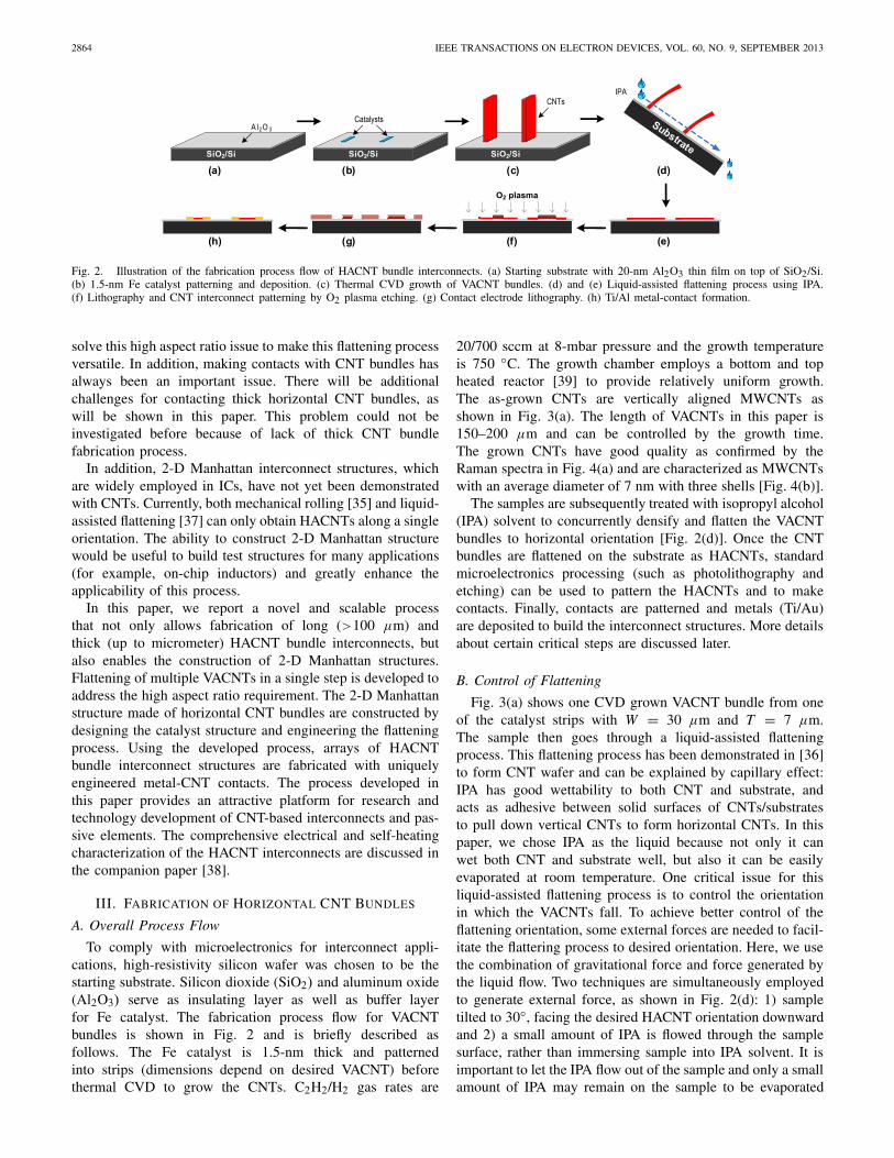
Fig. 2. Illustration of the fabrication process flow of HACNT bundle interconnects. (a) Starting substrate with 20-nm Al2O3 thin film on top of SiO2/Si.(b) 1.5-nm Fe catalyst patterning and deposition. (c) Thermal CVD growth of VACNT bundles. (d) and (e) Liquid-assisted flattening process using IPA.(f) Lithography and CNT interconnect patterning by O2 plasma etching. (g) Contact electrode lithography. (h) Ti/Al metal-contact formation.
solve this high aspect ratio issue to make this flattening processversatile. In addition, making contacts with CNT bundles hasalways been an important issue. There will be additionalchallenges for contacting thick horizontal CNT bundles, aswill be shown in this paper. This problem could not beinvestigated before because of lack of thick CNT bundlefabrication process.
In addition, 2-D Manhattan interconnect structures, whichare widely employed in ICs, have not yet been demonstratedwith CNTs. Currently, both mechanical rolling [35] and liquid-assisted flattening [37] can only obtain HACNTs along a singleorientation. The ability to construct 2-D Manhattan structurewould be useful to build test structures for many applications(for example, on-chip inductors) and greatly enhance theapplicability of this process.
In this paper, we report a novel and scalable processthat not only allows fabrication of long (>100 μm) andthick (up to micrometer) HACNT bundle interconnects, butalso enables the construction of 2-D Manhattan structures.Flattening of multiple VACNTs in a single step is developed toaddress the high aspect ratio requirement. The 2-D Manhattanstructure made of horizontal CNT bundles are constructed bydesigning the catalyst structure and engineering the flatteningprocess. Using the developed process, arrays of HACNTbundle interconnect structures are fabricated with uniquelyengineered metal-CNT contacts. The process developed inthis paper provides an attractive platform for research andtechnology development of CNT-based interconnects and pas-sive elements. The comprehensive electrical and self-heatingcharacterization of the HACNT interconnects are discussed inthe companion paper [38].
III. FABRICATION OF HORIZONTAL CNT BUNDLES
A. Overall Process Flow
To comply with microelectronics for interconnect appli-cations, high-resistivity silicon wafer was chosen to be thestarting substrate. Silicon dioxide (SiO2) and aluminum oxide(Al2O3) serve as insulating layer as well as buffer layerfor Fe catalyst. The fabrication process flow for VACNTbundles is shown in Fig. 2 and is briefly described asfollows. The Fe catalyst is 1.5-nm thick and patternedinto strips (dimensions depend on desired VACNT) beforethermal CVD to grow the CNTs. C2H2/H2 gas rates are
20/700 sccm at 8-mbar pressure and the growth temperatureis 750 ◦C. The growth chamber employs a bottom and topheated reactor [39] to provide relatively uniform growth.The as-grown CNTs are vertically aligned MWCNTs asshown in Fig. 3(a). The length of VACNTs in this paper is150–200 μm and can be controlled by the growth time.The grown CNTs have good quality as confirmed by theRaman spectra in Fig. 4(a) and are characterized as MWCNTswith an average diameter of 7 nm with three shells [Fig. 4(b)].
The samples are subsequently treated with isopropyl alcohol(IPA) solvent to concurrently densify and flatten the VACNTbundles to horizontal orientation [Fig. 2(d)]. Once the CNTbundles are flattened on the substrate as HACNTs, standardmicroelectronics processing (such as photolithography andetching) can be used to pattern the HACNTs and to makecontacts. Finally, contacts are patterned and metals (Ti/Au)are deposited to build the interconnect structures. More detailsabout certain critical steps are discussed later.
B. Control of Flattening
Fig. 3(a) shows one CVD grown VACNT bundle from oneof the catalyst strips with W = 30 μm and T = 7 μm.The sample then goes through a liquid-assisted flatteningprocess. This flattening process has been demonstrated in [36]to form CNT wafer and can be explained by capillary effect:IPA has good wettability to both CNT and substrate, andacts as adhesive between solid surfaces of CNTs/substratesto pull down vertical CNTs to form horizontal CNTs. In thispaper, we chose IPA as the liquid because not only it canwet both CNT and substrate well, but also it can be easilyevaporated at room temperature. One critical issue for thisliquid-assisted flattening process is to control the orientationin which the VACNTs fall. To achieve better control of theflattening orientation, some external forces are needed to facil-itate the flattering process to desired orientation. Here, we usethe combination of gravitational force and force generated bythe liquid flow. Two techniques are simultaneously employedto generate external force, as shown in Fig. 2(d): 1) sampletilted to 30◦, facing the desired HACNT orientation downwardand 2) a small amount of IPA is flowed through the samplesurface, rather than immersing sample into IPA solvent. It isimportant to let the IPA flow out of the sample and only a smallamount of IPA may remain on the sample to be evaporated

LI et al.: LOW-RESISTIVITY LONG-LENGTH HORIZONTAL CNT BUNDLES 2865
Fig. 3. (a) As-grown VACNT bundle from catalyst dimension W = 30 μmand T = 7 μm. (b) HACNT bundle obtained after flattening process.(c) HACNT bundle array showing good control of flattening orientation.(d) Zoom-in image of one of the HACNT bundles in (c).
Fig. 4. (a) Raman spectra of as-grown CNTs, indicating MWCNT (no radialbreathing mode observed) and good quality (high G/D ratio). (b) TEM imageof an as-grown CNT, showing 6–8-nm diameter and three shells.
out. Both tilted sample and the IPA surface flow help todirect the orientation of the flattening process by contributingadditional forces to the desired orientation. After flatteningprocess, HACNT bundle arrays are formed on the substratewith good alignment as shown in Fig. 3(c). Note that thisliquid-assisted process also densifies the CNT bundle, as hasbeen reported in [40]. In this paper, the density of CNTs afterIPA treatment was enhanced by ∼45 times (densification ratioDR = 45) as evidenced from atomic force microscope (AFM)measurement shown in Fig. 5. The width of HACNTs afterflattening almost remained the same as the W of the VACNTs.
It should be noted that to make sure that CNT bundles areflattened in a particular orientation, it is also important to havecatalyst strip with high aspect ratio (W/T ), as described inSection II. Larger W implies larger surface, which introduceslarger surface tension on W side than that on T side, soVACNT is more likely to flatten perpendicular to the Wside. If W and T are similar, then surface tensions on bothsides are similar, and there is no preference on the flatteningorientation. From our experiments, with reasonable W/T ratio(>3), vertical CNT bundles were found to be flattened in theorientation perpendicular to W , which is desired.
C. Obtaining Thick HACNTs
Because of the requirement of relatively large W/T ratioand shrinking in thickness after flattening, it is difficultto obtain CNT bundles with large thickness (of the orderof micrometer). To overcome this limitation, we introduce
Fig. 5. (a) 3-D profile, measured by AFM, of one HACNT after flattening.(b) Thickness measured by AFM [along the red line in the SEM image shownin the inset figure in (b)]. The measured HACNT bundle was obtained afterflattening a VACNT bundle with W = 30 μm and T = 10 μm. The width ofHACNT remained approximately the same as that of the VACNT. The averagethickness of the HACNT is measured to be ∼220 nm, which indicates adensification of 45X.
Fig. 6. (a) and (b) Three and four VACNTs grown next to each other for thepurpose of obtaining thick HACNTs. (c) and (d) Thick HACNTs obtainedafter single flattening process from (a) and (b), respectively. Each VACNTshown in (a) and (b) has a width W = 30 μm and thickness T = 7 μm.
multiple VACNT flattening in a single step to obtain largethickness HACNTs. Instead of using one VACNT to form oneHACNT, multiple VACNTs are designed to be flattened ontop of each other to form one thick HACNT as shown inFig. 6. Each as-grown VACNT still has large W/T ratio toensure the flattening orientation. The overlapping regions ofthe HACNTs have greater thickness depending on the numberof VACNTs. The root and tip of CNT bundles are clearlyobservable and the number of VACNTs can be identified in thefigure. Using this multiple VACNT flattening process, the totalW/T ratio is no longer needed to be large. We successfullyfabricated W = 30 μm with total T = 40 μm (4 × 10 μm inparallel), which yielded a thickness of ∼1 μm after flatteningand densification. Note that the concept of using multipleVACNTs in parallel should also work for the mechanicalrolling-based flattening approach.
Although we are able to fabricate thick HACNTs by catalystpatterning and process engineering, our current process mayencounter scalability issue as it would be quite challenging toflatten lines with small widths (<1 μm) while maintainingreasonable thickness. With some postprocessing, there arepathways to address this issue. For instance, one can first

2866 IEEE TRANSACTIONS ON ELECTRON DEVICES, VOL. 60, NO. 9, SEPTEMBER 2013
Fig. 7. (a) Placement of VACNTs for constructing Manhattan structures with liquid flow along the directions indicated by the solid yellow arrow. Brokenyellow arrows indicate the orientation of flattening. (b) 2-D Manhattan structure1 obtained after flattening of the four VACNTs in (a). (c) Spiral inductorformed with metal contacts based on a Manhattan structure.
fabricate large width HACNTs with desired thickness andthen pattern them to achieve the desired smaller widths. Manyfuture engineering and development research can be carriedout along this direction.
D. Constructing 2-D Manhattan Structures
The 2-D Manhattan structures involve perpendicularlyaligned interconnect structures and are commonly used incurrent back-end layout designs to achieve the shortest-pathcommunication between logic gates [41]. The most commonway to achieve this is to orient adjacent interconnect layers inperpendicular directions by connecting through vertical vias.
For CNT interconnects, fabricating single orientationinterconnect is challenging enough, let alone making 2-DManhattan structures. In this paper, we demonstrate howto overcome this challenge and build Manhattan structuresfor the first time. Based on the understanding of the liquid-assisted flattening process, we further develop a process thatcould successfully construct 2-D Manhattan structures in asingle step by suitably engineering the catalyst design andflattening process. Fig. 7(a) shows the placement of as-grownVACNTs, and Fig. 7(b) shows the obtained Manhattanstructure. The liquid flows from the top as shown in Fig. 7(a),which provides forces to flatten two VACNTs in perpendiculardirections. Once the Manhattan structure is obtained, standardlithography can be used to pattern and build useful structures.Fig. 7(c) shows an example of using a Manhattan structure tobuild a planar spiral inductor that can be useful for designingvarious on-chip CNT-bundle-based inductors.
IV. OBTAINING GOOD CONTACTS TO
THICK CNT BUNDLES
Making good contact to CNTs is always a challeng-ing issue for both CNT-based transistors and interconnects.From process point of view, making good contacts to large-thickness horizontal CNT bundles has some additional issuesthat may not be encountered in the case of transistors or
1This is also the first demonstration of a Kanji character (meaning “father”)using any form of carbon nanostructures.
Fig. 8. (a) Ideal metal-HACNT contact with metal physically connectingthe ends of each CNT within the HACNT bundle. (b) Partial metal-HACNTcontact with voids between metal and CNTs. (c) Thick HACNT would likelyhave PR residue at the bottom of CNT bundle as CNTs are good lightabsorbers. (d) Nonideal vertical HACNT edge profile after etching couldintroduce voids between metal and HACNTs.
vertical vias. As shown in Fig. 8(a), an ideal contact shouldhave metal physically contacting both sides as well as theends of each CNT in the bundle. Because of the fact thatCNTs are not completely transparent, thick CNT bundleswill, however, block the laser from penetrating to the bottomof the bundle during photolithography. Therefore, after theexposure and develop step, there is considerable photoresist(PR) residue remaining near the bottom edge of the CNTbundles [Fig. 8(c)]. These PR residues prevent from makinggood contacts to the CNT bundles during the subsequentmetal deposition. In fact, even if there is no PR residue, thethick CNT bundles themselves would also prevent metal fromreaching the bottom part of the bundles during the metaldeposition (mostly perpendicular deposition, such as usinge-beam evaporator), as shown in Fig. 8(b) where only theupper part of HACNT bundle is covered by metal. Thisissue does not exist for CNT array transistors because theyemploy monolayer CNTs. It is significant when the bun-dle is reasonably thick (>100 nm). In addition, during theCNT patterning process, CNT bundles may not be etchedabsolutely vertically with respect to the substrate [Fig. 8(d)].

LI et al.: LOW-RESISTIVITY LONG-LENGTH HORIZONTAL CNT BUNDLES 2867
Fig. 9. (a) Using a two-layer PR process with standard PR (second PR) ontop of PMGI, which can only be exposed under DUV. The top layer is usedto define the electrode pads and also serves as a mask for exposing PMGIunder DUV. PMGI can be exposed and developed for multiple times untilno PR residue is left. After multiple exposures, a PR undercut profile is alsoformed, which facilitates the lift-off process in the next step. (b) Sample istilted and rotated simultaneously during metal deposition to make good fullmetal-CNT contact at both ends of the HACNT bundle.
1mm
Fig. 10. Test structure array with total of 54 devices with different widths,lengths, and thickness of CNT bundle interconnects. All of the HACNTinterconnects in the test structure array show good horizontal alignment.
Therefore, any undercut or imperfect edge will inducevoid between metal and CNTs, leading to partial contacts[Fig. 8(b)]. This issue does not exist for either CNT arraytransistors (thin CNTs) or vertical CNT vias, where chemicalmechanical polishing process is used to open up all the shellsin each CNT to form good metal contacts.
To make good full contact between CNT bundle and metal,we first employed a two layer PR process to overcome thePR residue issue [Fig. 9(a)]. The bottom (first) PR layerin contact with the CNTs is polymethylglutarimide (PMGI),which can only be exposed by deep ultraviolet (DUV) andthe top (second) PR layer can be any standard PR (AZ4110in this work). After first exposure and develop of AZ4110,the unexposed top PR layer serves as a mask for subsequentexposure of bottom PMGI layer under DUV. Because thecontact region is defined by first layer, we can expose anddevelop PMGI multiple times until there is no notable PRresidue at the bottom of HACNT bundles. Note that increasingexposure and develop time for PMGI layer only increases theundercut of bottom PR layer and not the contact window. Thistwo layer PR process not only solves the PR residue issue, butalso provides an undercut PR profile, which also facilitates thesubsequent lift-off step after contact metal deposition. Havingundercut profile also allows the samples to be tilted duringmetal deposition [Fig. 9(b)].
This tilted configuration exposes the lower most part of theHACNT bundle to metal beams during metal deposition, evenif the HACNT edge is not perfectly vertical, thereby preventing
Fig. 11. Set of measurements of resistance from CNT interconnect TLMstructure with same width but four different thicknesses. W30-T7 indicatesthat the VACNT before flattening had W = 30 μm, T = 7 μm. The numbersafter T7× indicate the number of VACNTs before being flattened to form oneHACNT.
possible voids between CNT and metal. In addition, the samplestage is rotated during metal deposition so that both ends ofHACNT are exposed to the metal beam. Through combiningtwo layer PR process as well as tilting and rotating the stageduring metal deposition, all CNTs in the thick HACNT bundleget in full contact with metal thereby forming good contactconfiguration. In this paper, 500/1000-nm thick Ti/Au stack isdeposited as contact electrode without any lift-off problem.
V. FABRICATION OF HACNT INTERCONNECT ARRAY
Using this process, test structures were fabricated withvarious CNT interconnect length, width, and thickness. Fig. 10shows an array of 54 devices (six rows and nine columns),where all HACNT bundles are flattened in the same ori-entation. It should be noted that this process also allowscofabrication of CNT bundle with different thickness, whichcan be beneficial for designing both interconnects and passiveson the same layer. For the same width and thickness, the lengthof CNT interconnects were varied from 10 to 130 μm. UsingTLM-like technique [42], the resistance of CNT interconnectswith different lengths was measured, and the resistance perunit length (Rp.u.l) and contact resistance (Rcont) of CNTinterconnect for a given width and thickness were extractedusing the equation as follows:
Rmeas = Rp.u.l × L + 2Rcont (1)
where Rmeas is the measured resistance for a given lengthL of CNT interconnect. Fig. 11 shows an example of themeasurement data for four different CNT interconnect thick-ness with fixed line width W = 30 μm. Similar to the CNTbundles shown in Fig. 6, the CNT interconnects measured inFig. 11 were flattened from one to four VACNT bundles (eachVACNT bundle has W = 30 μm, T = 7 μm). Each datapoint in Fig. 11 is the average measured value from threeto six devices (deviations of data points are mostly <10%).Even though all the CNT interconnects are individual devices,the data points display clear linear relationship, which indi-cates that the HACNTs have reasonably uniform spatial den-sity, which in turn implies success of our TLM-like teststructure fabrication and measurements.

2868 IEEE TRANSACTIONS ON ELECTRON DEVICES, VOL. 60, NO. 9, SEPTEMBER 2013
TABLE I
EXTRACTED RESISTANCE AND CONTACT RESISTANCE OF FABRICATED HACNT ARRAYS
CNT Interconnects W30-T7 W30-T7x2 W30-T7x3 W30-T7x4 W40-T10 W40-T10x2 W40-T10x3 W40-T10x4
Resistance p.u.l. (Ω/μm) 8.036 3.555 2.488 1.957 2.616 1.306 0.871 0.681Contact Resistance (Ω) 52.9785 16.05 13.9865 11.6485 38.0415 21.022 15.5555 13.4895Unit Area Contact Resistance (Ω-m2) * 2.47E-10 1.5E-10 1.96E-10 2.17E-10 3.38E-10 3.74E-10 4.15E-10 4.8E-10
* Calculation is based on the assumption that the densification ratio is 45, as indicated in Fig. 5.
The extracted resistance per unit length and contact resis-tance are shown in Table I. It can be observed from theextracted resistances that the overall resistance per unit lengthand the contact resistance, in general, scale with the crosssection of the HACNTs. The resistance per unit length is moreor less inversely proportional to the thickness as expected,indicating the feasibility and success of the process of makingfull metal-CNT-bundle contact discussed in Section IV. Theunit area contact resistance is calculated to be on the order of1 E–10 �-m2. Table I also shows the results for catalyst stripwith W = 40 μm and T = 10 μm. For this configuration,the thickness of CNT bundle can reach up to micrometerthickness when there are three or four catalyst strips. Becauseof larger thickness and width, both per unit length and contactresistances are generally smaller than those HACNTs withW = 30 μm and T = 7 μm. In part II, we provide morediscussions on the electrical data and show that the resistivityof our CNTs is between 1.7 and 4.1 m�-cm [38].
VI. CONCLUSION
To summarize, in this paper, thick (∼1 μm) HACNTinterconnects with lengths (>100 μm) have been demon-strated by designing novel catalyst structures and using aliquid-assisted flattening process. The developed process alsoenables construction of 2-D Manhattan structures in a singlestep, thereby opening up endless possibilities of realizingCNT-based on-chip passive elements such as angled inter-connects, inductors, and antennas in next-generation inte-grated circuits and systems. Special process has also beendeveloped to make full metal contact with thick horizontalCNT bundles. Through fabricated test structures, the per unitlength resistance and contact resistance of CNT intercon-nects were extracted using TLM-like measurements, indicatingthe success of the process. The ability to fabricate longand thick horizontal CNT interconnects not only fills thegap between CNT interconnect modeling and experimentalefforts, but also provides an important vehicle to study cer-tain fundamental properties of CNT bundles, such as theirunique high-frequency properties (i.e., reduced skin effect), aswell as extraction of relevant parameters. This experimentaldemonstration also opens up pathways for exploring manyother process options (such as metal-filled CNT bundles) andapplications (such as chip-to-chip interconnections, off-chipthermal bumps/links for efficient packaging, and heat sinking),as well as embedded energy-storage devices in emerging 3-Dintegrated circuits.
ACKNOWLEDGMENT
All process steps for device fabrication were carried outusing the Nanostructure Cleanroom Facility at the California
NanoSystems Institute and the Nanofabrication Facilities atUCSB - part of the National Nanotechnology InfrastructureNetwork. K.B. thanks the Alexander von Humboldt Founda-tion in Germany for the F.W. Bessel Research Award thatgreatly facilitated many stimulating discussions with F.K. inMünchen.
REFERENCES
[1] K. Banerjee, “Global (interconnect) warming,” IEEE Circuits DevicesMag., vol. 17, no. 5, pp. 16–32, Sep. 2001.
[2] N. Srivastava and K. Banerjee, “Interconnect challenges for nanoscaleelectronic circuits,” JOM, vol. 56, pp. 30–31, Oct. 2004.
[3] J. Hone, M. Whitney, C. Piskoti, and A. Zettl, “Thermal conduc-tivity of single-walled carbon nanotubes,” Phys. Rev. B, vol. 59,pp. R2514–R2516, Jan. 1999.
[4] B. Q. Wei, R. Vajtai, and P. M. Ajayan, “Reliability and currentcarrying capacity of carbon nanotubes,” Appl. Phys. Lett., vol. 79, no. 8,pp. 1172–1174, Aug. 2001.
[5] F. Li, H. M. Cheng, S. Bai, G. Su, and M. S. Dresselhaus, “Tensilestrength of single-walled carbon nanotubes directly measured from theirmacroscopic ropes,” Appl. Phys. Lett., vol. 77, no. 20, pp. 3161–3163,2000.
[6] N. Srivastava, H. Li, F. Kreupl, and K. Banerjee, “On the applicabilityof single-walled carbon nanotubes as VLSI interconnects,” IEEE Trans.Nanotechnol., vol. 8, no. 4, pp. 542–559, Jul. 2009.
[7] H. Li, C. Xu, and K. Banerjee, “Carbon nanomaterials: The idealinterconnect technology for next-generation ICs,” IEEE Design TestComput., vol. 27, no. 4, pp. 20–31, Jul./Aug. 2010.
[8] H. Li, N. Srivastava, J.-F. Mao, W.-Y. Yin, and K. Banerjee, “Carbonnanotube vias: Does ballistic electron and phonon transport implyimproved performance and reliability?” IEEE Trans. Electron Devices,vol. 58, no. 4, pp. 2689–2701, Jul./Aug. 2011.
[9] F. Kreupl, A. P. Graham, G. S. Duesberg, W. Steinhogl, M. Liebau,E. Unger, and W. Honlein, “Carbon nanotubes in interconnect applica-tions,” Microelectron. Eng., vol. 64, pp. 399–408, Oct. 2002.
[10] J. Li, Q. Ye, A. Cassell, H. T. Ng, R. Stevens, J. Han, and M. Meyyappan,“Bottom-up approach for carbon nanotube interconnects,” Appl. Phys.Lett., vol. 82, pp. 2491–2493, Apr. 2003.
[11] M. Nihei, D. Kondo, A. Kawabata, S. Sato, H. Shioya, M. Sakaue,T. Iwai, M. Ohfuti, and Y. Awano, “Low-resistance multi-walled car-bon nanotube vias with parallel channel conduction of inner shells[IC interconnect applications],” in Proc. IEEE IITC, Jun. 2005,pp. 234–236.
[12] H. Li, C. Xu, N. Srivastava, and K. Banerjee, “Carbon nanomaterialsfor next-generation interconnects and passives: Physics, status, andprospects,” IEEE Trans. Electron Devices, vol. 56, no. 9, pp. 1799–1821,Sep. 2009.
[13] A. Naeemi and J. D. Meindl, “Design and performance modelingfor single-walled carbon nanotubes as local, semiglobal, and globalinterconnects in gigascale integrated systems,” IEEE Trans. ElectronDevices, vol. 54, no. 1, pp. 26–37, Jan. 2007.
[14] H. Li, W. Y. Yin, K. Banerjee, and J. F. Mao, “Circuit modeling andperformance analysis of multi-walled carbon nanotube interconnects,”IEEE Trans. Electron Devices, vol. 55, no. 6, pp. 1328–1337, Jun. 2008.
[15] C. Xu, H. Li, R. Suaya, and K. Banerjee, “Compact AC modeling andperformance analysis of through-silicon vias (TSVs) in 3-D ICs,” IEEETrans. Electron Devices, vol. 57, no. 12, pp. 3405–3417, Dec. 2010.
[16] H. Li and K. Banerjee, “High-frequency analysis of carbon nanotubeinterconnects and implications for on-chip inductor design,” IEEE Trans.Electron Devices, vol. 56, no. 10, pp. 2202–2214, Oct. 2009.

LI et al.: LOW-RESISTIVITY LONG-LENGTH HORIZONTAL CNT BUNDLES 2869
[17] M. Nihei, T. Hyakushima, S. Sato, T. Nozue, M. Norimatsu,M. Mishima, T. Murakami, D. Kondo, A. Kawabata, M. Ohfuti, andY. Awano, “Electrical properties of carbon nanotube via interconnectsfabricated by novel damascene process,” in Proc. IEEE InterconnectTechnol. Conf., Jun. 2007, pp. 204–206.
[18] J. Dijon, H. Okuno, M. Fayolle, T. Vo, J. Pontcharra, D. Acquaviva,D. Bouvet, A. M. Ionescu, C. S. Esconjauregui, B. Capraro, E. Quesnel,and J. Robertson, “Ultra-high density carbon nanotubes on Al-Cu foradvanced vias,” in Proc. IEDM, Dec. 2010, pp. 33.4.1–33.4.4.
[19] A. Kawabata, S. Sato, T. Nozue, T. Hyakushima, M. Norimatsu,M. Mishima, T. Murakami, D. Kondo, K. Asano, M. Ohfuti,H. Kawarada, T. Sakai, M. Nihei, and Y. Awano, “Robustness of CNTvia interconnect fabricated by low temperature process over a high-density current,” in Proc. IEEE IITC, Jun. 2008, pp. 237–239.
[20] K. Banerjee and A. Mehrotra, “A power-optimal repeater insertionmethodology for global interconnects in nanometer designs,” IEEETrans. Electron Devices, vol. 49, no. 11, pp. 2001–2007, Nov. 2002.
[21] (2010). International Technology Roadmap for Semiconductors (ITRS)[Online]. Available: http://public.itrs.net/
[22] B. Q. Wei, R. Vajtai, Y. Jung, J. Ward, R. Zhang, G. Ramanath, andP. M. Ajayan, “Organized assembly of carbon nanotubes—Cunningrefinements help to customize the architecture of nanotube structures,”Nature, vol. 416, pp. 495–496, Apr. 2002.
[23] C. Zhang, D. Cott, N. Chiodarelli, P. Vereecken, J. Robertson, andC. M. Whelan, “Growth of carbon nanotubes as horizontal intercon-nects,” Solid State Phys., vol. 245, pp. 2308–2310, Oct. 2008.
[24] F. Yan, C. Zhang, D. Cott, G. Zhong, and J. Robertson, “High-densitygrowth of horizontally aligned carbon nanotubes for interconnects,”Solid State Phys., vol. 247, pp. 2669–2672, Dec. 2010.
[25] J. Y. Lu, J. M. Miao, T. Xu, B. Yan, T. Yu, and Z. X. Shen, “Growthof horizontally aligned dense carbon nanotubes from trench sidewalls,”Nanotechnology, vol. 22, no. 26, p. 265614, Nov. 2011.
[26] Y. G. Zhang, A. L. Chang, J. Cao, Q. Wang, W. Kim, Y. M. Li,N. Morris, E. Yenilmez, J. Kong, and H. J. Dai, “Electric-field-directedgrowth of aligned single-walled carbon nanotubes,” Appl. Phys. Lett.,vol. 79, pp. 3155–3157, Nov. 2001.
[27] J. B. K. Law, C. K. Koo, and J. T. L. Thong, “Horizontally directedgrowth of carbon nanotubes utilizing self-generated electric field fromplasma induced surface charging,” Appl. Phys. Lett., vol. 91, no. 24,pp. 243108-1–243108-3, Dec. 2007.
[28] Y. Chai, Z. Y. Xiao, and P. C. H. Chan, “Electron-shading effect onthe horizontal aligned growth of carbon nanotubes,” Appl. Phys. Lett.,vol. 94, no. 4, pp. 043116-1–043116-3, Jan. 2009.
[29] Z. Jin, H. B. Chu, J. Y. Wang, J. X. Hong, W. C. Tan, and Y. Li,“Ultralow feeding gas flow guiding growth of large-scale horizontallyaligned single-walled carbon nanotube arrays,” Nano Lett., vol. 7,pp. 2073–2079, Jul. 2007.
[30] S. M. Huang, X. Y. Cai, and J. Liu, “Growth of millimeter-long andhorizontally aligned single-walled carbon nanotubes on flat substrates,”J. Amer. Chem. Soc., vol. 125, pp. 5636–5637, May 2003.
[31] G. F. Close, S. Yasuda, B. Paul, S. Fujita, and H. S. P. Wong,“A 1 GHz integrated circuit with carbon nanotube interconnects andsilicon transistors,” Nano Lett., vol. 8, pp. 706–709, Feb. 2008.
[32] A. Tselev, M. Woodson, C. Qian, and J. Liu, “Microwave impedancespectroscopy of dense carbon nanotube bundles,” Nano Lett., vol. 8,pp. 152–156, Jan. 2008.
[33] S. J. Kang, C. Kocabas, T. Ozel, M. Shim, N. Pimparkar, M. A. Alam,S. V. Rotkin, and J. A. Rogers, “High-performance electronics usingdense, perfectly aligned arrays of single-walled carbon nanotubes,”Nature Nanotechnol., vol. 2, pp. 230–236, Apr. 2007.
[34] W. W. Zhou, L. Ding, S. W. Yang, and J. Liu, “Orthogonal orientationcontrol of carbon nanotube growth,” J. Amer. Chem. Soc., vol. 132,pp. 336–341, Jan. 2010.
[35] S. Tawfick, K. O’Brien, and A. J. Hart, “Flexible high-conductivitycarbon-nanotube interconnects made by rolling and printing,” Small,vol. 5, pp. 2467–2473, Nov. 2009.
[36] Y. Hayamizu, T. Yamada, K. Mizuno, R. C. Davis, D. N. Futaba,M. Yumura, and K. Hata, “Integrated three-dimensional microelectro-mechanical devices from processable carbon nanotube wafers,” NatureNanotechnol., vol. 3, pp. 289–294, May 2008.
[37] M. H. Sun, Z. Y. Xiao, Y. Chai, Y. A. Li, and P. C. H. Chan, “Inductanceproperties of in situ-grown horizontally aligned carbon nanotubes,” IEEETrans. Electron Devices, vol. 58, no. 1, pp. 229–235, Jan. 2011.
[38] H. Li, W. Liu, A. M. Cassell, F. Kreupl, and K. Banerjee, “Low-resistivity long-length horizontal carbon nanotube bundles for inter-connect applications—Part II: Characterization,” IEEE Trans. ElectronDevices, vol. 60, no. 9, pp. 2870–2876, Sep. 2013.
[39] W. Liu, H. Li, C. Xu, Y. Khatami, and K. Banerjee, “Synthesis of high-quality monolayer and bilayer graphene on copper using chemical vapordeposition,” Carbon, vol. 49, no. 13, pp. 4122–4030, 2011.
[40] D. N. Futaba, K. Hata, T. Yamada, T. Hiraoka, Y. Hayamizu, Y. Kaku-date, O. Tanaike, H. Hatori, M. Yumura, and S. Iijima, “Shape-engineerable and highly densely packed single-walled carbon nanotubesand their application as super-capacitor electrodes,” Nature Mater.,vol. 5, pp. 987–994, Dec. 2006.
[41] J. Cong, “An interconnect-centric design flow for nanometer technolo-gies,” Proc. IEEE, vol. 89, no. 4, pp. 505–528, Apr. 2001.
[42] D. K. Schroder, Semiconductor Material And Device Characterization,3rd ed. New York, NY, USA: Wiley, 2006.
Hong Li (S’07–M’12) received the Ph.D. degreein electrical and computer engineering from theUniversity of California, Santa Barbara, CA, USA,in 2012.
He is currently an Emerging Memory Engineerwith Micron Technology, Inc., Boise, ID, USA.
Wei Liu (M’10) received the Ph.D. degree inchemistry from the Institute of Chemistry, ChineseAcademy of Sciences, Beijing, China, in 2008.
He is currently a Post-Doctoral Research Scholarwith the University of California, Santa Barbara,CA, USA.
Alan M. Cassell received the Ph.D. degree inmaterials chemistry from the University of SouthCarolina, Columbia, SC, USA, in 1998.
He is currently an Aerospace Engineer at EntrySystems and Vehicle Development Branch, NASAAmes Research Center, Mountain View, CA, USA.
Franz Kreupl (M’04) is a Professor of elec-trical engineering with Technische UniversitaetMuenchen, Muenchen, Germany.
Kaustav Banerjee (S’92–M’99–SM’03–F’12) is aProfessor of electrical and computer engineeringwith the University of California, Santa Barbara,CA, USA.