Chapter #2: Two-Level Combinational Logic Section 2.1, 2.2 -- Logic Functions and Gates
Upload
joan-woodsCategory
view
224download
4
Logic Gates Logic gates are electronic digital circuit
perform logic functions. Commonly expected logic functions are already having the corresponding logic circuits in Integrated Circuit (I.C.) form.
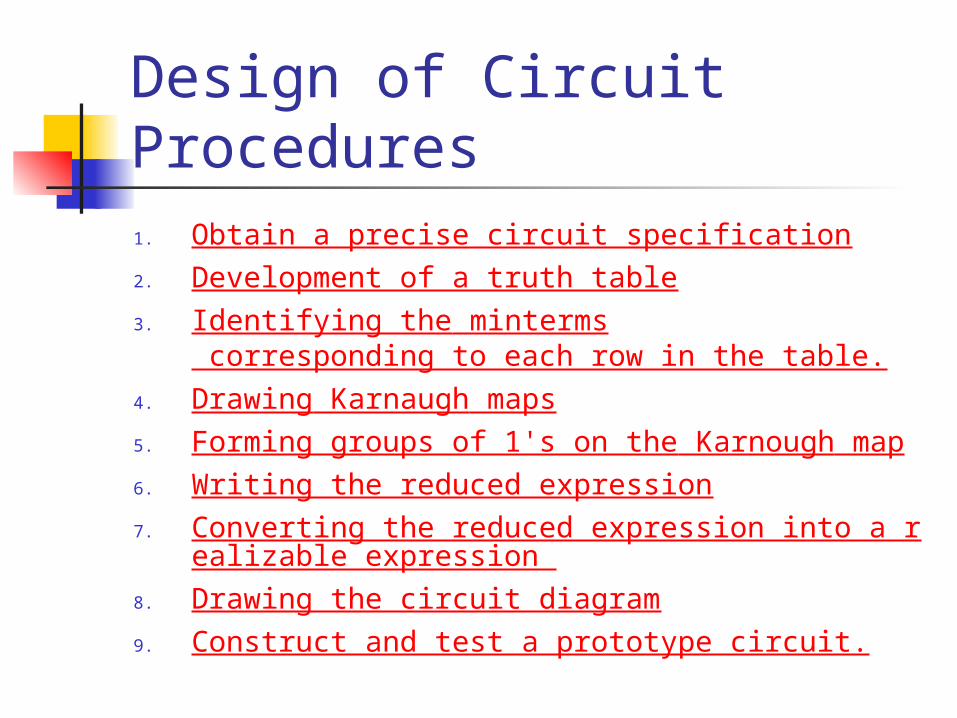
Design of Circuit Procedures1. Obtain a precise circuit specification 2. Development of a truth table 3. Identifying the minterms
corresponding to each row in the table. 4. Drawing Karnaugh maps 5. Forming groups of 1's on the Karnough map 6. Writing the reduced expression 7. Converting the reduced expression into a rea
lizable expression 8. Drawing the circuit diagram 9. Construct and test a prototype circuit.
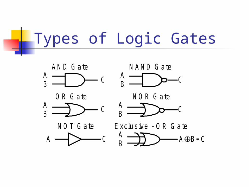
Types of Logic Gates
AN D G ate
O R G ate
N O T G ate
AB C
AB C
A C
N AN D G ateAB C
N O R G ateAB C
Exclusive - O R G ateAB A B=C
Basic Gates
AND , OR , NOT
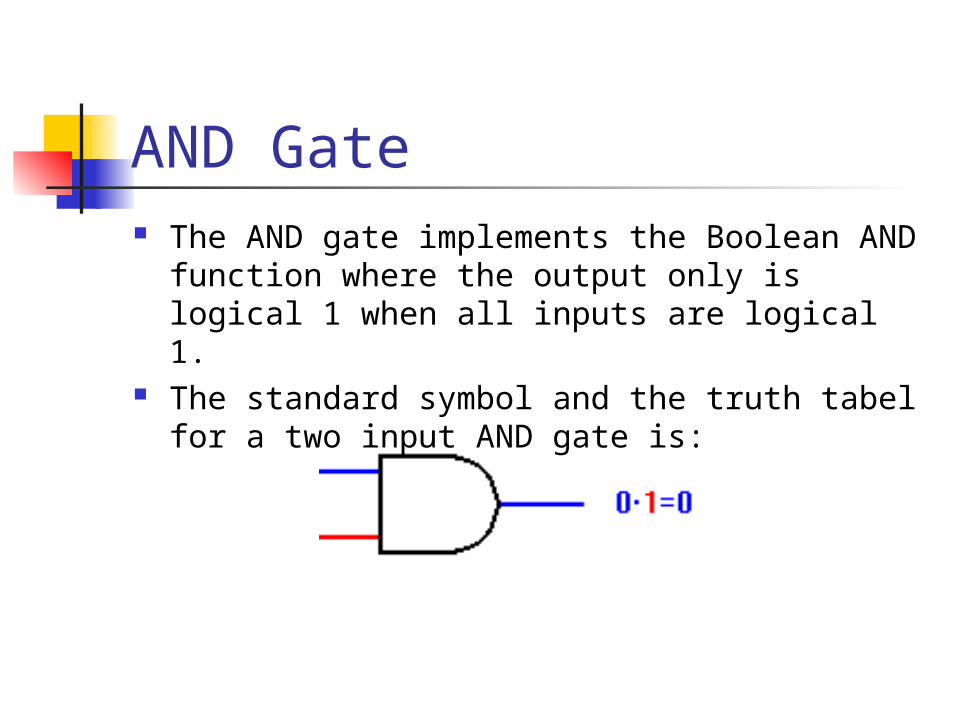
AND Gate The AND gate implements the Boolean AND
function where the output only is logical 1 when all inputs are logical 1.
The standard symbol and the truth tabel for a two input AND gate is:
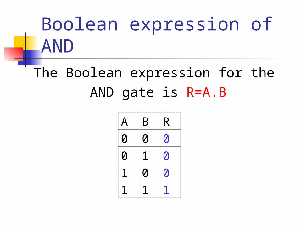
Boolean expression of AND
The Boolean expression for the AND gate is R=A.B
A B R
0 0 0
0 1 0
1 0 0
1 1 1

OR Gate The OR gate implements the Boolean
OR function where the output is logical 1 when just input is logical 1.
The standard symbol and the truth table for a two input OR gate is:

Boolean Expression of OR
A B R
0 0 0
0 1 1
1 0 1
1 1 1
The Boolean expression for the OR gate is: R=A+B
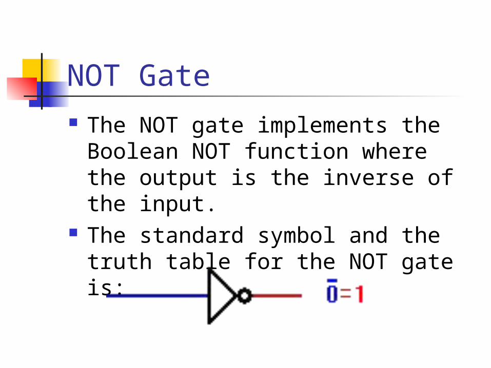
NOT Gate The NOT gate implements the
Boolean NOT function where the output is the inverse of the input.
The standard symbol and the truth table for the NOT gate is:

Boolean Expression of NOT The Boolean expression for the
NOT gate is: R=-A
A R
0 1
0 0

Derived Gates
NAND , NOR , XOR

NAND Gate The NAND gate is an AND gate followed by a
NOT gate. The output is logical 1 when one of the inputs are logical 0
The standard symbol and the truth table for the NAND gate is:

Boolean expression of NAND
A B R
0 0 1
0 1 1
1 0 1
1 1 0
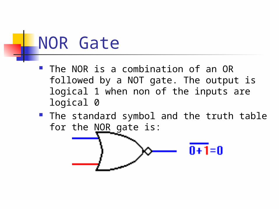
NOR Gate The NOR is a combination of an OR followed by
a NOT gate. The output is logical 1 when non of the inputs are logical 0
The standard symbol and the truth table for the NOR gate is:

Boolean Expression of NOR
A B R
0 0 1
0 1 0
1 0 0
1 1 0
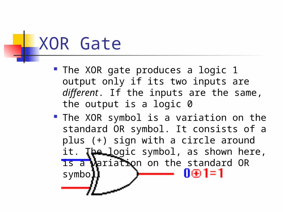
XOR Gate The XOR gate produces a logic 1 output only
if its two inputs are different. If the inputs are the same, the output is a logic 0
The XOR symbol is a variation on the standard OR symbol. It consists of a plus (+) sign with a circle around it. The logic symbol, as shown here, is a variation on the standard OR symbol.

Exercise 1
http://kom.auc.dk/logic/
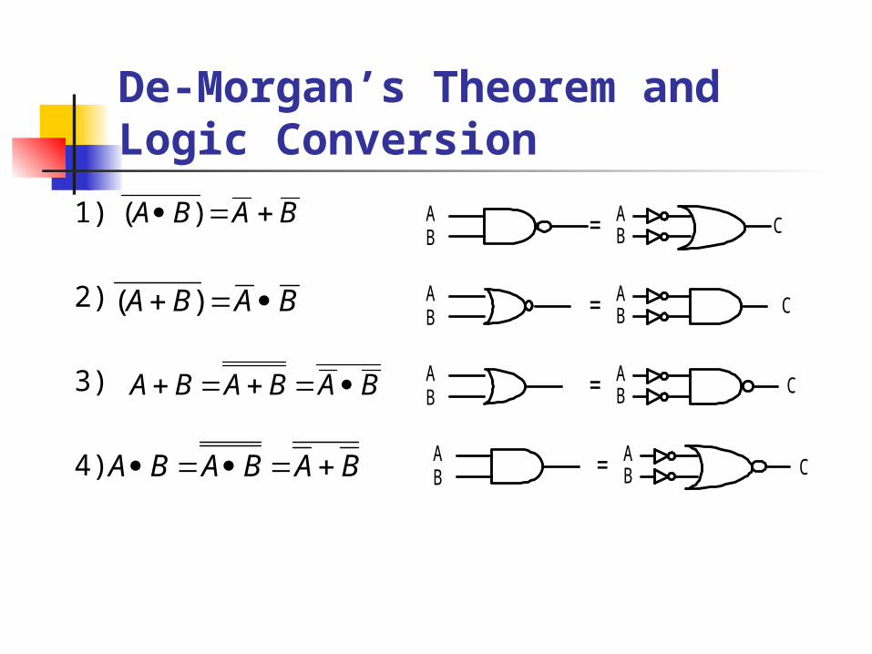
De-Morgan’s Theorem and Logic Conversion
1)
2)
3)
4)
BABA )( AB
AB C=
BABA )( AB
AB C=
BABABA
BABABA
AB
AB C=
AB
AB C=

Implement the logic expression using NAND gates only
ZYX
ZYX
ZYX
Z1)
ZYZXXY
ZYZXXY
ZYZXXY
Z2)
XYZ
X Y Z
XY
Z
XY +XZ + YZY
XZ

Implement logic expression using NOR gates only
YXYX
YXYX
YXYX
)()(
)()( Z1)
X
Y W

Revision Exercise http://www.nottingham.ac.uk/~
cczwood/TestCourses/logic/logic-intro.html
http://www.cs.odu.edu/~jbollen/CS149/demos.html
http://sandbox.mc.edu/~bennet/cs110/boolalg/gate.html
http://www.cs.stedwards.edu/~jsnowde/start.htm

Combinational Logic Designs A combinational logic circuit can be described by
the block schematic shown
Each output is a function of some or all of the input variables, Hence
O1=f(I1,I2,....,In) O2=f(I1,I2,…,In) ...
and On=f(I1,I2,…,In)
:
:
:
:
Combinational Logic
I1
In
O1
On

Half Adder
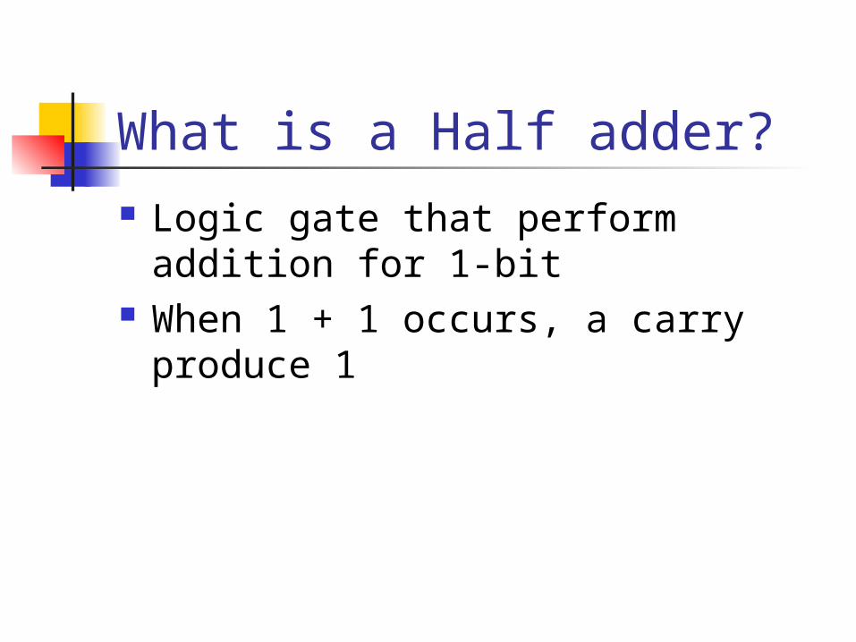
What is a Half adder? Logic gate that perform addition
for 1-bit When 1 + 1 occurs, a carry
produce 1

Half Adder Perform arithmetic additions two inputs A, B to half-adder. Resultants are
Sum(S) and Carry(Cout)
Using K-Map to simplify the sum term, we get
H.AA
B Cout
S
A B S C
0 0 0 0
0 1 1 0
1 0 1 0
1 1 0 1ABC
BA
BABAS
AB
Cout
S

Full Adder

What is Full Adder? A full adder is a circuit that computes the
sum of three bits and gives a two-bit answer. A circuit for adding two 16-bit numbers can
be built from 16 full-adder circuits. Each full-adder does one column of the sum.
The full adder for a given column adds two bits from the input numbers together with a one-bit carry from the previous column to the right. The adder produces a two-bit answer; one of these bits is used as a carry into the next column.

Full Adder A full adder has 3 inputs and 2 outputs The truth table of the full-adder can be
drawn with inputs A,B and Cin with outputs S and Cout From the truth table we can write the Boolean equation
for the S and Cout
Simplify using Boolean Algebra and K-map, we get
FullAdder
A
B
C in
S
C out
ininininout
inininin
ABCCABCBABCAC
ABCCBACBACBAS
ABBCACC
CBAS
ininout
in
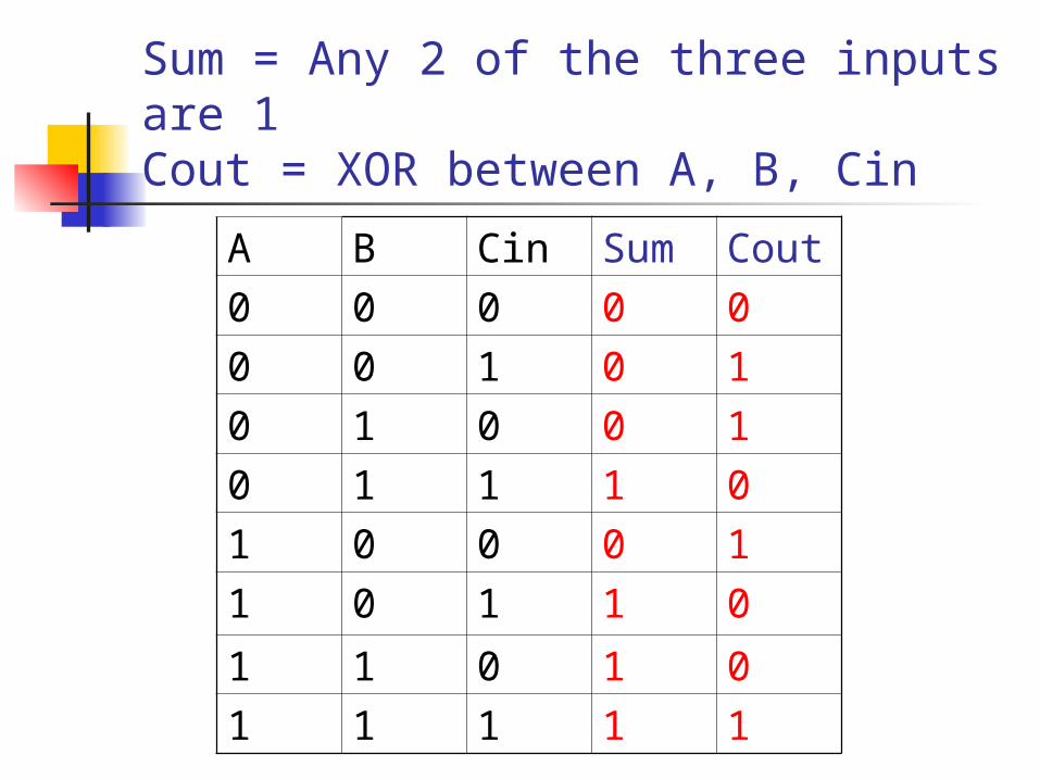
Sum = Any 2 of the three inputs are 1Cout = XOR between A, B, Cin
A B Cin Sum Cout
0 0 0 0 0
0 0 1 0 1
0 1 0 0 1
0 1 1 1 0
1 0 0 0 1
1 0 1 1 0
1 1 0 1 0
1 1 1 1 1

Full Adder diagram

Half Subtractor
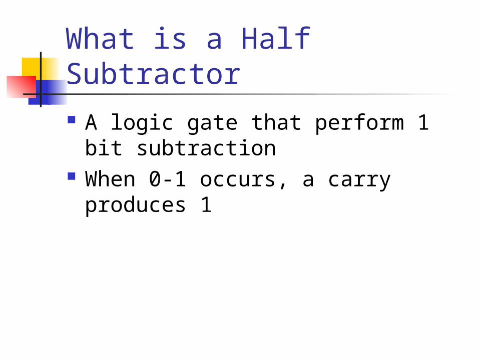
What is a Half Subtractor A logic gate that perform 1 bit
subtraction When 0-1 occurs, a carry produces
1
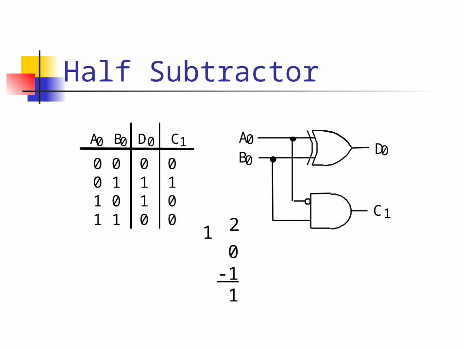
Half Subtractor
C A B D 0 0 0 1
0 0 0 00 1 1 11 0 1 01 1 0 0
A 0 B 0
D 0
C 1
0-1 1
21
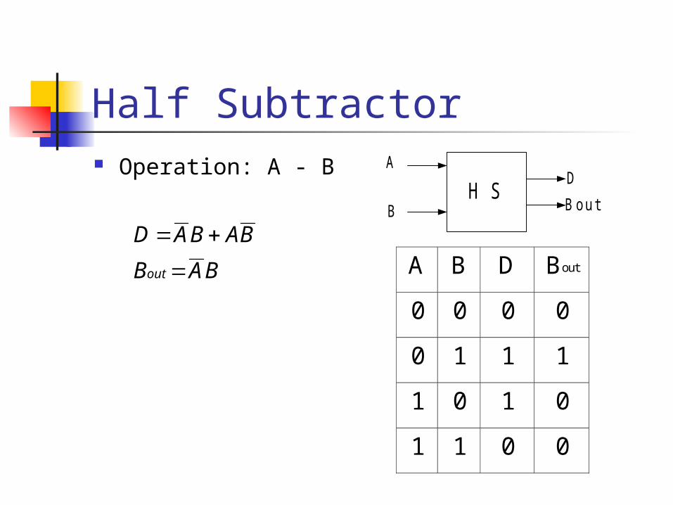
Half Subtractor Operation: A - B
H SA
B
D
Bout
A B D Bout
0 0 0 0
0 1 1 1
1 0 1 0
1 1 0 0
BAB
BABAD
out
Full Subtractor

What is a Full Subtraction? Logic gates that perform two bits
subtraction

Full Subtractor
0 0 0 0 00 0 1 1 10 1 0 1 00 1 1 0 01 0 0 1 11 0 1 0 11 1 0 0 01 1 1 1 1
Ci Ai Bi Di Ci+1
1 1
1 1
Ci
AiBi00 01 11 10
0
1
Di
Di = Ci $ (Ai $ Bi)
Same as Si in full adder

Full Subtractor
0 0 0 0 00 0 1 1 10 1 0 1 00 1 1 0 01 0 0 1 11 0 1 0 11 1 0 0 01 1 1 1 1
Ci Ai Bi Di Ci+1 Ci
AiBi00 01 11 10
0
1
1
1 11
Ci+1
Ci+1 = !Ai & Bi
# Ci & !Ai & !Bi
# Ci & Ai & Bi
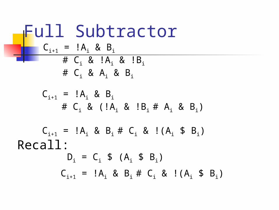
Full SubtractorCi+1 = !Ai & Bi
# Ci & !Ai & !Bi
# Ci & Ai & Bi
Ci+1 = !Ai & Bi
# Ci & (!Ai & !Bi # Ai & Bi)
Ci+1 = !Ai & Bi # Ci & !(Ai $ Bi)
Recall:Di = Ci $ (Ai $ Bi)
Ci+1 = !Ai & Bi # Ci & !(Ai $ Bi)

Full Subtractor
A
B
D
C
C i+1
i
i
i
i
Di = Ci $ (Ai $ Bi)
Ci+1 = !Ai & Bi # Ci & !(Ai $ Bi)
half subtractorhalf subtractor

Full Subtractor Operation: A - B - Bin
F SA
BD
BoutB in
A B Bin D Bout
0 0 0 0 0
0 0 1 1 1
0 1 0 1 1
0 1 1 0 1
1 0 0 1 0
1 0 1 0 0
1 1 0 0 0
1 1 1 1 1
ininout
inininin
BBBABAB
BBAABBBBABBAD

Adder/Subtractor - 1A 0 B 0
D 0
C 1
A 0 B 0
S 0
C 1
A 0
B 0 0
CB1 E
SD
Half adder Half subtractor
E = 0: Half adder
E = 1: Half subtractor

Adder/Subtractor-1
i+1
A B
D
C
C
i i
i
i
E
E = 0: Full adderE = 1: Full subtractor
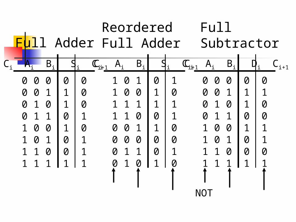
0 0 0 0 00 0 1 1 00 1 0 1 00 1 1 0 11 0 0 1 01 0 1 0 11 1 0 0 11 1 1 1 1
Ci Ai Bi Si Ci+1
1 0 1 0 11 0 0 1 01 1 1 1 11 1 0 0 10 0 1 1 00 0 0 0 00 1 1 0 10 1 0 1 0
Ci Ai Bi Si Ci+1
Full AdderReorderedFull Adder
0 0 0 0 00 0 1 1 10 1 0 1 00 1 1 0 01 0 0 1 11 0 1 0 11 1 0 0 01 1 1 1 1
Ci Ai Bi Di Ci+1
FullSubtractor
NOT

Making a full subtractor from a full adder
Full Adder
A B
C C
D
i i
i+1 i
i

Four-Bit Parallel Adder
This circuit is sometimes referred to as a ripple-through adder
C0 ripples through four two-level logic circuits and hence the sum cannot be completed until eight gate delays
For this kind of adder, the maximum delay is directly proportional to the number of stages n.
F.A 3
A 3 B 3
S 3
C arryO ut
F .A 2
A 2 B 2
S 2
C 3C 2
F.A 1
A 1 B 1
S 1
C 2
F.A 0
A 0 B 0
S 0
C 0

Adder/Subtractor-2
Full Adder
A B
C
0 0
1
0
Full Adder
A B
C
1 1
2
1
Full Adder
A B
C
2 2
3
2
Full Adder
A B
C SD
3 3
4 3 SD SD SD
E
E = 0: 4-bit adderE = 1: 4-bit subtractor

Carry Look-Ahead Circuit To improve the speed of addition Consider the carry output equation for a full
adder is
Which can be expressed as follows
or as where
ininininout ABCCABCBABCAC
ABCBAC inout )(
GPCC inout
ABG
BAP

Carry Look-Ahead Circuit Four a four-bit adder the generate and
propagate terms for each stage are
while the carries for the various stages are333 333
222 222
111 111
000 000
BAPBAG
BAPBAG
BAPBAG
BAPBAG
3 233
2 122
1 011
0 100
GCPC
GCPC
GCPC
GCPC
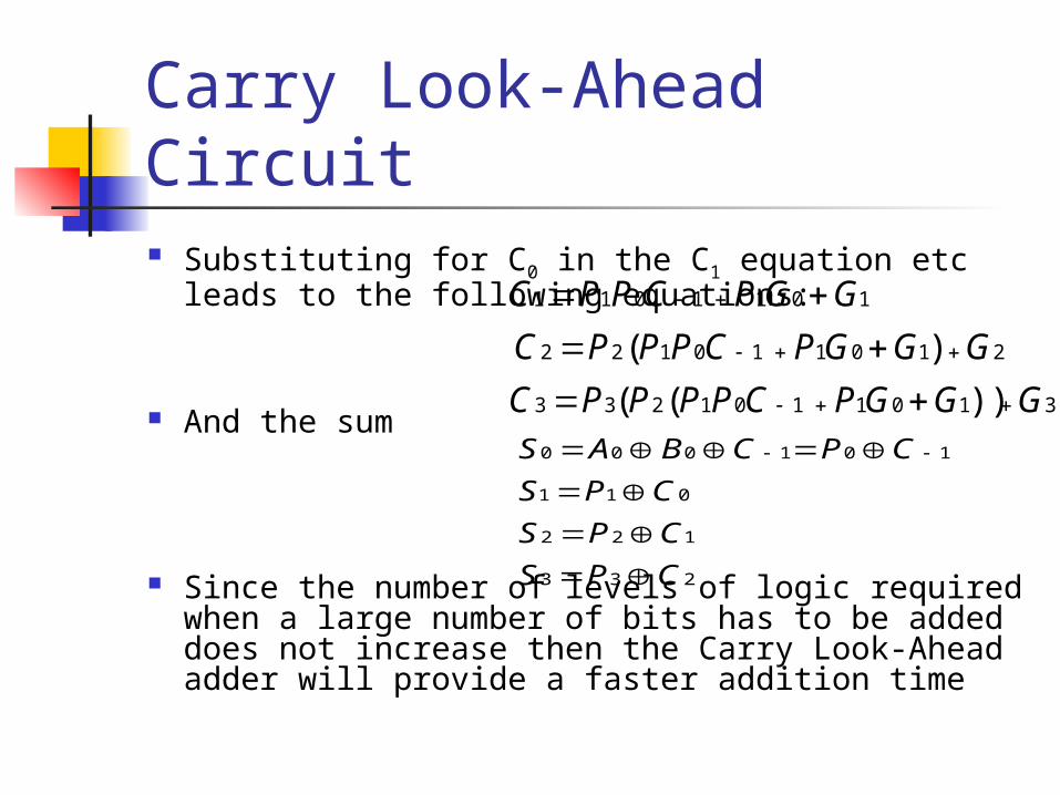
Carry Look-Ahead Circuit Substituting for C0 in the C1 equation etc leads to
the following equations:
And the sum
Since the number of levels of logic required when a large number of bits has to be added does not increase then the Carry Look-Ahead adder will provide a faster addition time
3 101 101 233
2 101 101 22
101 1011
))((
)(
GGGPCPPPPC
GGGPCPPPC
GGPCPPC
233
122
011
10 1000
CPS
CPS
CPS
CPCBAS

Binary Multiplication Paper and Pen method
which is implemented using 9 AND gates, 3 FA and3 HA
0 1 2 3 4 5
1 2 3 4
2 3
20 21 22
10 11 12
00 01 02
0 1 2
0 1 2
PPPPPP
CCCC
CC
BABABA
BABABA
BABABA
BBB
AAA