LMV771 Low Offset, Low Noise, RRO Operational Amplifier in ...
15
LMV771 Low Offset, Low Noise, RRO Operational Amplifier in SC70-5 General Description The LMV771 is a low noise and low cost precision opera- tional amplifier intended for use in a wide range of applica- tions. Other important characteristics of the device include extended operating temperature range, -40˚C to 125˚C, tiny SC70-5 package, and low input bias current. The LMV771 is designed for precision, low noise, low volt- age, and miniature systems. It provides rail-to-rail output swing into heavy loads. The maximum input offset voltage is 850μV at room temperature and the input common mode voltage range includes ground. The LMV771 is offered in the space saving SC70-5 package. Features (Typical 2.7V Supply Values; Unless Otherwise Noted) n Guaranteed 2.7V and 5V specifications n Maximum V OS 850μV (limit) n Voltage noise (1kHz) 9nV/ n Rail-to-Rail output swing — w/600Ω load 100mV from rail — w/2kΩ load 50mV from rail n Silicon Dust™, SC70-5 package 2.0x2.0x1.0mm n Open loop gain w/2kΩ load 100dB n V CM 0 to V + -0.9V n Supply current 550μA n Gain bandwidth product 3.5MHz n Temperature range -40˚C to 125˚C Applications n Transducer amplifier n Instrumentation amplifier n Precision current sensing n Data acquisition systems n Active filters and buffers n Sample and hold n Portable/battery powered electronics Connection Diagram SC70-5 20039667 Top View Instrumentation Amplifier 20039636 January 2003 LMV771 Low Offset, Low Noise, RRO Operational Amplifier in SC70-5 © 2003 National Semiconductor Corporation DS200396 www.national.com
Transcript of LMV771 Low Offset, Low Noise, RRO Operational Amplifier in ...

LMV771Low Offset, Low Noise, RRO Operational Amplifier inSC70-5General DescriptionThe LMV771 is a low noise and low cost precision opera-tional amplifier intended for use in a wide range of applica-tions. Other important characteristics of the device includeextended operating temperature range, −40˚C to 125˚C, tinySC70-5 package, and low input bias current.
The LMV771 is designed for precision, low noise, low volt-age, and miniature systems. It provides rail-to-rail outputswing into heavy loads. The maximum input offset voltage is850µV at room temperature and the input common modevoltage range includes ground.
The LMV771 is offered in the space saving SC70-5 package.
Features(Typical 2.7V Supply Values; Unless Otherwise Noted)n Guaranteed 2.7V and 5V specificationsn Maximum VOS 850µV (limit)n Voltage noise (1kHz) 9nV/n Rail-to-Rail output swing
— w/600Ω load 100mV from rail— w/2kΩ load 50mV from rail
n Silicon Dust™, SC70-5 package 2.0x2.0x1.0mmn Open loop gain w/2kΩ load 100dBn VCM 0 to V+ -0.9Vn Supply current 550µAn Gain bandwidth product 3.5MHzn Temperature range −40˚C to 125˚C
Applicationsn Transducer amplifiern Instrumentation amplifiern Precision current sensingn Data acquisition systemsn Active filters and buffersn Sample and holdn Portable/battery powered electronics
Connection DiagramSC70-5
20039667
Top View
Instrumentation Amplifier
20039636
January 2003LM
V771
LowO
ffset,LowN
oise,RR
OO
perationalAm
plifierin
SC
70-5
© 2003 National Semiconductor Corporation DS200396 www.national.com

Absolute Maximum Ratings (Note 1)
If Military/Aerospace specified devices are required,please contact the National Semiconductor Sales Office/Distributors for availability and specifications.
ESD Tolerance (Note 2)
Machine Model 200V
Human Body Model 2000V
Differential Input Voltage ± Supply Voltage
Supply Voltage (V+–V −) 6.5V
Output Short Circuit to V+ (Note 3)
Output Short Circuit to V− (Note 4)
Storage Temperature Range −65˚C to 150˚C
Junction Temperature (Note 5) 150˚C
Mounting Temp.
Infrared or Convection (20 sec) 235˚C
Wave Soldering Lead Temp (10sec) 260˚C
Operating Ratings (Note 1)
Temperature Range −40˚C to 125˚C
Thermal Resistance (θJA)
SC70-5 Package 440 ˚C/W
2.7V DC Electrical Characteristics (Note 10)
Unless otherwise specified, all limits guaranteed for TJ = 25˚C. V+ = 2.7V, V − = 0V, VCM = V+/2, VO = V+/2 andRL > 1MΩ. Boldface limits apply at the temperature extremes.
Symbol Parameter Condition Min(Note 7)
Typ(Note 6)
Max(Note 7)
Units
VOS Input Offset Voltage 0.30 0.851.0
mV
TCVOS Input Offset Voltage AverageDrift
−0.45 µV/˚C
IB Input Bias Current −0.1 100 pA
IOS Input Offset Current 0.004 100 pA
IS Supply Current 550 900910
µA
CMRR Common Mode Rejection Ratio 0.5 ≤ VCM ≤ 1.2V 7472
80dB
PSRR Power Supply Rejection Ratio 2.7V ≤ V+ ≤ 5V 8276
90 dB
VCM Input Common-Mode VoltageRange
For CMRR ≥ 50dB 0 1.8 V
AV Large Signal Voltage Gain(Note 8)
RL = 600Ω to 1.35V,VO = 0.2V to 2.5V
9280
100
dBRL = 2kΩ to 1.35V,VO = 0.2V to 2.5V
9886
100
VO Output Swing RL = 600Ω to 1.35VVIN = ± 100mV
0.110.14
0.084 to2.62
2.592.56
VRL = 2kΩ to 1.35VVIN = ± 100mV
0.050.06
0.026 to2.68
2.652.64
IO Output Short Circuit Current Sourcing, VO = 0VVIN = 100mV
1811
24
mASinking, VO = 2.7VVIN = −100mV
1811
22
2.7V AC Electrical CharacteristicsUnless otherwise specified, all limits guaranteed for TJ = 25˚C. V+ = 5.0V, V − = 0V, VCM = V+/2, VO = V+/2 and RL > 1MΩ.Boldface limits apply at the temperature extremes.
Symbol Parameter Conditions Min(Note 7)
Typ(Note 6)
Max(Note 7)
Units
SR Slew Rate (Note 9) 1.4 V/µs
GBW Gain-Bandwidth Product 3.5 MHz
Φm Phase Margin 79 Deg
LMV
771
www.national.com 2

2.7V AC Electrical Characteristics (Continued)Unless otherwise specified, all limits guaranteed for TJ = 25˚C. V+ = 5.0V, V − = 0V, VCM = V+/2, VO = V+/2 and RL > 1MΩ.Boldface limits apply at the temperature extremes.
Symbol Parameter Conditions Min(Note 7)
Typ(Note 6)
Max(Note 7)
Units
Gm Gain Margin −15 dB
en Input-Referred Voltage Noise(Flatband)
f = 10KHz 7.5 nV/
en Input-Referred Voltage Noise(l/f)
f = 100Hz 17 nV/
in Input-Referred Current Noise f = 1kHz 0.001 pA/
THD Total Harmonic Distortion f = 1kHz, AV = +1RL = 600Ω, VIN = 1 VPP
0.007 %
5.0V DC Electrical CharacteristicsUnless otherwise specified, all limits guaranteed for TJ = 25˚C. V+ = 5.0V, V − = 0V, VCM = V+/2, VO = V+/2 andRL > 1MΩ. Boldface limits apply at the temperature extremes.
Symbol Parameter Condition Min(Note7)
Typ(Note 6)
Max(Note 7)
Units
VOS Input Offset Voltage 0.25 0.851.0
mV
TCVOS Input Offset Voltage AverageDrift
−0.35 µV/˚C
IB Input Bias Current −0.23 100 pA
IOS Input Offset Current 0.017 100 pA
IS Supply Current 600 950960
µA
CMRR Common Mode Rejection Ratio 0.5 ≤ VCM ≤ 3.5V 8079
90dB
PSRR Power Supply Rejection Ratio 2.7V ≤ V+ ≤ 5V 8276
90 dB
VCM Input Common-Mode VoltageRange
For CMRR ≥ 50dB 0 4.1 V
AV Large Signal Voltage Gain(Note 8)
RL = 600Ω to 2.5V,VO = 0.2V to 4.8V
9289
100
dBRL = 2kΩ to 2.5V,VO = 0.2V to 4.8V
9895
100
VO Output Swing RL = 600Ω to 2.5VVIN = ± 100mV
0.150.23
0.112 to4.9
4.854.77
VRL = 2kΩ to 2.5VVIN = ± 100mV
0.060.07
0.035 to4.97
4.944.93
IO Output Short Circuit Current Sourcing, VO = 0VVIN = 100mV
3535
75
mASinking, VO = 2.7VVIN = −100mV
3535
66
5.0V AC Electrical CharacteristicsUnless otherwise specified, all limits guaranteed for TJ = 25˚C. V+ = 5.0V, V − = 0V, VCM = V+/2, VO = V+/2 and RL > 1MΩ.Boldface limits apply at the temperature extremes.
Symbol Parameter Conditions Min(Note 7)
Typ(Note 6)
Max(Note 7)
Units
SR Slew Rate (Note 9) 1.4 V/µs
LMV
771
www.national.com3

5.0V AC Electrical Characteristics (Continued)Unless otherwise specified, all limits guaranteed for TJ = 25˚C. V+ = 5.0V, V − = 0V, VCM = V+/2, VO = V+/2 and RL > 1MΩ.Boldface limits apply at the temperature extremes.
Symbol Parameter Conditions Min(Note 7)
Typ(Note 6)
Max(Note 7)
Units
GBW Gain-Bandwidth Product 3.5 MHz
Φm Phase Margin 79 Deg
Gm Gain Margin −15 dB
en Input-Referred Voltage Noise(Flatband)
f = 10KHz 6.5 nV/
en Input-Referred Voltage Noise(l/f)
f = 100Hz 12 nV/
in Input-Referred Current Noise f = 1kHz 0.001 pA/
THD Total Harmonic Distortion f = 1kHz, AV = +1RL = 600Ω, VIN = 1 VPP
0.007 %
Note 1: Absolute Maximum Ratings indicate limits beyond which damage to the device may occur. Operating Ratings indicate conditions for which the device isintended to be functional, but specific performance is not guaranteed. For guaranteed specifications and the test conditions, see the Electrical Characteristics.
Note 2: Human body model, 1.5kΩ in series with 100pF. Machine model, 0Ω in series with 20pF.
Note 3: Shorting output to V+ will adversely affect reliability.
Note 4: Shorting output to V− will adversely affect reliability.
Note 5: The maximum power dissipation is a function of TJ(MAX) , θJA, and TA. The maximum allowable power dissipation at any ambient temperature isPD = (TJ(MAX)–T A)/θJA. All numbers apply for packages soldered directly into a PC board.
Note 6: Typical Values represent the most likely parametric norm.
Note 7: All limits are guaranteed by testing or statistical analysis.
Note 8: RL is connected to mid-supply. The output voltage is set at 200mV from the rails. VO = GND+0.2V and VO = V+ −0.2V
Note 9: Connected as Voltage follower with 2VPP step input. Number Specified is the slower of positive and negative slew Rates.
Note 10: Electrical Table values apply only for factory testing conditions at the temperature indicated. Factory testing conditions result in very limited self-heatingof the device such that TJ = TA . No guarantee of parametric performance is indicated in the electrical tables under the conditions of internal self-heating where TJ> TA. Absolute Maximum Rating indicated junction temperature limits beyond which the device may be permanently degraded, either mechanically or electrically.
Note 11: Continuous operation of the device with an output short circuit current larger than 35mA may cause permanent damage to the device.
Ordering Information
Package Part Number Package Marking Transport Media NSC Drawing
SC70-5 LMV771MG A75 1k Units Tape and Reel MAA05A
LMV771MGX 3k Units Tape and Reel
LMV
771
www.national.com 4
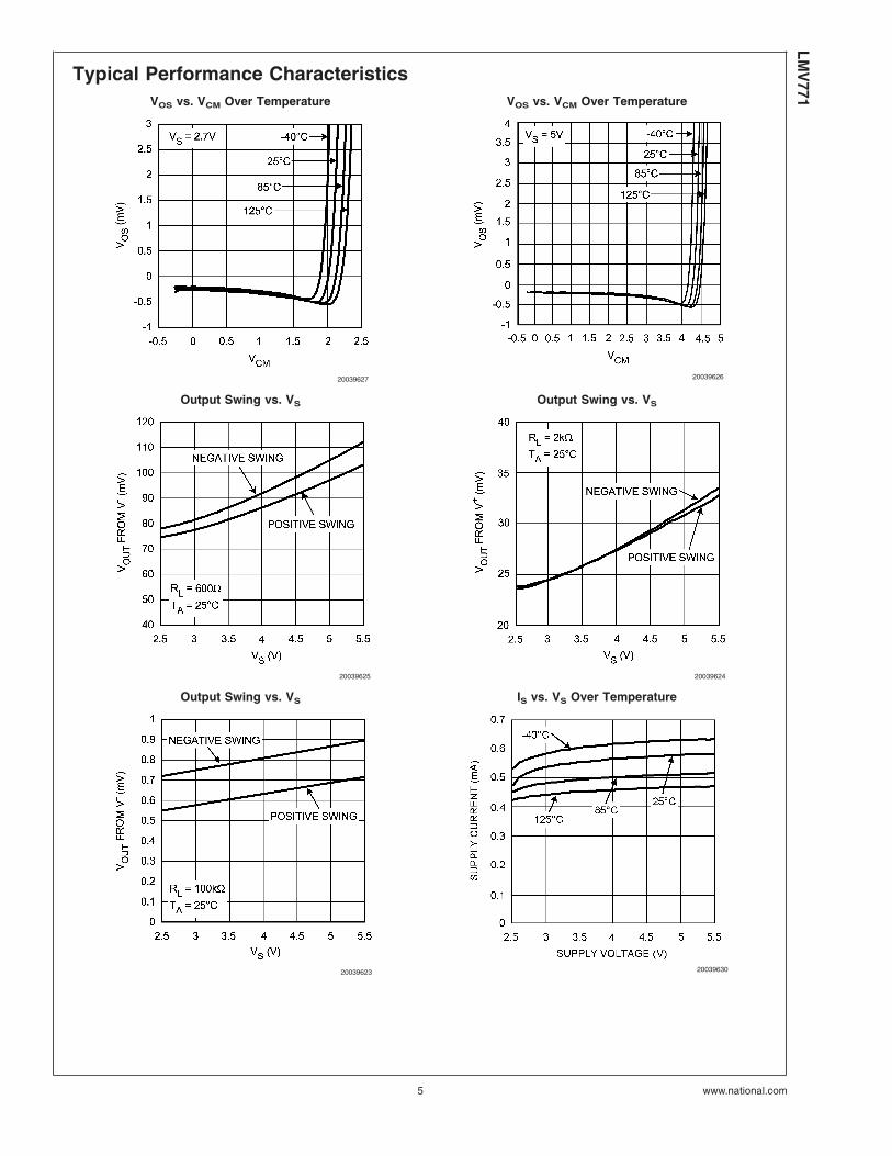
Typical Performance CharacteristicsVOS vs. VCM Over Temperature VOS vs. VCM Over Temperature
20039627 20039626
Output Swing vs. VS Output Swing vs. VS
20039625 20039624
Output Swing vs. VS IS vs. VS Over Temperature
20039623 20039630
LMV
771
www.national.com5
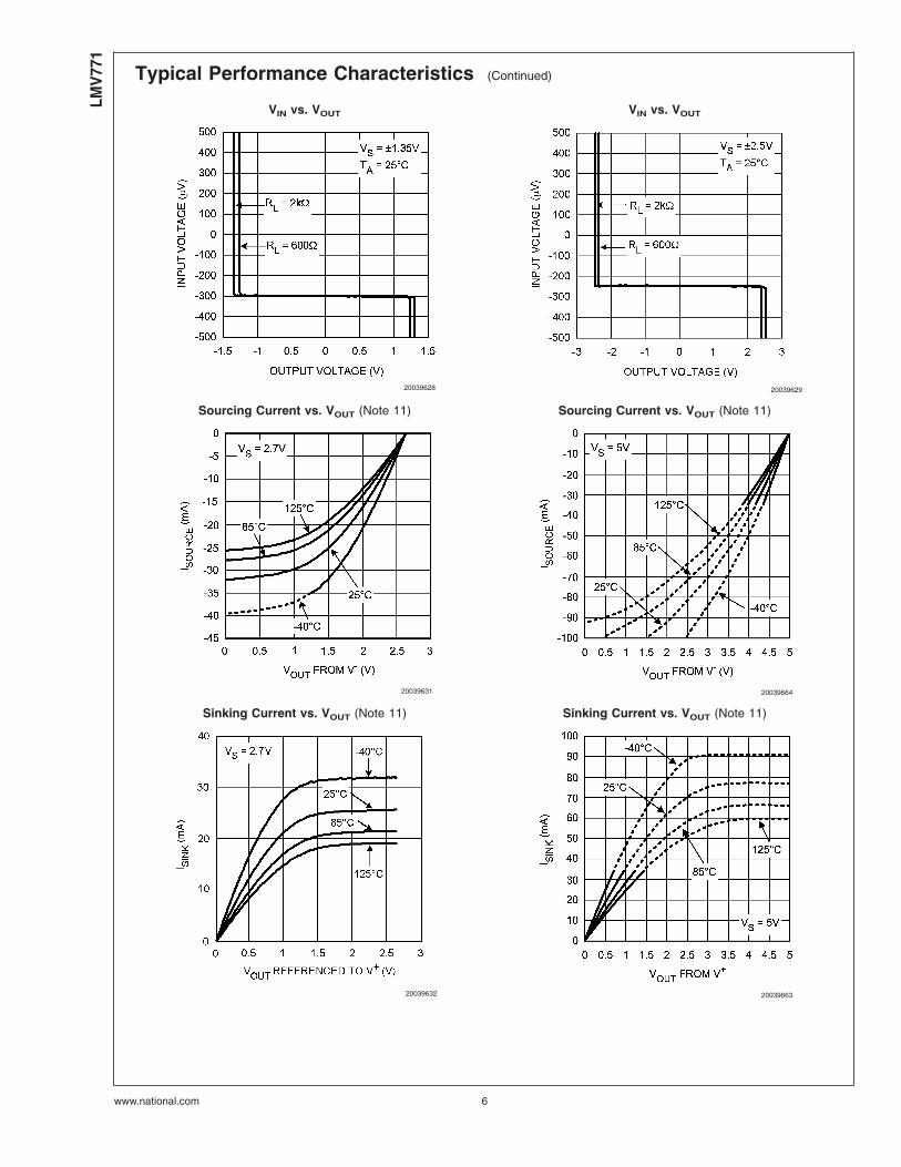
Typical Performance Characteristics (Continued)
VIN vs. VOUT VIN vs. VOUT
20039628 20039629
Sourcing Current vs. VOUT (Note 11) Sourcing Current vs. VOUT (Note 11)
20039631 20039664
Sinking Current vs. VOUT (Note 11) Sinking Current vs. VOUT (Note 11)
20039632 20039663
LMV
771
www.national.com 6

Typical Performance Characteristics (Continued)
Input Voltage Noise vs. Frequency Input Bias Current Over Temperature
20039608 20039635
Input Bias Current Over Temperature Input Bias Current Over Temperature
20039634 20039633
THD+N vs. Frequency THD+N vs. VOUT
2003960720039666
LMV
771
www.national.com7

Typical Performance Characteristics (Continued)
Slew Rate vs. Supply Voltage Open Loop Frequency Response Over Temperature
20039601 20039602
Open Loop Frequency Response Open Loop Frequency Response
20039603 20039604
Open Loop Gain & Phase with Cap. Loading Open Loop Gain & Phase with Cap. Loading
20039605 20039606
LMV
771
www.national.com 8
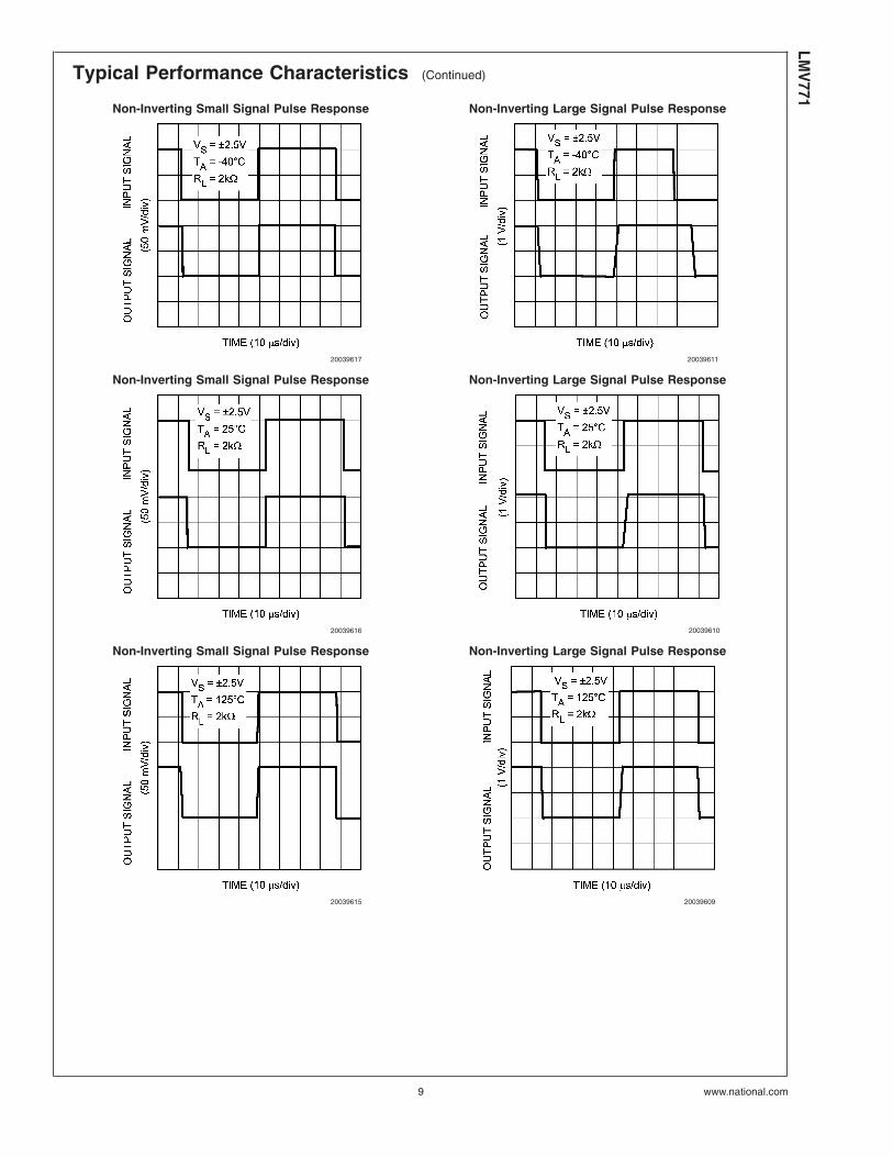
Typical Performance Characteristics (Continued)
Non-Inverting Small Signal Pulse Response Non-Inverting Large Signal Pulse Response
20039617 20039611
Non-Inverting Small Signal Pulse Response Non-Inverting Large Signal Pulse Response
20039616 20039610
Non-Inverting Small Signal Pulse Response Non-Inverting Large Signal Pulse Response
20039615 20039609
LMV
771
www.national.com9

Typical Performance Characteristics (Continued)
Inverting Small Signal Pulse Response Inverting Large Signal Pulse Response
20039619 20039614
Inverting Small Signal Pulse Response Inverting Large Signal Pulse Response
20039620 20039613
Inverting Small Signal Pulse Response Inverting Large Signal Pulse Response
20039618 20039612
LMV
771
www.national.com 10

Typical Performance Characteristics (Continued)
Stability vs. VCM Stability vs. VCM
20039621 20039622
PSRR vs. Frequency CMRR vs. Frequency
20039668 20039665
LMV
771
www.national.com11
Application Note
LMV771
The LMV771 is a single, low cost precision amplifier withvery low noise and ultra low offset voltage.
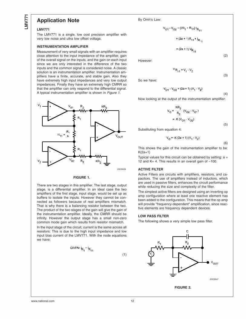
INSTRUMENTATION AMPLIFIER
Measurement of very small signals with an amplifier requiresclose attention to the input impedance of the amplifier, gainof the overall signal on the inputs, and the gain on each inputsince we are only interested in the difference of the twoinputs and the common signal is considered noise. A classicsolution is an instrumentation amplifier. Instrumentation am-plifiers have a finite, accurate, and stable gain. Also theyhave extremely high input impedances and very low outputimpedances. Finally they have an extremely high CMRR sothat the amplifier can only respond to the differential signal.A typical instrumentation amplifier is shown in Figure 1.
There are two stages in this amplifier. The last stage, outputstage, is a differential amplifier. In an ideal case the twoamplifiers of the first stage, input stage, would be set up asbuffers to isolate the inputs. However they cannot be con-nected as followers because of real amplifiers mismatch.That is why there is a balancing resistor between the two.The product of the two stages of the gain will give the gain ofthe instrumentation amplifier. Ideally, the CMRR should beinfinity. However the output stage has a small non-zerocommon mode gain which results from resistor mismatch.
In the input stage of the circuit, current is the same across allresistors. This is due to the high input impedance and lowinput bias current of the LMV771. With the node equationswe have:
(1)
By Omh’s Law:
(2)
However:
(3)
So we have:
(4)
Now looking at the output of the instrumentation amplifier:
(5)
Substituting from equation 4:
(6)
This shows the gain of the instrumentation amplifier to be:K(2a+1)
Typical values for this circuit can be obtained by setting: a =12 and K= 4. This results in an overall gain of −100.
ACTIVE FILTER
Active Filters are circuits with amplifiers, resistors, and ca-pacitors. The use of amplifiers instead of inductors, whichare used in passive filters, enhances the circuit performancewhile reducing the size and complexity of the filter.
The simplest active filters are designed using an inverting opamp configuration where at least one reactive element hasbeen added to the configuration. This means that the op ampwill provide "frequency-dependent" amplification, since reac-tive elements are frequency dependent devices.
LOW PASS FILTER
The following shows a very simple low pass filter.
20039636
FIGURE 1.
20039647
FIGURE 2.
LMV
771
www.national.com 12

Application Note (Continued)
The transfer function can be expressed as follows:
By KCL:
(7)
Simplifying this further results in:
(8)
or
(9)
Now, substituting ω=2πf, so that the calculations are in f(Hz)and not ω(rad/s), and setting the DC gain and
(10)
Set:
(11)
Low pass filters are known as lossy integrators because theyonly behave as an integrator at higher frequencies. Just bylooking at the transfer function one can predict the generalform of the bode plot. When the f/fO ratio is small, thecapacitor is in effect an open circuit and the amplifier be-haves at a set DC gain. Starting at fO, −3dB corner, thecapacitor will have the dominant impedance and hence thecircuit will behave as an integrator and the signal will beattenuated and eventually cut. The bode plot for this filter isshown in the following picture:
HIGH PASS FILTER
In a similar approach, one can derive the transfer function ofa high pass filter. A typical first order high pass filter is shownbelow:
Writing the KCL for this circuit :
(V1 denotes the voltage between C and R1)
(12)
(13)
Solving these two equations to find the transfer function andusing:
(high frequency gain) and
Which results:
(14)
Looking at the transfer function, it is clear that when f/fO issmall, the capacitor is open and hence no signal is getting into the amplifier. As the frequency increases the amplifierstarts operating. At f = fO the capacitor behaves like a shortcircuit and the amplifier will have a constant, high frequency,gain of HO. The bode plot of the transfer function follows:
20039653
FIGURE 3.
20039654
FIGURE 4.
LMV
771
www.national.com13

Application Note (Continued)
BAND PASS FILTER
Combining a low pass filter and a high pass filter will gener-ate a band pass filter. In this network the input impedance
forms the high pass filter while the feedback impedanceforms the low pass filter. Choosing the corner frequencies sothat f1 < f2, then all the frequencies in between, f1 ≤ f ≤ f2, willpass through the filter while frequencies below f1 and abovef2 will be cut off.
The transfer function can be easily calculated using thesame methodology as before.
(15)
Where
The transfer function is presented in the following figure.
20039658
FIGURE 5.
20039660
FIGURE 6.20039662
FIGURE 7.
LMV
771
www.national.com 14

Physical Dimensions inches (millimeters)unless otherwise noted
SC70-5NS Package Number MAA05A
LIFE SUPPORT POLICY
NATIONAL’S PRODUCTS ARE NOT AUTHORIZED FOR USE AS CRITICAL COMPONENTS IN LIFE SUPPORTDEVICES OR SYSTEMS WITHOUT THE EXPRESS WRITTEN APPROVAL OF THE PRESIDENT AND GENERALCOUNSEL OF NATIONAL SEMICONDUCTOR CORPORATION. As used herein:
1. Life support devices or systems are devices orsystems which, (a) are intended for surgical implantinto the body, or (b) support or sustain life, andwhose failure to perform when properly used inaccordance with instructions for use provided in thelabeling, can be reasonably expected to result in asignificant injury to the user.
2. A critical component is any component of a lifesupport device or system whose failure to performcan be reasonably expected to cause the failure ofthe life support device or system, or to affect itssafety or effectiveness.
National SemiconductorAmericas CustomerSupport CenterEmail: [email protected]: 1-800-272-9959
National SemiconductorEurope Customer Support Center
Fax: +49 (0) 180-530 85 86Email: [email protected]
Deutsch Tel: +49 (0) 69 9508 6208English Tel: +44 (0) 870 24 0 2171Français Tel: +33 (0) 1 41 91 8790
National SemiconductorAsia Pacific CustomerSupport CenterFax: 65-6250 4466Email: [email protected]: 65-6254 4466
National SemiconductorJapan Customer Support CenterFax: 81-3-5639-7507Email: [email protected]: 81-3-5639-7560
www.national.com
LMV
771Low
Offset,Low
Noise,R
RO
OperationalA
mplifier
inS
C70-5
National does not assume any responsibility for use of any circuitry described, no circuit patent licenses are implied and National reserves the right at any time without notice to change said circuitry and specifications.