LM3445 Triac Dimmable Offline LED Driver (Rev. K) · LM3445 Triac Dimmable Offline LED Driver....
28
LM3445 LM3445 Triac Dimmable Offline LED Driver Literature Number: SNVS570K
Transcript of LM3445 Triac Dimmable Offline LED Driver (Rev. K) · LM3445 Triac Dimmable Offline LED Driver....
LM3445
LM3445 Triac Dimmable Offline LED Driver
Literature Number: SNVS570K
LM3445
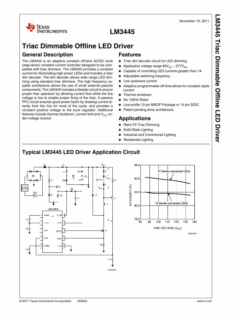
November 10, 2011
Triac Dimmable Offline LED DriverGeneral DescriptionThe LM3445 is an adaptive constant off-time AC/DC buck(step-down) constant current controller designed to be com-patible with triac dimmers. The LM3445 provides a constantcurrent for illuminating high power LEDs and includes a triacdim decoder. The dim decoder allows wide range LED dim-ming using standard triac dimmers. The high frequency ca-pable architecture allows the use of small external passivecomponents. The LM3445 includes a bleeder circuit to ensureproper triac operation by allowing current flow while the linevoltage is low to enable proper firing of the triac. A passivePFC circuit ensures good power factor by drawing current di-rectly from the line for most of the cycle, and provides aconstant positive voltage to the buck regulator. Additionalfeatures include thermal shutdown, current limit and VCC un-der-voltage lockout.
Features Triac dim decoder circuit for LED dimming
Application voltage range 80VAC – 277VAC
Capable of controlling LED currents greater than 1A
Adjustable switching frequency
Low quiescent current
Adaptive programmable off-time allows for constant ripplecurrent
Thermal shutdown
No 120Hz flicker
Low profile 10 pin MSOP Package or 14 pin SOIC
Patent pending drive architecture
Applications Retro Fit Triac Dimming
Solid State Lighting
Industrial and Commercial Lighting
Residential Lighting
Typical LM3445 LED Driver Application Circuit
30060301
30060305
© 2011 Texas Instruments Incorporated 300603 www.ti.com
LM
3445 T
riac D
imm
ab
le O
ffline L
ED
Driv
er
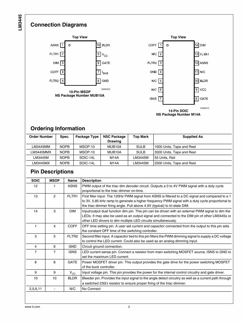
Connection Diagrams
Top View
30060303
10-Pin MSOPNS Package Number MUB10A
Top View
30060373
14-Pin SOICNS Package Number M14A
Ordering Information
Order Number Spec. Package Type NSC Package
Drawing
Top Mark Supplied As
LM3445MM NOPB MSOP-10 MUB10A SULB 1000 Units, Tape and Reel
LM3445MMX NOPB MSOP-10 MUB10A SULB 3500 Units, Tape and Reel
LM3445M NOPB SOIC-14L M14A LM3445M 55 Units, Rail
LM3445MX NOPB SOIC-14L M14A LM3445M 2500 Units, Tape and Reel
Pin Descriptions
SOIC MSOP Name Description
12 1 ASNS PWM output of the triac dim decoder circuit. Outputs a 0 to 4V PWM signal with a duty cycle
proportional to the triac dimmer on-time.
13 2 FLTR1 First filter input. The 120Hz PWM signal from ASNS is filtered to a DC signal and compared to a 1
to 3V, 5.85 kHz ramp to generate a higher frequency PWM signal with a duty cycle proportional to
the triac dimmer firing angle. Pull above 4.9V (typical) to tri-state DIM.
14 3 DIM Input/output dual function dim pin. This pin can be driven with an external PWM signal to dim the
LEDs. It may also be used as an output signal and connected to the DIM pin of other LM3445s or
other LED drivers to dim multiple LED circuits simultaneously.
1 4 COFF OFF time setting pin. A user set current and capacitor connected from the output to this pin sets
the constant OFF time of the switching controller.
3 5 FLTR2 Second filter input. A capacitor tied to this pin filters the PWM dimming signal to supply a DC voltage
to control the LED current. Could also be used as an analog dimming input.
4 6 GND Circuit ground connection.
7 7 ISNS LED current sense pin. Connect a resistor from main switching MOSFET source, ISNS to GND to
set the maximum LED current.
8 8 GATE Power MOSFET driver pin. This output provides the gate drive for the power switching MOSFET
of the buck controller.
9 9 VCC Input voltage pin. This pin provides the power for the internal control circuitry and gate driver.
10 10 BLDR Bleeder pin. Provides the input signal to the angle detect circuitry as well as a current path through
a switched 230Ω resistor to ensure proper firing of the triac dimmer.
2,5,6,11 - N/C No Connect
www.ti.com 2
LM
3445
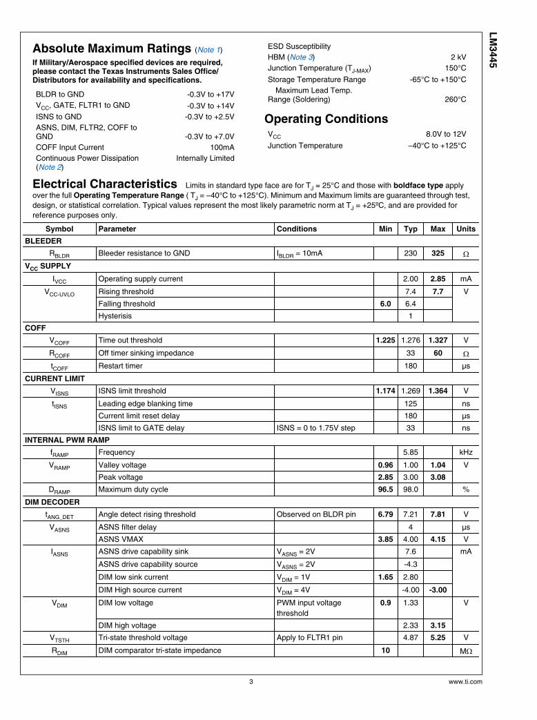
Absolute Maximum Ratings (Note 1)
If Military/Aerospace specified devices are required,please contact the Texas Instruments Sales Office/Distributors for availability and specifications.
BLDR to GND -0.3V to +17V
VCC, GATE, FLTR1 to GND -0.3V to +14V
ISNS to GND -0.3V to +2.5V
ASNS, DIM, FLTR2, COFF toGND -0.3V to +7.0V
COFF Input Current 100mA
Continuous Power Dissipation(Note 2)
Internally Limited
ESD Susceptibility
HBM (Note 3) 2 kV
Junction Temperature (TJ-MAX) 150°C
Storage Temperature Range -65°C to +150°C
Maximum Lead Temp.Range (Soldering) 260°C
Operating ConditionsVCC 8.0V to 12V
Junction Temperature −40°C to +125°C
Electrical Characteristics Limits in standard type face are for TJ = 25°C and those with boldface type apply
over the full Operating Temperature Range ( TJ = −40°C to +125°C). Minimum and Maximum limits are guaranteed through test,
design, or statistical correlation. Typical values represent the most likely parametric norm at TJ = +25ºC, and are provided for
reference purposes only.
Symbol Parameter Conditions Min Typ Max Units
BLEEDER
RBLDR Bleeder resistance to GND IBLDR = 10mA 230 325 ΩVCC SUPPLY
IVCC Operating supply current 2.00 2.85 mA
VCC-UVLO Rising threshold 7.4 7.7 V
Falling threshold 6.0 6.4
Hysterisis 1
COFF
VCOFF Time out threshold 1.225 1.276 1.327 V
RCOFF Off timer sinking impedance 33 60 ΩtCOFF Restart timer 180 µs
CURRENT LIMIT
VISNS ISNS limit threshold 1.174 1.269 1.364 V
tISNS Leading edge blanking time 125 ns
Current limit reset delay 180 µs
ISNS limit to GATE delay ISNS = 0 to 1.75V step 33 ns
INTERNAL PWM RAMP
fRAMP Frequency 5.85 kHz
VRAMP Valley voltage 0.96 1.00 1.04 V
Peak voltage 2.85 3.00 3.08
DRAMP Maximum duty cycle 96.5 98.0 %
DIM DECODER
tANG_DET Angle detect rising threshold Observed on BLDR pin 6.79 7.21 7.81 V
VASNS ASNS filter delay 4 µs
ASNS VMAX 3.85 4.00 4.15 V
IASNS ASNS drive capability sink VASNS = 2V 7.6 mA
ASNS drive capability source VASNS = 2V -4.3
DIM low sink current VDIM = 1V 1.65 2.80
DIM High source current VDIM = 4V -4.00 -3.00
VDIM DIM low voltage PWM input voltage
threshold
0.9 1.33 V
DIM high voltage 2.33 3.15
VTSTH Tri-state threshold voltage Apply to FLTR1 pin 4.87 5.25 V
RDIM DIM comparator tri-state impedance 10 MΩ
3 www.ti.com
LM
3445
Symbol Parameter Conditions Min Typ Max Units
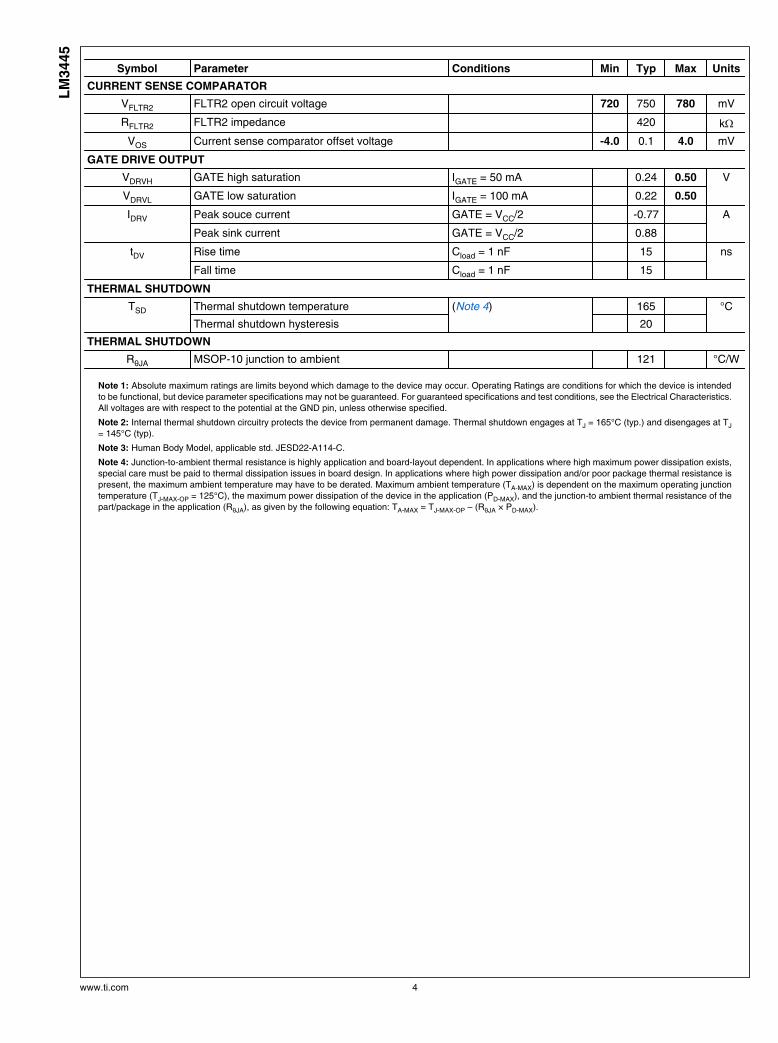
CURRENT SENSE COMPARATOR
VFLTR2 FLTR2 open circuit voltage 720 750 780 mV
RFLTR2 FLTR2 impedance 420 kΩVOS Current sense comparator offset voltage -4.0 0.1 4.0 mV
GATE DRIVE OUTPUT
VDRVH GATE high saturation IGATE = 50 mA 0.24 0.50 V
VDRVL GATE low saturation IGATE = 100 mA 0.22 0.50
IDRV Peak souce current GATE = VCC/2 -0.77 A
Peak sink current GATE = VCC/2 0.88
tDV Rise time Cload = 1 nF 15 ns
Fall time Cload = 1 nF 15
THERMAL SHUTDOWN
TSD Thermal shutdown temperature (Note 4) 165 °C
Thermal shutdown hysteresis 20
THERMAL SHUTDOWN
RθJA MSOP-10 junction to ambient 121 °C/W
Note 1: Absolute maximum ratings are limits beyond which damage to the device may occur. Operating Ratings are conditions for which the device is intendedto be functional, but device parameter specifications may not be guaranteed. For guaranteed specifications and test conditions, see the Electrical Characteristics.All voltages are with respect to the potential at the GND pin, unless otherwise specified.
Note 2: Internal thermal shutdown circuitry protects the device from permanent damage. Thermal shutdown engages at TJ = 165°C (typ.) and disengages at TJ
= 145°C (typ).
Note 3: Human Body Model, applicable std. JESD22-A114-C.
Note 4: Junction-to-ambient thermal resistance is highly application and board-layout dependent. In applications where high maximum power dissipation exists,special care must be paid to thermal dissipation issues in board design. In applications where high power dissipation and/or poor package thermal resistance ispresent, the maximum ambient temperature may have to be derated. Maximum ambient temperature (TA-MAX) is dependent on the maximum operating junctiontemperature (TJ-MAX-OP = 125°C), the maximum power dissipation of the device in the application (PD-MAX), and the junction-to ambient thermal resistance of thepart/package in the application (RθJA), as given by the following equation: TA-MAX = TJ-MAX-OP – (RθJA × PD-MAX).
www.ti.com 4
LM
3445
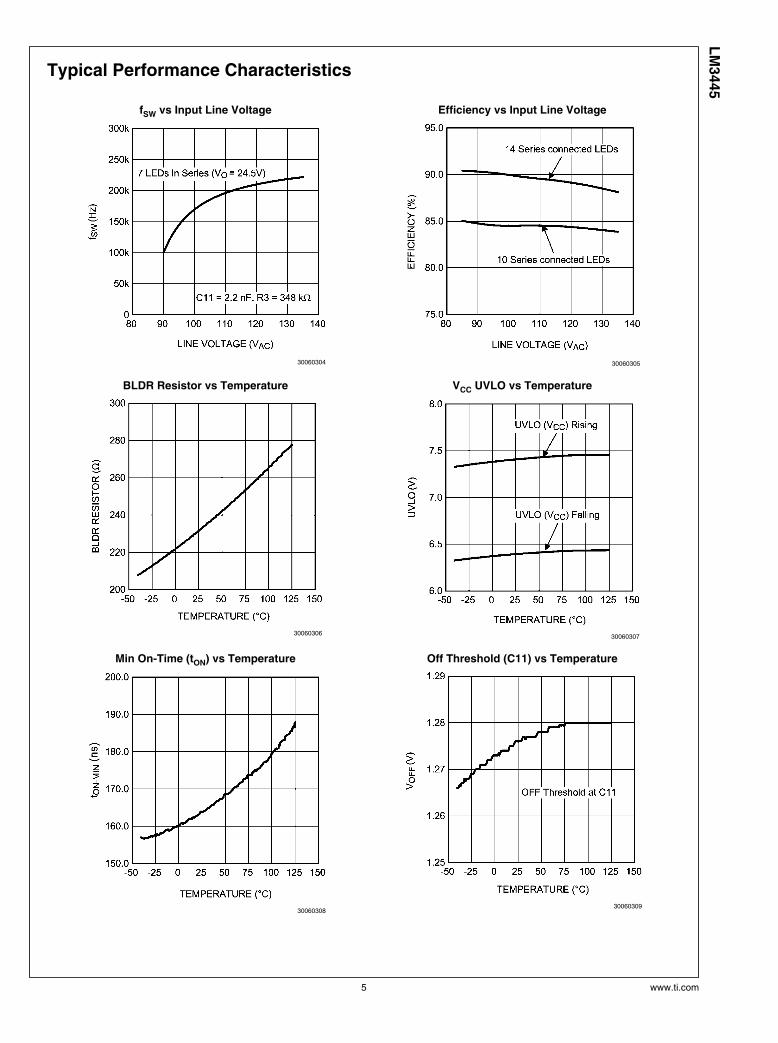
Typical Performance Characteristics
fSW vs Input Line Voltage
30060304
Efficiency vs Input Line Voltage
30060305
BLDR Resistor vs Temperature
30060306
VCC UVLO vs Temperature
30060307
Min On-Time (tON) vs Temperature
30060308
Off Threshold (C11) vs Temperature
30060309
5 www.ti.com
LM
3445
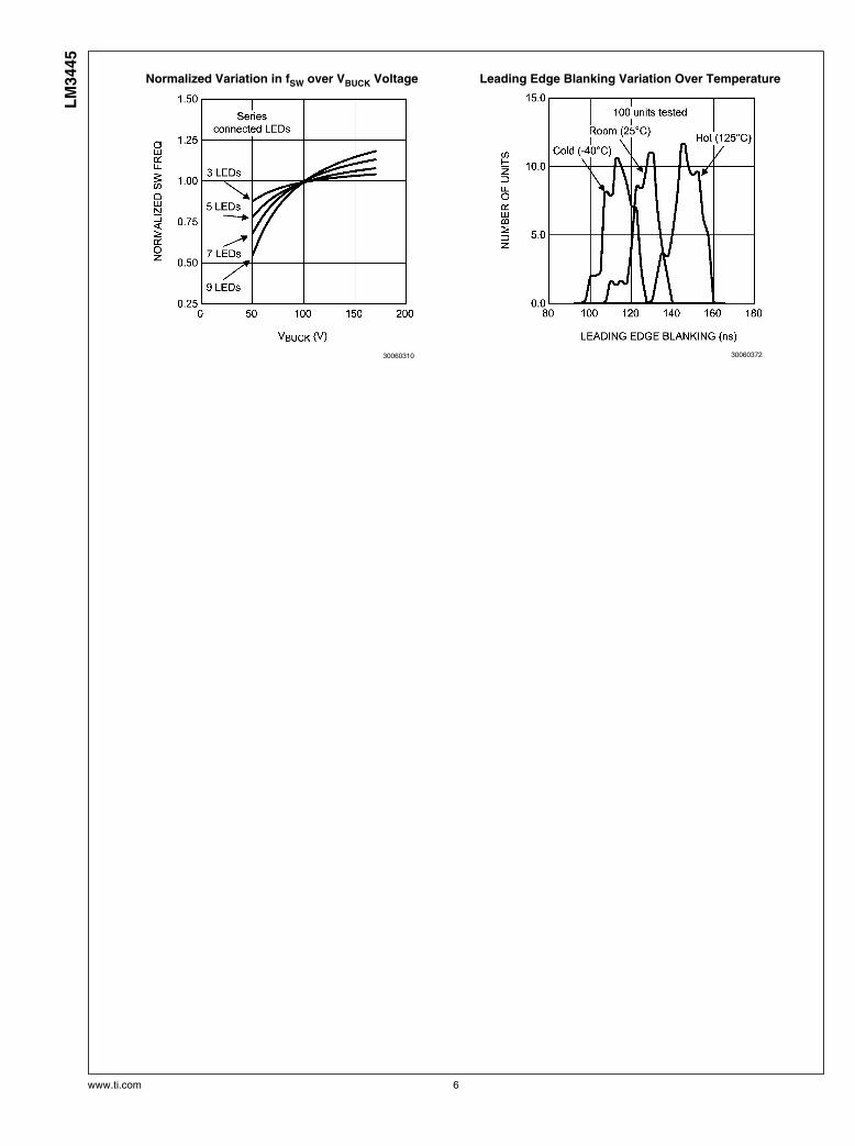
Normalized Variation in fSW over VBUCK Voltage
30060310
Leading Edge Blanking Variation Over Temperature
30060372
www.ti.com 6
LM
3445
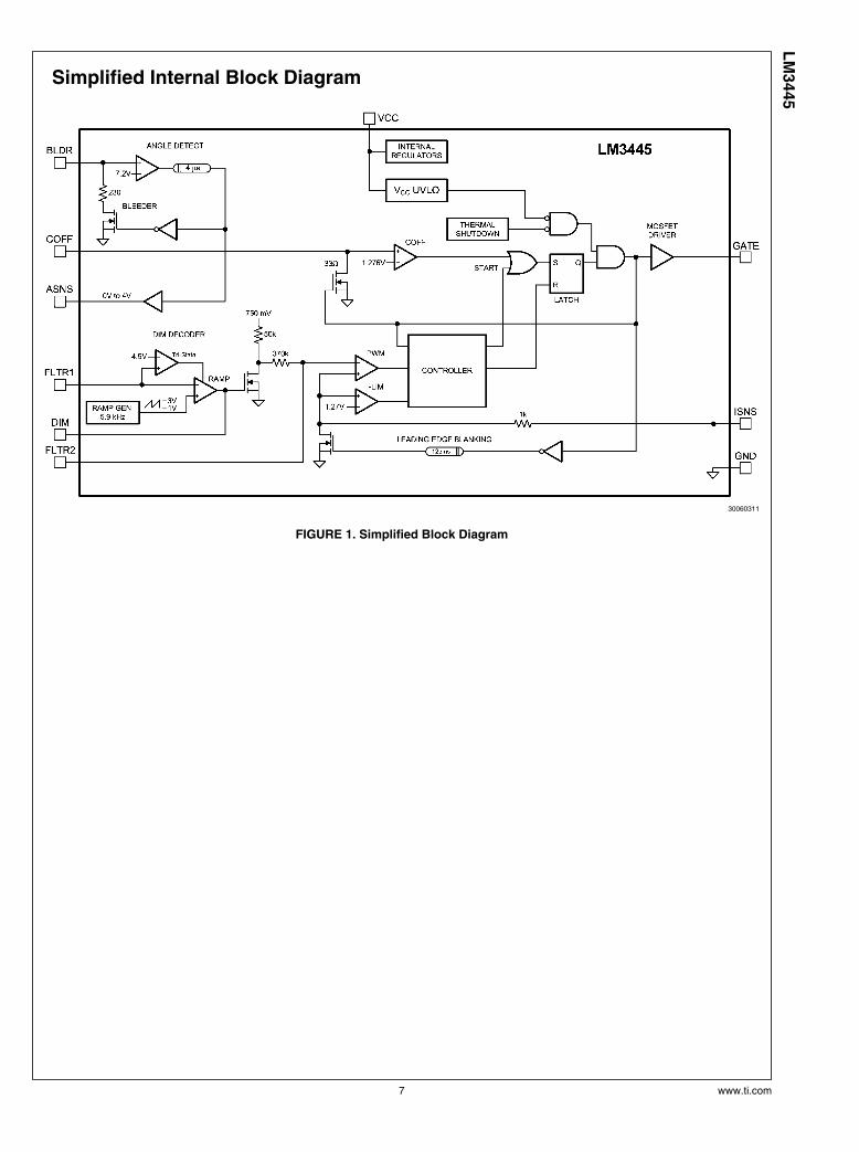
Simplified Internal Block Diagram
30060311
FIGURE 1. Simplified Block Diagram
7 www.ti.com
LM
3445
Application Information
FUNCTIONAL DESCRIPTION
The LM3445 contains all the necessary circuitry to build a line-powered (mains powered) constant current LED driver whoseoutput current can be controlled with a conventional triac dim-mer.
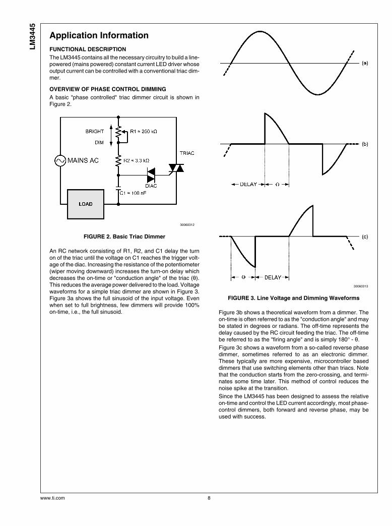
OVERVIEW OF PHASE CONTROL DIMMING
A basic "phase controlled" triac dimmer circuit is shown inFigure 2.
30060312
FIGURE 2. Basic Triac Dimmer
An RC network consisting of R1, R2, and C1 delay the turnon of the triac until the voltage on C1 reaches the trigger volt-age of the diac. Increasing the resistance of the potentiometer(wiper moving downward) increases the turn-on delay whichdecreases the on-time or "conduction angle" of the triac (θ).This reduces the average power delivered to the load. Voltagewaveforms for a simple triac dimmer are shown in Figure 3.Figure 3a shows the full sinusoid of the input voltage. Evenwhen set to full brightness, few dimmers will provide 100%on-time, i.e., the full sinusoid.
30060313
FIGURE 3. Line Voltage and Dimming Waveforms
Figure 3b shows a theoretical waveform from a dimmer. Theon-time is often referred to as the "conduction angle" and maybe stated in degrees or radians. The off-time represents thedelay caused by the RC circuit feeding the triac. The off-timebe referred to as the "firing angle" and is simply 180° - θ.Figure 3c shows a waveform from a so-called reverse phasedimmer, sometimes referred to as an electronic dimmer.These typically are more expensive, microcontroller baseddimmers that use switching elements other than triacs. Notethat the conduction starts from the zero-crossing, and termi-nates some time later. This method of control reduces thenoise spike at the transition.
Since the LM3445 has been designed to assess the relativeon-time and control the LED current accordingly, most phase-control dimmers, both forward and reverse phase, may beused with success.
www.ti.com 8
LM
3445
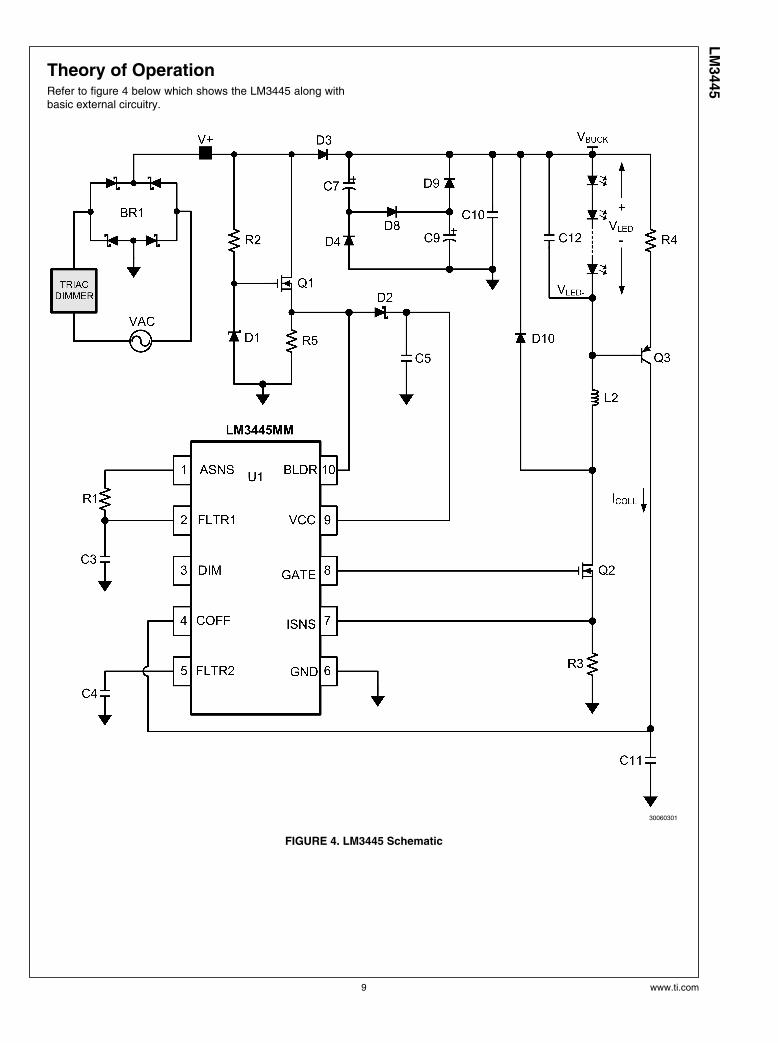
Theory of OperationRefer to figure 4 below which shows the LM3445 along withbasic external circuitry.
30060301
FIGURE 4. LM3445 Schematic
9 www.ti.com
LM
3445
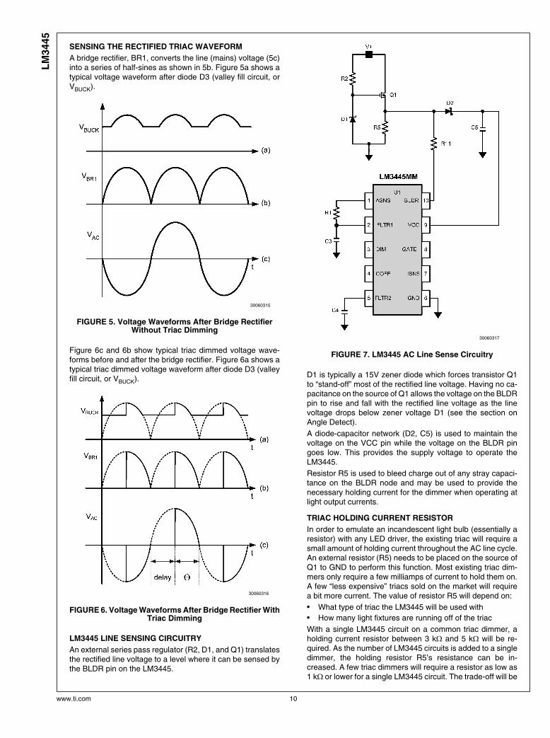
SENSING THE RECTIFIED TRIAC WAVEFORM
A bridge rectifier, BR1, converts the line (mains) voltage (5c)into a series of half-sines as shown in 5b. Figure 5a shows atypical voltage waveform after diode D3 (valley fill circuit, orVBUCK).
30060315
FIGURE 5. Voltage Waveforms After Bridge RectifierWithout Triac Dimming
Figure 6c and 6b show typical triac dimmed voltage wave-forms before and after the bridge rectifier. Figure 6a shows atypical triac dimmed voltage waveform after diode D3 (valleyfill circuit, or VBUCK).
30060316
FIGURE 6. Voltage Waveforms After Bridge Rectifier WithTriac Dimming
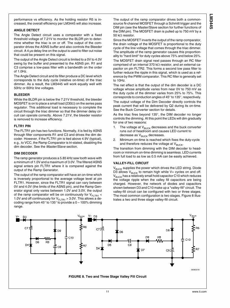
LM3445 LINE SENSING CIRCUITRY
An external series pass regulator (R2, D1, and Q1) translatesthe rectified line voltage to a level where it can be sensed bythe BLDR pin on the LM3445.
30060317
FIGURE 7. LM3445 AC Line Sense Circuitry
D1 is typically a 15V zener diode which forces transistor Q1to “stand-off” most of the rectified line voltage. Having no ca-pacitance on the source of Q1 allows the voltage on the BLDRpin to rise and fall with the rectified line voltage as the linevoltage drops below zener voltage D1 (see the section onAngle Detect).
A diode-capacitor network (D2, C5) is used to maintain thevoltage on the VCC pin while the voltage on the BLDR pingoes low. This provides the supply voltage to operate theLM3445.
Resistor R5 is used to bleed charge out of any stray capaci-tance on the BLDR node and may be used to provide thenecessary holding current for the dimmer when operating atlight output currents.
TRIAC HOLDING CURRENT RESISTOR
In order to emulate an incandescent light bulb (essentially aresistor) with any LED driver, the existing triac will require asmall amount of holding current throughout the AC line cycle.An external resistor (R5) needs to be placed on the source ofQ1 to GND to perform this function. Most existing triac dim-mers only require a few milliamps of current to hold them on.A few “less expensive” triacs sold on the market will requirea bit more current. The value of resistor R5 will depend on:
• What type of triac the LM3445 will be used with
• How many light fixtures are running off of the triac
With a single LM3445 circuit on a common triac dimmer, aholding current resistor between 3 kΩ and 5 kΩ will be re-quired. As the number of LM3445 circuits is added to a singledimmer, the holding resistor R5’s resistance can be in-creased. A few triac dimmers will require a resistor as low as1 kΩ or lower for a single LM3445 circuit. The trade-off will be
www.ti.com 10
LM
3445
performance vs efficiency. As the holding resistor R5 is in-creased, the overall efficiency per LM3445 will also increase.
ANGLE DETECT
The Angle Detect circuit uses a comparator with a fixedthreshold voltage of 7.21V to monitor the BLDR pin to deter-mine whether the triac is on or off. The output of the com-parator drives the ASNS buffer and also controls the Bleedercircuit. A 4 µs delay line on the output is used to filter out noisethat could be present on this signal.
The output of the Angle Detect circuit is limited to a 0V to 4.0Vswing by the buffer and presented to the ASNS pin. R1 andC3 comprise a low-pass filter with a bandwidth on the orderof 1.0Hz.
The Angle Detect circuit and its filter produce a DC level whichcorresponds to the duty cycle (relative on-time) of the triacdimmer. As a result, the LM3445 will work equally well with50Hz or 60Hz line voltages.
BLEEDER
While the BLDR pin is below the 7.21V threshold, the bleederMOSFET is on to place a small load (230Ω) on the series passregulator. This additional load is necessary to complete thecircuit through the triac dimmer so that the dimmer delay cir-cuit can operate correctly. Above 7.21V, the bleeder resistoris removed to increase efficiency.
FLTR1 PIN
The FLTR1 pin has two functions. Normally, it is fed by ASNSthrough filter components R1 and C3 and drives the dim de-coder. However, if the FLTR1 pin is tied above 4.9V (typical),e.g., to VCC, the Ramp Comparator is tri-stated, disabling thedim decoder. See the Master/Slave section.
DIM DECODER
The ramp generator produces a 5.85 kHz saw tooth wave witha minimum of 1.0V and a maximum of 3.0V. The filtered ASNSsignal enters pin FLTR1 where it is compared against theoutput of the Ramp Generator.
The output of the ramp comparator will have an on-time whichis inversely proportional to the average voltage level at pinFLTR1. However, since the FLTR1 signal can vary between0V and 4.0V (the limits of the ASNS pin), and the Ramp Gen-erator signal only varies between 1.0V and 3.0V, the outputof the ramp comparator will be on continuously for VFLTR1 <1.0V and off continuously for VFLTR1 > 3.0V. This allows a de-coding range from 45° to 135° to provide a 0 – 100% dimmingrange.
The output of the ramp comparator drives both a common-source N-channel MOSFET through a Schmitt trigger and theDIM pin (see the Master/Slave section for further functions ofthe DIM pin). The MOSFET drain is pulled up to 750 mV by a50 kΩ resistor.
Since the MOSFET inverts the output of the ramp comparator,the drain voltage of the MOSFET is proportional to the dutycycle of the line voltage that comes through the triac dimmer.The amplitude of the ramp generator causes this proportion-ality to "hard limit" for duty cycles above 75% and below 25%.
The MOSFET drain signal next passes through an RC filtercomprised of an internal 370 kΩ resistor, and an external ca-pacitor on pin FLTR2. This forms a second low pass filter tofurther reduce the ripple in this signal, which is used as a ref-erence by the PWM comparator. This RC filter is generally setto 10Hz.
The net effect is that the output of the dim decoder is a DCvoltage whose amplitude varies from near 0V to 750 mV asthe duty cycle of the dimmer varies from 25% to 75%. Thiscorresponds to conduction angles of 45° to 135°, respectively.
The output voltage of the Dim Decoder directly controls thepeak current that will be delivered by Q2 during its on-time.See the Buck Converter section for details.
As the triac fires beyond 135°, the DIM decoder no longercontrols the dimming. At this point the LEDs will dim graduallyfor one of two reasons:
1. The voltage at VBUCK decreases and the buck converterruns out of headroom and causes LED current todecrease as VBUCK decreases.
2. Minimum on-time is reached which fixes the duty-cycleand therefore reduces the voltage at VBUCK.
The transition from dimming with the DIM decoder to head-room or minimum on-time dimming is seamless. LED currentsfrom full load to as low as 0.5 mA can be easily achieved.
VALLEY-FILL CIRCUIT
VBUCK supplies the power which drives the LED string. DiodeD3 allows VBUCK to remain high while V+ cycles on and off.VBUCK has a relatively small hold capacitor C10 which reducesthe voltage ripple when the valley fill capacitors are beingcharged. However, the network of diodes and capacitorsshown between D3 and C10 make up a "valley-fill" circuit. Thevalley-fill circuit can be configured with two or three stages.The most common configuration is two stages. Figure 8 illus-trates a two and three stage valley-fill circuit.
30060318
FIGURE 8. Two and Three Stage Valley Fill Circuit
11 www.ti.com
LM
3445
The valley-fill circuit allows the buck regulator to draw powerthroughout a larger portion of the AC line. This allows the ca-pacitance needed at VBUCK to be lower than if there were novalley-fill circuit, and adds passive power factor correction(PFC) to the application. Besides better power factor correc-tion, a valley-fill circuit allows the buck converter to operatewhile separate circuitry translates the dimming information.This allows for dimming that isn’t subject to 120Hz flicker thatcan be perceived by the human eye.
VALLEY-FILL OPERATION
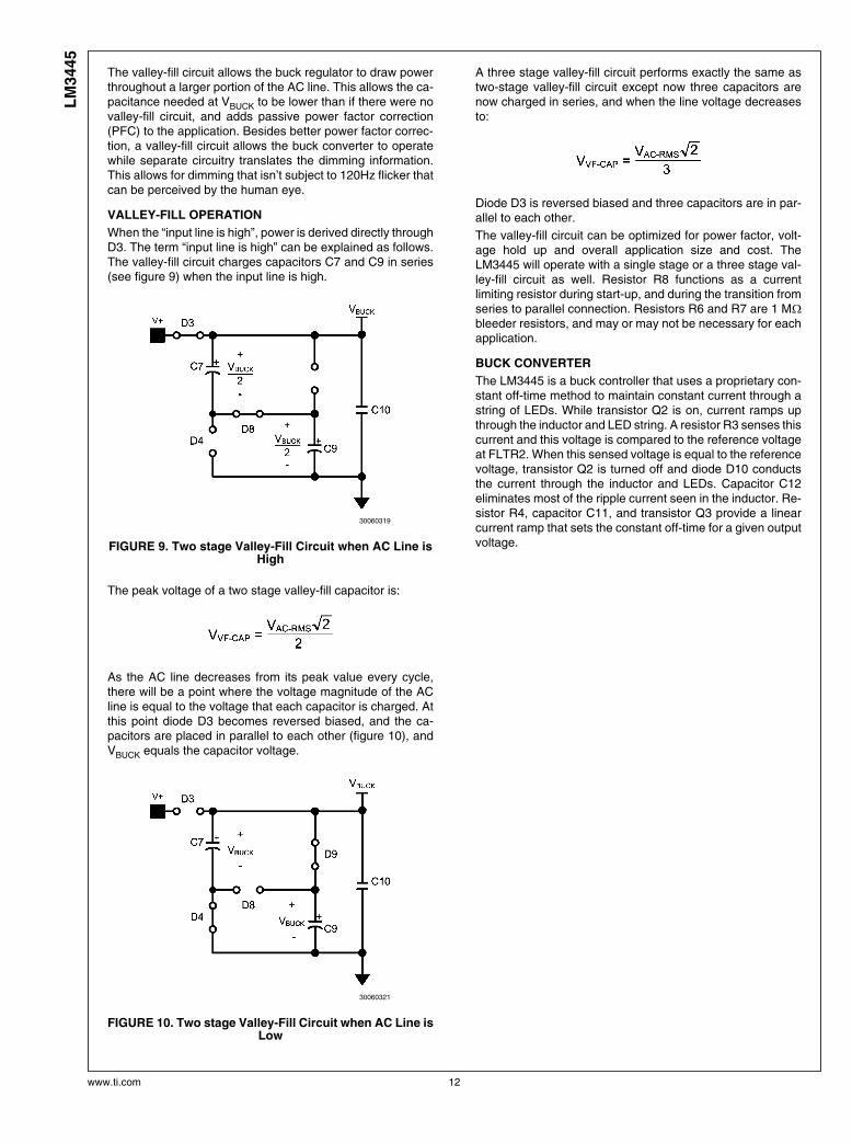
When the “input line is high”, power is derived directly throughD3. The term “input line is high” can be explained as follows.The valley-fill circuit charges capacitors C7 and C9 in series(see figure 9) when the input line is high.
30060319
FIGURE 9. Two stage Valley-Fill Circuit when AC Line isHigh
The peak voltage of a two stage valley-fill capacitor is:
As the AC line decreases from its peak value every cycle,there will be a point where the voltage magnitude of the ACline is equal to the voltage that each capacitor is charged. Atthis point diode D3 becomes reversed biased, and the ca-pacitors are placed in parallel to each other (figure 10), andVBUCK equals the capacitor voltage.
30060321
FIGURE 10. Two stage Valley-Fill Circuit when AC Line isLow
A three stage valley-fill circuit performs exactly the same astwo-stage valley-fill circuit except now three capacitors arenow charged in series, and when the line voltage decreasesto:
Diode D3 is reversed biased and three capacitors are in par-allel to each other.
The valley-fill circuit can be optimized for power factor, volt-age hold up and overall application size and cost. TheLM3445 will operate with a single stage or a three stage val-ley-fill circuit as well. Resistor R8 functions as a currentlimiting resistor during start-up, and during the transition fromseries to parallel connection. Resistors R6 and R7 are 1 MΩbleeder resistors, and may or may not be necessary for eachapplication.
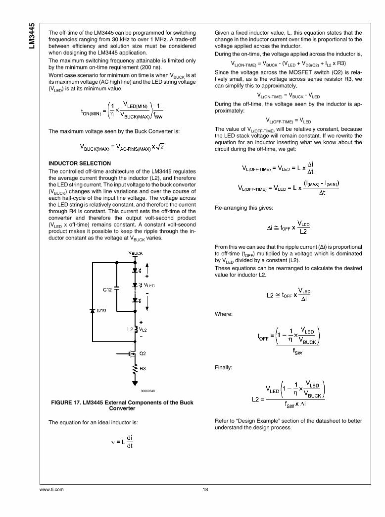
BUCK CONVERTER
The LM3445 is a buck controller that uses a proprietary con-stant off-time method to maintain constant current through astring of LEDs. While transistor Q2 is on, current ramps upthrough the inductor and LED string. A resistor R3 senses thiscurrent and this voltage is compared to the reference voltageat FLTR2. When this sensed voltage is equal to the referencevoltage, transistor Q2 is turned off and diode D10 conductsthe current through the inductor and LEDs. Capacitor C12eliminates most of the ripple current seen in the inductor. Re-sistor R4, capacitor C11, and transistor Q3 provide a linearcurrent ramp that sets the constant off-time for a given outputvoltage.
www.ti.com 12
LM
3445
30060323
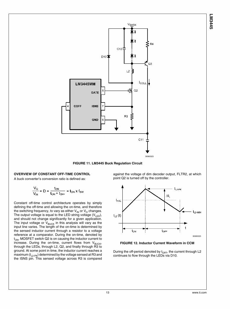
FIGURE 11. LM3445 Buck Regulation Circuit
OVERVIEW OF CONSTANT OFF-TIME CONTROL
A buck converter’s conversion ratio is defined as:
Constant off-time control architecture operates by simplydefining the off-time and allowing the on-time, and thereforethe switching frequency, to vary as either VIN or VO changes.The output voltage is equal to the LED string voltage (VLED),and should not change significantly for a given application.The input voltage or VBUCK in this analysis will vary as theinput line varies. The length of the on-time is determined bythe sensed inductor current through a resistor to a voltagereference at a comparator. During the on-time, denoted bytON, MOSFET switch Q2 is on causing the inductor current toincrease. During the on-time, current flows from VBUCK,through the LEDs, through L2, Q2, and finally through R3 toground. At some point in time, the inductor current reaches amaximum (IL2-PK) determined by the voltage sensed at R3 andthe ISNS pin. This sensed voltage across R3 is compared
against the voltage of dim decoder output, FLTR2, at whichpoint Q2 is turned off by the controller.
30060325
FIGURE 12. Inductor Current Waveform in CCM
During the off-period denoted by tOFF, the current through L2continues to flow through the LEDs via D10.
13 www.ti.com
LM
3445

MASTER/SLAVE OPERATION
Multiple LM3445s can be configured so that large strings ofLEDs can be controlled by a single triac dimmer. By doing so,smooth consistent dimming for multiple LED circuits isachieved.
When the FLTR1 pin is tied above 4.9V (typical), preferablyto VCC, the ramp comparator is tri-stated, disabling the dimdecoder. This allows one or more LM3445 devices or PWMLED driver devices (slaves) to be controlled by a singleLM3445 (master) by connecting their DIM pins together.
MASTER/SLAVE CONFIGURATION
National Semiconductor offers an LM3445 demonstrationPCB for customer evaluation through our website. The fol-lowing description and theory uses reference designators thatfollow our evaluation PCB. The LM3445 Master/Slaveschematics are illustrated below (figures 13 - 15) for clarity.Each board contains a separate circuit for the Master andSlave function. Both the Master and Slave boards will needto be modified from their original stand alone function so thatthey can be coupled together. Only the Master LM3445 re-quires use of the Master/Slave circuit for any number ofslaves.
MASTER BOARD MODIFICATIONS
• Remove R10 and replace with a BAS40 diode
• Connect TP18 to TP14 (VCC)
• Connect TP17 (gate of Q5) to TP15 (gate of Q2)
SLAVE BOARD(S) MODIFICATIONS
• Remove R11 (disconnects BLDR)
• Tie TP14 (FLTR1) to VCC
MASTER/SLAVE(S) INTERCONNECTION
• Connect TP19 of Master to TP10 of Slave (Master VCCControl)
• Connect TP6 (DIM pin) of Master to TP6 (DIM pin) of Slave(Master DIM Control)
MASTER/SLAVE THEORY OF OPERATION
By placing two series diodes on the Master VCC circuit oneforces the master VCC UVLO to become the dominant thresh-old. When Master VCC drops below UVLO, GATE stopsswitching and the RC timer (>200 µs) rises above the TL431threshold (2.5V) which in turn pulls down on the gate of theSlave pass device (Q1).
The valley-fill circuit could consist of one large circuit to powerall LM3445 series connected, or each LM3445 circuit couldhave a separate valley-fill circuit located near the buck con-verter.
www.ti.com 14
LM
3445
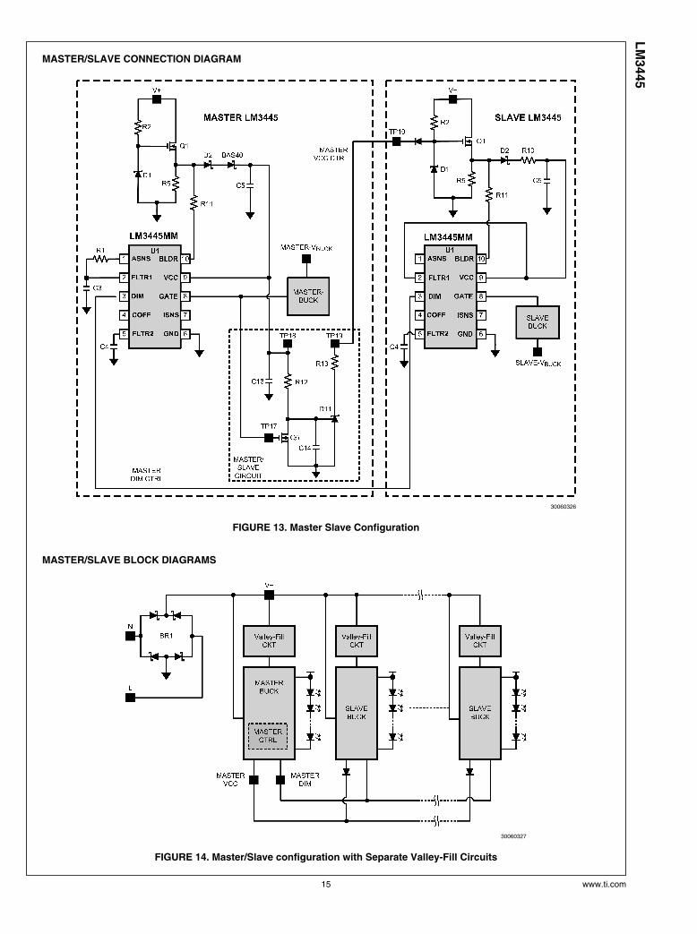
MASTER/SLAVE CONNECTION DIAGRAM
30060326
FIGURE 13. Master Slave Configuration
MASTER/SLAVE BLOCK DIAGRAMS
30060327
FIGURE 14. Master/Slave configuration with Separate Valley-Fill Circuits
15 www.ti.com
LM
3445
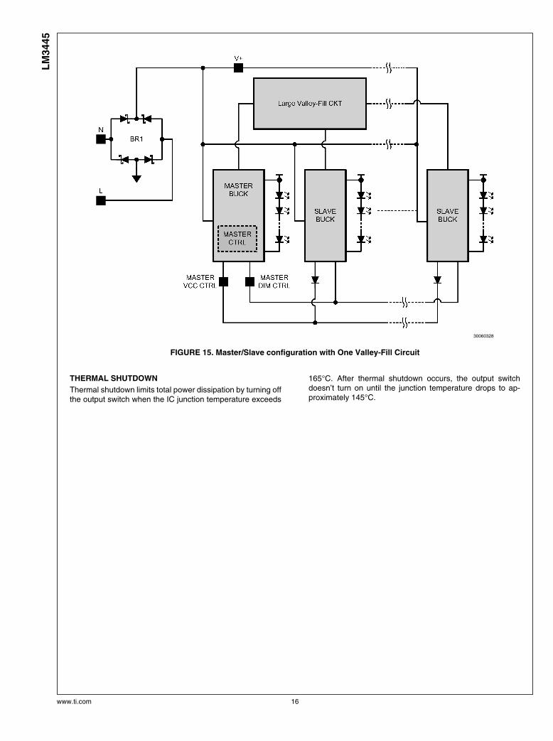
30060328
FIGURE 15. Master/Slave configuration with One Valley-Fill Circuit
THERMAL SHUTDOWN
Thermal shutdown limits total power dissipation by turning offthe output switch when the IC junction temperature exceeds
165°C. After thermal shutdown occurs, the output switchdoesn’t turn on until the junction temperature drops to ap-proximately 145°C.
www.ti.com 16
LM
3445
Design Guide
DETERMINING DUTY-CYCLE (D)
Duty cycle (D) approximately equals:
With efficiency considered:
For simplicity, choose efficiency between 75% and 85%.
CALCULATING OFF-TIME
The “Off-Time” of the LM3445 is set by the user and remainsfairly constant as long as the voltage of the LED stack remainsconstant. Calculating the off-time is the first step in determin-ing the switching frequency of the converter, which is integralin determining some external component values.
PNP transistor Q3, resistor R4, and the LED string voltagedefine a charging current into capacitor C11. A constant cur-rent into a capacitor creates a linear charging characteristic.
Resistor R4, capacitor C11 and the current through resistorR4 (iCOLL), which is approximately equal to VLED/R4, are allfixed. Therefore, dv is fixed and linear, and dt (tOFF) can nowbe calculated.
Common equations for determining duty cycle and switchingfrequency in any buck converter:
Therefore:
With efficiency of the buck converter in mind:
Substitute equations and rearrange:
Off-time, and switching frequency can now be calculated us-ing the equations above.
SETTING THE SWITCHING FREQUENCY
Selecting the switching frequency for nominal operating con-ditions is based on tradeoffs between efficiency (better at lowfrequency) and solution size/cost (smaller at high frequency).
The input voltage to the buck converter (VBUCK) changes withboth line variations and over the course of each half-cycle ofthe input line voltage. The voltage across the LED string will,however, remain constant, and therefore the off-time remainsconstant.
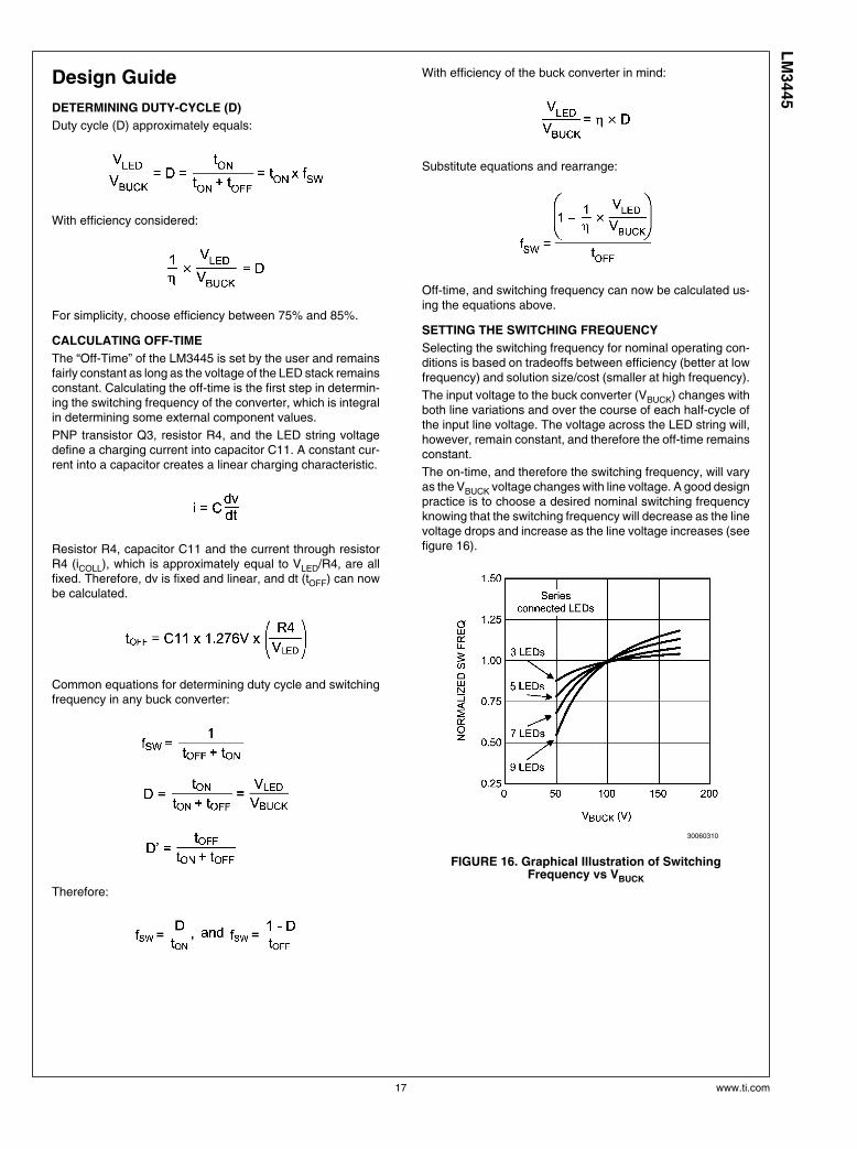
The on-time, and therefore the switching frequency, will varyas the VBUCK voltage changes with line voltage. A good designpractice is to choose a desired nominal switching frequencyknowing that the switching frequency will decrease as the linevoltage drops and increase as the line voltage increases (seefigure 16).
30060310
FIGURE 16. Graphical Illustration of SwitchingFrequency vs VBUCK
17 www.ti.com
LM
3445
The off-time of the LM3445 can be programmed for switchingfrequencies ranging from 30 kHz to over 1 MHz. A trade-offbetween efficiency and solution size must be consideredwhen designing the LM3445 application.
The maximum switching frequency attainable is limited onlyby the minimum on-time requirement (200 ns).
Worst case scenario for minimum on time is when VBUCK is atits maximum voltage (AC high line) and the LED string voltage(VLED) is at its minimum value.
The maximum voltage seen by the Buck Converter is:
INDUCTOR SELECTION
The controlled off-time architecture of the LM3445 regulatesthe average current through the inductor (L2), and thereforethe LED string current. The input voltage to the buck converter(VBUCK) changes with line variations and over the course ofeach half-cycle of the input line voltage. The voltage acrossthe LED string is relatively constant, and therefore the currentthrough R4 is constant. This current sets the off-time of theconverter and therefore the output volt-second product(VLED x off-time) remains constant. A constant volt-secondproduct makes it possible to keep the ripple through the in-ductor constant as the voltage at VBUCK varies.
30060340
FIGURE 17. LM3445 External Components of the BuckConverter
The equation for an ideal inductor is:
Given a fixed inductor value, L, this equation states that thechange in the inductor current over time is proportional to thevoltage applied across the inductor.
During the on-time, the voltage applied across the inductor is,
VL(ON-TIME) = VBUCK - (VLED + VDS(Q2) + IL2 x R3)
Since the voltage across the MOSFET switch (Q2) is rela-tively small, as is the voltage across sense resistor R3, wecan simplify this to approximately,
VL(ON-TIME) = VBUCK - VLED
During the off-time, the voltage seen by the inductor is ap-proximately:
VL(OFF-TIME) = VLED
The value of VL(OFF-TIME) will be relatively constant, becausethe LED stack voltage will remain constant. If we rewrite theequation for an inductor inserting what we know about thecircuit during the off-time, we get:
Re-arranging this gives:
From this we can see that the ripple current (Δi) is proportionalto off-time (tOFF) multiplied by a voltage which is dominatedby VLED divided by a constant (L2).
These equations can be rearranged to calculate the desiredvalue for inductor L2.
Where:
Finally:
Refer to “Design Example” section of the datasheet to betterunderstand the design process.
www.ti.com 18
LM
3445
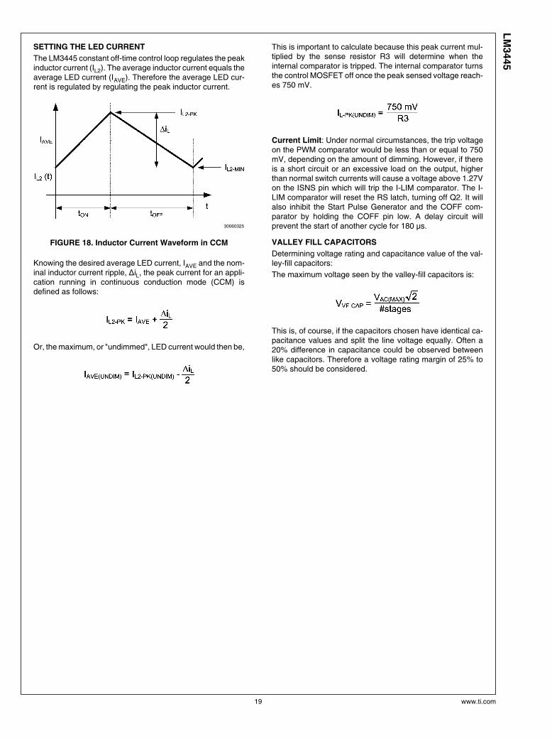
SETTING THE LED CURRENT
The LM3445 constant off-time control loop regulates the peakinductor current (IL2). The average inductor current equals theaverage LED current (IAVE). Therefore the average LED cur-rent is regulated by regulating the peak inductor current.
30060325
FIGURE 18. Inductor Current Waveform in CCM
Knowing the desired average LED current, IAVE and the nom-inal inductor current ripple, ΔiL, the peak current for an appli-cation running in continuous conduction mode (CCM) isdefined as follows:
Or, the maximum, or "undimmed", LED current would then be,
This is important to calculate because this peak current mul-tiplied by the sense resistor R3 will determine when theinternal comparator is tripped. The internal comparator turnsthe control MOSFET off once the peak sensed voltage reach-es 750 mV.
Current Limit: Under normal circumstances, the trip voltageon the PWM comparator would be less than or equal to 750mV, depending on the amount of dimming. However, if thereis a short circuit or an excessive load on the output, higherthan normal switch currents will cause a voltage above 1.27Von the ISNS pin which will trip the I-LIM comparator. The I-LIM comparator will reset the RS latch, turning off Q2. It willalso inhibit the Start Pulse Generator and the COFF com-parator by holding the COFF pin low. A delay circuit willprevent the start of another cycle for 180 µs.
VALLEY FILL CAPACITORS
Determining voltage rating and capacitance value of the val-ley-fill capacitors:
The maximum voltage seen by the valley-fill capacitors is:
This is, of course, if the capacitors chosen have identical ca-pacitance values and split the line voltage equally. Often a20% difference in capacitance could be observed betweenlike capacitors. Therefore a voltage rating margin of 25% to50% should be considered.
19 www.ti.com
LM
3445
Determining the capacitance value of the valley-fill ca-pacitors:
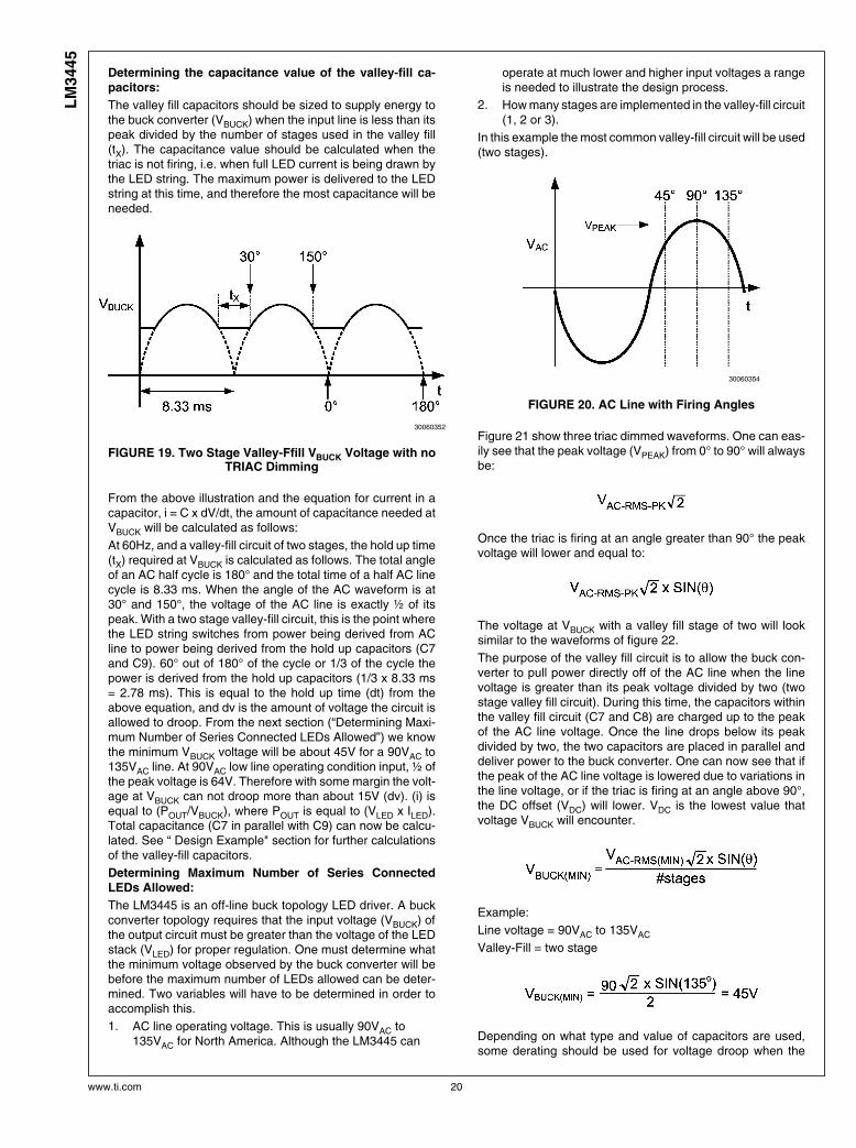
The valley fill capacitors should be sized to supply energy tothe buck converter (VBUCK) when the input line is less than itspeak divided by the number of stages used in the valley fill(tX). The capacitance value should be calculated when thetriac is not firing, i.e. when full LED current is being drawn bythe LED string. The maximum power is delivered to the LEDstring at this time, and therefore the most capacitance will beneeded.
30060352
FIGURE 19. Two Stage Valley-Ffill VBUCK Voltage with noTRIAC Dimming
From the above illustration and the equation for current in acapacitor, i = C x dV/dt, the amount of capacitance needed atVBUCK will be calculated as follows:
At 60Hz, and a valley-fill circuit of two stages, the hold up time(tX) required at VBUCK is calculated as follows. The total angleof an AC half cycle is 180° and the total time of a half AC linecycle is 8.33 ms. When the angle of the AC waveform is at30° and 150°, the voltage of the AC line is exactly ½ of itspeak. With a two stage valley-fill circuit, this is the point wherethe LED string switches from power being derived from ACline to power being derived from the hold up capacitors (C7and C9). 60° out of 180° of the cycle or 1/3 of the cycle thepower is derived from the hold up capacitors (1/3 x 8.33 ms= 2.78 ms). This is equal to the hold up time (dt) from theabove equation, and dv is the amount of voltage the circuit isallowed to droop. From the next section (“Determining Maxi-mum Number of Series Connected LEDs Allowed”) we knowthe minimum VBUCK voltage will be about 45V for a 90VAC to135VAC line. At 90VAC low line operating condition input, ½ ofthe peak voltage is 64V. Therefore with some margin the volt-age at VBUCK can not droop more than about 15V (dv). (i) isequal to (POUT/VBUCK), where POUT is equal to (VLED x ILED).Total capacitance (C7 in parallel with C9) can now be calcu-lated. See “ Design Example" section for further calculationsof the valley-fill capacitors.
Determining Maximum Number of Series ConnectedLEDs Allowed:
The LM3445 is an off-line buck topology LED driver. A buckconverter topology requires that the input voltage (VBUCK) ofthe output circuit must be greater than the voltage of the LEDstack (VLED) for proper regulation. One must determine whatthe minimum voltage observed by the buck converter will bebefore the maximum number of LEDs allowed can be deter-mined. Two variables will have to be determined in order toaccomplish this.
1. AC line operating voltage. This is usually 90VAC to135VAC for North America. Although the LM3445 can
operate at much lower and higher input voltages a rangeis needed to illustrate the design process.
2. How many stages are implemented in the valley-fill circuit(1, 2 or 3).
In this example the most common valley-fill circuit will be used(two stages).
30060354
FIGURE 20. AC Line with Firing Angles
Figure 21 show three triac dimmed waveforms. One can eas-ily see that the peak voltage (VPEAK) from 0° to 90° will alwaysbe:
Once the triac is firing at an angle greater than 90° the peakvoltage will lower and equal to:
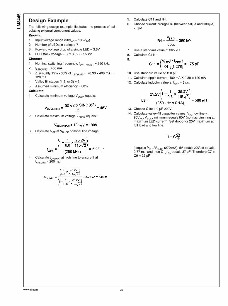
The voltage at VBUCK with a valley fill stage of two will looksimilar to the waveforms of figure 22.
The purpose of the valley fill circuit is to allow the buck con-verter to pull power directly off of the AC line when the linevoltage is greater than its peak voltage divided by two (twostage valley fill circuit). During this time, the capacitors withinthe valley fill circuit (C7 and C8) are charged up to the peakof the AC line voltage. Once the line drops below its peakdivided by two, the two capacitors are placed in parallel anddeliver power to the buck converter. One can now see that ifthe peak of the AC line voltage is lowered due to variations inthe line voltage, or if the triac is firing at an angle above 90°,the DC offset (VDC) will lower. VDC is the lowest value thatvoltage VBUCK will encounter.
Example:
Line voltage = 90VAC to 135VAC
Valley-Fill = two stage
Depending on what type and value of capacitors are used,some derating should be used for voltage droop when the
www.ti.com 20
LM
3445
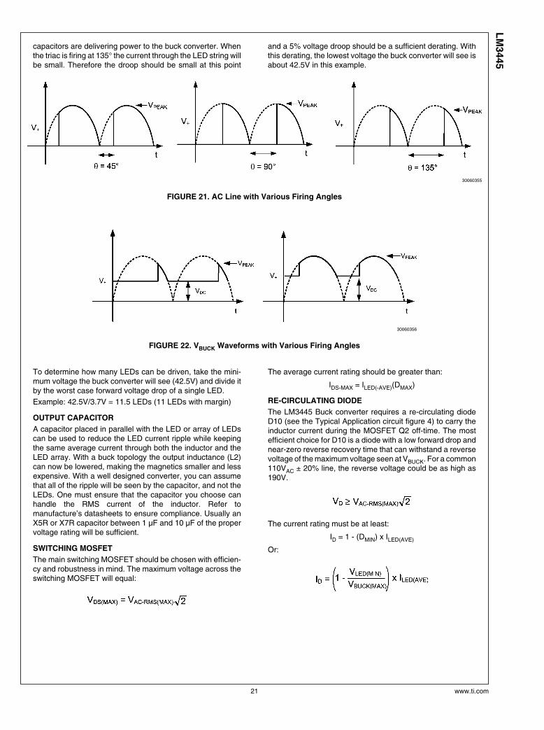
capacitors are delivering power to the buck converter. Whenthe triac is firing at 135° the current through the LED string willbe small. Therefore the droop should be small at this point
and a 5% voltage droop should be a sufficient derating. Withthis derating, the lowest voltage the buck converter will see isabout 42.5V in this example.
30060355
FIGURE 21. AC Line with Various Firing Angles
30060356
FIGURE 22. VBUCK Waveforms with Various Firing Angles
To determine how many LEDs can be driven, take the mini-mum voltage the buck converter will see (42.5V) and divide itby the worst case forward voltage drop of a single LED.
Example: 42.5V/3.7V = 11.5 LEDs (11 LEDs with margin)
OUTPUT CAPACITOR
A capacitor placed in parallel with the LED or array of LEDscan be used to reduce the LED current ripple while keepingthe same average current through both the inductor and theLED array. With a buck topology the output inductance (L2)can now be lowered, making the magnetics smaller and lessexpensive. With a well designed converter, you can assumethat all of the ripple will be seen by the capacitor, and not theLEDs. One must ensure that the capacitor you choose canhandle the RMS current of the inductor. Refer tomanufacture’s datasheets to ensure compliance. Usually anX5R or X7R capacitor between 1 µF and 10 µF of the propervoltage rating will be sufficient.
SWITCHING MOSFET
The main switching MOSFET should be chosen with efficien-cy and robustness in mind. The maximum voltage across theswitching MOSFET will equal:
The average current rating should be greater than:
IDS-MAX = ILED(-AVE)(DMAX)
RE-CIRCULATING DIODE
The LM3445 Buck converter requires a re-circulating diodeD10 (see the Typical Application circuit figure 4) to carry theinductor current during the MOSFET Q2 off-time. The mostefficient choice for D10 is a diode with a low forward drop andnear-zero reverse recovery time that can withstand a reversevoltage of the maximum voltage seen at VBUCK. For a common110VAC ± 20% line, the reverse voltage could be as high as190V.
The current rating must be at least:
ID = 1 - (DMIN) x ILED(AVE)
Or:
21 www.ti.com
LM
3445
Design ExampleThe following design example illustrates the process of cal-culating external component values.
Known:
1. Input voltage range (90VAC – 135VAC)
2. Number of LEDs in series = 7
3. Forward voltage drop of a single LED = 3.6V
4. LED stack voltage = (7 x 3.6V) = 25.2V
Choose:
1. Nominal switching frequency, fSW-TARGET = 250 kHz
2. ILED(AVE) = 400 mA
3. Δi (usually 15% - 30% of ILED(AVE)) = (0.30 x 400 mA) =120 mA
4. Valley fill stages (1,2, or 3) = 2
5. Assumed minimum efficiency = 80%
Calculate:
1. Calculate minimum voltage VBUCK equals:
2. Calculate maximum voltage VBUCK equals:
3. Calculate tOFF at VBUCK nominal line voltage:
4. Calculate tON(MIN) at high line to ensure thattON(MIN) > 200 ns:
5. Calculate C11 and R4:
6. Choose current through R4: (between 50 µA and 100 µA)70 µA
7. Use a standard value of 365 kΩ8. Calculate C11:
9.
10. Use standard value of 120 pF
11. Calculate ripple current: 400 mA X 0.30 = 120 mA
12. Calculate inductor value at tOFF = 3 µs:
13. Choose C10: 1.0 µF 200V
14. Calculate valley-fill capacitor values: VAC low line =90VAC, VBUCK minimum equals 60V (no triac dimming atmaximum LED current). Set droop for 20V maximum atfull load and low line.
i) equals POUT/VBUCK (270 mA), dV equals 20V, dt equals2.77 ms, and then CTOTAL equals 37 µF. Therefore C7 =C9 = 22 µF
www.ti.com 22
LM
3445
LM3445 Design Example 1
Input = 90VAC to 135VAC, VLED = 7 x HB LED String Application @ 400 mA
30060369
23 www.ti.com
LM
3445
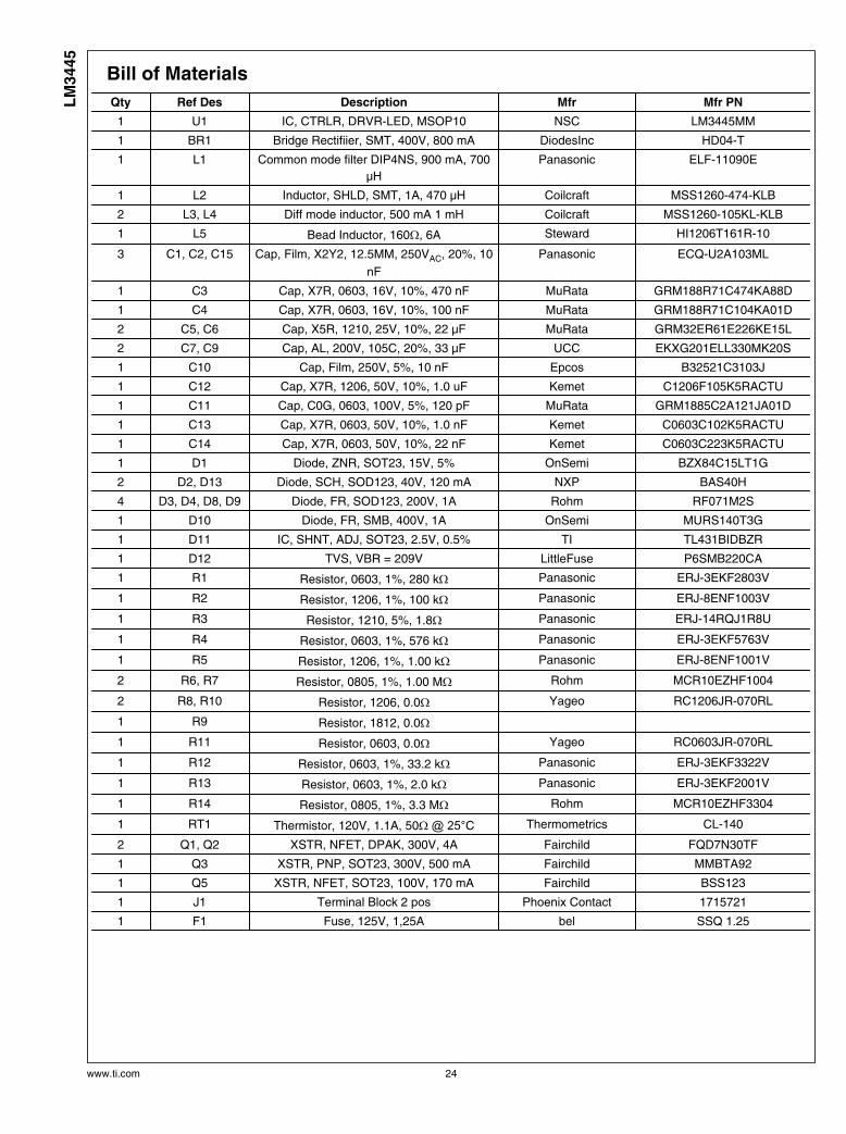
Bill of Materials
Qty Ref Des Description Mfr Mfr PN
1 U1 IC, CTRLR, DRVR-LED, MSOP10 NSC LM3445MM
1 BR1 Bridge Rectifiier, SMT, 400V, 800 mA DiodesInc HD04-T
1 L1 Common mode filter DIP4NS, 900 mA, 700
µH
Panasonic ELF-11090E
1 L2 Inductor, SHLD, SMT, 1A, 470 µH Coilcraft MSS1260-474-KLB
2 L3, L4 Diff mode inductor, 500 mA 1 mH Coilcraft MSS1260-105KL-KLB
1 L5 Bead Inductor, 160Ω, 6A Steward HI1206T161R-10
3 C1, C2, C15 Cap, Film, X2Y2, 12.5MM, 250VAC, 20%, 10
nF
Panasonic ECQ-U2A103ML
1 C3 Cap, X7R, 0603, 16V, 10%, 470 nF MuRata GRM188R71C474KA88D
1 C4 Cap, X7R, 0603, 16V, 10%, 100 nF MuRata GRM188R71C104KA01D
2 C5, C6 Cap, X5R, 1210, 25V, 10%, 22 µF MuRata GRM32ER61E226KE15L
2 C7, C9 Cap, AL, 200V, 105C, 20%, 33 µF UCC EKXG201ELL330MK20S
1 C10 Cap, Film, 250V, 5%, 10 nF Epcos B32521C3103J
1 C12 Cap, X7R, 1206, 50V, 10%, 1.0 uF Kemet C1206F105K5RACTU
1 C11 Cap, C0G, 0603, 100V, 5%, 120 pF MuRata GRM1885C2A121JA01D
1 C13 Cap, X7R, 0603, 50V, 10%, 1.0 nF Kemet C0603C102K5RACTU
1 C14 Cap, X7R, 0603, 50V, 10%, 22 nF Kemet C0603C223K5RACTU
1 D1 Diode, ZNR, SOT23, 15V, 5% OnSemi BZX84C15LT1G
2 D2, D13 Diode, SCH, SOD123, 40V, 120 mA NXP BAS40H
4 D3, D4, D8, D9 Diode, FR, SOD123, 200V, 1A Rohm RF071M2S
1 D10 Diode, FR, SMB, 400V, 1A OnSemi MURS140T3G
1 D11 IC, SHNT, ADJ, SOT23, 2.5V, 0.5% TI TL431BIDBZR
1 D12 TVS, VBR = 209V LittleFuse P6SMB220CA
1 R1 Resistor, 0603, 1%, 280 kΩ Panasonic ERJ-3EKF2803V
1 R2 Resistor, 1206, 1%, 100 kΩ Panasonic ERJ-8ENF1003V
1 R3 Resistor, 1210, 5%, 1.8Ω Panasonic ERJ-14RQJ1R8U
1 R4 Resistor, 0603, 1%, 576 kΩ Panasonic ERJ-3EKF5763V
1 R5 Resistor, 1206, 1%, 1.00 kΩ Panasonic ERJ-8ENF1001V
2 R6, R7 Resistor, 0805, 1%, 1.00 MΩ Rohm MCR10EZHF1004
2 R8, R10 Resistor, 1206, 0.0Ω Yageo RC1206JR-070RL
1 R9 Resistor, 1812, 0.0Ω
1 R11 Resistor, 0603, 0.0Ω Yageo RC0603JR-070RL
1 R12 Resistor, 0603, 1%, 33.2 kΩ Panasonic ERJ-3EKF3322V
1 R13 Resistor, 0603, 1%, 2.0 kΩ Panasonic ERJ-3EKF2001V
1 R14 Resistor, 0805, 1%, 3.3 MΩ Rohm MCR10EZHF3304
1 RT1 Thermistor, 120V, 1.1A, 50Ω @ 25°C Thermometrics CL-140
2 Q1, Q2 XSTR, NFET, DPAK, 300V, 4A Fairchild FQD7N30TF
1 Q3 XSTR, PNP, SOT23, 300V, 500 mA Fairchild MMBTA92
1 Q5 XSTR, NFET, SOT23, 100V, 170 mA Fairchild BSS123
1 J1 Terminal Block 2 pos Phoenix Contact 1715721
1 F1 Fuse, 125V, 1,25A bel SSQ 1.25
www.ti.com 24
LM
3445
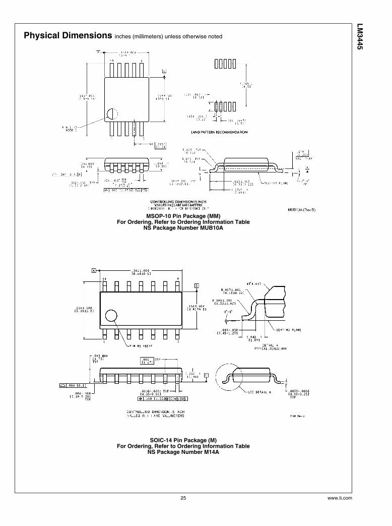
Physical Dimensions inches (millimeters) unless otherwise noted
MSOP-10 Pin Package (MM)For Ordering, Refer to Ordering Information Table
NS Package Number MUB10A
SOIC-14 Pin Package (M)For Ordering, Refer to Ordering Information Table
NS Package Number M14A
25 www.ti.com
LM
3445
NotesL
M3445 T
riac D
imm
ab
le O
fflin
e L
ED
Dri
ver
TI/NATIONAL INTERIM IMPORTANT NOTICE
Texas Instruments has purchased National Semiconductor. As of Monday, September 26th, and until further notice, products sold oradvertised under the National Semiconductor name or logo, and information, support and interactions concerning such products, remainsubject to the preexisting National Semiconductor standard terms and conditions of sale, terms of use of website, and Notices (and/orterms previously agreed in writing with National Semiconductor, where applicable) and are not subject to any differing terms and noticesapplicable to other TI components, sales or websites. To the extent information on official TI and National websites and business socialnetworking media, etc., pertains to both TI and National-branded products, both companies' instructions, warnings and limitations in theabove-referenced terms of use apply.
Following are URLs where you can obtain information on other Texas Instruments products and application solutions:
Products Applications
Audio www.ti.com/audio Communications and Telecom www.ti.com/communications
Amplifiers amplifier.ti.com Computers and Peripherals www.ti.com/computers
Data Converters dataconverter.ti.com Consumer Electronics www.ti.com/consumer-apps
DLP® Products www.dlp.com Energy and Lighting www.ti.com/energy
DSP dsp.ti.com Industrial www.ti.com/industrial
Clocks and Timers www.ti.com/clocks Medical www.ti.com/medical
Interface interface.ti.com Security www.ti.com/security
Logic logic.ti.com Space, Avionics and Defense www.ti.com/space-avionics-defense
Power Mgmt power.ti.com Transportation and Automotive www.ti.com/automotive
Microcontrollers microcontroller.ti.com Video and Imaging www.ti.com/video
RFID www.ti-rfid.com Wireless www.ti.com/wireless-apps
RF/IF and ZigBee® Solutions www.ti.com/lprf TI E2E Community Home Page e2e.ti.com
Mailing Address: Texas Instruments, Post Office Box 655303, Dallas, Texas 75265
Copyright© 2011 Texas Instruments Incorporated
www.ti.com

IMPORTANT NOTICE
Texas Instruments Incorporated and its subsidiaries (TI) reserve the right to make corrections, modifications, enhancements, improvements,and other changes to its products and services at any time and to discontinue any product or service without notice. Customers shouldobtain the latest relevant information before placing orders and should verify that such information is current and complete. All products aresold subject to TI’s terms and conditions of sale supplied at the time of order acknowledgment.
TI warrants performance of its hardware products to the specifications applicable at the time of sale in accordance with TI’s standardwarranty. Testing and other quality control techniques are used to the extent TI deems necessary to support this warranty. Except wheremandated by government requirements, testing of all parameters of each product is not necessarily performed.
TI assumes no liability for applications assistance or customer product design. Customers are responsible for their products andapplications using TI components. To minimize the risks associated with customer products and applications, customers should provideadequate design and operating safeguards.
TI does not warrant or represent that any license, either express or implied, is granted under any TI patent right, copyright, mask work right,or other TI intellectual property right relating to any combination, machine, or process in which TI products or services are used. Informationpublished by TI regarding third-party products or services does not constitute a license from TI to use such products or services or awarranty or endorsement thereof. Use of such information may require a license from a third party under the patents or other intellectualproperty of the third party, or a license from TI under the patents or other intellectual property of TI.
Reproduction of TI information in TI data books or data sheets is permissible only if reproduction is without alteration and is accompaniedby all associated warranties, conditions, limitations, and notices. Reproduction of this information with alteration is an unfair and deceptivebusiness practice. TI is not responsible or liable for such altered documentation. Information of third parties may be subject to additionalrestrictions.
Resale of TI products or services with statements different from or beyond the parameters stated by TI for that product or service voids allexpress and any implied warranties for the associated TI product or service and is an unfair and deceptive business practice. TI is notresponsible or liable for any such statements.
TI products are not authorized for use in safety-critical applications (such as life support) where a failure of the TI product would reasonablybe expected to cause severe personal injury or death, unless officers of the parties have executed an agreement specifically governingsuch use. Buyers represent that they have all necessary expertise in the safety and regulatory ramifications of their applications, andacknowledge and agree that they are solely responsible for all legal, regulatory and safety-related requirements concerning their productsand any use of TI products in such safety-critical applications, notwithstanding any applications-related information or support that may beprovided by TI. Further, Buyers must fully indemnify TI and its representatives against any damages arising out of the use of TI products insuch safety-critical applications.
TI products are neither designed nor intended for use in military/aerospace applications or environments unless the TI products arespecifically designated by TI as military-grade or "enhanced plastic." Only products designated by TI as military-grade meet militaryspecifications. Buyers acknowledge and agree that any such use of TI products which TI has not designated as military-grade is solely atthe Buyer's risk, and that they are solely responsible for compliance with all legal and regulatory requirements in connection with such use.
TI products are neither designed nor intended for use in automotive applications or environments unless the specific TI products aredesignated by TI as compliant with ISO/TS 16949 requirements. Buyers acknowledge and agree that, if they use any non-designatedproducts in automotive applications, TI will not be responsible for any failure to meet such requirements.
Following are URLs where you can obtain information on other Texas Instruments products and application solutions:
Products Applications
Audio www.ti.com/audio Communications and Telecom www.ti.com/communications
Amplifiers amplifier.ti.com Computers and Peripherals www.ti.com/computers
Data Converters dataconverter.ti.com Consumer Electronics www.ti.com/consumer-apps
DLP® Products www.dlp.com Energy and Lighting www.ti.com/energy
DSP dsp.ti.com Industrial www.ti.com/industrial
Clocks and Timers www.ti.com/clocks Medical www.ti.com/medical
Interface interface.ti.com Security www.ti.com/security
Logic logic.ti.com Space, Avionics and Defense www.ti.com/space-avionics-defense
Power Mgmt power.ti.com Transportation and Automotive www.ti.com/automotive
Microcontrollers microcontroller.ti.com Video and Imaging www.ti.com/video
RFID www.ti-rfid.com
OMAP Mobile Processors www.ti.com/omap
Wireless Connectivity www.ti.com/wirelessconnectivity
TI E2E Community Home Page e2e.ti.com
Mailing Address: Texas Instruments, Post Office Box 655303, Dallas, Texas 75265Copyright © 2011, Texas Instruments Incorporated