LM2671 Datasheet - TI.com · Product Folder Sample & Buy Technical Documents Tools & Software...
36
Product Folder Sample & Buy Technical Documents Tools & Software Support & Community An IMPORTANT NOTICE at the end of this data sheet addresses availability, warranty, changes, use in safety-critical applications, intellectual property matters and other important disclaimers. PRODUCTION DATA. LM2671 SNVS008L – SEPTEMBER 1998 – REVISED JUNE 2016 LM2671 SIMPLE SWITCHER ® Power Converter High Efficiency 500-mA Step-Down Voltage Regulator With Features 1 1 Features 1• Efficiency up to 96% • Available in 8-Pin SOIC, PDIP, and WSON Packages • Simple and Easy to Design With • Requires Only 5 External Components • Uses Readily Available Standard Inductors • 3.3-V, 5-V, 12-V, and Adjustable Output Versions • Adjustable Version Output Voltage Range: 1.21 V to 37 V • ±1.5% Maximum Output Voltage Tolerance Over Line and Load Conditions • Ensured 500-mA Output Load Current • 0.25-Ω DMOS Output Switch • Wide Input Voltage Range: 8 V to 40 V • 260-kHz Fixed Frequency Internal Oscillator • TTL Shutdown Capability, Low Power Standby Mode • Soft-Start and Frequency Synchronization • Thermal Shutdown and Current-Limit Protection 2 Applications • Simple High Efficiency (> 90%) Step-Down (Buck) Regulators • Efficient Preregulator for Linear Regulators 3 Description The LM2671 series of regulators are monolithic integrated circuits built with a LMDMOS process. These regulators provide all the active functions for a step-down (buck) switching regulator, capable of driving a 500-mA load current with excellent line and load regulation. These devices are available in fixed output voltages of 3.3 V, 5 V, 12 V, and an adjustable output version. Requiring a minimum number of external components, these regulators are simple to use and include patented internal frequency compensation, fixed frequency oscillator, external shutdown, soft start, and frequency synchronization. The LM2671 series operates at a switching frequency of 260 kHz, thus allowing smaller sized filter components than what is required with lower frequency switching regulators. Because of its very high efficiency (> 90%), the copper traces on the printed-circuit board are the only heat sinking required. A family of standard inductors for use with the LM2671 are available from several different manufacturers. This feature greatly simplifies the design of switch-mode power supplies using these advanced ICs. Also included in the data sheet are selector guides for diodes and capacitors designed to work in switch-mode power supplies. Device Information (1) PART NUMBER PACKAGE BODY SIZE (NOM) LM2674 SOIC (8) 4.90 mm × 3.91 mm PDIP (8) 9.81 mm × 6.35 mm WSON (16) 5.00 mm × 5.00 mm (1) For all available packages, see the orderable addendum at the end of the data sheet. Typical Application For fixed output voltage versions
Transcript of LM2671 Datasheet - TI.com · Product Folder Sample & Buy Technical Documents Tools & Software...

Product
Folder
Sample &Buy
Technical
Documents
Tools &
Software
Support &Community
An IMPORTANT NOTICE at the end of this data sheet addresses availability, warranty, changes, use in safety-critical applications,intellectual property matters and other important disclaimers. PRODUCTION DATA.
LM2671SNVS008L –SEPTEMBER 1998–REVISED JUNE 2016
LM2671 SIMPLE SWITCHER® Power Converter High Efficiency 500-mAStep-Down Voltage Regulator With Features
1
1 Features1• Efficiency up to 96%• Available in 8-Pin SOIC, PDIP, and WSON
Packages• Simple and Easy to Design With• Requires Only 5 External Components• Uses Readily Available Standard Inductors• 3.3-V, 5-V, 12-V, and Adjustable Output Versions• Adjustable Version Output Voltage Range: 1.21 V
to 37 V• ±1.5% Maximum Output Voltage Tolerance Over
Line and Load Conditions• Ensured 500-mA Output Load Current• 0.25-Ω DMOS Output Switch• Wide Input Voltage Range: 8 V to 40 V• 260-kHz Fixed Frequency Internal Oscillator• TTL Shutdown Capability, Low Power Standby
Mode• Soft-Start and Frequency Synchronization• Thermal Shutdown and Current-Limit Protection
2 Applications• Simple High Efficiency (> 90%) Step-Down (Buck)
Regulators• Efficient Preregulator for Linear Regulators
3 DescriptionThe LM2671 series of regulators are monolithicintegrated circuits built with a LMDMOS process.These regulators provide all the active functions for astep-down (buck) switching regulator, capable ofdriving a 500-mA load current with excellent line andload regulation. These devices are available in fixedoutput voltages of 3.3 V, 5 V, 12 V, and an adjustableoutput version.
Requiring a minimum number of externalcomponents, these regulators are simple to use andinclude patented internal frequency compensation,fixed frequency oscillator, external shutdown, softstart, and frequency synchronization.
The LM2671 series operates at a switching frequencyof 260 kHz, thus allowing smaller sized filtercomponents than what is required with lowerfrequency switching regulators. Because of its veryhigh efficiency (> 90%), the copper traces on theprinted-circuit board are the only heat sinkingrequired.
A family of standard inductors for use with theLM2671 are available from several differentmanufacturers. This feature greatly simplifies thedesign of switch-mode power supplies using theseadvanced ICs. Also included in the data sheet areselector guides for diodes and capacitors designed towork in switch-mode power supplies.
Device Information(1)
PART NUMBER PACKAGE BODY SIZE (NOM)
LM2674SOIC (8) 4.90 mm × 3.91 mmPDIP (8) 9.81 mm × 6.35 mmWSON (16) 5.00 mm × 5.00 mm
(1) For all available packages, see the orderable addendum atthe end of the data sheet.
Typical Application
For fixed output voltage versions

2
LM2671SNVS008L –SEPTEMBER 1998–REVISED JUNE 2016 www.ti.com
Product Folder Links: LM2671
Submit Documentation Feedback Copyright © 1998–2016, Texas Instruments Incorporated
Table of Contents1 Features .................................................................. 12 Applications ........................................................... 13 Description ............................................................. 14 Revision History..................................................... 25 Description (continued)......................................... 36 Pin Configuration and Functions ......................... 37 Specifications......................................................... 4
7.1 Absolute Maximum Ratings ...................................... 47.2 ESD Ratings.............................................................. 47.3 Recommended Operating Conditions....................... 47.4 Thermal Information .................................................. 47.5 Electrical Characteristics – 3.3 V .............................. 57.6 Electrical Characteristics – 5 V ................................. 57.7 Electrical Characteristics – 12 V ............................... 57.8 Electrical Characteristics – Adjustable...................... 67.9 Electrical Characteristics – All Output Voltage
Versions ..................................................................... 67.10 Typical Characteristics ............................................ 7
8 Detailed Description ............................................ 108.1 Overview ................................................................. 10
8.2 Functional Block Diagram ....................................... 108.3 Feature Description................................................. 108.4 Device Functional Modes........................................ 11
9 Application and Implementation ........................ 139.1 Application Information............................................ 139.2 Typical Applications ................................................ 14
10 Power Supply Recommendations ..................... 2611 Layout................................................................... 27
11.1 Layout Guidelines ................................................. 2711.2 Layout Examples................................................... 27
12 Device and Documentation Support ................. 2812.1 Documentation Support ........................................ 2812.2 Receiving Notification of Documentation Updates 2812.3 Community Resources.......................................... 2812.4 Trademarks ........................................................... 2812.5 Electrostatic Discharge Caution............................ 2812.6 Glossary ................................................................ 28
13 Mechanical, Packaging, and OrderableInformation ........................................................... 2813.1 DAP (WSON Package) ......................................... 28
4 Revision HistoryNOTE: Page numbers for previous revisions may differ from page numbers in the current version.
Changes from Revision K (April 2013) to Revision L Page
• Added ESD Ratings table, Feature Description section, Device Functional Modes, Application and Implementationsection, Power Supply Recommendations section, Layout section, Device and Documentation Support section, andMechanical, Packaging, and Orderable Information section .................................................................................................. 1
• Removed all references to Computer Design Software LM267X Made Simple (Version 6.0).............................................. 1
Changes from Revision J (April 2013) to Revision K Page
• Changed layout of National Data Sheet to TI format ........................................................................................................... 27

Not to scale
DAP
1CB VSW
2NC VSW
3NC VIN
4SS NC
5NC GND
6SYNC GND
7NC NC8FB ON/OFF
16
15
1413
12
11
109
Not to scale
1CB 8 VSW
2SS 7 VIN
3SYNC 6 GND
4FB 5 ON/OFF
3
LM2671www.ti.com SNVS008L –SEPTEMBER 1998–REVISED JUNE 2016
Product Folder Links: LM2671
Submit Documentation FeedbackCopyright © 1998–2016, Texas Instruments Incorporated
5 Description (continued)Other features include a ensured ±1.5% tolerance on output voltage within specified input voltages and outputload conditions, and ±10% on the oscillator frequency. External shutdown is included, featuring typically 50-μAstandby current. The output switch includes current limiting, as well as thermal shutdown for full protection underfault conditions.
6 Pin Configuration and Functions
D or P Package8-Pin SOIC or PDIP
Top View
NHN Package16-Pin WSON
Top View
Connect DAP to pin 11 and 12
Pin FunctionsPIN
I/O DESCRIPTIONNAME SOIC, PDIP WSON
CB 1 1 I Bootstrap capacitor connection for high-side driver. Connect a high-quality,100-nF capacitor from CB to VSW Pin.
SS 2 4 I Soft-start Pin. Connect a capacitor from this pin to GND to control the outputvoltage ramp. If the feature not desired, the pin can be left floating.
SYNC 3 6 I This input allows control of the switching clock frequency. If left open-circuitedthe regulator is switched at the internal oscillator frequency, typically 260 kHz.
FB 4 8 IFeedback sense input pin. Connect to the midpoint of feedback divider to setVOUT for ADJ version or connect this pin directly to the output capacitor for afixed output version.
ON/OFF 5 9 I Enable input to the voltage regulator. High = ON and low = OFF. Pull this pinhigh or float to enable the regulator
VSW 8 15, 16 O Source pin of the internal high-side FET. This is a switching node. Attached thispin to an inductor and the cathode of the external diode.
GND 6 11, 12 — Power ground pins. Connect to system ground. Ground pins of CIN and COUT.Path to CIN must be as short as possible.
VIN 7 14 ISupply input pin to collector pin of high-side FET. Connect to power supply andinput bypass capacitors CIN. Path from VIN pin to high frequency bypass CINand GND must be as short as possible.
NC — 2, 3, 5, 7,10, 13 — No connect pins

4
LM2671SNVS008L –SEPTEMBER 1998–REVISED JUNE 2016 www.ti.com
Product Folder Links: LM2671
Submit Documentation Feedback Copyright © 1998–2016, Texas Instruments Incorporated
(1) Stresses beyond those listed under Absolute Maximum Ratings may cause permanent damage to the device. These are stress ratingsonly, which do not imply functional operation of the device at these or any other conditions beyond those indicated under RecommendedOperating Conditions. Exposure to absolute-maximum-rated conditions for extended periods may affect device reliability.
(2) If Military/Aerospace specified devices are required, please contact the Texas Instruments Sales Office/Distributors for availability andspecifications.
7 Specifications
7.1 Absolute Maximum Ratingsover operating free-air temperature range (unless otherwise noted) (1) (2)
MIN MAX UNITSupply voltage 45 VON/OFF pin voltage, VSH −0.1 6 VSwitch voltage to ground –1 VBoost pin voltage VSW + 8 VFeedback pin voltage, VFB −0.3 14 VPower dissipation Internally Limited
Lead temperatureD package
Vapor phase (60 s) 215
°CInfrared (15 s) 220
P package (soldering, 10 s) 260WSON package See AN-1187
Maximum junction temperature 150 °CStorage temperature, Tstg −65 150 °C
(1) JEDEC document JEP155 states that 500-V HBM allows safe manufacturing with a standard ESD control process.(2) The human body model is a 100-pF capacitor discharged through a 1.5-kΩ resistor into each pin.
7.2 ESD RatingsVALUE UNIT
V(ESD) Electrostatic discharge Human-body model (HBM), per ANSI/ESDA/JEDEC JS-001 (1) (2) ±2000 V
7.3 Recommended Operating ConditionsMIN MAX UNIT
Supply voltage 6.5 40 VJunction temperature, TJ –40 125 °C
(1) For more information about traditional and new thermal metrics, see the Semiconductor and IC Package Thermal Metrics applicationreport.
(2) Junction to ambient thermal resistance with approximately 1 square inch of printed-circuit board copper surrounding the leads. Additionalcopper area lowers thermal resistance further. The value RθJA for the WSON (NHN) package is specifically dependent on PCB tracearea, trace material, and the number of layers and thermal vias. For improved thermal resistance and power dissipation for the WSONpackage, see AN-1187 Leadless Leadframe Package (LLP).
7.4 Thermal Information
THERMAL METRIC (1)LM2674
UNITD (SOIC) P (PDIP) NHN (WSON)8 PINS 8 PINS 16 PINS
RθJA Junction-to-ambient thermal resistance (2) 105 95 — °C/W

5
LM2671www.ti.com SNVS008L –SEPTEMBER 1998–REVISED JUNE 2016
Product Folder Links: LM2671
Submit Documentation FeedbackCopyright © 1998–2016, Texas Instruments Incorporated
(1) All room temperature limits are 100% production tested. All limits at temperature extremes are ensured through correlation usingstandard Statistical Quality Control (SQC) methods. All limits are used to calculate Average Outgoing Quality Level (AOQL).
(2) Typical numbers are at 25°C and represent the most likely norm.(3) External components such as the catch diode, inductor, input and output capacitors, and voltage programming resistors can affect
switching regulator performance. When the LM2671 is used as shown in Figure 15 and Figure 21 test circuits, system performance is asspecified by the system parameters section of the Electrical Characteristics.
7.5 Electrical Characteristics – 3.3 VSpecifications are for TJ = 25°C (unless otherwise noted).
PARAMETER TEST CONDITIONS MIN (1) TYP (2) MAX (1) UNITSYSTEM PARAMETERS (3)
VOUT Output voltage
VIN = 8 V to 40 V,ILOAD = 20 mA to 500 mA
TJ = 25°C 3.251 3.3 3.35VOver full operating temperature
range 3.201 3.399
VIN = 6.5 V to 40 V,ILOAD = 20 mA to 250 mA
TJ = 25°C 3.251 3.3 3.35VOver full operating temperature
range 3.201 3.399
η Efficiency VIN = 12 V, ILOAD = 500 mA 86%
(1) All room temperature limits are 100% production tested. All limits at temperature extremes are ensured through correlation usingstandard Statistical Quality Control (SQC) methods. All limits are used to calculate Average Outgoing Quality Level (AOQL).
(2) Typical numbers are at 25°C and represent the most likely norm.(3) External components such as the catch diode, inductor, input and output capacitors, and voltage programming resistors can affect
switching regulator performance. When the LM2671 is used as shown in Figure 15 and Figure 21 test circuits, system performance is asspecified by the system parameters section of the Electrical Characteristics.
7.6 Electrical Characteristics – 5 VSpecifications are for TJ = 25°C (unless otherwise noted).
PARAMETER TEST CONDITIONS MIN (1) TYP (2) MAX (1) UNITSYSTEM PARAMETERS (3)
VOUT Output voltage
VIN = 8 V to 40 V,ILOAD = 20 mA to 500 mA
TJ = 25°C 4.925 5 5.075VOver full operating temperature
range 4.85 5.15
VIN = 6.5 V to 40 V,ILOAD = 20 mA to 250 mA
TJ = 25°C 4.925 5 5.075VOver full operating temperature
range 4.85 5.15
η Efficiency VIN = 12 V, ILOAD = 500 mA 90%
(1) All room temperature limits are 100% production tested. All limits at temperature extremes are ensured through correlation usingstandard Statistical Quality Control (SQC) methods. All limits are used to calculate Average Outgoing Quality Level (AOQL).
(2) Typical numbers are at 25°C and represent the most likely norm.(3) External components such as the catch diode, inductor, input and output capacitors, and voltage programming resistors can affect
switching regulator performance. When the LM2671 is used as shown in Figure 15 and Figure 21 test circuits, system performance is asspecified by the system parameters section of the Electrical Characteristics.
7.7 Electrical Characteristics – 12 VSpecifications are for TJ = 25°C (unless otherwise noted).
PARAMETER TEST CONDITIONS MIN (1) TYP (2) MAX (1) UNITSYSTEM PARAMETERS (3)
VOUT Output voltage VIN = 15 V to 40 V,ILOAD = 20 mA to 500 mA
TJ = 25°C 11.82 12 12.18VOver full operating
temperature range 11.64 12.36
η Efficiency VIN = 24 V, ILOAD = 500 mA 94%

6
LM2671SNVS008L –SEPTEMBER 1998–REVISED JUNE 2016 www.ti.com
Product Folder Links: LM2671
Submit Documentation Feedback Copyright © 1998–2016, Texas Instruments Incorporated
(1) All room temperature limits are 100% production tested. All limits at temperature extremes are ensured through correlation usingstandard Statistical Quality Control (SQC) methods. All limits are used to calculate Average Outgoing Quality Level (AOQL).
(2) Typical numbers are at 25°C and represent the most likely norm.(3) External components such as the catch diode, inductor, input and output capacitors, and voltage programming resistors can affect
switching regulator performance. When the LM2671 is used as shown in Figure 15 and Figure 21 test circuits, system performance is asspecified by the system parameters section of the Electrical Characteristics.
7.8 Electrical Characteristics – AdjustableSpecifications are for TJ = 25°C (unless otherwise noted).
PARAMETER TEST CONDITIONS MIN (1) TYP (2) MAX (1) UNITSYSTEM PARAMETERS (3)
VFBFeedbackvoltage
VIN = 8 V to 40 V,ILOAD = 20 mA to 500 mAVOUT programmed for 5 V
TJ = 25°C 1.192 1.21 1.228VOver full operating
temperature range 1.174 1.246
VIN = 6.5 V to 40 V,ILOAD = 20 mA to 250 mAVOUT programmed for 5 V
TJ = 25°C 1.192 1.21 1.228VOver full operating
temperature range 1.174 1.246
η Efficiency VIN = 12 V, ILOAD = 500 mA 90%
7.9 Electrical Characteristics – All Output Voltage VersionsSpecifications are for TJ = 25°C, VIN = 12 V for the 3.3-V, 5-V, and Adjustable versions and VIN = 24 V for the 12-V version,and ILOAD = 100 mA (unless otherwise noted).
PARAMETERS TEST CONDITIONS MIN TYP MAX UNIT
DEVICE PARAMETERS
IQ Quiescent current
VFEEDBACK = 8 Vfor 3.3-V, 5-V, and adjustable versions 2.5 3.6
mAVFEEDBACK = 15 Vfor 12-V versions 2.5
ISTBY Standby quiescent current ON/OFF pin = 0 VTJ = 25°C 50 100
μAOver full operating temperaturerange 150
ICL Current limitTJ = 25°C 0.62 0.8 1.2
AOver full operating temperature range 0.575 1.25
IL Output leakage currentVIN = 40 V, ON/OFF pin = 0 VVSWITCH = 0 V 1 25 μA
VSWITCH = −1 V, ON/OFF pin = 0 V 6 15 mA
RDS(ON) Switch ON-resistance ISWITCH = 500 mATJ = 25°C 0.25 0.4
ΩOver full operating temperaturerange 0.6
fO Oscillator frequency Measured at switch pinTJ = 25°C 260
kHzOver full operating temperaturerange 225 275
DMaximum duty cycle 95%
Minimum duty cycle 0%
IBIAS Feedback bias current VFEEDBACK = 1.3 V (adjustable version only) 85 nA
VS/D ON/OFF pin voltage thresholdsTJ = 25°C 1.4
VOver full operating temperature range 0.8 2
IS/D ON/OFF pin current ON/OFF pin = 0 VTJ = 25°C 20
μAOver full operating temperaturerange 7 37
FSYNC Synchronization frequency VSYNC = 3.5 V, 50% duty cycle 400 kHz
VSYNC Synchronization threshold voltage 1.4 V
VSS Soft-start voltageTJ = 25°C 0.63
VOver full operating temperature range 0.53 0.73
ISS Soft-start currentTJ = 25°C 4.5
μAOver full operating temperature range 1.5 6.9

7
LM2671www.ti.com SNVS008L –SEPTEMBER 1998–REVISED JUNE 2016
Product Folder Links: LM2671
Submit Documentation FeedbackCopyright © 1998–2016, Texas Instruments Incorporated
7.10 Typical Characteristics
Figure 1. Normalized Output Voltage Figure 2. Line Regulation
Figure 3. Efficiency Figure 4. Drain-to-Source Resistance
Figure 5. Switch Current Limit Figure 6. Operating Quiescent Current

8
LM2671SNVS008L –SEPTEMBER 1998–REVISED JUNE 2016 www.ti.com
Product Folder Links: LM2671
Submit Documentation Feedback Copyright © 1998–2016, Texas Instruments Incorporated
Typical Characteristics (continued)
Figure 7. Standby Quiescent Current Figure 8. ON/OFF Threshold Voltage
Figure 9. ON/OFF Pin Current (Sourcing) Figure 10. Switching Frequency
Figure 11. Feedback Pin Bias Current Figure 12. Peak Switch Current

9
LM2671www.ti.com SNVS008L –SEPTEMBER 1998–REVISED JUNE 2016
Product Folder Links: LM2671
Submit Documentation FeedbackCopyright © 1998–2016, Texas Instruments Incorporated
Typical Characteristics (continued)
Figure 13. Dropout Voltage – 3.3-V Option Figure 14. Dropout Voltage – 5-V Option

10
LM2671SNVS008L –SEPTEMBER 1998–REVISED JUNE 2016 www.ti.com
Product Folder Links: LM2671
Submit Documentation Feedback Copyright © 1998–2016, Texas Instruments Incorporated
8 Detailed Description
8.1 OverviewThe LM2671 provides all of the active functions required for a step-down (buck) switching regulator. The internalpower switch is a DMOS power MOSFET to provide power supply designs with high current capability, up to0.5 A, and highly efficient operation.
The LM2671 is part of the SIMPLE SWITCHER® family of power converters. A complete design uses a minimumnumber of external components, which have been predetermined from a variety of manufacturers. Using eitherthis data sheet or TI's WEBENCH® design tool, a complete switching power supply can be designed quickly.Also, see LM2670 SIMPLE SWITCHER® High Efficiency 3A Step-Down Voltage Regulator with Sync foradditional applications information.
8.2 Functional Block Diagram
8.3 Feature Description
8.3.1 Switch OutputThis is the output of a power MOSFET switch connected directly to the input voltage. The switch provides energyto an inductor, an output capacitor and the load circuitry under control of an internal pulse-width-modulator(PWM). The PWM controller is internally clocked by a fixed 260-kHz oscillator. In a standard step-downapplication the duty cycle (Time ON/Time OFF) of the power switch is proportional to the ratio of the powersupply output voltage to the input voltage. The voltage on the VSW pin cycles between VIN (switch ON) and belowground by the voltage drop of the external Schottky diode (switch OFF).

11
LM2671www.ti.com SNVS008L –SEPTEMBER 1998–REVISED JUNE 2016
Product Folder Links: LM2671
Submit Documentation FeedbackCopyright © 1998–2016, Texas Instruments Incorporated
Feature Description (continued)8.3.2 InputThe input voltage for the power supply is connected to the VIN pin. In addition to providing energy to the load theinput voltage also provides bias for the internal circuitry of the LM2671. For ensured performance the inputvoltage must be in the range of 6.5 V to 40 V. For best performance of the power supply the VIN pin must alwaysbe bypassed with an input capacitor placed close to this pin and GND.
8.3.3 C BoostA capacitor must be connected from the CB pin to the VSW pin. This capacitor boosts the gate drive to the internalMOSFET above VIN to fully turn it ON. This minimizes conduction losses in the power switch to maintain highefficiency. The recommended value for C Boost is 0.01 μF.
8.3.4 GroundThis is the ground reference connection for all components in the power supply. In fast-switching, high-currentapplications such as those implemented with the LM2671, TI recommends that a broad ground plane be used tominimize signal coupling throughout the circuit.
8.3.5 SyncThis input allows control of the switching clock frequency. If left open-circuited the regulator is switched at theinternal oscillator frequency, typically 260 kHz. An external clock can be used to force the switching frequencyand thereby control the output ripple frequency of the regulator. This capability provides for consistent filtering ofthe output ripple from system to system as well as precise frequency spectrum positioning of the ripple frequencywhich is often desired in communications and radio applications. This external frequency must be greater thanthe LM2671 internal oscillator frequency, which could be as high as 275 kHz, to prevent an erroneous reset ofthe internal ramp oscillator and PWM control of the power switch. The ramp oscillator is reset on the positivegoing edge of the sync input signal. TI recommends that the external TTL or CMOS compatible clock (between0 V and a level greater than 3 V) be ac coupled to the SYNC pin through a 100-pF capacitor and a 1-kΩ resistorto ground.
When the SYNC function is used, current limit frequency foldback is not active. Therefore, the device may not befully protected against extreme output short-circuit conditions.
8.3.6 FeedbackThis is the input to a two-stage high gain amplifier, which drives the PWM controller. Connect the FB pin directlyto the output for proper regulation. For the fixed output devices (3.3-V, 5-V and 12-V outputs), a direct wireconnection to the output is all that is required as internal gain setting resistors are provided inside the LM2671.For the adjustable output version two external resistors are required to set the DC output voltage. For stableoperation of the power supply it is important to prevent coupling of any inductor flux to the feedback input.
8.3.7 ON/OFFThis input provides an electrical ON/OFF control of the power supply. Connecting this pin to ground or to anyvoltage less than 0.8 V is completely turn OFF the regulator. The current drain from the input supply when OFFis only 50 μA. The ON/OFF input has an internal pullup current source of approximately 20 μA and a protectionclamp Zener diode of 7 V to ground. When electrically driving the ON/OFF pin the high voltage level for the ONcondition must not exceed the 6 V absolute maximum limit. When ON/OFF control is not required this pin mustbe left open.
8.4 Device Functional Modes
8.4.1 Shutdown ModeThe ON/OFF pin provides electrical ON and OFF control for the LM2671. When the voltage of this pin is lowerthan 1.4 V, the device enters shutdown mode. The typical standby current in this mode is 50 μA.

12
LM2671SNVS008L –SEPTEMBER 1998–REVISED JUNE 2016 www.ti.com
Product Folder Links: LM2671
Submit Documentation Feedback Copyright © 1998–2016, Texas Instruments Incorporated
Device Functional Modes (continued)8.4.2 Active ModeWhen the voltage of the ON/OFF pin is higher than 1.4 V, the device starts switching and the output voltage risesuntil it reaches a normal regulation voltage.

13
LM2671www.ti.com SNVS008L –SEPTEMBER 1998–REVISED JUNE 2016
Product Folder Links: LM2671
Submit Documentation FeedbackCopyright © 1998–2016, Texas Instruments Incorporated
9 Application and Implementation
NOTEInformation in the following applications sections is not part of the TI componentspecification, and TI does not warrant its accuracy or completeness. TI’s customers areresponsible for determining suitability of components for their purposes. Customers shouldvalidate and test their design implementation to confirm system functionality.
9.1 Application InformationThe LM2671 is a step-down DC-DC regulator. The device is typically used to convert a higher DC voltage to alower DC voltage with a maximum output current of 0.5 A. The following design procedure can be used to selectcomponents for the LM2671. Alternately, the WEBENCH® software may be used to generate complete designs.When generating a design, the WEBENCH software uses iterative design procedure and accessescomprehensive databases of components. See ti.com for more details.
When the output voltage is greater than approximately 6 V, and the duty cycle at minimum input voltage isgreater than approximately 50%, the designer must exercise caution in selection of the output filter components.When an application designed to these specific operating conditions is subjected to a current limit fault condition,it may be possible to observe a large hysteresis in the current limit. This can affect the output voltage of thedevice until the load current is reduced sufficiently to allow the current limit protection circuit to reset itself.
Under current limiting conditions, the LM267x is designed to respond in the following manner:1. At the moment when the inductor current reaches the current limit threshold, the ON-pulse is immediately
terminated. This happens for any application condition.2. However, the current limit block is also designed to momentarily reduce the duty cycle to below 50% to avoid
subharmonic oscillations, which could cause the inductor to saturate.3. Therefore, once the inductor current falls below the current limit threshold, there is a small relaxation time
during which the duty cycle progressively rises back above 50% to the value required to achieve regulation.
If the output capacitance is sufficiently large, it might be possible that as the output tries to recover, the outputcapacitor charging current is large enough to repeatedly re-trigger the current limit circuit before the output hasfully settled. This condition is exacerbated with higher output voltage settings because the energy requirement ofthe output capacitor varies as the square of the output voltage (½ CV2), thus requiring an increased chargingcurrent. A simple test to determine if this condition might exist for a suspect application is to apply a short circuitacross the output of the converter, and then remove the shorted output condition. In an application with properlyselected external components, the output recovers smoothly. Practical values of external components that havebeen experimentally found to work well under these specific operating conditions are COUT = 47 µF, L = 22 µH.
NOTEEven with these components, for a device’s current limit of ICLIM, the maximum loadcurrent under which the possibility of the large current limit hysteresis can be minimized isICLIM/2.
For example, if the input is 24 V and the set output voltage is 18 V, then for a desired maximum current of 1.5 A,the current limit of the chosen switcher must be confirmed to be at least 3 A. Under extreme overcurrent or short-circuit conditions, the LM267X employs frequency foldback in addition to the current limit. If the cycle-by-cycleinductor current increases above the current limit threshold (due to short circuit or inductor saturation forexample) the switching frequency is automatically reduced to protect the IC. Frequency below 100 kHz is typicalfor an extreme short-circuit condition.

14
LM2671SNVS008L –SEPTEMBER 1998–REVISED JUNE 2016 www.ti.com
Product Folder Links: LM2671
Submit Documentation Feedback Copyright © 1998–2016, Texas Instruments Incorporated
9.2 Typical Applications
9.2.1 Fixed Output Voltage Version
CIN = 22-μF, 50-V Tantalum, Sprague 199D SeriesCOUT = 47-μF, 25-V Tantalum, Sprague 595D SeriesD1 = 3.3-A, 50-V Schottky Rectifier, IR 30WQ05FL1 = 68-μH Sumida #RCR110D-680LCB = 0.01-μF, 50-V ceramic
Figure 15. Typical Application for Fixed Output Voltage Versions
9.2.1.1 Design RequirementsTable 1 lists the design parameters for this example.
Table 1. Design ParametersPARAMETER VALUE
Regulated output voltage (3.3 V, 5 V, or 12 V), VOUT 5 VMaximum DC input voltage, VIN(max) 12 V
Maximum load current, ILOAD(max) 500 mA
9.2.1.2 Detailed Design Procedure
9.2.1.2.1 Inductor Selection (L1)1. Select the correct inductor value selection guide from Figure 17 and Figure 18 or Figure 19 (output voltages
of 3.3 V, 5 V, or 12 V respectively). For all other voltages, see the design procedure for the adjustableversion. Use the inductor selection guide for the 5-V version shown in Figure 18.
2. From the inductor value selection guide, identify the inductance region intersected by the maximum inputvoltage line and the maximum load current line. Each region is identified by an inductance value and aninductor code (LXX). From the inductor value selection guide shown in Figure 18, the inductance regionintersected by the 12-V horizontal line and the 500-mA vertical line is 47 μH, and the inductor code is L13.
3. Select an appropriate inductor from the four manufacturer's part numbers listed in Table 2. Eachmanufacturer makes a different style of inductor to allow flexibility in meeting various design requirements.See the following for some of the differentiating characteristics of each manufacturer's inductors:– Schottky: ferrite EP core inductors; these have very low leakage magnetic fields to reduce electro-
magnetic interference (EMI) and are the lowest power loss inductors– Renco: ferrite stick core inductors; benefits are typically lowest cost inductors and can withstand E•T and
transient peak currents above rated value. Be aware that these inductors have an external magnetic fieldwhich may generate more EMI than other types of inductors.
– Pulse: powered iron toroid core inductors; these can also be low cost and can withstand larger thannormal E•T and transient peak currents. Toroid inductors have low EMI.
– Coilcraft: ferrite drum core inductors; these are the smallest physical size inductors, available only asSMT components. Be aware that these inductors also generate EMI—but less than stick inductors.
Complete specifications for these inductors are available from the respective manufacturers.

15
LM2671www.ti.com SNVS008L –SEPTEMBER 1998–REVISED JUNE 2016
Product Folder Links: LM2671
Submit Documentation FeedbackCopyright © 1998–2016, Texas Instruments Incorporated
The inductance value required is 47 μH. From the table in Table 2, go to the L13 line and choose an inductorpart number from any of the four manufacturers shown. In most instances, both through hole and surface mountinductors are available.
Table 2. Inductor Manufacturers' Part Numbers
IND.REF.
DESG.INDUCTANCE
(μH)CURRENT
(A)
SCHOTTKY RENCO PULSE ENGINEERING COILCRAFT
THROUGHHOLE
SURFACEMOUNT THROUGH HOLE SURFACE
MOUNTTHROUGH
HOLESURFACE
MOUNTSURFACE
MOUNT
L2 150 0.21 67143920 67144290 RL-5470-4 RL1500-150 PE-53802 PE-53802-S DO1608-154
L3 100 0.26 67143930 67144300 RL-5470-5 RL1500-100 PE-53803 PE-53803-S DO1608-104
L4 68 0.32 67143940 67144310 RL-1284-68-43 RL1500-68 PE-53804 PE-53804-S DO1608-683
L5 47 0.37 67148310 67148420 RL-1284-47-43 RL1500-47 PE-53805 PE-53805-S DO1608-473
L6 33 0.44 67148320 67148430 RL-1284-33-43 RL1500-33 PE-53806 PE-53806-S DO1608-333
L7 22 0.52 67148330 67148440 RL-1284-22-43 RL1500-22 PE-53807 PE-53807-S DO1608-223
L9 220 0.32 67143960 67144330 RL-5470-3 RL1500-220 PE-53809 PE-53809-S DO3308-224
L10 150 0.39 67143970 67144340 RL-5470-4 RL1500-150 PE-53810 PE-53810-S DO3308-154
L11 100 0.48 67143980 67144350 RL-5470-5 RL1500-100 PE-53811 PE-53811-S DO3308-104
L12 68 0.58 67143990 67144360 RL-5470-6 RL1500-68 PE-53812 PE-53812-S DO3308-683
L13 47 0.7 67144000 67144380 RL-5470-7 RL1500-47 PE-53813 PE-53813-S DO3308-473
L14 33 0.83 67148340 67148450 RL-1284-33-43 RL1500-33 PE-53814 PE-53814-S DO3308-333
L15 22 0.99 67148350 67148460 RL-1284-22-43 RL1500-22 PE-53815 PE-53815-S DO3308-223
L18 220 0.55 67144040 67144420 RL-5471-2 RL1500-220 PE-53818 PE-53818-S DO3316-224
L19 150 0.66 67144050 67144430 RL-5471-3 RL1500-150 PE-53819 PE-53819-S DO3316-154
L20 100 0.82 67144060 67144440 RL-5471-4 RL1500-100 PE-53820 PE-53820-S DO3316-104
L21 68 0.99 67144070 67144450 RL-5471-5 RL1500-68 PE-53821 PE-53821-S DO3316-683
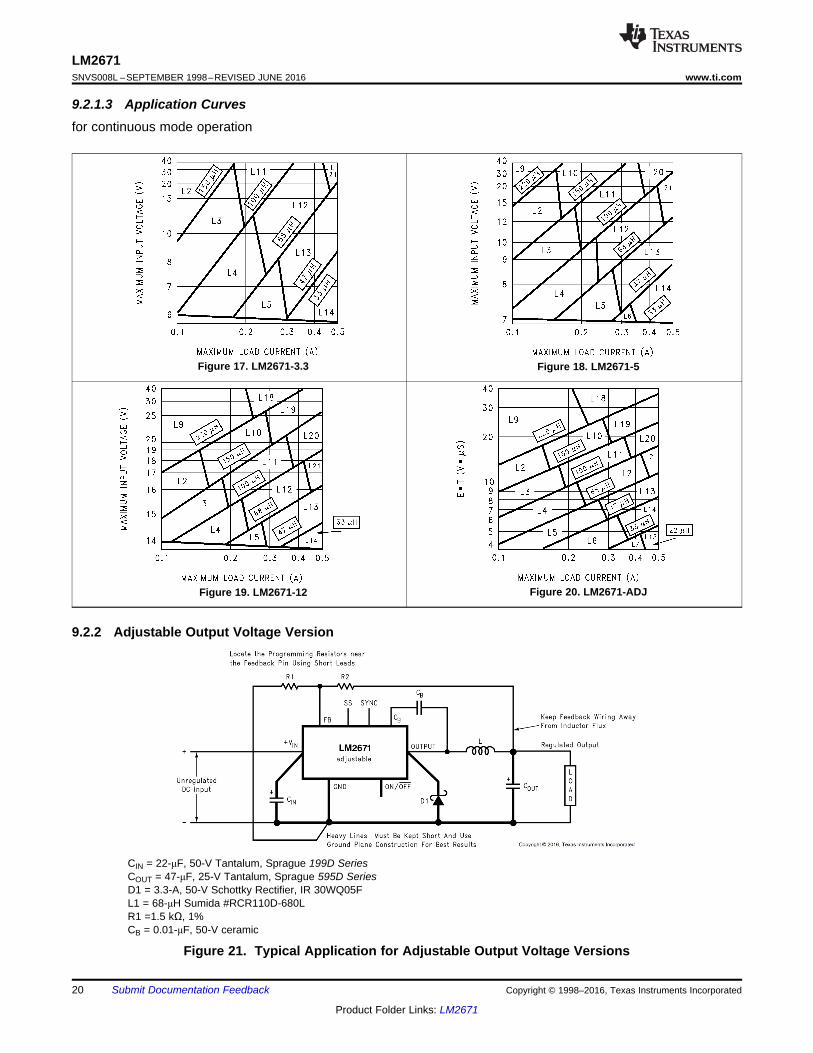
9.2.1.2.2 Output Capacitor Selection (COUT)
Select an output capacitor from the output capacitor table in Table 9. Using the output voltage and theinductance value found in the inductor selection guide, step 1, locate the appropriate capacitor value and voltagerating.
Use the 5-V section in the output capacitor table in Table 9. Choose a capacitor value and voltage rating fromthe line that contains the inductance value of 47 μH. The capacitance and voltage rating values corresponding tothe 47-μH inductor are:• Surface mount:
– 68-μF, 10-V Sprague 594D series– 100-μF, 10-V AVX TPS series
• Through hole:– 68-μF, 10-V Sanyo OS-CON SA series– 150-μF, 35-V Sanyo MV-GX series– 150-μF, 35-V Nichicon PL series– 150-μF, 35-V Panasonic HFQ series
The capacitor list contains through-hole electrolytic capacitors from four different capacitor manufacturers andsurface mount tantalum capacitors from two different capacitor manufacturers. TI recommends that both themanufacturers and the manufacturer's series that are listed in the table be used.

16
LM2671SNVS008L –SEPTEMBER 1998–REVISED JUNE 2016 www.ti.com
Product Folder Links: LM2671
Submit Documentation Feedback Copyright © 1998–2016, Texas Instruments Incorporated
Table 3. Output Capacitor Table
OUTPUTVOLTAGE
(V)INDUCTANCE
(μH)
OUTPUT CAPACITORSURFACE MOUNT THROUGH HOLE
SPRAGUE594D SERIES
(μF/V)
AVX TPSSERIES(μF/V)
SANYO OS-CONSA SERIES (μF/V)
SANYO MV-GXSERIES (μF/V)
NICHICONPL SERIES
(μF/V)
PANASONICHFQ SERIES
(μF/V)
3.3
22 120/6.3 100/10 100/10 330/35 330/35 330/3533 120/6.3 100/10 68/10 220/35 220/35 220/3547 68/10 100/10 68/10 150/35 150/35 150/3568 120/6.3 100/10 100/10 120/35 120/35 120/35
100 120/6.3 100/10 100/10 120/35 120/35 120/35150 120/6.3 100/10 100/10 120/35 120/35 120/35
5
22 100/16 100/10 100/10 330/35 330/35 330/3533 68/10 10010 68/10 220/35 220/35 220/3547 68/10 100/10 68/10 150/35 150/35 150/3568 100/16 100/10 100/10 120/35 120/35 120/35
100 100/16 100/10 100/10 120/35 120/35 120/35150 100/16 100/10 100/10 120/35 120/35 120/35
12
22 120/20 (2×) 68/20 68/20 330/35 330/35 330/3533 68/25 68/20 68/20 220/35 220/35 220/3547 47/20 68/20 47/20 150/35 150/35 150/3568 47/20 68/20 47/20 120/35 120/35 120/35
100 47/20 68/20 47/20 120/35 120/35 120/35150 47/20 68/20 47/20 120/35 120/35 120/35220 47/20 68/20 47/20 120/35 120/35 120/35
9.2.1.2.3 Catch Diode Selection (D1)1. In normal operation, the average current of the catch diode is the load current times the catch diode duty
cycle, 1-D (D is the switch duty cycle, which is approximately the output voltage divided by the input voltage).The largest value of the catch diode average current occurs at the maximum load current and maximuminput voltage (minimum D). For normal operation, the catch diode current rating must be at least 1.3 timesgreater than its maximum average current. However, if the power supply design must withstand a continuousoutput short, the diode must have a current rating equal to the maximum current limit of the LM2671. Themost stressful condition for this diode is a shorted output condition (refer to Table 4). In this example, a 1-A,20-V Schottky diode provides the best performance. If the circuit must withstand a continuous shorted output,TI recommends a higher-current Schottky diode.
2. The reverse voltage rating of the diode must be at least 1.25 times the maximum input voltage.3. Because of their fast switching speed and low forward voltage drop, Schottky diodes provide the best
performance and efficiency. This Schottky diode must be placed close to the LM2671 using short leads andshort printed-circuit traces.

17
LM2671www.ti.com SNVS008L –SEPTEMBER 1998–REVISED JUNE 2016
Product Folder Links: LM2671
Submit Documentation FeedbackCopyright © 1998–2016, Texas Instruments Incorporated
Table 4. Schottky Diode Selection Table
VR1-A DIODES 3-A DIODES
SURFACE MOUNT THROUGH HOLE SURFACE MOUNT THROUGH HOLE
20 VSK12 1N5817 SK32 1N5820B120 SR102 — SR302
30 VSK13 1N5818 SK33 1N5821B130 11DQ03 30WQ03F 31DQ03
MBRS130 SR103 — —
40 V
SK14 1N5819 SK34 1N5822B140 11DQ04 30BQ040 MBR340
MBRS140 SR104 30WQ04F 31DQ0410BQ040 — MBRS340 SR30410MQ040 — MBRD340 —15MQ040 — — —
50 VSK15 MBR150 SK35 MBR350B150 11DQ05 30WQ05F 31DQ05
10BQ050 SR105 — SR305
9.2.1.2.4 Input Capacitor (CIN)
A low ESR aluminum or tantalum bypass capacitor is required between the input pin and ground to prevent largevoltage transients from appearing at the input. This capacitor must be placed close to the IC using short leads. Inaddition, the RMS current rating of the input capacitor must be selected to be at least ½ the DC load current. Thecapacitor manufacturer data sheet must be checked to assure that this current rating is not exceeded. Thecurves shown in Figure 16 show typical RMS current ratings for several different aluminum electrolytic capacitorvalues. A parallel connection of two or more capacitors may be required to increase the total minimum RMScurrent rating to suit the application requirements.
For an aluminum electrolytic capacitor, the voltage rating must be at least 1.25 times the maximum input voltage.Caution must be exercised if solid tantalum capacitors are used. The tantalum capacitor voltage rating must betwice the maximum input voltage. Table 5 and Table 6 show the recommended application voltage for AVX TPSand Sprague 594D tantalum capacitors. TI also recommends that they be surge current tested by themanufacturer. The TPS series available from AVX, and the 593D and 594D series from Sprague are all surgecurrent tested. Another approach to minimize the surge current stresses on the input capacitor is to add a smallinductor in series with the input supply line.
Table 5. AVX TPSRECOMMENDED
APPLICATION VOLTAGEVOLTAGERATING
85°C RATING3.3 6.35 1010 2012 2515 35

18
LM2671SNVS008L –SEPTEMBER 1998–REVISED JUNE 2016 www.ti.com
Product Folder Links: LM2671
Submit Documentation Feedback Copyright © 1998–2016, Texas Instruments Incorporated
Table 6. Sprague 594DRECOMMENDED
APPLICATION VOLTAGEVOLTAGERATING
85°C RATING2.5 43.3 6.35 108 1612 2018 2524 3529 50
Use caution when using ceramic capacitors for input bypassing, because it may cause severe ringing at the VINpin. The important parameters for the input capacitor are the input voltage rating and the RMS current rating.With a maximum input voltage of 12 V, an aluminum electrolytic capacitor with a voltage rating greater than 15 V(1.25 × VIN) is required. The next higher capacitor voltage rating is 16 V.
The RMS current rating requirement for the input capacitor in a buck regulator is approximately ½ the DC loadcurrent. In this example, with a 500-mA load, a capacitor with a RMS current rating of at least 250 mA isrequired. The curves shown in Figure 16 can be used to select an appropriate input capacitor. From the curves,locate the 16-V line and note which capacitor values have RMS current ratings greater than 250 mA.
Figure 16. RMS Current Ratings for Low ESR Electrolytic Capacitors (Typical)
For a through-hole design, a 100-μF, 16-V electrolytic capacitor (Panasonic HFQ series, Nichicon PL, Sanyo MV-GX series or equivalent) would be adequate. Other types or other manufacturers' capacitors can be usedprovided the RMS ripple current ratings are adequate. Additionally, for a complete surface mount design,electrolytic capacitors such as the Sanyo CV-C or CV-BS and the Nichicon WF or UR and the NIC ComponentsNACZ series could be considered.
For surface mount designs, solid tantalum capacitors can be used, but caution must be exercised with regard tothe capacitor surge current rating and voltage rating. In this example, checking the Sprague 594D seriesdatasheet, a Sprague 594D 15-μF, 25-V capacitor is adequate.
9.2.1.2.5 Boost Capacitor (CB)
This capacitor develops the necessary voltage to turn the switch gate on fully. All applications must use a0.01-μF, 50-V ceramic capacitor. For this application, and all applications, use a 0.01-μF, 50-V ceramic capacitor.

19
LM2671www.ti.com SNVS008L –SEPTEMBER 1998–REVISED JUNE 2016
Product Folder Links: LM2671
Submit Documentation FeedbackCopyright © 1998–2016, Texas Instruments Incorporated
9.2.1.2.6 Soft-Start Capacitor (CSS) – Optional
This capacitor controls the rate at which the device starts up. The formula for the soft-start capacitor CSS isEquation 1.
where• ISS= soft-start current (4.5 μA typical)• tSS= soft-start time (selected)• VSSTH= soft-start threshold voltage (0.63 V typical)• VOUT= output voltage (selected)• VSCHOTTKY= schottky diode voltage drop (0.4 V typical)• VIN= input voltage (selected) (1)
For this application, selecting a start-up time of 10 ms and using Equation 2 for CSS.
(2)
If this feature is not desired, leave this pin open. With certain soft-start capacitor values and operating conditions,the LM2671 can exhibit an overshoot on the output voltage during turnon. Especially when starting up into noload or low load, the soft-start function may not be effective in preventing a larger voltage overshoot on theoutput. With larger loads or lower input voltages during start-up this effect is minimized. In particular, avoid usingsoft-start capacitors between 0.033 µF and 1 µF.
9.2.1.2.7 Frequency Synchronization (optional)
The LM2671 (oscillator) can be synchronized to run with an external oscillator, using the sync pin (pin 3). Bydoing so, the LM2671 can be operated at higher frequencies than the standard frequency of 260 kHz. Thisallows for a reduction in the size of the inductor and output capacitor.
As shown in the drawing below, a signal applied to a RC filter at the sync pin causes the device to synchronize tothe frequency of that signal. For a signal with a peak-to-peak amplitude of 3 V or greater, a 1-kΩ resistor and a100-pF capacitor are suitable values.
For all applications, use a 1-kΩ resistor and a 100-pF capacitor for the RC filter.
20
LM2671SNVS008L –SEPTEMBER 1998–REVISED JUNE 2016 www.ti.com
Product Folder Links: LM2671
Submit Documentation Feedback Copyright © 1998–2016, Texas Instruments Incorporated
9.2.1.3 Application Curvesfor continuous mode operation
Figure 17. LM2671-3.3 Figure 18. LM2671-5
Figure 19. LM2671-12 Figure 20. LM2671-ADJ
9.2.2 Adjustable Output Voltage Version
CIN = 22-μF, 50-V Tantalum, Sprague 199D SeriesCOUT = 47-μF, 25-V Tantalum, Sprague 595D SeriesD1 = 3.3-A, 50-V Schottky Rectifier, IR 30WQ05FL1 = 68-μH Sumida #RCR110D-680LR1 =1.5 kΩ, 1%CB = 0.01-μF, 50-V ceramic
Figure 21. Typical Application for Adjustable Output Voltage Versions

21
LM2671www.ti.com SNVS008L –SEPTEMBER 1998–REVISED JUNE 2016
Product Folder Links: LM2671
Submit Documentation FeedbackCopyright © 1998–2016, Texas Instruments Incorporated
9.2.2.1 Design RequirementsTable 7 lists the design parameters for this example.
Table 7. Design ParametersPARAMETER VALUE
Regulated output voltage, VOUT 20 VMaximum input voltage, VIN(max) 28 VMaximum load current, ILOAD(max) 500 mA
Switching frequency, F Fixed at a nominal 260 kHz
9.2.2.2 Detailed Design Procedure
9.2.2.2.1 Programming Output Voltage
Select R1 and R2, as shown in Figure 21.
Use the following formula to select the appropriate resistor values.
where• VREF = 1.21 V (3)
Select R1 to be 1 kΩ, 1%. Solve for R2.
(4)
Select a value for R1 between 240 Ω and 1.5 kΩ. The lower resistor values minimize noise pickup in the sensitivefeedback pin. For the lowest temperature coefficient and the best stability with time, use 1% metal film resistors.
(5)
R2 = 1 kΩ (16.53 − 1) = 15.53 kΩ, closest 1% value is 15.4 kΩ.
R2 = 15.4 kΩ.
9.2.2.2.2 Inductor Selection (L1)1. Calculate the inductor Volt • microsecond constant E • T (V • μs) from Equation 6.
where• VSAT = internal switch saturation voltage = 0.25 V• VD = diode forward voltage drop = 0.5 V (6)
Calculate the inductor Volt • microsecond constant (E • T) with Equation 7.
(7)2. Use the E • T value from the previous formula and match it with the E • T number on the vertical axis of the
inductor value selection guide shown in Figure 20.E • T = 21.6 (V • μs) (8)
3. On the horizontal axis, select the maximum load current in Equation 9.ILOAD(max) = 500 mA (9)
4. Identify the inductance region intersected by the E • T value and the maximum load current value. Eachregion is identified by an inductance value and an inductor code (LXX). From the inductor value selectionguide shown in Figure 20, the inductance region intersected by the 21.6 (V • μs) horizontal line and the 500-mA vertical line is 100 μH, and the inductor code is L20.
5. Select an appropriate inductor from the four manufacturer's part numbers listed in Table 2. For information

22
LM2671SNVS008L –SEPTEMBER 1998–REVISED JUNE 2016 www.ti.com
Product Folder Links: LM2671
Submit Documentation Feedback Copyright © 1998–2016, Texas Instruments Incorporated
(1) SM - Surface Mount, TH - Through Hole
on the different types of inductors, see the inductor selection in the fixed output voltage design procedure.From the table in Table 2, locate line L20, and select an inductor part number from the list of manufacturers'part numbers.
9.2.2.2.3 Output Capacitor Selection (COUT)1. Select an output capacitor from the capacitor code selection guide in Table 8. Using the inductance value
found in the inductor selection guide, step 1, locate the appropriate capacitor code corresponding to thedesired output voltage. Use the appropriate row of the capacitor code selection guide, in Table 8. For thisexample, use the 15-V to 20-V row. The capacitor code corresponding to an inductance of 100 μH is C20.
2. Select an appropriate capacitor value and voltage rating, using the capacitor code, from the output capacitorselection table in Table 9. There are two solid tantalum (surface mount) capacitor manufacturers and fourelectrolytic (through hole) capacitor manufacturers to choose from. TI recommends using the manufacturersand the manufacturer's series that are listed in the table.
From the output capacitor selection table in Table 9, choose a capacitor value (and voltage rating) thatintersects the capacitor code(s) selected in section A, C20.
The capacitance and voltage rating values corresponding to the capacitor code C20 are:– Surface mount:
– 33-μF, 25-V Sprague 594D series– 33-μF, 25-V AVX TPS series
– Through hole:– 33-μF, 25-V Sanyo OS-CON SC series– 120-μF, 35-V Sanyo MV-GX series– 120-μF, 35-V Nichicon PL series– 120-μF, 35-V Panasonic HFQ series
Other manufacturers or other types of capacitors may also be used, provided the capacitor specifications(especially the 100-kHz ESR) closely match the characteristics of the capacitors listed in the output capacitortable. See the capacitor manufacturers' data sheet for this information.
Table 8. Capacitor Code Selection Guide
CASESTYLE (1)
OUTPUTVOLTAGE (V)
INDUCTANCE (μH)22 33 47 68 100 150 220
SM and TH 1.21–2.5 — — — — C1 C2 C3SM and TH 2.5–3.75 — — — C1 C2 C3 C3SM and TH 3.75–5 — — C4 C5 C6 C6 C6SM and TH 5–6.25 — C4 C7 C6 C6 C6 C6SM and TH 6.25–7.5 C8 C4 C7 C6 C6 C6 C6SM and TH 7.5–10 C9 C10 C11 C12 C13 C13 C13SM and TH 10–12.5 C14 C11 C12 C12 C13 C13 C13SM and TH 12.5–15 C15 C16 C17 C17 C17 C17 C17SM and TH 15–20 C18 C19 C20 C20 C20 C20 C20SM and TH 20–30 C21 C22 C22 C22 C22 C22 C22
TH 30–37 C23 C24 C24 C25 C25 C25 C25
23
LM2671www.ti.com SNVS008L –SEPTEMBER 1998–REVISED JUNE 2016
Product Folder Links: LM2671
Submit Documentation FeedbackCopyright © 1998–2016, Texas Instruments Incorporated
(1) The SC series of Os-Con capacitors (others are SA series)(2) The voltage ratings of the surface mount tantalum chip and Os-Con capacitors are too low to work at these voltages.
Table 9. Output Capacitor Selection TableOUTPUT CAPACITOR
CAP.REF.
DESG.#
SURFACE MOUNT THROUGH HOLE
SPRAGUE 594DSERIES (μF/V)
AVX TPS SERIES(μF/V)
SANYO OS-CON SASERIES (μF/V)
SANYO MV-GXSERIES (μF/V)
NICHICON PLSERIES (μF/V)
PANASONIC HFQSERIES (μF/V)
C1 120/6.3 100/10 100/10 220/35 220/35 220/35C2 120/6.3 100/10 100/10 150/35 150/35 150/35C3 120/6.3 100/10 100/35 120/35 120/35 120/35C4 68/10 100/10 68/10 220/35 220/35 220/35C5 100/16 100/10 100/10 150/35 150/35 150/35C6 100/16 100/10 100/10 120/35 120/35 120/35C7 68/10 100/10 68/10 150/35 150/35 150/35C8 100/16 100/10 100/10 330/35 330/35 330/35C9 100/16 100/16 100/16 330/35 330/35 330/35C10 100/16 100/16 68/16 220/35 220/35 220/35C11 100/16 100/16 68/16 150/35 150/35 150/35C12 100/16 100/16 68/16 120/35 120/35 120/35C13 100/16 100/16 100/16 120/35 120/35 120/35C14 100/16 100/16 100/16 220/35 220/35 220/35C15 47/20 68/20 47/20 220/35 220/35 220/35C16 47/20 68/20 47/20 150/35 150/35 150/35C17 47/20 68/20 47/20 120/35 120/35 120/35C18 68/25 (2×) 33/25 47/25 (1) 220/35 220/35 220/35C19 33/25 33/25 33/25 (1) 150/35 150/35 150/35C20 33/25 33/25 33/25 (1) 120/35 120/35 120/35C21 33/35 (2×) 22/25 (2) 150/35 150/35 150/35C22 33/35 22/35 (2) 120/35 120/35 120/35C23 (2) (2) (2) 220/50 100/50 120/50C24 (2) (2) (2) 150/50 100/50 120/50C25 (2) (2) (2) 150/50 82/50 82/50
9.2.2.2.4 Catch Diode Selection (D1)1. In normal operation, the average current of the catch diode is the load current times the catch diode duty
cycle, 1-D (D is the switch duty cycle, which is approximately VOUT/VIN). The largest value of the catch diodeaverage current occurs at the maximum input voltage (minimum D). For normal operation, the catch diodecurrent rating must be at least 1.3 times greater than its maximum average current. However, if the powersupply design must withstand a continuous output short, the diode must have a current rating greater thanthe maximum current limit of the LM2671. The most stressful condition for this diode is a shorted outputcondition.
Refer to the table shown in Table 4. Schottky diodes provide the best performance, and in this example a 1-A, 40-V Schottky diode would be a good choice. If the circuit must withstand a continuous shorted output, ahigher current (at least 1.2 A) Schottky diode is recommended.
2. The reverse voltage rating of the diode must be at least 1.25 times the maximum input voltage.3. Because of their fast switching speed and low forward voltage drop, Schottky diodes provide the best
performance and efficiency. The Schottky diode must be placed close to the LM2671 using short leads andshort printed-circuit traces.

24
LM2671SNVS008L –SEPTEMBER 1998–REVISED JUNE 2016 www.ti.com
Product Folder Links: LM2671
Submit Documentation Feedback Copyright © 1998–2016, Texas Instruments Incorporated
9.2.2.2.5 Input Capacitor (CIN)
A low ESR aluminum or tantalum bypass capacitor is required between the input pin and ground to prevent largevoltage transients from appearing at the input. This capacitor must be placed close to the IC using short leads. Inaddition, the RMS current rating of the input capacitor must be selected to be at least ½ the DC load current. Thecapacitor manufacturer data sheet must be checked to assure that this current rating is not exceeded. Thecurves shown in Figure 16 show typical RMS current ratings for several different aluminum electrolytic capacitorvalues. A parallel connection of two or more capacitors may be required to increase the total minimum RMScurrent rating to suit the application requirements.
For an aluminum electrolytic capacitor, the voltage rating must be at least 1.25 times the maximum input voltage.Caution must be exercised if solid tantalum capacitors are used. The tantalum capacitor voltage rating must betwice the maximum input voltage. The Table 10 and Table 11 show the recommended application voltage forAVX TPS and Sprague 594D tantalum capacitors. TI also recommends that they be surge current tested by themanufacturer. The TPS series available from AVX, and the 593D and 594D series from Sprague are all surgecurrent tested. Another approach to minimize the surge current stresses on the input capacitor is to add a smallinductor in series with the input supply line.
Table 10. AVX TPSRECOMMENDED
APPLICATION VOLTAGEVOLTAGERATING
85°C RATING3.3 6.35 1010 2012 2515 35
Table 11. Sprague 594DRECOMMENDED
APPLICATION VOLTAGEVOLTAGERATING
85°C RATING2.5 43.3 6.35 108 1612 2018 2524 3529 50
Use caution when using ceramic capacitors for input bypassing, because it may cause severe ringing at the VINpin.
The important parameters for the input capacitor are the input voltage rating and the RMS current rating. With amaximum input voltage of 28 V, an aluminum electrolytic capacitor with a voltage rating of at least35 V (1.25 × VIN) is required.
The RMS current rating requirement for the input capacitor in a buck regulator is approximately ½ the DC loadcurrent. In this example, with a 500-mA load, a capacitor with a RMS current rating of at least 250 mA isrequired. The curves shown in Figure 22 can be used to select an appropriate input capacitor. From the curves,locate the 35-V line and note which capacitor values have RMS current ratings greater than 250 mA.

25
LM2671www.ti.com SNVS008L –SEPTEMBER 1998–REVISED JUNE 2016
Product Folder Links: LM2671
Submit Documentation FeedbackCopyright © 1998–2016, Texas Instruments Incorporated
Figure 22. RMS Current Ratings for Low ESR Electrolytic Capacitors (Typical)
For a through-hole design, a 68-μF, 35-V electrolytic capacitor (Panasonic HFQ series, Nichicon PL, Sanyo MV-GX series or equivalent) would be adequate. Other types or other manufacturers' capacitors can be usedprovided the RMS ripple current ratings are adequate. Additionally, for a complete surface mount design,electrolytic capacitors such as the Sanyo CV-C or CV-BS and the Nichicon WF or UR and the NIC ComponentsNACZ series could be considered.
For surface mount designs, solid tantalum capacitors can be used, but caution must be exercised with regard tothe capacitor surge current rating and voltage rating. In this example, checking the Sprague 594D series datasheet, a Sprague 594D 15-μF, 50-V capacitor is adequate.
9.2.2.2.6 Boost Capacitor (CB)
This capacitor develops the necessary voltage to turn the switch gate on fully. All applications must use a0.01-μF, 50-V ceramic capacitor. For this application, and all applications, use a 0.01-μF, 50-V ceramic capacitor.
If the soft-start and frequency synchronization features are desired, look at steps 6 and 7 in Detailed DesignProcedure.

26
LM2671SNVS008L –SEPTEMBER 1998–REVISED JUNE 2016 www.ti.com
Product Folder Links: LM2671
Submit Documentation Feedback Copyright © 1998–2016, Texas Instruments Incorporated
9.2.2.3 Application Curves
Continuous Mode Switching Waveforms, VIN = 20 V, VOUT = 5 V,ILOAD = 500 mA, L = 100 μH, COUT = 100 μF, COUTESR = 0.1 ΩA: VSW pin voltage, 10 V/div.B: Inductor current, 0.2 A/divC: Output ripple voltage, 50 mV/div ac-coupled
Figure 23. Horizontal Time Base: 1 μs/div
Discontinuous Mode Switching Waveforms, VIN = 20 V,VOUT = 5 V, ILOAD = 300 mA, L = 15 μH, COUT = 68 μF (2×),COUTESR = 25 mΩA: VSW pin voltage, 10 V/div.B: Inductor current, 0.5 A/divC: Output ripple voltage, 20 mV/div ac-coupled
Figure 24. Horizontal Time Base: 1 μs/div
Load Transient Response for Continuous Mode, VIN = 20 V,VOUT = 5 V, L = 100 μH, COUT = 100 μF, COUTESR = 0.1 ΩA: Output voltage, 100 mV/div, ac-coupledB: Load current: 100-mA to 500-mA load pulse
Figure 25. Horizontal Time Base: 50 μs/div
Load Transient Response for Discontinuous Mode, VIN = 20 V,VOUT = 5 V, L = 47 μH, COUT = 68 μF, COUTESR = 50 mΩA: Output voltage, 100 mV/div, ac-coupledB: Load current: 100-mA to 400-mA load pulse
Figure 26. Horizontal Time Base: 200 μs/div
10 Power Supply RecommendationsThe LM2671 is designed to operate from an input voltage supply up to 40 V. This input supply must be wellregulated and able to withstand maximum input current and maintain a stable voltage.
27
LM2671www.ti.com SNVS008L –SEPTEMBER 1998–REVISED JUNE 2016
Product Folder Links: LM2671
Submit Documentation FeedbackCopyright © 1998–2016, Texas Instruments Incorporated
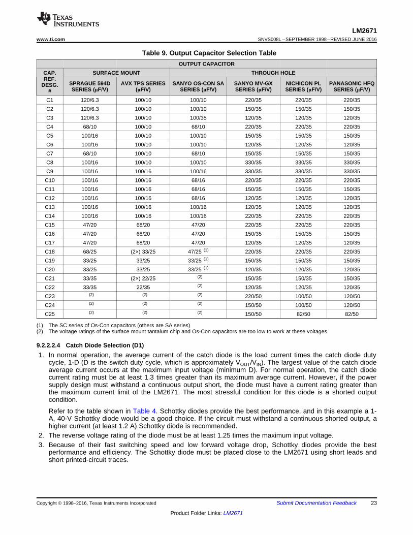
11 Layout
11.1 Layout GuidelinesLayout is very important in switching regulator designs. Rapidly switching currents associated with wiringinductance can generate voltage transients which can cause problems. For minimal inductance and groundloops, the wires indicated by heavy lines (in Figure 15 and Figure 21) must be wide printed-circuit traces andmust be kept as short as possible. For best results, external components must be placed as close to the switcherIC as possible using ground plane construction or single point grounding.
If open core inductors are used, take special care as to the location and positioning of this type of inductor.Allowing the inductor flux to intersect sensitive feedback, IC ground path, and COUT wiring can cause problems.
When using the adjustable version, take special care as to the location of the feedback resistors and theassociated wiring. Physically place both resistors near the IC, and route the wiring away from the inductor,especially an open core type of inductor.
11.2 Layout Examples
CIN = 15-μF, 25-V Solid Tantalum Sprague, 594D seriesCOUT = 68-μF, 10-V Solid Tantalum Sprague, 594D seriesD1 = 1-A, 40-V Schottky Rectifier, surface mountL1 = 47-μH, L13 Coilcraft DO3308CB = 0.01-μF, 50-V ceramic
Figure 27. Typical Surface Mount PCB Layout, Fixed Output (4x Size)
CIN = 15 μF, 50 V Solid Tantalum Sprague, 594D seriesCOUT = 33 μF, 25 V Solid Tantalum Sprague, 594D seriesD1 = 1-A, 40-V Schottky Rectifier, surface mountL1 = 100-μH, L20 Coilcraft DO3316CB = 0.01-μF, 50-V ceramicR1 = 1 kΩ, 1%R2 = Use formula in Detailed Design Procedure
Figure 28. Typical Surface Mount PCB Layout, Adjustable Output (4x Size)

28
LM2671SNVS008L –SEPTEMBER 1998–REVISED JUNE 2016 www.ti.com
Product Folder Links: LM2671
Submit Documentation Feedback Copyright © 1998–2016, Texas Instruments Incorporated
12 Device and Documentation Support
12.1 Documentation Support
12.1.1 Related DocumentationFor related documentation see the following:• AN-1187 Leadless Leadfram Package (LLP)• LM2670 SIMPLE SWITCHER® High Efficiency 3A Step-Down Voltage Regulator with Sync
12.2 Receiving Notification of Documentation UpdatesTo receive notification of documentation updates, navigate to the device product folder on ti.com. In the upperright corner, click on Alert me to register and receive a weekly digest of any product information that haschanged. For change details, review the revision history included in any revised document.
12.3 Community ResourcesThe following links connect to TI community resources. Linked contents are provided "AS IS" by the respectivecontributors. They do not constitute TI specifications and do not necessarily reflect TI's views; see TI's Terms ofUse.
TI E2E™ Online Community TI's Engineer-to-Engineer (E2E) Community. Created to foster collaborationamong engineers. At e2e.ti.com, you can ask questions, share knowledge, explore ideas and helpsolve problems with fellow engineers.
Design Support TI's Design Support Quickly find helpful E2E forums along with design support tools andcontact information for technical support.
12.4 TrademarksE2E is a trademark of Texas Instruments.SIMPLE SWITCHER, WEBENCH are registered trademarks of Texas Instruments.All other trademarks are the property of their respective owners.
12.5 Electrostatic Discharge CautionThese devices have limited built-in ESD protection. The leads should be shorted together or the device placed in conductive foamduring storage or handling to prevent electrostatic damage to the MOS gates.
12.6 GlossarySLYZ022 — TI Glossary.
This glossary lists and explains terms, acronyms, and definitions.
13 Mechanical, Packaging, and Orderable InformationThe following pages include mechanical, packaging, and orderable information. This information is the mostcurrent data available for the designated devices. This data is subject to change without notice and revision ofthis document. For browser-based versions of this data sheet, refer to the left-hand navigation.
13.1 DAP (WSON Package)The die attach pad (DAP) can and must be connected to the PCB Ground plane. For CAD and assemblyguidelines refer to AN-1187 Leadless Leadfram Package (LLP).

PACKAGE OPTION ADDENDUM
www.ti.com 16-Feb-2016
Addendum-Page 1
PACKAGING INFORMATION
Orderable Device Status(1)
Package Type PackageDrawing
Pins PackageQty
Eco Plan(2)
Lead/Ball Finish(6)
MSL Peak Temp(3)
Op Temp (°C) Device Marking(4/5)
Samples
LM2671LD-ADJ NRND WSON NHN 16 1000 TBD Call TI Call TI -40 to 125 S0008B
LM2671LD-ADJ/NOPB ACTIVE WSON NHN 16 1000 Green (RoHS& no Sb/Br)
CU SN Level-3-260C-168 HR -40 to 125 S0008B
LM2671M-12/NOPB ACTIVE SOIC D 8 95 Green (RoHS& no Sb/Br)
CU SN Level-1-260C-UNLIM -40 to 125 2671M-12
LM2671M-3.3/NOPB ACTIVE SOIC D 8 95 Green (RoHS& no Sb/Br)
CU SN Level-1-260C-UNLIM -40 to 125 2671M3.3
LM2671M-5.0 NRND SOIC D 8 95 TBD Call TI Call TI -40 to 125 2671M5.0
LM2671M-5.0/NOPB ACTIVE SOIC D 8 95 Green (RoHS& no Sb/Br)
CU SN Level-1-260C-UNLIM -40 to 125 2671M5.0
LM2671M-ADJ NRND SOIC D 8 95 TBD Call TI Call TI -40 to 125 2671MADJ
LM2671M-ADJ/NOPB ACTIVE SOIC D 8 95 Green (RoHS& no Sb/Br)
CU SN Level-1-260C-UNLIM -40 to 125 2671MADJ
LM2671MX-12/NOPB ACTIVE SOIC D 8 2500 Green (RoHS& no Sb/Br)
CU SN Level-1-260C-UNLIM -40 to 125 2671M-12
LM2671MX-3.3/NOPB ACTIVE SOIC D 8 2500 Green (RoHS& no Sb/Br)
CU SN Level-1-260C-UNLIM -40 to 125 2671M3.3
LM2671MX-5.0/NOPB ACTIVE SOIC D 8 2500 Green (RoHS& no Sb/Br)
CU SN Level-1-260C-UNLIM -40 to 125 2671M5.0
LM2671MX-ADJ/NOPB ACTIVE SOIC D 8 2500 Green (RoHS& no Sb/Br)
CU SN Level-1-260C-UNLIM -40 to 125 2671MADJ
LM2671N-12/NOPB ACTIVE PDIP P 8 40 Green (RoHS& no Sb/Br)
CU SN Level-1-NA-UNLIM -40 to 125 LM2671N-12
LM2671N-3.3/NOPB ACTIVE PDIP P 8 40 Green (RoHS& no Sb/Br)
CU SN Level-1-NA-UNLIM -40 to 125 LM2671N-3.3
LM2671N-5.0/NOPB ACTIVE PDIP P 8 40 Green (RoHS& no Sb/Br)
CU SN Level-1-NA-UNLIM -40 to 125 LM2671N-5.0
LM2671N-ADJ/NOPB ACTIVE PDIP P 8 40 Green (RoHS& no Sb/Br)
CU SN Level-1-NA-UNLIM -40 to 125 LM2671N-ADJ
(1) The marketing status values are defined as follows:ACTIVE: Product device recommended for new designs.LIFEBUY: TI has announced that the device will be discontinued, and a lifetime-buy period is in effect.

PACKAGE OPTION ADDENDUM
www.ti.com 16-Feb-2016
Addendum-Page 2
NRND: Not recommended for new designs. Device is in production to support existing customers, but TI does not recommend using this part in a new design.PREVIEW: Device has been announced but is not in production. Samples may or may not be available.OBSOLETE: TI has discontinued the production of the device.
(2) Eco Plan - The planned eco-friendly classification: Pb-Free (RoHS), Pb-Free (RoHS Exempt), or Green (RoHS & no Sb/Br) - please check http://www.ti.com/productcontent for the latest availabilityinformation and additional product content details.TBD: The Pb-Free/Green conversion plan has not been defined.Pb-Free (RoHS): TI's terms "Lead-Free" or "Pb-Free" mean semiconductor products that are compatible with the current RoHS requirements for all 6 substances, including the requirement thatlead not exceed 0.1% by weight in homogeneous materials. Where designed to be soldered at high temperatures, TI Pb-Free products are suitable for use in specified lead-free processes.Pb-Free (RoHS Exempt): This component has a RoHS exemption for either 1) lead-based flip-chip solder bumps used between the die and package, or 2) lead-based die adhesive used betweenthe die and leadframe. The component is otherwise considered Pb-Free (RoHS compatible) as defined above.Green (RoHS & no Sb/Br): TI defines "Green" to mean Pb-Free (RoHS compatible), and free of Bromine (Br) and Antimony (Sb) based flame retardants (Br or Sb do not exceed 0.1% by weightin homogeneous material)
(3) MSL, Peak Temp. - The Moisture Sensitivity Level rating according to the JEDEC industry standard classifications, and peak solder temperature.
(4) There may be additional marking, which relates to the logo, the lot trace code information, or the environmental category on the device.
(5) Multiple Device Markings will be inside parentheses. Only one Device Marking contained in parentheses and separated by a "~" will appear on a device. If a line is indented then it is a continuationof the previous line and the two combined represent the entire Device Marking for that device.
(6) Lead/Ball Finish - Orderable Devices may have multiple material finish options. Finish options are separated by a vertical ruled line. Lead/Ball Finish values may wrap to two lines if the finishvalue exceeds the maximum column width.
Important Information and Disclaimer:The information provided on this page represents TI's knowledge and belief as of the date that it is provided. TI bases its knowledge and belief on informationprovided by third parties, and makes no representation or warranty as to the accuracy of such information. Efforts are underway to better integrate information from third parties. TI has taken andcontinues to take reasonable steps to provide representative and accurate information but may not have conducted destructive testing or chemical analysis on incoming materials and chemicals.TI and TI suppliers consider certain information to be proprietary, and thus CAS numbers and other limited information may not be available for release.
In no event shall TI's liability arising out of such information exceed the total purchase price of the TI part(s) at issue in this document sold by TI to Customer on an annual basis.

TAPE AND REEL INFORMATION
*All dimensions are nominal
Device PackageType
PackageDrawing
Pins SPQ ReelDiameter
(mm)
ReelWidth
W1 (mm)
A0(mm)
B0(mm)
K0(mm)
P1(mm)
W(mm)
Pin1Quadrant
LM2671LD-ADJ WSON NHN 16 1000 178.0 12.4 5.3 5.3 1.3 8.0 12.0 Q1
LM2671LD-ADJ/NOPB WSON NHN 16 1000 178.0 12.4 5.3 5.3 1.3 8.0 12.0 Q1
LM2671MX-12/NOPB SOIC D 8 2500 330.0 12.4 6.5 5.4 2.0 8.0 12.0 Q1
LM2671MX-3.3/NOPB SOIC D 8 2500 330.0 12.4 6.5 5.4 2.0 8.0 12.0 Q1
LM2671MX-5.0/NOPB SOIC D 8 2500 330.0 12.4 6.5 5.4 2.0 8.0 12.0 Q1
LM2671MX-ADJ/NOPB SOIC D 8 2500 330.0 12.4 6.5 5.4 2.0 8.0 12.0 Q1
PACKAGE MATERIALS INFORMATION
www.ti.com 20-Sep-2016
Pack Materials-Page 1

*All dimensions are nominal
Device Package Type Package Drawing Pins SPQ Length (mm) Width (mm) Height (mm)
LM2671LD-ADJ WSON NHN 16 1000 210.0 185.0 35.0
LM2671LD-ADJ/NOPB WSON NHN 16 1000 210.0 185.0 35.0
LM2671MX-12/NOPB SOIC D 8 2500 367.0 367.0 35.0
LM2671MX-3.3/NOPB SOIC D 8 2500 367.0 367.0 35.0
LM2671MX-5.0/NOPB SOIC D 8 2500 367.0 367.0 35.0
LM2671MX-ADJ/NOPB SOIC D 8 2500 367.0 367.0 35.0
PACKAGE MATERIALS INFORMATION
www.ti.com 20-Sep-2016
Pack Materials-Page 2


MECHANICAL DATA
NHN0016A
www.ti.com
LDA16A (REV A)


IMPORTANT NOTICE
Texas Instruments Incorporated and its subsidiaries (TI) reserve the right to make corrections, enhancements, improvements and otherchanges to its semiconductor products and services per JESD46, latest issue, and to discontinue any product or service per JESD48, latestissue. Buyers should obtain the latest relevant information before placing orders and should verify that such information is current andcomplete. All semiconductor products (also referred to herein as “components”) are sold subject to TI’s terms and conditions of salesupplied at the time of order acknowledgment.TI warrants performance of its components to the specifications applicable at the time of sale, in accordance with the warranty in TI’s termsand conditions of sale of semiconductor products. Testing and other quality control techniques are used to the extent TI deems necessaryto support this warranty. Except where mandated by applicable law, testing of all parameters of each component is not necessarilyperformed.TI assumes no liability for applications assistance or the design of Buyers’ products. Buyers are responsible for their products andapplications using TI components. To minimize the risks associated with Buyers’ products and applications, Buyers should provideadequate design and operating safeguards.TI does not warrant or represent that any license, either express or implied, is granted under any patent right, copyright, mask work right, orother intellectual property right relating to any combination, machine, or process in which TI components or services are used. Informationpublished by TI regarding third-party products or services does not constitute a license to use such products or services or a warranty orendorsement thereof. Use of such information may require a license from a third party under the patents or other intellectual property of thethird party, or a license from TI under the patents or other intellectual property of TI.Reproduction of significant portions of TI information in TI data books or data sheets is permissible only if reproduction is without alterationand is accompanied by all associated warranties, conditions, limitations, and notices. TI is not responsible or liable for such altereddocumentation. Information of third parties may be subject to additional restrictions.Resale of TI components or services with statements different from or beyond the parameters stated by TI for that component or servicevoids all express and any implied warranties for the associated TI component or service and is an unfair and deceptive business practice.TI is not responsible or liable for any such statements.Buyer acknowledges and agrees that it is solely responsible for compliance with all legal, regulatory and safety-related requirementsconcerning its products, and any use of TI components in its applications, notwithstanding any applications-related information or supportthat may be provided by TI. Buyer represents and agrees that it has all the necessary expertise to create and implement safeguards whichanticipate dangerous consequences of failures, monitor failures and their consequences, lessen the likelihood of failures that might causeharm and take appropriate remedial actions. Buyer will fully indemnify TI and its representatives against any damages arising out of the useof any TI components in safety-critical applications.In some cases, TI components may be promoted specifically to facilitate safety-related applications. With such components, TI’s goal is tohelp enable customers to design and create their own end-product solutions that meet applicable functional safety standards andrequirements. Nonetheless, such components are subject to these terms.No TI components are authorized for use in FDA Class III (or similar life-critical medical equipment) unless authorized officers of the partieshave executed a special agreement specifically governing such use.Only those TI components which TI has specifically designated as military grade or “enhanced plastic” are designed and intended for use inmilitary/aerospace applications or environments. Buyer acknowledges and agrees that any military or aerospace use of TI componentswhich have not been so designated is solely at the Buyer's risk, and that Buyer is solely responsible for compliance with all legal andregulatory requirements in connection with such use.TI has specifically designated certain components as meeting ISO/TS16949 requirements, mainly for automotive use. In any case of use ofnon-designated products, TI will not be responsible for any failure to meet ISO/TS16949.
Products ApplicationsAudio www.ti.com/audio Automotive and Transportation www.ti.com/automotiveAmplifiers amplifier.ti.com Communications and Telecom www.ti.com/communicationsData Converters dataconverter.ti.com Computers and Peripherals www.ti.com/computersDLP® Products www.dlp.com Consumer Electronics www.ti.com/consumer-appsDSP dsp.ti.com Energy and Lighting www.ti.com/energyClocks and Timers www.ti.com/clocks Industrial www.ti.com/industrialInterface interface.ti.com Medical www.ti.com/medicalLogic logic.ti.com Security www.ti.com/securityPower Mgmt power.ti.com Space, Avionics and Defense www.ti.com/space-avionics-defenseMicrocontrollers microcontroller.ti.com Video and Imaging www.ti.com/videoRFID www.ti-rfid.comOMAP Applications Processors www.ti.com/omap TI E2E Community e2e.ti.comWireless Connectivity www.ti.com/wirelessconnectivity
Mailing Address: Texas Instruments, Post Office Box 655303, Dallas, Texas 75265Copyright © 2016, Texas Instruments Incorporated