TIDUEO2A | TI.com - Semiconductor company | TI.com
32
SPO2(AFE4403) ECG(ADS1292R) 5V0 Input Voltage Robert Tol bert Rechargeable battery Battery Charger + Monitor (BQ24232) 3V7@65mA DC/DC Boost (TPS61099) 5V2 LDO TPS769 5V0 DC/DC Buck (TLV62569) 3V3 LDO TLV755 3V0 3V3 3V3 LED dRV/ TX CTRL 5V0@10mA RX DIG/ANA [email protected] 3V3@75uA DVDD AVDD 3V0@250uA Battery Voltage: Nominal: 3.6V Charging Voltage: 4.2V Discharging Voltage: 2.8V 2 Electrode + RLD ECG LED TX PD RX TIDA-01614 SCLK Din Dout SPI CLK SPI Master In SPI Master Out PWDN RESET CS SPI TE RESET Pace Detection Module I2C_SCL TMP117 I2C_SDA Dout Din SCLK 3V3 @ 5mA 3V3 @ 135uA Temperature Sensor Module Pace detect CS2 CS CRG 3V3 Vba tt PGA P PGA N I2C_SCL I2C_SDA ECG Analog Output 3V3 @10mA LEDs: Battery charging indication Low battery indication MSP432P401 AVDDS CS SPI TE RESET Defib Sense Alar m Low Battery Indication SCK DIN DOUT I2C_SCL I2C_SDA ISOW7842 TRS3232 Tx1 Rx1 DIO DIO DIO DIO Pace detect DIO DIO DIO DIO DIO SIMO DIO DIO SOMI Isolated UART Vsi 3.3V @56mA Vso 3.3V@8mA 32MHz Vba tt AIO UART Tx1 Rx1 ECG Analo g o utp ut AIO MCLK 8MHz 8MHz 8MHz 2MHz 2MHz HFX IN HFXOUT Tx2 Rx2 SOMI SIMO CD74HC4040 3V3@80uA CP Q2 TMP117 3V3 @ 135uA Temperature Sensor Module I2C_SCL I2C_SDA TMP117 3V3 @ 135uA Temperature Sensor Module I2C_SCL I2C_SDA 3V3 1 TIDUEO2A – March 2019 – Revised May 2019 Submit Documentation Feedback Copyright © 2019, Texas Instruments Incorporated Multiparameter Front-End Reference Design for Vital Signs Patient Monitor Design Guide: TIDA-01614 Multiparameter Front-End Reference Design for Vital Signs Patient Monitor Description This reference design is for a multiparameter front-end of a patient monitor that measures vital sign parameters like electrocardiogram (ECG), heart rate, SpO2, and respiration. It uses biosensing front-end integrated circuits, like the AFE4403 and ADS1292R devices, to measure these parameters. It also uses three TMP117 sensors to accurately measure skin temperature. The design can interface with the pace detection module to detect the pace pulse. The design also uses an isolated UART connection to transfer data to a computer. The entire front-end subsystem runs on a rechargeable 3.7-V Lithium-ion (Li-ion) battery. Resources TIDA-01614 Design Folder AFE4403 Product Folder BQ24232 Product Folder MSP432P4011 Product Folder ADS1292R Product Folder TMP117 Product Folder TIDA-010005 Design Folder ASK Our E2E™ Experts Features • Monitors ECG, heart Rate, SpO2 %, respiration rate, and skin temperature • Uses bio-sensing front-end AFE4403 for SPO2 and heart rate measurement and ADS1292R for ECG and respiration measurement – Supports up to three LEDs and three photo- diodes with ambient subtraction to improve signal-to-noise Ratio (SNR) for SPO2 and heart measurement – Single lead ECG Measurement with RLD • Supports three 0.1 Celsius accurate sensors to measure the skin temperature • Interfaces to the pace detection module (Software- configurable cardiac pacemaker detection module reference design) to enable pacemaker detection • Enables data transfer over isolated UART interface • Runs on a one cell Li-ion rechargeable battery Applications • Medical sensor patches • Multiparameter patient monitor • Pulse oximeter • Electrocardiogram (ECG) spacer spacer An IMPORTANT NOTICE at the end of this TI reference design addresses authorized use, intellectual property matters and other important disclaimers and information.
Transcript of TIDUEO2A | TI.com - Semiconductor company | TI.com

SPO2(AFE4403)
ECG(ADS1292R)
5V0 Input Voltage
Robert Tolbert
Rechargeable battery
Battery Charger + Monitor
(BQ24232)
3V7@65mA
DC/DC Boost(TPS61099)
5V2 LDOTPS769
5V0
DC/DC Buck(TLV62569)
3V3
LDOTLV755
3V0
3V3
3V3
LED dRV/TX CTRL
5V0@10mA
RX DIG/ANA
[email protected]@75uA
DVDD AVDD
3V0@250uA
Battery Voltage:Nominal: 3.6V
Charging Voltage: 4.2VDischarging Voltage: 2.8V
2 Electrode + RLD ECG
LED TX
PD RX
TIDA-01614
SCLK
DinDout
SPI CLK
SPI Master InSPI Master Out
PWDN RESET
CS SPI TE
RESET
Pace Detection Module
I2C_SCL
TMP117
I2C_SDA
Dout Din SCLK
3V3 @ 5mA
3V3 @ 135uA
Temperature Sensor Module
Pace detect
CS2CS
CRG
3V3
Vbatt
PGAP PGANI2C_SCLI2C_SDA
ECG Analog Output
3V3 @10mA
LEDs:Battery charging indication
Low battery indication
MSP432P401
AVDDSCS
SPI TE
RESET
Defib Sense
Alarm
Low Battery Indication
SCK
DIN
DOUT
I2C_SCL
I2C_SDA
ISOW7842 TRS3232
Tx1
Rx1
DIO
DIO
DIO
DIO
Pace detect
DIO
DIO
DIO
DIO
DIO
SIMO
DIO
DIO
SOMI
Isolated UART
Vsi
3.3V@56mA
Vso
3.3V@8mA
32MHz
Vbatt AIO
UARTTx1
Rx1
ECG Analog output AIO
MCLK8MHz
8MHz
8MHz2MHz
2MHz
HFXIN
HFXOUT
Tx2
Rx2
SOMI
SIMO
CD74HC4040
3V3@80uA
CPQ2
TMP117
3V3 @ 135uA
Temperature Sensor Module
I2C_SCLI2C_SDA
TMP117
3V3 @ 135uA
Temperature Sensor Module
I2C_SCLI2C_SDA
3V3
1TIDUEO2A–March 2019–Revised May 2019Submit Documentation Feedback
Copyright © 2019, Texas Instruments Incorporated
Multiparameter Front-End Reference Design for Vital Signs Patient Monitor
Design Guide: TIDA-01614Multiparameter Front-End Reference Design for VitalSigns Patient Monitor
DescriptionThis reference design is for a multiparameter front-endof a patient monitor that measures vital signparameters like electrocardiogram (ECG), heart rate,SpO2, and respiration. It uses biosensing front-endintegrated circuits, like the AFE4403 and ADS1292Rdevices, to measure these parameters. It also usesthree TMP117 sensors to accurately measure skintemperature. The design can interface with the pacedetection module to detect the pace pulse. The designalso uses an isolated UART connection to transferdata to a computer. The entire front-end subsystemruns on a rechargeable 3.7-V Lithium-ion (Li-ion)battery.
Resources
TIDA-01614 Design FolderAFE4403 Product FolderBQ24232 Product FolderMSP432P4011 Product FolderADS1292R Product FolderTMP117 Product FolderTIDA-010005 Design Folder
ASK Our E2E™ Experts
Features• Monitors ECG, heart Rate, SpO2 %, respiration
rate, and skin temperature• Uses bio-sensing front-end AFE4403 for SPO2 and
heart rate measurement and ADS1292R for ECGand respiration measurement– Supports up to three LEDs and three photo-
diodes with ambient subtraction to improvesignal-to-noise Ratio (SNR) for SPO2 and heartmeasurement
– Single lead ECG Measurement with RLD• Supports three 0.1 Celsius accurate sensors to
measure the skin temperature• Interfaces to the pace detection module (Software-
configurable cardiac pacemaker detection modulereference design) to enable pacemaker detection
• Enables data transfer over isolated UART interface• Runs on a one cell Li-ion rechargeable battery
Applications• Medical sensor patches• Multiparameter patient monitor• Pulse oximeter• Electrocardiogram (ECG)
spacer
spacer
An IMPORTANT NOTICE at the end of this TI reference design addresses authorized use, intellectual property matters and otherimportant disclaimers and information.
System Description www.ti.com
2 TIDUEO2A–March 2019–Revised May 2019Submit Documentation Feedback
Copyright © 2019, Texas Instruments Incorporated
Multiparameter Front-End Reference Design for Vital Signs Patient Monitor
1 System Description
1.1 Introduction to Patient Monitoring SystemVital signs measure the basic body functions which help assess the general physical health of a personand give clues to identify possible disorder.
In this reference design, five primary vital signs are monitored:• ECG• Heart Rate• SPO2• Respiration rate• Skin temperature
Using this reference design, the data is transferred using an isolated UART connection to a PC or host.
1.2 Parameters Measured Using TIDA-01614In this reference design, five primary vital signs are measured.
ECG detects cardiac (heart) abnormalities by measuring the electrical activity generated by the heart as itcontracts. ECG measurement uses ECG electrodes that are placed on the chest or at the four extremities(RA = right arm, LA = left arm, RL = right leg, LL = left leg). This reference design measures ECG with athree electrode operation, including the right leg drive, which improves CMRR. ECG is measured usingTI’s bio-sensing front-end IC ADS1292R.
The ADS1292R is a low-power, multichannel, simultaneously-sampling, 24-bit deltasigma (ΔΣ), analog-to-digital converter (ADC) with integrated programmable gain amplifiers (PGAs), internal reference, and anonboard oscillator. This device integrates various ECG-specific functions that support scalable ECG,sports, and fitness applications. The devices is used in high-performance, multichannel data acquisitionsystems by powering down the ECG-specific circuitry. The ADS1292R has a highly programmablemultiplexer that measures temperature, supply, input short, and RLD. Additionally, the multiplexer lets youprogram any of the input electrodes as the patient reference drive. You can choose the PGA gain fromone of seven settings (1, 2, 3, 4, 6, 8, and 12). The ADCs in the device offer data rates from 125 SPS to 8kSPS. Communication to the device is accomplished through an SPI-compatible interface. The deviceprovides two general-purpose I/O (GPIO) pins for general use. Multiple devices synchronize using theSTART pin. The internal reference is programmed to either 2.42 V or 4.033 V. The internal oscillatorgenerates a 512-kHz clock. The versatile right leg drive (RLD) block lets you choose the average of anycombination of electrodes to generate the patient drive signal.
Lead-off detection is accomplished either by an external pullup or pulldown resistor or the internal currentsource or sink from the device. An internal AC lead-off detection feature is available. The ADS1292Rversion also includes a fully-integrated respiration impedance measurement function. See the Low-power,2-channel, 24-bit analog front-end for biopotential measurements data sheet for further details.
The ECG subcircuit is implemented with the ADS1292R IC. The ADS1292R is clocked either by aninternal oscillator that generates a 512-kHz clock, or externally through the CLK pin (pin 17). Eachclocking method has its advantages and disadvantages. Although the external clock provides highaccuracy, it requires additional external components. However, the internal clock requires fewercomponents, but it suffers from temperature-dependent performance. As mentioned in the data sheet,internal clocking is ideal for low-power, battery-operated systems. The internal oscillator is trimmed foraccuracy at room temperature. The accuracy varies over the specified temperature range. The onlypermissible external clock frequencies are 512 kHz or 2.048 MHz. The higher frequency option helps theSPI run at a higher speed. The ADS1292R uses the SPI communication interface to communicate with aMicrocontroller (MCU), MPU, or DSP.

www.ti.com System Description
3TIDUEO2A–March 2019–Revised May 2019Submit Documentation Feedback
Copyright © 2019, Texas Instruments Incorporated
Multiparameter Front-End Reference Design for Vital Signs Patient Monitor
1.3 SPO2 MonitoringOxygen binds to hemoglobin in red blood cells as it moves through the lungs. It travels throughout thebody as arterial blood. A pulse oximeter uses two light frequencies (red and infrared) to determine whatpercentage of hemoglobin is saturated with oxygen. The percentage is called blood oxygen saturation, orSpO2. It is the percentage of oxygenated hemoglobin (hemoglobin containing oxygen) compared to thetotal amount of hemoglobin in the blood (oxygenated and non-oxygenated hemoglobin). A pulse oximeteralso measures and displays the pulse rate and the SpO2 level simultaneously. The signal obtained fromthe pulse oximeter is the photoplethysmographic (PPG) signal, which shows the blood flow at theextremities. SpO2 is measured by a pulse oximeter, which is an indirect, non-invasive method. It emitsand absorbs a light wave passing through blood vessels (or capillaries) in the fingertip. A variation of thelight wave passing through the finger gives the SpO2 measurement since the degree of oxygen saturationcauses variations in the blood’s color. This value is represented by a percentage. If your pulse oximetersays 98%, then each red blood cell is made up of 98% oxygenated hemoglobin and 2% non-oxygenatedhemoglobin. Normal SpO2 values vary between 95% and 100%. Anything lower than 90% may be acause for concern.
Red and infrared (IR) lights are used to estimate the true hemoglobin oxygen saturation of arterial blood.Oxyhemoglobin (HbO2) absorbs visible and infrared IR light differently than deoxyhemoglobin (Hb), andappears bright red as opposed to the darker brown of Hb. Absorption in the arterial blood is representedby an AC signal that is superimposed on a DC signal, representing absorptions in other substances likepigmentation in tissue, venous, capillary, bone, and so forth. The cardiac-synchronized AC signal isapproximately 1% of the DC level. This value is known as the perfusion index percentage.
Equation 1 shows how to approximate the ratio of ratios and R:R = (ACrms of Red) / (DC of Red) / (ACrms of IR) / (DC of IR) (1)
Equation 2 shows the standard model for computing SpO2:% SpO2 = 110 – (25 × R) (2)
This model is often used in medical devices literature. However, accurate % SpO2 is computed based onthe empirical calibration of the ratio of ratios for the specific device.
1.4 Pace DetectionThe TIDA-01614 can be interfaced to TI's pace detection module (TIDA-010005) to identify a pacemakerpulse in the ECG waveform. It detects the pace with rise time of (30 µs–200 µs), amplitude of (8 mV–700mV), and duration of (100 µs–2000 µs).
2 Key System SpecificationsTable 1 lists the different characteristics and specifications of the TIDA-01614 board.
Table 1. Key System Specifications
CHARACTERISTICS SPECIFICATIONS
ECG One lead ECG operation with RLD. Sampling rate of 500 samples per second,supports ECG sensitivity of 100 µV
SPO2 Measurement Works in transmissive SPO2, refresh rate of 500 HzSkin Temperature Measurement Three temperature sensor with 0.1 degree accuracy
Pace pulse Rise-time (TR) measurementrange 30–200 µs
Pace pulse duration (TD) measurementrange 0.1–2 ms
Input Pace signal amplitude range 8 mV–700 mVInput Voltage (Vin) 5 V from Micro-USB

Patient Monitor
Battery Charger USB Input
Skin TemperatureSensor
PC
ECG ElectrodeSPO2 (Finger Clip)
Isolated UART
ECG
System Overview www.ti.com
4 TIDUEO2A–March 2019–Revised May 2019Submit Documentation Feedback
Copyright © 2019, Texas Instruments Incorporated
Multiparameter Front-End Reference Design for Vital Signs Patient Monitor
3 System Overview
3.1 High-Level System DescriptionTypically patient monitors are connected to the body so they can measure multiple parameters of thebody. Figure 1 shows a high-level block diagram of such a system. The system connects to the PCthrough a wired, isolated UART connection.
Figure 1. System Level Block Diagram
SPO2(AFE4403)
ECG(ADS1292R)
5V0 Input Voltage
Robert Tolbert
Rechargeable battery
Battery Charger + Monitor
(BQ24232)
3V7@65mA
DC/DC Boost(TPS61099)
5V2 LDOTPS769
5V0
DC/DC Buck(TLV62569)
3V3
LDOTLV755
3V0
3V3
3V3
LED dRV/TX CTRL
5V0@10mA
RX DIG/ANA
[email protected]@75uA
DVDD AVDD
3V0@250uA
Battery Voltage:Nominal: 3.6V
Charging Voltage: 4.2VDischarging Voltage: 2.8V
2 Electrode + RLD ECG
LED TX
PD RX
TIDA-01614
SCLK
DinDout
SPI CLK
SPI Master InSPI Master Out
PWDN RESET
CS SPI TE
RESET
Pace Detection Module
I2C_SCL
TMP117
I2C_SDA
Dout Din SCLK
3V3 @ 5mA
3V3 @ 135uA
Temperature Sensor Module
Pace detect
CS2CS
CRG
3V3
Vbatt
PGAP PGANI2C_SCLI2C_SDA
ECG Analog Output
3V3 @10mA
LEDs:Battery charging indication
Low battery indication
MSP432P401
AVDDSCS
SPI TE
RESET
Defib Sense
Alarm
Low Battery Indication
SCK
DIN
DOUT
I2C_SCL
I2C_SDA
ISOW7842 TRS3232
Tx1
Rx1
DIO
DIO
DIO
DIO
Pace detect
DIO
DIO
DIO
DIO
DIO
SIMO
DIO
DIO
SOMI
Isolated UART
Vsi
3.3V@56mA
Vso
3.3V@8mA
32MHz
Vbatt AIO
UARTTx1
Rx1
ECG Analog output AIO
MCLK8MHz
8MHz
8MHz2MHz
2MHz
HFXIN
HFXOUT
Tx2
Rx2
SOMI
SIMO
CD74HC4040
3V3@80uA
CPQ2
TMP117
3V3 @ 135uA
Temperature Sensor Module
I2C_SCLI2C_SDA
TMP117
3V3 @ 135uA
Temperature Sensor Module
I2C_SCLI2C_SDA
3V3
www.ti.com System Overview
5TIDUEO2A–March 2019–Revised May 2019Submit Documentation Feedback
Copyright © 2019, Texas Instruments Incorporated
Multiparameter Front-End Reference Design for Vital Signs Patient Monitor
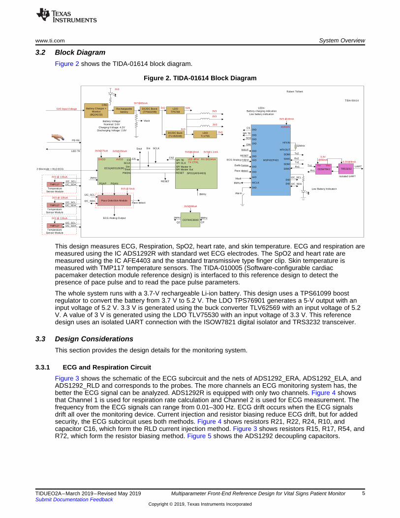
3.2 Block DiagramFigure 2 shows the TIDA-01614 block diagram.
Figure 2. TIDA-01614 Block Diagram
This design measures ECG, Respiration, SpO2, heart rate, and skin temperature. ECG and respiration aremeasured using the IC ADS1292R with standard wet ECG electrodes. The SpO2 and heart rate aremeasured using the IC AFE4403 and the standard transmissive type finger clip. Skin temperature ismeasured with TMP117 temperature sensors. The TIDA-010005 (Software-configurable cardiacpacemaker detection module reference design) is interfaced to this reference design to detect thepresence of pace pulse and to read the pace pulse parameters.
The whole system runs with a 3.7-V rechargeable Li-ion battery. This design uses a TPS61099 boostregulator to convert the battery from 3.7 V to 5.2 V. The LDO TPS76901 generates a 5-V output with aninput voltage of 5.2 V. 3.3 V is generated using the buck converter TLV62569 with an input voltage of 5.2V. A value of 3 V is generated using the LDO TLV75530 with an input voltage of 3.3 V. This referencedesign uses an isolated UART connection with the ISOW7821 digital isolator and TRS3232 transceiver.
3.3 Design ConsiderationsThis section provides the design details for the monitoring system.
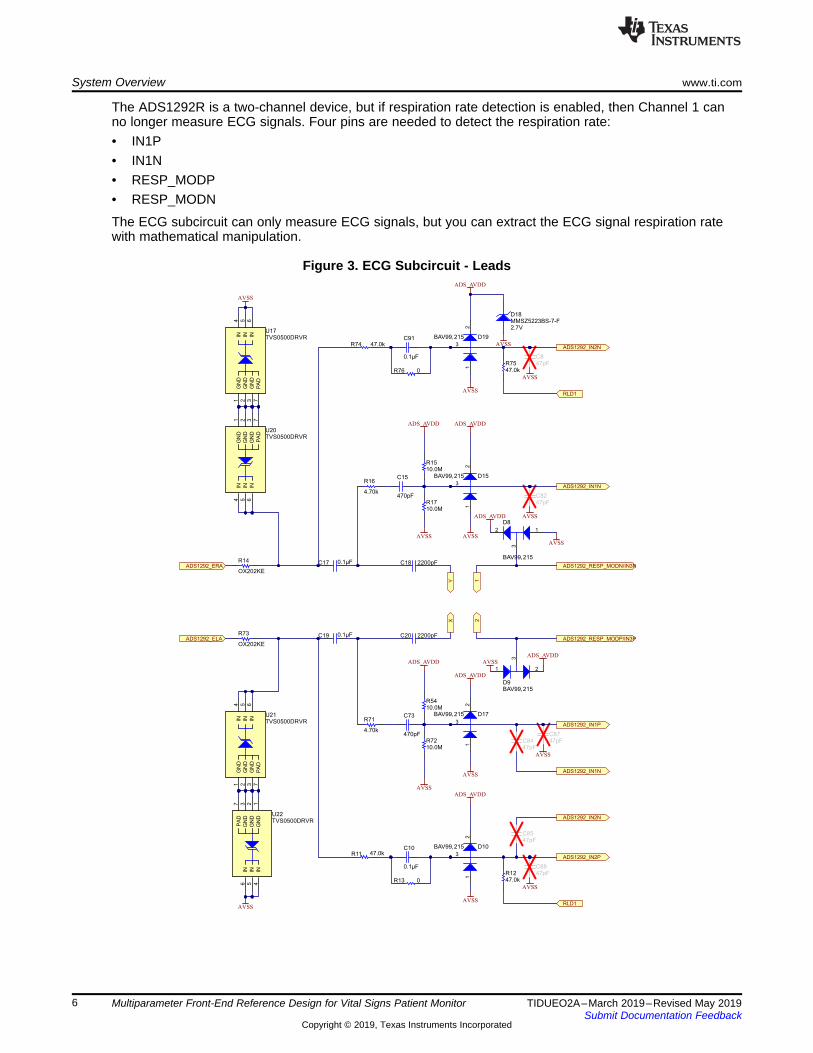
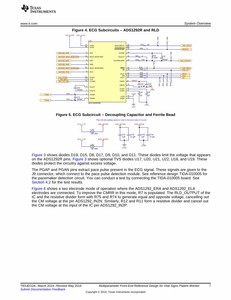
3.3.1 ECG and Respiration CircuitFigure 3 shows the schematic of the ECG subcircuit and the nets of ADS1292_ERA, ADS1292_ELA, andADS1292_RLD and corresponds to the probes. The more channels an ECG monitoring system has, thebetter the ECG signal can be analyzed. ADS1292R is equipped with only two channels. Figure 4 showsthat Channel 1 is used for respiration rate calculation and Channel 2 is used for ECG measurement. Thefrequency from the ECG signals can range from 0.01–300 Hz. ECG drift occurs when the ECG signalsdrift all over the monitoring device. Current injection and resistor biasing reduce ECG drift, but for addedsecurity, the ECG subcircuit uses both methods. Figure 4 shows resistors R21, R22, R24, R10, andcapacitor C16, which form the RLD current injection method. Figure 3 shows resistors R15, R17, R54, andR72, which form the resistor biasing method. Figure 5 shows the ADS1292 decoupling capacitors.
ADS1292_ERA
ADS1292_ELA
0.1µFC17 2200pFC18ADS1292_RESP_MODN/IN3N
470pF
C15
4.70k
R16
10.0MR17
10.0MR15
ADS_AVDD
AVSS
1
3
2
D15BAV99,215
ADS1292_IN1N
ADS_AVDD
AVSS
0.1µFC19 2200pFC20ADS1292_RESP_MODP/IN3P
470pF
C73
4.70k
R71
10.0MR72
10.0MR54
ADS_AVDD
AVSS
1
3
2
D17BAV99,215
ADS1292_IN1P
ADS_AVDD
47.0kR11
0.1µF
C10
0R13
1
3
2
D10BAV99,215
ADS1292_IN2N
ADS_AVDD
AVSS
47.0kR12
47.0kR74
0.1µF
C91
0R76
1
3
2
D19BAV99,215
ADS1292_IN2P
2.7V
D18MMSZ5223BS-7-F
ADS_AVDD
AVSS
47.0kR75
RLD1
RLD1
AVSS
AVSS
IN4
IN5
GN
D1
GN
D2
IN6
GN
D3
PA
D7
U20TVS0500DRVR
IN4
IN5
GN
D1
GN
D2
IN6
GN
D3
PA
D7
U17TVS0500DRVR
AVSS
IN4
IN5
GN
D1
GN
D2
IN6
GN
D3
PA
D7
U21TVS0500DRVR
IN4
IN5
GN
D1
GN
D2
IN6
GN
D3
PA
D7
U22TVS0500DRVR
AVSS
R14
OX202KE
R73
OX202KE
1
3
2
D8
BAV99,215
AVSS
ADS_AVDD
1
3
2
D9BAV99,215
AVSS
ADS_AVDD
47pFC84
ADS1292_IN1N
47pFC85
ADS1292_IN2N
47pFC88
AVSS
47pFC87
AVSS
47pFC82
AVSS
47pFC8
AVSS
1Y
2X
System Overview www.ti.com
6 TIDUEO2A–March 2019–Revised May 2019Submit Documentation Feedback
Copyright © 2019, Texas Instruments Incorporated
Multiparameter Front-End Reference Design for Vital Signs Patient Monitor
The ADS1292R is a two-channel device, but if respiration rate detection is enabled, then Channel 1 canno longer measure ECG signals. Four pins are needed to detect the respiration rate:• IN1P• IN1N• RESP_MODP• RESP_MODN
The ECG subcircuit can only measure ECG signals, but you can extract the ECG signal respiration ratewith mathematical manipulation.
Figure 3. ECG Subcircuit - Leads
1µFC11
0.1µFC12
1µFC13
0.1µFC14
GND
ADS_DVDD
Place the decoupling capacitor close to the power pins in Layout.
120 ohm
L19
ADS_DVDD
120 ohm
L20
ADS_AVDD
ADS_AVDDVCC_3.3V
VCC_3.0V
AVSS
PGA1N1
PGA1P2
IN1N3
IN1P4
IN2N5
IN2P6
PGA2N7
PGA2P8
VREFP9
VREFN10
VCAP111
AVDD12
AVSS13
CLKSEL14
PWDN/RESET15
START16
DGND24
DVDD23
DRDY22
DOUT21
SCLK20
DIN19
CS18
CLK17
GPIO2/RCLK225
GPIO1/RCLK126
VCAP227
RLDINV28
RLDIN/RLDREF29
RLDOUT30
RESP_MODP/IN3P31
RESP_MODN/IN3N32
U15
ADS1292RIPBS
PGAP
PGAN
ADS1292_IN1P
ADS1292_RESP_MODP/IN3P
ADS1292_IN2P
ADS1292_IN2N
ADS1292_RESP_MODN/IN3N
ADS1292_IN1N
ADS_START
ADS_CLK_SEL
ADS_AVDDADS_DVDD
1µF
C24
1µF
C25
GND
AVSS
10µFC22
0.1µFC21
AVSS
VREFP
0R460R53
0R28
Dout
Din
SCLK
0R26ADS_CS
ADS_DRDY
100kR24
0R211.00MR22
1500pF
C16
RLD_OUTPUT
0R20RESET2
0R19
10kR18ADS_GPIO1
11
TP
3
11
TP
4
11
TP
5
11
TP
61
1T
P101
1T
P9
11
TP
8
11
TP
7
XIN_MSP
AVSS
0R78
0R79 2200pFC72
2200pFC23
www.ti.com System Overview
7TIDUEO2A–March 2019–Revised May 2019Submit Documentation Feedback
Copyright © 2019, Texas Instruments Incorporated
Multiparameter Front-End Reference Design for Vital Signs Patient Monitor
Figure 4. ECG Subcircuits – ADS1292R and RLD
Figure 5. ECG Subcircuit – Decoupling Capacitor and Ferrite Bead
Figure 3 shows diodes D19, D15, D8, D17, D9, D10, and D11. These diodes limit the voltage that appearson the ADS1292R pins. Figure 3 shows optional TVS diodes U17, U20, U21, U22, U18, and U19. Thesediodes protect the circuitry against excess voltage.
The PGAP and PGAN pins extract pace pulse present in the ECG signal. These signals are given to theJ9 connector, which connect to the pace pulse detection module. See reference design TIDA-010005 forthe pacemaker detection circuit. You can conduct a test by connecting the TIDA-010005 board. SeeSection 4.2 for the test results.
Figure 6 shows a two electrode mode of operation where the ADS1292_ERA and ADS1292_ELAelectrodes are connected. To improve the CMRR in this mode, R7 is populated. The RLD_OUTPUT of theIC and the resistive divider form with R75 and R74 to generate equal and opposite voltage, cancelling outthe CM voltage at the pin ADS1292_IN2N. Similarly, R12 and R11 form a resistive divider and cancel outthe CM voltage at the input of the IC pin ADS1292_IN2P.

D
ADS1292_ERA
ADS1292_ELA
0.1µFC17 2200pFC18ADS1292_RESP_MODN/IN3N
470pF
C15
4.70k
R16
10.0MR17
10.0MR15
ADS_AVDD
AVSS
1
3
2
D15BAV99,215
ADS1292_IN1N
ADS_AVDD
AVSS
0.1µFC19 2200pFC20ADS1292_RESP_MODP/IN3P
470pF
C73
4.70k
R71
10.0MR72
10.0MR54
ADS_AVDD
AVSS
1
3
2
D17BAV99,215
ADS1292_IN1P
ADS_AVDD
47.0kR11
0.1µF
C10
0R13
1
3
2
D10BAV99,215
ADS1292_IN2N
ADS_AVDD
AVSS
47.0kR12
47.0kR74
0.1µF
C91
0R76
1
3
2
D19BAV99,215
ADS1292_IN2P
2.7V
D18MMSZ5223BS-7-F
ADS_AVDD
AVSS
47.0kR75
RLD1
RLD1
ADS1292_RLD10.0k
R9
AVSS
1
3
2
D11BAV99,215
ADS_AVDD
AVSS
0R7
RLD
1
RLD_OUTPUT10.0k
R10
PGA1N1
PGA1P2
IN1N3
IN1P4
IN2N5
IN2P6
PGA2N7
PGA2P8
VREFP9
VREFN10
VCAP111
AVDD12
AVSS13
CLKSEL14
PWDN/RESET15
START16
DGND24
DVDD23
DRDY22
DOUT21
SCLK20
DIN19
CS18
CLK17
GPIO2/RCLK225
GPIO1/RCLK126
VCAP227
RLDINV28
RLDIN/RLDREF29
RLDOUT30
RESP_MODP/IN3P31
RESP_MODN/IN3N32
U15
ADS1292RIPBS
PGAP
PGAN
ADS1292_IN1P
ADS1292_RESP_MODP/IN3P
ADS1292_IN2P
ADS1292_IN2N
ADS1292_RESP_MODN/IN3N
ADS1292_IN1N
ADS_START
ADS_CLK_SEL
AVSS
ADS_AVDDADS_DVDD
1µFC11
0.1µFC12
1µFC13
0.1µFC14
GND
ADS_DVDD
Place the decoupling capacitor close to the power pins in Layout.
120 ohm
L19
ADS_DVDD
120 ohm
L20
ADS_AVDD
ADS_AVDD
1µF
C24
1µF
C25
GND
AVSS
10µFC22
0.1µFC21
AVSS
VREFP
0R460R53
0R28
Dout
Din
SCLK
0R26ADS_CS
ADS_DRDY
100kR24
0R211.00MR22
1500pF
C16
RLD_OUTPUT
0R20RESET2
0R19
10kR18ADS_GPIO1
1
2
3
4
5
6
7
8
9
11
10
J15
ADS1292_ERA
ADS1292_ELA
ADS1292_RLD
AVSS
0.01µFC9
VCC_3.3V
VCC_3.0V
11
TP
3
11
TP
4
11
TP
5
11
TP
61
1T
P101
1T
P9
11
TP
8
11
TP
7
XIN_MSP
IN4
IN5
GN
D1
GN
D2
IN6
GN
D3
PA
D7
U20TVS0500DRVR
IN4
IN5
GN
D1
GN
D2
IN6
GN
D3
PA
D7
U17TVS0500DRVR
AVSS
IN4
IN5
GN
D1
GN
D2
IN6
GN
D3
PA
D7
U21TVS0500DRVR
IN4
IN5
GN
D1
GN
D2
IN6
GN
D3
PA
D7
U22TVS0500DRVR
AVSS
IN4
IN5
GND1
GND2
IN6
GND3
PAD7
U18
TVS0500DRVR
IN4
IN5
GND1
GND2
IN6
GND3
PAD7
U19
TVS0500DRVR
AVSS
R14
OX202KE
R73
OX202KE
R8
OX202KE
AVSS
AVSS
AVSS
AVSS
0
R68
GNDAVSS
0R78
0R79
1
3
2
D8
BAV99,215
AVSS
ADS_AVDD
1
3
2
D9BAV99,215
AVSSADS_AVDD
0
R77
47pFC84
ADS1292_IN1N
47pFC85
ADS1292_IN2N
47pFC88
AVSS
47pFC87
AVSS
47pFC82
AVSS
47pFC8
AVSS
1Y
2X
2
3
1
2
Q1BC847BW,115
3
1
2
Q2BC847BW,115
AVSS
AVSS
Y
1
3
1
2
Q3BC847BW,115
3
1
2
Q4BC847BW,115
AVSS
AVSS
X
AVSS
1µF
C86
ADS_AVDD
P4.5_A4
39k
R88
39k
R93
10.0k
R89
10.0k
R90
10.0k
R94
10.0k
R95
47
R91
470R27
470R92
2200pFC72
2200pFC23
System Overview www.ti.com
8 TIDUEO2A–March 2019–Revised May 2019Submit Documentation Feedback
Copyright © 2019, Texas Instruments Incorporated
Multiparameter Front-End Reference Design for Vital Signs Patient Monitor
Figure 6. ADS1292_ERA and ADS1292_ELA – Two-Electrode Operation
In the three electrode mode of operation, disconnect R7 and the RLD amplifier to create an equal andopposite signal, cancelling out the 50 or 60 HZ common mode signal coming from the body and improvingthe CMRR.
A 32-kHz or 64-kHz signal is sent through the R23 and R27 resistor to the right and left electrode. TheR23 and R27 resistors form a resistive divider and the body impedance of 500 Ω, which varies from 0.1 Ωto 1 Ω with respiration. The high-frequency envelope, modulated by the variation in the impedance of thebody, is fed differently through the R16 and R71 to the IC through ADS1292_IN1P and ADS1292_IN1N.Then, the envelope is demodulated and digitized to form the respiration. In this design, ADS1292R runswith an internal clock of 512 kHz.
For the ECG monitoring to be effective, the recorded ECG signals must be clean and free of noise. Anydistortion of the ECG signals from improper electrode-to-patient placement can lead to improper or misseddiagnosis. Use monitoring techniques to verify that electrodes are properly adhered to the patient. TheADS1292R offers lead-off detection, which is a built-in monitoring circuitry that constantly monitors theECG leads to ensure they are properly adhered to the patient’s skin. With the ADS1292R, lead-offdetection is implemented either by using an external pullup or pulldown resistor, or the device internalcurrent source or sink. An internal AC lead-off detection feature is also available. You do not need externalcircuitry to enable lead-off detection.
Figure 5 shows that decoupling capacitors C11, C12, C13, C14, and ferrite bead L19 and L20 havesufficient suppression to switch the noise from the 3.3 V switching power supply. Figure 10 shows that therespiration is switched off every 30 seconds, but the transistor switch keeps the pacemaker on.

MSP432P401
Oscillator
UARTISOW7842 & TRS3232
Pace DetectionModule &TMP117
SPI
24 MHz
ADS1292R & AFE4403
AFE4403
I2C
2
3
1
2
Q1BC847BW,115
3
1
2
Q2BC847BW,115
AVSS
AVSS
Y
1
3
1
2
Q3BC847BW,115
3
1
2
Q4BC847BW,115
AVSS
AVSS
X
AVSS
1µF
C86
ADS_AVDD
P4.5_A4
39k
R88
39k
R93
10.0k
R89
10.0k
R90
10.0k
R94
10.0k
R95
47
R91
470R27
470R92
www.ti.com System Overview
9TIDUEO2A–March 2019–Revised May 2019Submit Documentation Feedback
Copyright © 2019, Texas Instruments Incorporated
Multiparameter Front-End Reference Design for Vital Signs Patient Monitor
Figure 7. Electronic Switch
3.3.2 MSP432P401V
Figure 8. MCU Connections
This reference design uses the MSP432P401 microcontroller. Figure 8 shows SPI, UART, and I2Ccommunicating to the devices. ADS1292R and AFE4403 are interfaced by SPI. It is interfaced to PC usingthe UART interface. The pace detection module and temperature sensor communicates through the I2C.The microcontroller runs with the internal oscillator of 48 MHz. 24 MHz of the HSM clock is given from themicrocontroller to the AFE4403. Battery voltage is given to the IO pin of the microcontroller to indicate lowbattery voltage.
3.3.3 Timing DiagramFigure 9 shows ADS1292R and AFE4403 Read and UART transmission (AFE4403 RDY comes afterADS1292R read).

ADS_RDY ADS1293Read
ReadAFE4403
2msec
UARTTransmission
AFE_RDY
2msec
Wait untilADS1292R readcompletes
ADS_RDY ADS1293Read
ReadAFE4403
2msec
UARTTransmission
AFE_RDY
2msec
System Overview www.ti.com
10 TIDUEO2A–March 2019–Revised May 2019Submit Documentation Feedback
Copyright © 2019, Texas Instruments Incorporated
Multiparameter Front-End Reference Design for Vital Signs Patient Monitor
Figure 9. Timing Diagram – Case 1
Figure 10 shows ADS1292R and AFE4403 Read and UART transmission (AFE4403 RDY comes whilereading ADS1292).
Figure 10. Timing Diagram – Case 2
Read the temperature sensor every two seconds. Respiration is switched off and pacemaker is ON every30 seconds.
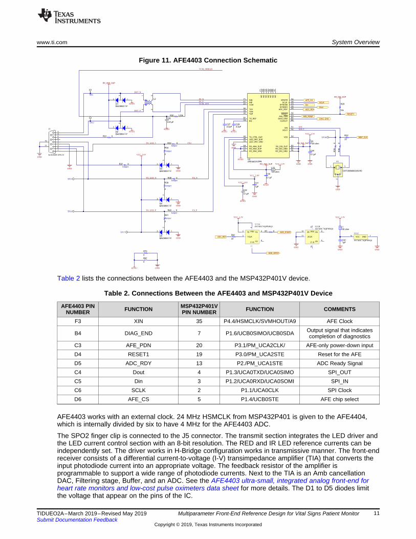
3.3.4 SPO2 MeasurementIn this reference design, SPO2 is measured using the TI bio-sensing analog front-end IC AFE4403.Figure 11 shows different connections for the AFE4403 device. The AFE4403 devices needs followingpower supplies:• RX_ANA_SUP (3.3 V)• RX_DIG_SUP (3.3 V)• LED_DRV_SUP (5 V)• TX_CTRL_SUP (5 V)
RX_ANA_SUP (3.3 V) and RX_DIG_SUP (3.3 V) are generated using the U5 IC. The L9 and L10 ferritebeads are used to suppress the switching noise from 3.3 V switching power supply. LED_DRV_SUP (5 V)and TX_CTRL_SUP (5 V) are generated using the LDO U4.
For PPG measurement, the LEDS are driven using the TXP. The TXN is used for the red LED and the IRLED and TX_LED_3 (TX_LED_3 is not used in this design) is used for the green LED. The reflectedsignals are detected using PDs connected to the INP and INN. The BG pin is connected to the internalbandgap voltage and is decoupled using 2.2 µF.
NC
A1
TX_CTRL_SUPA2
LED_DRV_GNDA3
TXNA4
TXPA5
LED_DRV_SUPA6
TX_REFB1
RX_DIG_GNDB2
TX3B3
DIAG_ENDB4
NC
B5
NC
B6
NC
C1
BGC2
AFE_PDNC3
SPISIMOC4
SPISOMIC5
SCLKC6
VCMD1
VSSD2
NC
D3
RESETD4
ADC_RDYD5
SPISTED6
INPE1
RX_ANA_GNDE2
NC
E3
RX_ANA_SUPE4
RX_DIG_SUPE5
CLKOUTE6
INNF1
RX_ANA_SUPF2
XINF3
XOUTF4
NC
F5
RX_DIG_GNDF6
U2AFE4403YZPR
2.2µFC28
2.2µFC27
GND
0.1µF
C30
VCC_3.3V
1µF
C31
GND
VCC_5.0V
0.1µF
C32
VCC_5.0V
GND
0.1µF
C29
VCC_3.3V
GND
0R
35
0R
36
22
R32TP14 MSP_CLK
AFE_CS
SCLK
Din
Dout
ADC_RDY
RESET1
10k
R29
AFE_PDNZ
DIAG_END
XINXOUT
TX30R33
0
R34
13
2
D3BAV99W-7-F GND
VCC_5.0V
TX_LED_3
0R38
0
R39
1
3
2
D4BAV99W-7-F GND
0R40
0
R41
1
3
2
D5BAV99W-7-F GND
TX_N
TX_P
TX_LED_N
TX_LED_P
TP15
TP16
1 234
L2
1.00kR30
0.01µF
C26
IN_NIN_PVCM_AFE
VCM_SHIELD
1
3
2
D2BAV99W-7-F
1
3
2
D1BAV99W-7-F
DET_N
DET_P
0R31
0R37
TP17
Jumper
Jumper
Jumper
Jumper
Jumper
Jumper
Jumper 1
2
3
Y1
CSTCE8M00G55-R0
GND
GND
GND
1
1D2
1CLK3
4
1Q5
1Q6
PRE
CLR
U11ASN74HC74QPWRQ1
10
2CLK11
2D12
13
2Q8
2Q9PRE
CLR
U11BSN74HC74QPWRQ1
VCC14
GND7
U11C
SN74HC74QPWRQ1
GNDGND
1µFC81
VCC_3.3V
22
R61
VCC_3.3V
ADC_RDY
ADS_GPIO1
ADS_START
100 ohmL1
0R1
TP2
TP12
1
2
3
4
5
6
7
8
9
11
10
J5
K202XHT-E9S-N
AVSS1 AVSS1
AVSS1
AVSS1
AVSS1
AVSS1
AVSS1
AVSS1
0
R67
GNDAVSS1
120 ohm
L10
120 ohmL9
RX_DIG_SUP
RX_DIG_SUP
RX_ANA_SUP
RX_ANA_SUP
GND
0
R70
www.ti.com System Overview
11TIDUEO2A–March 2019–Revised May 2019Submit Documentation Feedback
Copyright © 2019, Texas Instruments Incorporated
Multiparameter Front-End Reference Design for Vital Signs Patient Monitor
Figure 11. AFE4403 Connection Schematic
Table 2 lists the connections between the AFE4403 and the MSP432P401V device.
Table 2. Connections Between the AFE4403 and MSP432P401V Device
AFE4403 PINNUMBER FUNCTION MSP432P401V
PIN NUMBER FUNCTION COMMENTS
F3 XIN 35 P4.4/HSMCLK/SVMHOUT/A9 AFE Clock
B4 DIAG_END 7 P1.6/UCB0SIMO/UCB0SDA Output signal that indicatescompletion of diagnostics
C3 AFE_PDN 20 P3.1/PM_UCA2CLK/ AFE-only power-down inputD4 RESET1 19 P3.0/PM_UCA2STE Reset for the AFED5 ADC_RDY 13 P2./PM_UCA1STE ADC Ready SignalC4 Dout 4 P1.3/UCA0TXD/UCA0SIMO SPI_OUTC5 Din 3 P1.2/UCA0RXD/UCA0SOMI SPI_INC6 SCLK 2 P1.1/UCA0CLK SPI ClockD6 AFE_CS 5 P1.4/UCB0STE AFE chip select
AFE4403 works with an external clock. 24 MHz HSMCLK from MSP432P401 is given to the AFE4404,which is internally divided by six to have 4 MHz for the AFE4403 ADC.
The SPO2 finger clip is connected to the J5 connector. The transmit section integrates the LED driver andthe LED current control section with an 8-bit resolution. The RED and IR LED reference currents can beindependently set. The driver works in H-Bridge configuration works in transmissive manner. The front-endreceiver consists of a differential current-to-voltage (I-V) transimpedance amplifier (TIA) that converts theinput photodiode current into an appropriate voltage. The feedback resistor of the amplifier isprogrammable to support a wide range of photodiode currents. Next to the TIA is an Amb cancellationDAC, Filtering stage, Buffer, and an ADC. See the AFE4403 ultra-small, integrated analog front-end forheart rate monitors and low-cost pulse oximeters data sheet for more details. The D1 to D5 diodes limitthe voltage that appear on the pins of the IC.

VBUS
GND
Green
12
D6
TP21
GND
GND TS
VBUS1
D-2
D+3
ID4
GND5
678
11
10
9
J61051640001
GND
33.0R51
GND
60 ohmL5OUT
TP23
1
2
J7
B2B-PH-K-S(LF)(SN)
1 2
J1
10.0kR87
TS1
BAT2
BAT3
CE4
EN25
EN16
PGOOD7
VSS8
CHG9
OUT10
OUT11
ILIM12
IN13
TMR14
ITERM15
ISET16
EP17
U7
BQ24232RGTR
4.7µFC54
1µFC53
7.32kR50
3.09kR52
8.66kR99
56.2kR100
GND
TP18
1.05k
R55
Green
12
D13
1.05k
R49
1
2
J17
System Overview www.ti.com
12 TIDUEO2A–March 2019–Revised May 2019Submit Documentation Feedback
Copyright © 2019, Texas Instruments Incorporated
Multiparameter Front-End Reference Design for Vital Signs Patient Monitor
3.3.5 Li Ion Battery Charger
Figure 12. Li-Ion Battery Charger Using BQ24232
The following list provides details about the design:• Supply Voltage = 5 V• Charging current = 0.1 A• Input current limit, ILIM = 500 mA• Termination current = 25 mA• Safety timer duration, Fast charge = 7.5 hours• Battery temperature sense = 10 KΩ NTC (103AT-2)
How the fast charge current (ISET) is set:• RISET = [K(ISET) / ICHG]• K(SET) = 870 AΩ• RISET = R99 = [870 AΩ / 0.1 A] = 8.7 kΩ
How the input current limit (ILIM) is set:• RLIM = KILIM / I1-MAX• KILIM = 1530 AΩ• RILIM = 1530 AΩ / 0.5A = 3.06 kΩ
How the termination current threshold (ITERM, BQ24232) is set:• RITERM = RISET × ITERM × KITERM• KITERM = 0.03 A• RITERM = 8.7 kΩ × 0.025 A / 0.03 A = 7.25 kΩ
How the 7.5-hour fast-charge safety timer is set:• RTMR = tma × CHG• KTMR = 48 s / kΩ• RTMR = (7.5 hr × 3600 s/hr) / (10 × 48 s/kΩ) = 56.25 kΩ
If you are using a Li-ion battery, place a thermistor close to the battery and connect it to the Ts pin of thecharger for protection. If the temperature gets too high while it is charging, the thermistor turns off. In thisreference design, Connector J1 connects SEMITEC 103-AT-2 temperature sensor from the battery packto the Ts pin of the IC. See the USB-friendly lithium-ion batttery charger and power-path management ICdata sheet and bq24072/3/4/5/9(T) and bq24230/21.5-A single-chip li-ion and li-polymer chargemanagement IC EVM user's guide for detailed design instructions and recommendations. See TI'sWEBENCH® Design Center to generate a solution with this part.

1 2OUT REF
2
R RV V
R
u
IN1
OUT5
2
EN3
FB4
GND
U4
TPS76901DBVR
1µFC41
GND
VCC_5.2V
523kR43
169kR45
GND
VCC_5.0V
4.7uF
C35
GNDGND
TP25
GND
1µFC4
GND
VCC_3.0VVCC_3.3V
TP1OUT
5
GND2
NC4
EN3
IN1
U1
TLV75530PDBVR
10µFC47
10µFC2
10µFC3
www.ti.com System Overview
13TIDUEO2A–March 2019–Revised May 2019Submit Documentation Feedback
Copyright © 2019, Texas Instruments Incorporated
Multiparameter Front-End Reference Design for Vital Signs Patient Monitor
This reference design uses a 3.7-V Li-Ion battery. The board consumes 120 mA, so the battery runscontinuously for 4.16 hours.
3.3.6 3-V Generation Using LDO
Figure 13. 3-V Generation Using TLV5530
Figure 13 shows the LDO circuit generating 3 V from a 3.3-V input with the TLV75530. This is a fixedoutput LDO. This reference design uses a 500-mAh 3.7-V Li-ion battery. The board consumes 120 mA, sothe battery runs for 4.16 hours continuously. This circuit provides 60 mAs of current. This 3 V providessupply to the ADS1292R ADS_AVDD supply. The TLV755P device is a 500-mA low-IQ small-size low-dropout regulator, with an input voltage range of 1.45 V to 5.5 V. The device is offered in fixed outputvoltages ranging from 0.6 V to 5 V. See the Low-voltage, low-noise power supply reference design forultrasound analog front end reference design and the TLV755P 500-mA, low IQ, small size, low dropoutregulator datasheet for detailed design instructions and recommendations. See TI's WEBENCH® DesignCenter to generate a solution with this part.
3.3.7 5-V Generation Using LDO
Figure 14. 5-V Generation Using TPS76901
Figure 14 shows the LDO circuit generating 5 V from a 5.2-V input using the TPS76901. The 5 V providesthe LED_DRV_SUP and TX_CTRL_SUP of the AFE4403 IC. The TPS76901 device is an ultra-low power100-mA low-dropout linear regulator.
Output Voltage SetFigure 14 shows the output voltage from the TPS76901 adjustable regulator being programmed with anexternal resistor. Equation 3 shows how to calculate the output voltage.
where• R1 = R43 and R2 = R45• VREF = 1.16 V typ (the internal reference voltage) (3)
Gives Vo = 5 V, with R43 = 523 kΩ, R45 = 169 kΩ and Vref = 1.16.
See the Ultra-low-power 100-mA low dropout linear regulator data sheet for detailed design instructionsand recommendations. See TI's WEBENCH® Design Center to generate a solution using this part.

1 1OUT FB
2 2
R RV V 1 0.6 V 1
R R
ª º ª º u u « » « »
« » « »¬ ¼ ¬ ¼
VINA1
SWB1
GNDA2
VOUTB2
FBC2
ENC1
U3
TPS61099YFFR
150µFC34
GND
10µFC36
2.2uHL3
1286AS-H-2R2M=P2
1.05MR42
249kR44
VCC_5.2V
GND GND
10pFC33
10µFC37
10µFC38
10µFC39
22µFC40
GND GND GNDGND
TP2410.0k
R23
10.0kR25
GND
OUT
System Overview www.ti.com
14 TIDUEO2A–March 2019–Revised May 2019Submit Documentation Feedback
Copyright © 2019, Texas Instruments Incorporated
Multiparameter Front-End Reference Design for Vital Signs Patient Monitor
3.3.8 5.2-V Generation Using DC/DC Converter
Figure 15. 5.2-V Generation Using DC/DC Converter
Figure 15 shows the switching circuit generating 5.2 V using the TPS61099 from the battery voltage,VBAT. Nominal value of VBAT is 3.7 V, but this varies between 2.8 V and 4.2 V. This 5.2-V boostconverter is used as input to the LDO TPS76901 to generate 5 V for the LED_DRV_SUP andTX_CTRL_SUP of the AFE4403 IC. This 5.2 V is the input to the TLV62569, a 3.3-V generating DC/DCconverter. This converter operates with a switching frequency of 400 kHz. See the TPS61099xsynchronous boost converter with ultra-low quiscent current data sheet for detailed design information.The TPS61099 device is a Synchronous Boost Converter with Ultra-Low Quiescent Current.
Output Voltage SetThe resistor divider network of R42 and R44 sets the output voltage. The reference voltage, VREF, is 1 V.Equation 4 helps you calculate the output voltage.
where• R1 = R42 and R2 = R44 and VREF = 1 V (4)
Substituting R42, R44, and VREF in Equation 4 gives you VOUT = 5.2 V.
See the TPS61099x synchronous boost converter with ultra-low quiscent current data sheet andTPS61099 evaluation module user's guide for detailed design instructions and recommendations. See TI'sWEBENCH® Design Center to generate a solution using this part.

1 1OUT FB
2 2
R RV V 1 0.6 V 1
R R
ª º ª º u u « » « »
« » « »¬ ¼ ¬ ¼
EN1
GND2
SW3
VIN4
FB5
U5
TLV62569DBVR
4.7µFC44
VCC_5.2V
GND
453kR47
97.6kR48
GND GND
22µFC49
GND
VCC_3.3V
4.7µFC43
GND
47µFC42
GND
0.068µF
C45
10µFC50
GND
10µFC51
GND
10µFC52
GND
2.2µH
L4
TP26
www.ti.com System Overview
15TIDUEO2A–March 2019–Revised May 2019Submit Documentation Feedback
Copyright © 2019, Texas Instruments Incorporated
Multiparameter Front-End Reference Design for Vital Signs Patient Monitor
3.3.9 3.3-V Generation Using DC - DC Converter
Figure 16. 3.3-V Generation Using DC - DC Converter
Figure 16 shows the switching circuit generating 3.3 V using the TLV62569 from the 5.2-V DC/DCConverter. 3.3 V is provided to the following:• The MCU• The RX_DIG_SUP and RX_ANA_SUP supply of the AFE4403• The ADS DVDD of ADS1292R
This 3.3 V is the input to the 3 V-generating LDO TLV75530. Ferrite beads are used at each input to avoidswitching noise from the 3.3 V converter. This is designed to operate with a switching frequency of 400kHz. The TLV62569 2-A is a high efficiency synchronous buck converter in the SOT Package. See theTLV62569 2-A high efficiency synchronous buck converter in SOT package data sheet andTLV62568EVM-789 and TLV62569EVM-789 evaluation modules user's guide for detailed designinformation.
Output Voltage SetEquation 5 shows an external resistor divider setting the output voltage.
where• R1 = R47, R2 = R48 and VFB = 0.6 V (5)
Substituting R47, R48, and VFB in Equation 5 gives you Vout = 3.3 V.
See the Ultralow-power 100-mA low dropout linear regulator data sheet and TLV62568EVM-789 andTLV62569EVM-789 evaluation modules user's guide for detailed design information.
3.3.10 Isolated UARTThis reference design provides an isolated UART connection for the wired environment. The U8 ICISOW7821DWER is the isolator and U9, TRS3232DWR, is the UART transceiver. The J16 connectorconnects to the PC with an isolated UART if the voltage is 3.3 V. The J2 connector provides the UARTRX1 and TX1 without isolation. The J16 connector provides an isolated UART TX and RX.
1
3
5 6
4
2
7
9 10
8
J9
PPTC052LFBN-RC
VCC_3.3V
I2C_SCL
I2C_SDA
Pace_Detect
GND
PGAP
PGAN
Analog_Output1
100 ohmL18
0R5
VCC_3.0V
0R6
Pace_Reset
10µFC92
GND
IO
10µFC59
1µFC61
0.1µFC63
10µFC60
1µFC62
0.1µFC64
VCC_ISO_3.3V
TX1
RX1
GND1
T1_OUTR1_IN
GND1
1
2
3
4
5
6
7
8
9
11
10
J10
K202XHT-E9S-N
220R69
EN17
GND12
GND18
GND29
GND215
INA3
INB13
NC5
NC6
NC10
NC12
OUTA14
OUTB4
SEL11
VCC1
VISO16
U8
ISOW7821DWER
1
2
3
J2
5-146278-3
GND
TX1
RX1
ISO_TX1
1
2
3
J16
5-146278-3
GND1
6.3V0.1uF
C76
C1+1
V+2
C1-3
C2+4
C2-5
V-6
DOUT27
RIN28
ROUT29
DIN210
DIN111
ROUT112
RIN113
DOUT114
GND15
VCC16
U6
TRS3232EIPW
220R63
VCC_3.3V
VCC_ISO_3.3V
0.1µFC55
0.1µFC58 0.1µF
C57
0.1µFC56
ISO_RX1
ISO_TX1ISO_RX1
12
3 4
100uH
L11
GND
1 2
34
100uH
L21
GND1
100R64
100 ohmL22
100 ohmL23
100R96
System Overview www.ti.com
16 TIDUEO2A–March 2019–Revised May 2019Submit Documentation Feedback
Copyright © 2019, Texas Instruments Incorporated
Multiparameter Front-End Reference Design for Vital Signs Patient Monitor
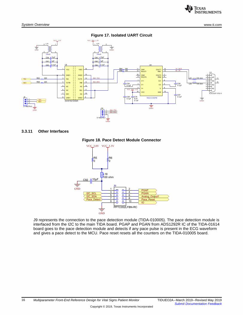
Figure 17. Isolated UART Circuit
3.3.11 Other Interfaces
Figure 18. Pace Detect Module Connector
J9 represents the connection to the pace detection module (TIDA-010005). The pace detection module isinterfaced from the I2C to the main TIDA board. PGAP and PGAN from ADS1292R IC of the TIDA-01614board goes to the pace detection module and detects if any pace pulse is present in the ECG waveformand gives a pace detect to the MCU. Pace reset resets all the counters on the TIDA-010005 board.

25V
0.1uF
C1
SDA
SCL
ADD0
ADD0
6.98k
R2
6.98k
R1100 ohm
L1
SCL
2ALERT
4
V+
SDA
U1
TMP117AIDRVR
2
4
6
8
10
J1
20021121-00010C4LF
L15
VCC_3.3V
GND
I2C_SDA
I2C_SCL
L16
VCC_3.3V
GND
I2C_SDA
I2C_SCL
L17
VCC_3.3V
GND
I2C_SDA
I2C_SCL5
4
1
2
3
J3
PEC05SAAN
5
4
1
2
3
J4
PEC05SAAN
5
4
1
2
3
J13
PEC05SAAN
www.ti.com System Overview
17TIDUEO2A–March 2019–Revised May 2019Submit Documentation Feedback
Copyright © 2019, Texas Instruments Incorporated
Multiparameter Front-End Reference Design for Vital Signs Patient Monitor
Figure 19. Temperature Connector Sensor
Figure 19 shows the connection to the temperature sensor TMP117. Three TMP117 temperature sensorsare used for accurate measurement. Interface is from the I2C to the MCU. ADD0 pin is the fifth pin andconnects to GND, V1, and SDA lines to select the unique slave address.
3.3.12 Temperature Sensor BoardFigure 20 shows the temperature sensor circuit. The TMP117 is a low-power, high-precision temperaturesensor that provides a 16-bit temperature result, with a resolution of 7.8125 m°C, and an accuracy up to±0.1°C with no calibration. The TMP117 operates from 1.8 V to 5.5 V, usually consuming 3.5 µA, andcomes in a 2.00 mm × 2.00 mm WSON package. The device also features integrated EEPROM. Threesuch boards are interfaced to the main TIDA-01614 board to have accurate temperature. Sensor isinterfaced through I2C. This design patch operates on a 3.3-V and uses a 2-layer flex PCB to reducethermal mass and maximize board flexibility. The primary benefit of flexibility is the ease and comfort forthe wearers, which improves the likelihood that the patch remains static on the patient.
U1 is the TMP117 IC and J1 is the connector that interfaces to the TIDA-01614 main board.
Figure 20. Temperature Sensor Circuit
3.3.13 TI DevicesAFE4403The AFE4403 is a fully-integrated analog front-end (AFE) supports pulse oximeter applications. Thedevice consists of a low-noise receiver channel with an integrated analog-to-digital converter (ADC), anLED transmit section, and diagnostics for sensor, and LED fault detection. The device is a configurabletiming controller. This flexibility enables the user to have complete control of the device timingcharacteristics. To ease clocking requirements and provide a low-jitter clock to the AFE4403, an oscillatoris integrated from an external crystal. The device communicates to an external microcontroller or hostprocessor using an SPI interface. The device is a complete AFE solution packaged in a single, compactDSBGA-36 (3.07-mm × 3.07-mm × 0.5-mm) and is specified over the operating temperature range of–20°C to 70°C.

System Overview www.ti.com
18 TIDUEO2A–March 2019–Revised May 2019Submit Documentation Feedback
Copyright © 2019, Texas Instruments Incorporated
Multiparameter Front-End Reference Design for Vital Signs Patient Monitor
TLV755PThe TLV755P is an ultra-small, low quiescent current, low-dropout regulator (LDO) that sources 500 mAwith good load and line transient performance. The TLV755P is optimized for a wide variety of applicationsby supporting an input voltage range from 1.45 V–5.5 V. To minimize cost and solution size, the device isoffered in fixed output voltages ranging from 0.6 V to 5 V to support the lower core voltages of modernMCUs. Additionally, the TLV755P has a low-IQ with enable functionality to minimize standby power. Thisdevice features an internal soft-start to lower inrush current, providing a controlled voltage to the load andminimizing the input voltage drop during start up. When shutdown, the device actively pulls down theoutput to quickly discharge the outputs and ensure a known start-up state.
The TLV755P is stable with small ceramic output capacitors allowing for a small overall solution size. Aprecision band-gap and error amplifier provides a typical accuracy of 1%. All device versions haveintegrated thermal shutdown, current limit, and undervoltage lockout (UVLO). The TLV755P has aninternal foldback current limit that helps reduce the thermal dissipation during short-circuit events.
TPS61099The TPS61099x device is a synchronous boost converter with 1-µA ultra-low quiescent current. Thedevice is designed for products powered by an alkaline NiMH rechargeable battery, Lithium-Mn battery, orrechargeable Li-ion battery, for which high efficiency under light load condition is critical to achieve longbattery life operation. The TPS61099x boost converter uses a hysteretic control topology to obtainmaximal efficiency at minimal quiescent current. It only consumes 1-µA quiescent current under a lightload condition and can achieve up to 75% efficiency at 10-µA load with fixed output voltage version. It canalso support up to 300-mA output current from 3.3 V–5 V conversion, and achieve up to 93% at 200-mAload.
The TPS61099x also offers Down Mode and Pass-Through operations for different applications. In DownMode, the output voltage can still be regulated at target values even when input voltage is higher thanoutput voltage. In Pass-Through Mode, the output voltage follows input voltage. The TPS61099x exitsDown Mode and enters into Pass-Through Mode when VIN > VOUT + 0.5 V. The TPS61099x supportstrue shutdown function when it is disabled, which disconnects the load from the input supply to reduce thecurrent consumption. The TPS61099x offers both adjustable output voltage version and fixed outputvoltage versions. It is available in 6-ball 1.23-mm × 0.88-mm WCSP package and 6-pin 2-mm × 2-mmWSON package.
TPS76901The TPS76901 low-dropout (LDO) voltage regulator offers the benefits of low-dropout voltage, ultra-lowpower operation, and miniaturized packaging. This regulator features low-dropout voltages and ultra-lowquiescent current compared to conventional LDO regulators. The TPS76901 device is ideal formicropower operations and where board space is at a premium.
A combination of new circuit design and process innovation has enabled the usual PNP pass transistor tobe replaced by a PMOS pass element. Because the PMOS pass element behaves as a low-value resistor,the dropout voltage is extremely low, and is directly proportional to the load current. Since the PMOS passelement is a voltage-driven device, the quiescent current is ultra-low (28 µA maximum) and is stable overthe entire range of output load current (0 mA to 100 mA). It is intended for use in portable systems suchas laptops and cellular phones. The ultra-low dropout voltage feature and ultra-low power operation resultin a significant increase in system battery operating life. The TPS76901 also features a logic-enabledsleep mode to shut down the regulator, reducing quiescent current to 1 μA, which is typical at TJ = 25°C.The TPS76901 is a variable version programmable over the range of 1.2 V–4.5 V.
TLV62569The TLV62569 device is a synchronous step-down buck DC/DC converter, optimized for high efficiencyand compact solution size. The device integrates switches capable of delivering an output current up to 2A. At medium to heavy loads, the device operates in pulse width modulation (PWM) mode with 1.5-MHzswitching frequency. At light loads, the device automatically enters Power Save Mode (PSM) to maintainhigh efficiency over the entire load current range. In shutdown, the current consumption is reduced to lessthan 2 µA. The TLV62569 provides an adjustable output voltage through an external resistor divider. Aninternal soft start circuit limits the inrush current during startup. Other features like overcurrent protection,thermal shutdown protection, and power good are built-in. The device is available in a SOT23 andSOT563 package.

www.ti.com System Overview
19TIDUEO2A–March 2019–Revised May 2019Submit Documentation Feedback
Copyright © 2019, Texas Instruments Incorporated
Multiparameter Front-End Reference Design for Vital Signs Patient Monitor
BQ24232The BQ2423x devices are highly-integrated Li-ion linear chargers and system power-path managementdevices targeted to space-limited portable applications. The devices operate from either a USB port or ACadapter, and support charge currents between 25 mA and 500 mA. The high-input-voltage range withinput overvoltage protection supports low-cost, unregulated adapters. The USB input current limit accuracyand start-up sequence let the BQ2423x meet the USB-IF inrush current specification. Additionally, theinput dynamic power management (VIN-DPM) prevents the charger from crashing poorly-designed orincorrectly-configured USB sources.
The BQ2423x features dynamic power-path management (DPPM) that powers the system whilesimultaneously and independently charging the battery. The DPPM circuit reduces the charge currentwhen the input current limit causes the system output to fall to the DPPM threshold, thus supplying thesystem load at all times while monitoring the charge current separately. This feature reduces the numberof charge and discharge cycles on the battery, allows proper charge termination, and enables the systemto run with a defective or absent battery pack. Additionally, this enables the system to instantly turn on,even with a totally discharged battery. The power-path management architecture also permits the batteryto supplement the system current requirements when the adapter cannot deliver the peak systemcurrents, enabling the use of a smaller adapter.
The battery is charged in three phases: conditioning, constant current, and constant voltage. In all chargephases, an internal control loop monitors the IC junction temperature and reduces the charge current if theinternal temperature threshold is exceeded. The charger power stage and charge current sense functionsare fully-integrated. The charger function has high-accuracy current and voltage regulation loops, chargestatus display, and charge termination. The input current limit and charge current are programmable usingexternal resistors.
ADS1292RThe ADS1292R is a multichannel, simultaneous sampling, 24-bit, delta-sigma (ΔΣ) analog-to-digitalconverters (ADCs) with a built-in programmable gain amplifier (PGA), internal reference, and an onboardoscillator. The ADS1292R incorporates all features commonly required in portable, low-power medicalECG, sports, and fitness applications.
With high levels of integration and exceptional performance, the ADS1292R enables the creation ofscalable medical instrumentation systems at significantly reduced size, power, and overall cost. TheADS1292R has a flexible input multiplexer per channel that can be independently connected to theinternally-generated signals for test, temperature, and lead-off detection. Additionally, any configuration ofinput channels can be selected for derivation of the right leg drive (RLD) output signal. ADS1292Roperates at data rates up to 8 kSPS. Lead-off detection can be internally implemented to the device, usingthe internal excitation current sink/source from the device. The ADS1292R also includes a fully-integratedrespiration impedance measurement function. The devices are packaged in a 5-mm × 5-mm, 32-pin thinquad flat pack (TQFP). Operating temperature is specified from –40°C to +85°C.
TVS0500The TVS0500 robustly shunts up to 43 A of IEC 61000-4-5 fault current to protect systems from high-power transients or lightning strikes. The device offers a solution to the common industrial signal line EMCrequirement to survive up to 2 kV IEC 61000-4-5 open circuit voltage coupled through a 42 Ω impedance.The TVS0500 uses a unique feedback mechanism to ensure precise flat-clamping during a fault, assuringsystem exposure below 10 V. The tight voltage regulation lets designers confidently select systemcomponents with a lower voltage tolerance, lowering system costs and complexity without sacrificingrobustness. In addition, the TVS0500 is available in a small 2-mm × 2-mm SON footprint, which is ideal forspace-constrained applications. It offers a 70 percent reduction in size compared to industry standardSMA and SMB packages. The extremely-low device leakage and capacitance ensure a minimal effect onthe protected line. To ensure robust protection over the lifetime of the product, TI tests the TVS0500against 5000 repetitive surge strikes at high-temperatures with no shift in device performance.
MSP432P4011The SimpleLink™ MSP432P401x MCUs are optimized host MCUs with an integrated 16-bit precisionADC. These MCUs deliver ultra-low power performance including 80 µA/MHz in active power and 660 nAin standby power with FPU and DSP extensions. As an optimized host MCU, the MSP432P401x letsdevelopers add high-precision analog and memory extension to applications based on SimpleLinkconnectivity solutions.

System Overview www.ti.com
20 TIDUEO2A–March 2019–Revised May 2019Submit Documentation Feedback
Copyright © 2019, Texas Instruments Incorporated
Multiparameter Front-End Reference Design for Vital Signs Patient Monitor
The MSP432P401x devices are part of the SimpleLink MCU platform, consisting of Wi-Fi®, Bluetooth®low-energy, Sub-1 GHz, and host MCUs. These share a common, easy-to-use development environmentwith a single core software development kit (SDK) and rich tool set. A one-time integration of theSimpleLink platform lets you add any combination of devices from the portfolio into your design. Theultimate goal of the SimpleLink platform is to achieve 100% code reuse when your design requirementschange. For more information, see the SimpleLink website.
MSP432P401x devices are supported by a comprehensive ecosystem of tools, software, documentation,training, and support to get your development started quickly. The MSP-EXP432P401R LaunchPaddevelopment kit or MSP-TS432PZ100 target socket board (with additional MCU sample) along with thefree SimpleLink MSP432 SDK is all you need to get started.

JTAG Connector (J8)
Pace Detection Module Connector
(J9)
Temperature Sensors Expansion Slot for BLE/WiFi/ Sub 1 GHz
(J11 and J2)
Battery Connector (J7)
InputPower (J6)
SPO2 Finger Clip Connector (J5)
ECG Electrode Connector (J15)
UART Connector (J10)
www.ti.com Hardware, Software, Testing Requirements, and Test Results
21TIDUEO2A–March 2019–Revised May 2019Submit Documentation Feedback
Copyright © 2019, Texas Instruments Incorporated
Multiparameter Front-End Reference Design for Vital Signs Patient Monitor
4 Hardware, Software, Testing Requirements, and Test Results
4.1 Required Hardware and Software
4.1.1 HardwareHardware connectionFigure 21 and Figure 22 show top and bottom views of the TIDA-01614 PCB.
Figure 21. TIDA-01614 PCB Connector Configuration – Top View
Figure 22. TIDA-01614 PCB Connector Configuration – Bottom View
The following list provides information about each part:• Input Power Connector (J6): A USB-connector for 5-V input power 5 V. 5 V is derived from the USB
Vbus.• Battery Connector (J7): This pin connects the rechargeable 3.7-V Lithium-ion battery.

ECG Simulator
ECG ElectrodeConnector
(J15) 3.7 Li-ion Battery
JTAG Cable
SPO2 Finger Clip MSP432 LaunchPad
UART to USB Dongle
Temperature Sensors
Hardware, Software, Testing Requirements, and Test Results www.ti.com
22 TIDUEO2A–March 2019–Revised May 2019Submit Documentation Feedback
Copyright © 2019, Texas Instruments Incorporated
Multiparameter Front-End Reference Design for Vital Signs Patient Monitor
• UART Connector (J10): This connector is given as a provision to connect to the PC through serialport.
• ECG Electrode Connector (J15): This pin connects the ECG electrodes in 2 electrode and 3electrode operations.
• Temperature Sensor Connector (J3,J4 and J13): These connectors connect the three temperaturesensors.
• SPO2 Finger Clip Connector (J5): This connector connects the SPO2 finger clip.• Expansion Slot for BLE/WiFi/Sub 1 GHz (J11 and J12): These connectors are the expansion slot for
BLE/WiFi/Sub 1 GHz.• JTAG Connector (J8): The JTAG connector is for programming.• Pace Detection Module connector (J9): This connector connects the pace detection Module (TIDA-
010005).• Isolated UART connector (J16) : This connector is used to give the provision to have 3.3 V isolated
UART signals. Connect the USB to UART Dongle (C232HD-DDHSP-0) from this connector to the PC.
4.1.2 Test SetupFigure 23 shows the test setup. An ECG simulator (Datrend AMPS-1 Advanced Modular PatientSimulator) generates ECG, Respiration, and pace signal for testing. The TIDA-01614 board isprogrammed using the MSP432 launch pad, connecting to the PC. Three temperature sensor Flex PCBsare connected to this board. Flexi PCB can be easily strapped on to the human board for temperaturemeasurement. Three such temperature sensors are used for accurate temperature measurement. ThreeECG electrodes connected to the right arm, left arm, and right leg attach to this board using J15connector. The system runs with a rechargeable 3.7-V 500 mAh Li-ion battery connected to J7 connector.C232HD – DDHSP-0 UART to USB serial cable is used for UART communication to the PC and GUI.
Figure 23. TIDA-01614 Test Setup

www.ti.com Hardware, Software, Testing Requirements, and Test Results
23TIDUEO2A–March 2019–Revised May 2019Submit Documentation Feedback
Copyright © 2019, Texas Instruments Incorporated
Multiparameter Front-End Reference Design for Vital Signs Patient Monitor
4.1.3 SoftwareThe following software tools are used to test and obtain the results for this TI reference design:• Code Composer Studio™, version 8 or higher. This software must be installed with MSP432P401
support.• SimpleLink-MSP432P401-SDK Software. You can download it at http://www.ti.com/tool/simplelink-
msp432-sdk.• GUI Composer Run Time Engine. You can download it at http://software-dl.ti.com/ccs/non-
esd/gui_composer/runtime/gcruntime-7.0.0-windows-installer.exe .
The following instructions assume that Code Composer Studio is installed on the PC. Download the GUIComposer application setup (zip file) and TIDA-01614 firmware (zip file) from the TIDA-01614 productpage. Follow these instructions to download the software loading for the TIDA-01614 board:1. Plug in the MSP EXP432P401R board on the USB port of the PC. Section 4.1.2 shows the setup.
Table 2 lists the connections between the TIDA-01614 board and the MSP EXP432P401R) board.2. Open Code Composer Studio as administrator.
a. Right click on the CCS icon and run as administrator.3. Click on the Project option in the main toolbar.4. Click Import CCS projects.5. Select the installed firmware (Default: C:\Program Files (x86)\Texas Instruments\TIDA01614\TIDA-
01614_firmware).6. Import all projects.7. Click the OK button.8. Click View.9. Click Project Explorer.10. Select TIDA-01614 firmware.11. Click on the Run and Debug buttons, which program the board with the selected project file.
Go to https://dev.ti.com/gallery/info/5331888/med_tida01614/ver/1.0.1/ for the GUI composer. You mustuse Google Chrome to open the link. Use the following steps for the GUI composer.
Figure 24. Step 1
1. Click anywhere inside the card. A pop-up appears to download and install the TI cloud agent. Install itand click to finish.

Hardware, Software, Testing Requirements, and Test Results www.ti.com
24 TIDUEO2A–March 2019–Revised May 2019Submit Documentation Feedback
Copyright © 2019, Texas Instruments Incorporated
Multiparameter Front-End Reference Design for Vital Signs Patient Monitor
Figure 25. Step 2
2. Click on the Quick Start button.
Figure 26. Step 3
3. Go to the Options tab.4. Select 460800 as the baud rate and select the COM port for the USB to UART Dongle.5. Click on the Start Monitoring button. Ensure that it shows that the hardware is connected on the bottom
panel.
www.ti.com Hardware, Software, Testing Requirements, and Test Results
25TIDUEO2A–March 2019–Revised May 2019Submit Documentation Feedback
Copyright © 2019, Texas Instruments Incorporated
Multiparameter Front-End Reference Design for Vital Signs Patient Monitor
4.2 Test Results
4.2.1 Test Results
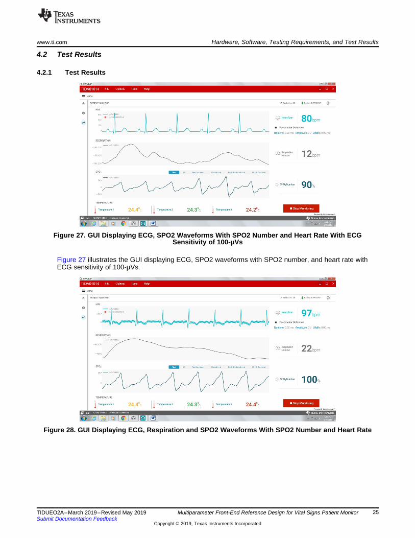
Figure 27. GUI Displaying ECG, SPO2 Waveforms With SPO2 Number and Heart Rate With ECGSensitivity of 100-µVs
Figure 27 illustrates the GUI displaying ECG, SPO2 waveforms with SPO2 number, and heart rate withECG sensitivity of 100-µVs.
Figure 28. GUI Displaying ECG, Respiration and SPO2 Waveforms With SPO2 Number and Heart Rate

Hardware, Software, Testing Requirements, and Test Results www.ti.com
26 TIDUEO2A–March 2019–Revised May 2019Submit Documentation Feedback
Copyright © 2019, Texas Instruments Incorporated
Multiparameter Front-End Reference Design for Vital Signs Patient Monitor
Figure 29. GUI Showing the Pacemaker Detection
Figure 29 illustrates the GUI showing the pacemaker detection. This result is captured with the respirationoff.
Figure 30. Output Ripple Voltage of 5.2 V Supply for Input Voltage of 3.7 V, and Input Current of 120 mA
Figure 30 shows the output ripple voltage of 5.2 V supply with input voltage of 3.7 V, and input current of120 mA.

www.ti.com Hardware, Software, Testing Requirements, and Test Results
27TIDUEO2A–March 2019–Revised May 2019Submit Documentation Feedback
Copyright © 2019, Texas Instruments Incorporated
Multiparameter Front-End Reference Design for Vital Signs Patient Monitor
Figure 31. Output Ripple Voltage of 5 V Supply for Input Voltage of 3.7 V, and Input Current of 120 mA
Figure 31 shows the output ripple voltage of 5 V supply for input voltage of 3.7 V, and input current of 120mA.
Figure 32. Output Ripple Voltage of 3.3 V Supply for Input Voltage of 3.7 V, and Input Current of 120 mA
Figure 32 shows the output ripple voltage of 3.3 V supply for input voltage of 3.7 V, and input current of120 mA.
Hardware, Software, Testing Requirements, and Test Results www.ti.com
28 TIDUEO2A–March 2019–Revised May 2019Submit Documentation Feedback
Copyright © 2019, Texas Instruments Incorporated
Multiparameter Front-End Reference Design for Vital Signs Patient Monitor
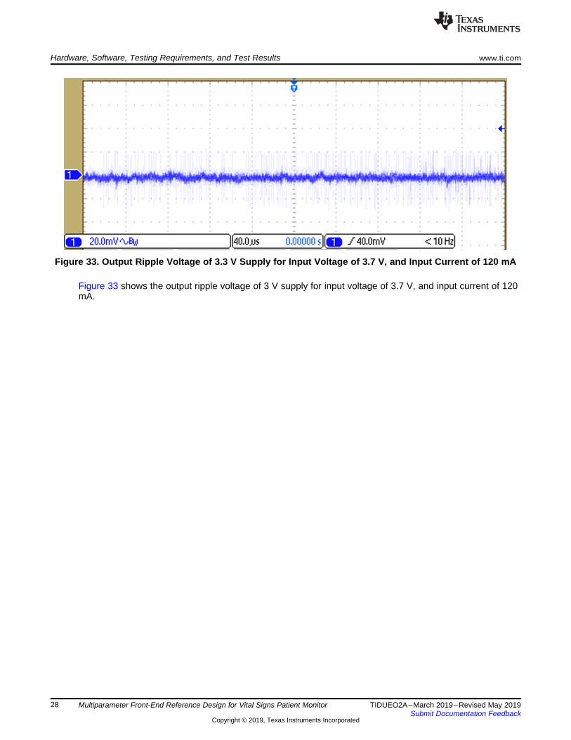
Figure 33. Output Ripple Voltage of 3.3 V Supply for Input Voltage of 3.7 V, and Input Current of 120 mA
Figure 33 shows the output ripple voltage of 3 V supply for input voltage of 3.7 V, and input current of 120mA.

www.ti.com Design Files
29TIDUEO2A–March 2019–Revised May 2019Submit Documentation Feedback
Copyright © 2019, Texas Instruments Incorporated
Multiparameter Front-End Reference Design for Vital Signs Patient Monitor
5 Design Files
5.1 SchematicsSee the design files at TIDA-01614 to download the schematics.
5.2 Bill of MaterialsSee the design files at TIDA-01614 to download the bill of materials (BOM).
5.3 PCB Layout Recommendations
5.3.1 Layout PrintsSee the design files at TIDA-01614 to download the layer plots.
5.4 Altium ProjectSee the design files at TIDA-01614 to download the Altium Designer® project files.
5.5 Gerber FilesSee the design files at TIDA-01614 to download the Gerber files.
5.6 Assembly DrawingsSee the design files at TIDA-01614 to download the assembly drawings.
6 Software FilesSee the design files at TIDA-01614 to download the software files.
7 Related Documentation1. Texas Instruments, Minaturized pulse oximeter reference design getting started guide2. Texas Instruments, How to design peripheral oxygen saturation (SpO2) and optical heart rate
monitoring (OHRM) systems using the AFE4403 application report3. Texas Instruments, Understanding lead-off detection in ECG application report
7.1 TrademarksE2E, Code Composer Studio are trademarks of Texas Instruments.Altium Designer is a registered trademark of Altium LLC or its affiliated companies.SimpleLink is a trademark of other.All other trademarks are the property of their respective owners.
7.2 Third-Party Products DisclaimerTI'S PUBLICATION OF INFORMATION REGARDING THIRD-PARTY PRODUCTS OR SERVICES DOESNOT CONSTITUTE AN ENDORSEMENT REGARDING THE SUITABILITY OF SUCH PRODUCTS ORSERVICES OR A WARRANTY, REPRESENTATION OR ENDORSEMENT OF SUCH PRODUCTS ORSERVICES, EITHER ALONE OR IN COMBINATION WITH ANY TI PRODUCT OR SERVICE.

About the Author www.ti.com
30 TIDUEO2A–March 2019–Revised May 2019Submit Documentation Feedback
Copyright © 2019, Texas Instruments Incorporated
Multiparameter Front-End Reference Design for Vital Signs Patient Monitor
8 About the AuthorLENI SKARIAH is a systems engineer at Texas Instruments, where she is responsible for developingsubsystem design solutions for the Medical, Healthcare, and Fitness sector. Leni brings her experience inprecision analog and mixed signal designs to this role. Leni earned her Bachelor of Technology inElectronics and Communication Engineering from the University of Kannur and her Master of Technologyin Digital Electronics and Communication Systems from Visvesvaraya Technological University,Karnataka.
SANJAY DIXIT is a system architect in the Industrial Systems-Medical Healthcare and Fitness Sector atTexas Instruments where he is responsible for specifying reference designs.
KIRAN RAJMOHAN is a test engineer at Texas Instruments, where he is responsible for testing andcharacterization of high-performance analog IPs like ADC, DAC, PGA, PLL, and RF-signal chains in TImicrocontrollers. Kiran has been with TI since 2015. Kiran earned his Bachelor of Technology inElectronics and Communication Engineering at the College of Engineering, Trivandrum, Kerala.

www.ti.com Revision History
31TIDUEO2A–March 2019–Revised May 2019Submit Documentation Feedback
Copyright © 2019, Texas Instruments Incorporated
Revision History
Revision HistoryNOTE: Page numbers for previous revisions may differ from page numbers in the current version.
Changes from Original (March 2019) to A Revision ....................................................................................................... Page
• Changed TIDA-01614 Block Diagram image in System Overview and on first page ............................................ 5

IMPORTANT NOTICE AND DISCLAIMER
TI PROVIDES TECHNICAL AND RELIABILITY DATA (INCLUDING DATASHEETS), DESIGN RESOURCES (INCLUDING REFERENCEDESIGNS), APPLICATION OR OTHER DESIGN ADVICE, WEB TOOLS, SAFETY INFORMATION, AND OTHER RESOURCES “AS IS”AND WITH ALL FAULTS, AND DISCLAIMS ALL WARRANTIES, EXPRESS AND IMPLIED, INCLUDING WITHOUT LIMITATION ANYIMPLIED WARRANTIES OF MERCHANTABILITY, FITNESS FOR A PARTICULAR PURPOSE OR NON-INFRINGEMENT OF THIRDPARTY INTELLECTUAL PROPERTY RIGHTS.These resources are intended for skilled developers designing with TI products. You are solely responsible for (1) selecting the appropriateTI products for your application, (2) designing, validating and testing your application, and (3) ensuring your application meets applicablestandards, and any other safety, security, or other requirements. These resources are subject to change without notice. TI grants youpermission to use these resources only for development of an application that uses the TI products described in the resource. Otherreproduction and display of these resources is prohibited. No license is granted to any other TI intellectual property right or to any thirdparty intellectual property right. TI disclaims responsibility for, and you will fully indemnify TI and its representatives against, any claims,damages, costs, losses, and liabilities arising out of your use of these resources.TI’s products are provided subject to TI’s Terms of Sale (www.ti.com/legal/termsofsale.html) or other applicable terms available either onti.com or provided in conjunction with such TI products. TI’s provision of these resources does not expand or otherwise alter TI’s applicablewarranties or warranty disclaimers for TI products.
Mailing Address: Texas Instruments, Post Office Box 655303, Dallas, Texas 75265Copyright © 2019, Texas Instruments Incorporated