LM101A/LM201A/LM301A Operational Amplifiers - TI. · PDF fileapplication. For example, in low...
24
LM101A-N, LM201A-N, LM301A-N www.ti.com SNOSBS0D – SEPTEMBER 1999 – REVISED MARCH 2013 LM101A/LM201A/LM301A Operational Amplifiers Check for Samples: LM101A-N, LM201A-N, LM301A-N 1FEATURES DESCRIPTION The LM101A series are general purpose operational • Improved Specifications include: amplifiers which feature improved performance over • Offset Voltage 3 mV Maximum Over industry standards like the LM709. Advanced Temperature (LM101A/LM201A) processing techniques make possible an order of • Input Current 100 nA Maximum Over magnitude reduction in input currents, and a redesign of the biasing circuitry reduces the temperature drift Temperature (LM101A/LM201A) of input current. • Offset Current 20 nA Maximum Over Temperature (LM101A/LM201A) This amplifier offers many features which make its application nearly foolproof: Overload protection on • Specified Drift Characteristics the input and output, no latch-up when the common • Offsets Specified Over Entire Common Mode mode range is exceeded, and freedom from and Supply Voltage Ranges oscillations and compensation with a single 30 pF • Slew Rate of 10V/μs as a Summing Amplifier Capacitor. It has advantages over internally compensated amplifiers in that the frequency compensation can be tailored to the particular application. For example, in low frequency circuits it can be overcompensated for increased stability margin or the compensation can be optimized to give more than a factor of ten improvement in high frequency performance for most applications. In Addition, the device provides better accuracy and lower noise in high impedance circuitry. The low input currents also make it particularly well suited for long interval integrators or timers, sample and hold circuits and low frequency waveform generators. Further, replacing circuits where matched transistor pairs buffer the inputs of conventional IC op amps, It can give lower offset voltage and a drift at a lower cost. The LM101A is ensured over a temperature range of −55°C to +125°C, the LM201A from −25°C to +85°C, and the LM301A from 0°C to +70°C. Fast AC-DC Converter Feedforward compensation can be used to make a fast full wave rectifier without a filter. 1 Please be aware that an important notice concerning availability, standard warranty, and use in critical applications of Texas Instruments semiconductor products and disclaimers thereto appears at the end of this data sheet. PRODUCTION DATA information is current as of publication date. Copyright © 1999–2013, Texas Instruments Incorporated Products conform to specifications per the terms of the Texas Instruments standard warranty. Production processing does not necessarily include testing of all parameters.
Transcript of LM101A/LM201A/LM301A Operational Amplifiers - TI. · PDF fileapplication. For example, in low...
LM101A-N, LM201A-N, LM301A-N
www.ti.com SNOSBS0D –SEPTEMBER 1999–REVISED MARCH 2013
LM101A/LM201A/LM301A Operational AmplifiersCheck for Samples: LM101A-N, LM201A-N, LM301A-N
1FEATURES DESCRIPTIONThe LM101A series are general purpose operational• Improved Specifications include:amplifiers which feature improved performance over
• Offset Voltage 3 mV Maximum Over industry standards like the LM709. AdvancedTemperature (LM101A/LM201A) processing techniques make possible an order of
• Input Current 100 nA Maximum Over magnitude reduction in input currents, and a redesignof the biasing circuitry reduces the temperature driftTemperature (LM101A/LM201A)of input current.• Offset Current 20 nA Maximum Over
Temperature (LM101A/LM201A) This amplifier offers many features which make itsapplication nearly foolproof: Overload protection on• Specified Drift Characteristicsthe input and output, no latch-up when the common• Offsets Specified Over Entire Common Mode mode range is exceeded, and freedom from
and Supply Voltage Ranges oscillations and compensation with a single 30 pF• Slew Rate of 10V/μs as a Summing Amplifier Capacitor. It has advantages over internally
compensated amplifiers in that the frequencycompensation can be tailored to the particularapplication. For example, in low frequency circuits itcan be overcompensated for increased stabilitymargin or the compensation can be optimized to givemore than a factor of ten improvement in highfrequency performance for most applications.
In Addition, the device provides better accuracy andlower noise in high impedance circuitry. The low inputcurrents also make it particularly well suited for longinterval integrators or timers, sample and hold circuitsand low frequency waveform generators. Further,replacing circuits where matched transistor pairsbuffer the inputs of conventional IC op amps, It cangive lower offset voltage and a drift at a lower cost.
The LM101A is ensured over a temperature range of−55°C to +125°C, the LM201A from −25°C to +85°C,and the LM301A from 0°C to +70°C.
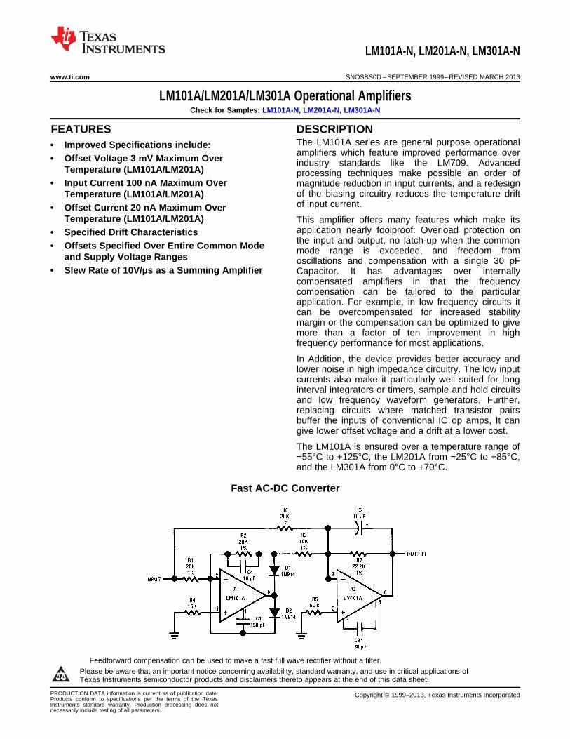
Fast AC-DC Converter
Feedforward compensation can be used to make a fast full wave rectifier without a filter.1
Please be aware that an important notice concerning availability, standard warranty, and use in critical applications ofTexas Instruments semiconductor products and disclaimers thereto appears at the end of this data sheet.
PRODUCTION DATA information is current as of publication date. Copyright © 1999–2013, Texas Instruments IncorporatedProducts conform to specifications per the terms of the TexasInstruments standard warranty. Production processing does notnecessarily include testing of all parameters.
LM101A-N, LM201A-N, LM301A-N
SNOSBS0D –SEPTEMBER 1999–REVISED MARCH 2013 www.ti.com
These devices have limited built-in ESD protection. The leads should be shorted together or the device placed in conductive foamduring storage or handling to prevent electrostatic damage to the MOS gates.
Absolute Maximum Ratings (1) (2)
LM101A/LM201A LM301A
Supply Voltage ±22V ±18V
Differential Input Voltage ±30V ±30V
Input Voltage (3) ±15V ±15V
Output Short Circuit Duration (4) Continuous Continuous
Operating Ambient Temp. Range −55°C to +125°C (LM101A) 0°C to +70°C
−25°C to +85°C (LM201A)
TJ Max
LMC0008C Package 150°C 100°C
P0008E Package 150°C 100°C
NAB0008A, J0014A Package 150°C 100°C
Power Dissipation at TA = 25°C
LMC0008C-Package (Still Air) 500 mW 300 mW
(400 LF/Min Air Flow) 1200 mW 700 mW
P0008E Package 900 mW 500 mW
NAB0008A, J0014A Package 1000 mW 650 mW
Thermal Resistance (Typical) θjA
LMC0008C Package (Still Air) 165°C/W 165°C/W
(400 LF/Min Air Flow) 67°C/W 67°C/W
P0008E Package 135°C/W 135°C/W
NAB0008A, J0014A Package 110°C/W 110°CmW
(Typical) θjC
LMC0008C Package 25°C/W 25°C/W
Storage Temperature Range −65°C to +150°C −65°C to +150°C
Lead Temperature (Soldering, 10 sec.)
LMC0008C or NAB0008A, J0014A, NAD0010A 300°C 300°C
P0008E 260°C 260°C
ESD Tolerance (5) 2000V 2000V
(1) Absolute Maximum Ratings indicate limits beyond which damage to the device may occur. Operating ratings indicate for which thedevice is functional, but do no ensure specific performance limits. Electrical Characteristics state DC and AC electrical specificationsunder particular test conditions which ensure specific limits. This assumes that the device is within the Operating Ratings. Specificationsare not ensured for parameters where no limit is given, however, the typical value is a good indication of device performance.
(2) If Military/Aerospace specified devices are required, please contact the Texas Instruments Sales Office/Distributors for availability andspecifications.
(3) For supply voltages less than ±15V, the absolute maximum input voltage is equal to the supply voltage.(4) Continuous short circuit is allowed for case temperatures to 125°C and ambient temperatures to 75°C for LM101A/LM201A, and 70°C
and 55°C respectively for LM301A.(5) Human body model, 100 pF discharged through 1.5 kΩ.
2 Submit Documentation Feedback Copyright © 1999–2013, Texas Instruments Incorporated
Product Folder Links: LM101A-N LM201A-N LM301A-N

LM101A-N, LM201A-N, LM301A-N
www.ti.com SNOSBS0D –SEPTEMBER 1999–REVISED MARCH 2013
Electrical Characteristics (1)
TA= TJ
LM101A/LM201A LM301AParameter Test Conditions Units
Min Typ Max Min Typ Max
Input Offset Voltage TA = 25°C, RS ≤ 50 kΩ 0.7 2.0 2.0 7.5 mV
Input Offset Current TA = 25°C 1.5 10 3.0 50 nA
Input Bias Current TA = 25°C 30 75 70 250 nA
Input Resistance TA = 25°C 1.5 4.0 0.5 2.0 MΩSupply Current TA = 25°C VS = ±20V 1.8 3.0 mA
VS = ±15V 1.8 3.0 mA
Large Signal Voltage Gain TA = 25°C, VS = ±15V 50 160 25 160 V/mV
VOUT = ±10V, RL ≥ 2 kΩInput Offset Voltage RS ≤ 50 kΩ 3.0 10 mV
Average Temperature Coefficient of RS ≤ 50 kΩ 3.0 15 6.0 30 μV/°CInput Offset Voltage
Input Offset Current 20 70 nA
Average Temperature Coefficient of 25°C ≤ TA ≤ TMAX 0.01 0.1 0.01 0.3 nA/°CInput Offset Current TMIN ≤ TA ≤ 25°C 0.02 0.2 0.02 0.6 nA/°C
Input Bias Current 0.1 0.3 μA
Supply Current TA = TMAX, VS = ±20V 1.2 2.5 mA
Large Signal Voltage Gain VS = ±15V, VOUT = ±10V25 15 V/mV
RL ≥ 2k
Output Voltage Swing VS = ±15V RL = 10 kΩ ±12 ±14 ±12 ±14 V
RL = 2 kΩ ±10 ±13 ±10 ±13 V
Input Voltage Range VS = ±20V ±15 V
VS = ±15V +15, −13 ±12 +15, −13 V
Common-Mode Rejection Ratio RS ≤ 50 kΩ 80 96 70 90 dB
Supply Voltage Rejection Ratio RS ≤ 50 kΩ 80 96 70 96 dB
(1) Unless otherwise specified, these specifications apply for C1 = 30 pF, ±5V ≤ VS ≤ ±20V and −55°C ≤ TA ≤ +125°C (LM101A), ±5V ≤ VS≤ ±20V and −25°C ≤ TA ≤ +85°C (LM201A), ±5V ≤ VS ≤ ±15V and 0°C ≤ TA ≤ +70°C (LM301A).
Copyright © 1999–2013, Texas Instruments Incorporated Submit Documentation Feedback 3
Product Folder Links: LM101A-N LM201A-N LM301A-N

LM101A-N, LM201A-N, LM301A-N
SNOSBS0D –SEPTEMBER 1999–REVISED MARCH 2013 www.ti.com
Typical Performance CharacteristicsLM101A/LM201A
Input Voltage Range Output Swing
Figure 1. Figure 2.
Voltage Gain
Figure 3.
Performance CharacteristicsLM301A
Input Voltage Range Output Swing
Figure 4. Figure 5.
4 Submit Documentation Feedback Copyright © 1999–2013, Texas Instruments Incorporated
Product Folder Links: LM101A-N LM201A-N LM301A-N
LM101A-N, LM201A-N, LM301A-N
www.ti.com SNOSBS0D –SEPTEMBER 1999–REVISED MARCH 2013
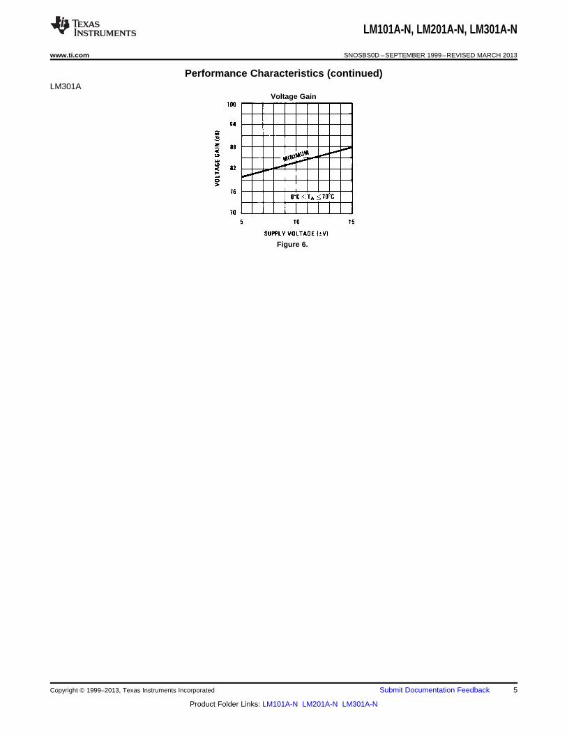
Performance Characteristics (continued)LM301A
Voltage Gain
Figure 6.
Copyright © 1999–2013, Texas Instruments Incorporated Submit Documentation Feedback 5
Product Folder Links: LM101A-N LM201A-N LM301A-N

LM101A-N, LM201A-N, LM301A-N
SNOSBS0D –SEPTEMBER 1999–REVISED MARCH 2013 www.ti.com
Typical Performance Characteristics
Supply Current Voltage Gain
Figure 7. Figure 8.
Input Current,Maximum Power Dissipation LM101A/LM201A/LM301A
Figure 9. Figure 10.
Current Limiting Input Noise Voltage
Figure 11. Figure 12.
6 Submit Documentation Feedback Copyright © 1999–2013, Texas Instruments Incorporated
Product Folder Links: LM101A-N LM201A-N LM301A-N
LM101A-N, LM201A-N, LM301A-N
www.ti.com SNOSBS0D –SEPTEMBER 1999–REVISED MARCH 2013
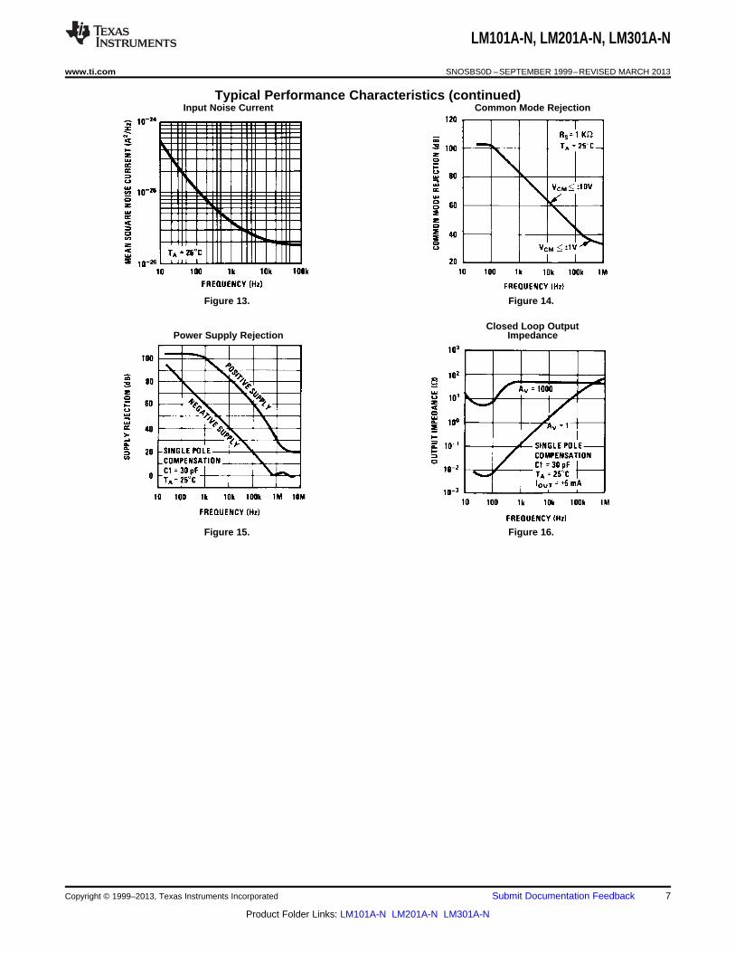
Typical Performance Characteristics (continued)Input Noise Current Common Mode Rejection
Figure 13. Figure 14.
Closed Loop OutputPower Supply Rejection Impedance
Figure 15. Figure 16.
Copyright © 1999–2013, Texas Instruments Incorporated Submit Documentation Feedback 7
Product Folder Links: LM101A-N LM201A-N LM301A-N
LM101A-N, LM201A-N, LM301A-N
SNOSBS0D –SEPTEMBER 1999–REVISED MARCH 2013 www.ti.com
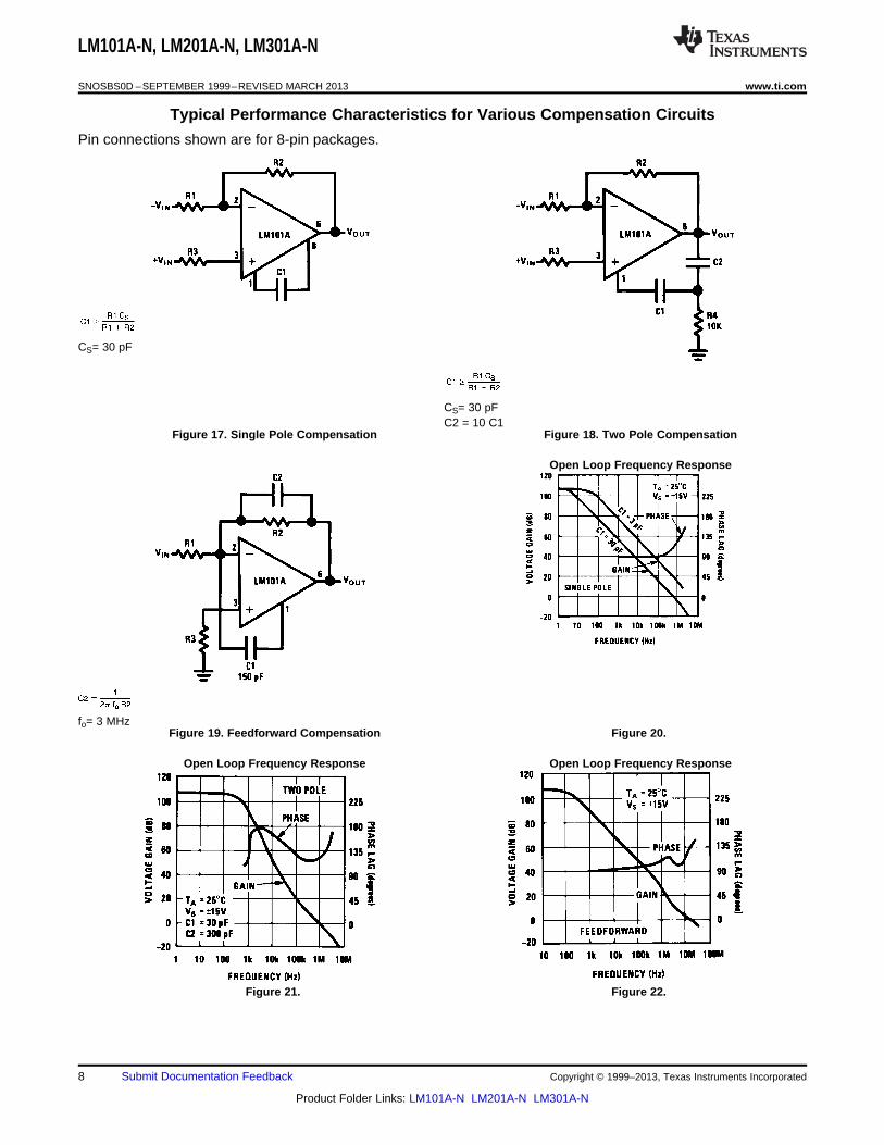
Typical Performance Characteristics for Various Compensation Circuits
Pin connections shown are for 8-pin packages.
CS= 30 pF
CS= 30 pFC2 = 10 C1
Figure 17. Single Pole Compensation Figure 18. Two Pole Compensation
Open Loop Frequency Response
fo= 3 MHzFigure 19. Feedforward Compensation Figure 20.
Open Loop Frequency Response Open Loop Frequency Response
Figure 21. Figure 22.
8 Submit Documentation Feedback Copyright © 1999–2013, Texas Instruments Incorporated
Product Folder Links: LM101A-N LM201A-N LM301A-N

LM101A-N, LM201A-N, LM301A-N
www.ti.com SNOSBS0D –SEPTEMBER 1999–REVISED MARCH 2013
Typical Performance Characteristics for Various Compensation Circuits (continued)Large Signal Frequency Response Large Signal Frequency Response
Figure 23. Figure 24.
Large Signal Frequency Response Voltage Follower Pulse Response
Figure 25. Figure 26.
Voltage Follower Pulse Response Inverter Pulse Response
Figure 27. Figure 28.
Copyright © 1999–2013, Texas Instruments Incorporated Submit Documentation Feedback 9
Product Folder Links: LM101A-N LM201A-N LM301A-N

LM101A-N, LM201A-N, LM301A-N
SNOSBS0D –SEPTEMBER 1999–REVISED MARCH 2013 www.ti.com
TYPICAL APPLICATIONS
Pin connections shown are for 8-pin packages
L ≃ R1 R2 C1RS = R2RP = R1
Figure 29. Variable Capacitance Multiplier Figure 30. Simulated Inductor
Figure 31. Fast Inverting Amplifier with HighInput Impedance
fo = 10 kHz
Figure 33. Sine Wave Oscillator
†May be zero or equal to parallelcombination of R1 and R2 for minimumoffset.
*Adjust for zero integrator drift. Current driftFigure 32. Inverting Amplifier with Balancingtypically 0.1 nA/°C over −55°C to +125°CCircuittemperature range.
Figure 34. Integrator with Bias CurrentCompensation
10 Submit Documentation Feedback Copyright © 1999–2013, Texas Instruments Incorporated
Product Folder Links: LM101A-N LM201A-N LM301A-N
LM101A-N, LM201A-N, LM301A-N
www.ti.com SNOSBS0D –SEPTEMBER 1999–REVISED MARCH 2013
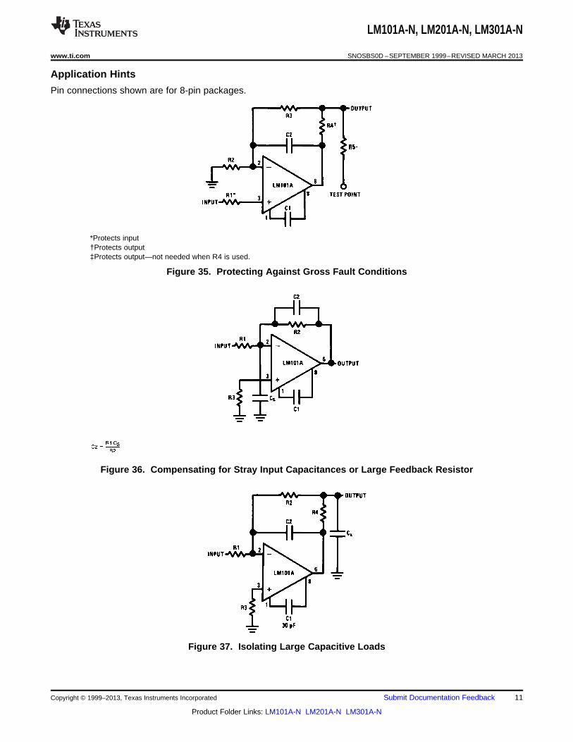
Application Hints
Pin connections shown are for 8-pin packages.
*Protects input†Protects output‡Protects output—not needed when R4 is used.
Figure 35. Protecting Against Gross Fault Conditions
Figure 36. Compensating for Stray Input Capacitances or Large Feedback Resistor
Figure 37. Isolating Large Capacitive Loads
Copyright © 1999–2013, Texas Instruments Incorporated Submit Documentation Feedback 11
Product Folder Links: LM101A-N LM201A-N LM301A-N
LM101A-N, LM201A-N, LM301A-N
SNOSBS0D –SEPTEMBER 1999–REVISED MARCH 2013 www.ti.com
Although the LM101A is designed for trouble free operation, experience has indicated that it is wise to observecertain precautions given below to protect the devices from abnormal operating conditions. It might be pointedout that the advice given here is applicable to practically any IC op amp, although the exact reason why maydiffer with different devices.
When driving either input from a low-impedance source, a limiting resistor should be placed in series with theinput lead to limit the peak instantaneous output current of the source to something less than 100 mA. This isespecially important when the inputs go outside a piece of equipment where they could accidentally beconnected to high voltage sources. Large capacitors on the input (greater than 0.1 μF) should be treated as alow source impedance and isolated with a resistor. Low impedance sources do not cause a problem unless theiroutput voltage exceeds the supply voltage. However, the supplies go to zero when they are turned off, so theisolation is usually needed.
The output circuitry is protected against damage from shorts to ground. However, when the amplifier output isconnected to a test point, it should be isolated by a limiting resistor, as test points frequently get shorted to badplaces. Further, when the amplifer drives a load external to the equipment, it is also advisable to use some sortof limiting resistance to preclude mishaps.
Precautions should be taken to insure that the power supplies for the integrated circuit never becomereversed—even under transient conditions. With reverse voltages greater than 1V, the IC will conduct excessivecurrent, fusing internal aluminum interconnects. If there is a possibility of this happening, clamp diodes with ahigh peak current rating should be installed on the supply lines. Reversal of the voltage between V+ and V− willalways cause a problem, although reversals with respect to ground may also give difficulties in many circuits.
The minimum values given for the frequency compensation capacitor are stable only for source resistances lessthan 10 kΩ, stray capacitances on the summing junction less than 5 pF and capacitive loads smaller than 100pF. If any of these conditions are not met, it becomes necessary to overcompensate the amplifier with a largercompensation capacitor. Alternately, lead capacitors can be used in the feedback network to negate the effect ofstray capacitance and large feedback resistors or an RC network can be added to isolate capacitive loads.
Although the LM101A is relatively unaffected by supply bypassing, this cannot be ignored altogether. Generally itis necessary to bypass the supplies to ground at least once on every circuit card, and more bypass points maybe required if more than five amplifiers are used. When feed-forward compensation is employed, however, it isadvisable to bypass the supply leads of each amplifier with low inductance capacitors because of the higherfrequencies involved.
12 Submit Documentation Feedback Copyright © 1999–2013, Texas Instruments Incorporated
Product Folder Links: LM101A-N LM201A-N LM301A-N

LM101A-N, LM201A-N, LM301A-N
www.ti.com SNOSBS0D –SEPTEMBER 1999–REVISED MARCH 2013
Typical Applications
Pin connections shown are for 8-pin packages.
Figure 38. Standard Compensation and Offset Balancing Circuit
Power Bandwidth: 15 kHzSlew Rate: 1V/μs
Figure 39. Fast Voltage Follower
Power Bandwidth: 250 kHzSmall Signal Bandwiidth: 3.5 MHzSlew Rate: 10V/μs
Figure 40. Fast Summing Amplifier
Copyright © 1999–2013, Texas Instruments Incorporated Submit Documentation Feedback 13
Product Folder Links: LM101A-N LM201A-N LM301A-N

LM101A-N, LM201A-N, LM301A-N
SNOSBS0D –SEPTEMBER 1999–REVISED MARCH 2013 www.ti.com
R3 = R4 + R5R1 = R2
Figure 41. Bilateral Current Source
Figure 42. Fast AC/DC Converter (1)
R1 = R4; R2 = R3
*,† Matching determines CMRR.
Figure 43. Instrumentation Amplifier
(1) Feedforward compensation can be used to make a fast full wave rectifier without a filter
14 Submit Documentation Feedback Copyright © 1999–2013, Texas Instruments Incorporated
Product Folder Links: LM101A-N LM201A-N LM301A-N

LM101A-N, LM201A-N, LM301A-N
www.ti.com SNOSBS0D –SEPTEMBER 1999–REVISED MARCH 2013
*Adjust for zero integrator drift. Current drift typically 0.1 nA/°C over 0°C to +70°C temperature range.
Figure 44. Integrator with Bias Current Compensation
Figure 45. Voltage Comparator for Driving RTL Logic or High Current Driver
Figure 46. Low Frequency Square Wave Generator
*Polycarbonate-dielectric capacitor
Figure 47. Low Drift Sample and Hold
Copyright © 1999–2013, Texas Instruments Incorporated Submit Documentation Feedback 15
Product Folder Links: LM101A-N LM201A-N LM301A-N

LM101A-N, LM201A-N, LM301A-N
SNOSBS0D –SEPTEMBER 1999–REVISED MARCH 2013 www.ti.com
Figure 48. Voltage Comparator for Driving DTL or TTL Integrated Circuits
Schematic
Pin connections shown are for 8-pin packages.
16 Submit Documentation Feedback Copyright © 1999–2013, Texas Instruments Incorporated
Product Folder Links: LM101A-N LM201A-N LM301A-N

LM101A-N, LM201A-N, LM301A-N
www.ti.com SNOSBS0D –SEPTEMBER 1999–REVISED MARCH 2013
Connection Diagrams
Top ViewTop View
Figure 49. CDIP and PDIP PackagesPackage Number NAB0008A or P0008E
Top View Figure 51. TO-99 PackageSee Package Number LMC0008C
Top View
Figure 50. CLGA PackagePackage Number NAD0010A
Figure 52. CDIP PackageSee Package Number J0014A,
Copyright © 1999–2013, Texas Instruments Incorporated Submit Documentation Feedback 17
Product Folder Links: LM101A-N LM201A-N LM301A-N
LM101A-N, LM201A-N, LM301A-N
SNOSBS0D –SEPTEMBER 1999–REVISED MARCH 2013 www.ti.com
REVISION HISTORY
Changes from Revision C (March 2013) to Revision D Page
• Changed layout of National Data Sheet to TI format .......................................................................................................... 17
18 Submit Documentation Feedback Copyright © 1999–2013, Texas Instruments Incorporated
Product Folder Links: LM101A-N LM201A-N LM301A-N
PACKAGE OPTION ADDENDUM
www.ti.com 14-Aug-2017
Addendum-Page 1
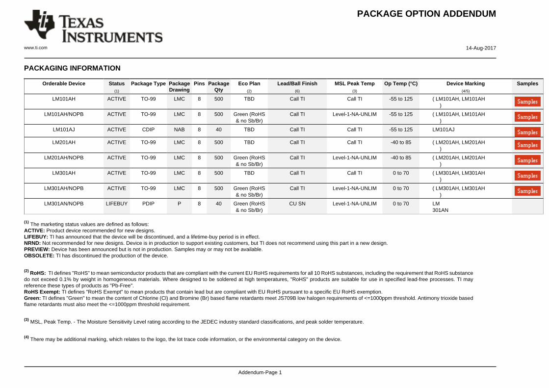
PACKAGING INFORMATION
Orderable Device Status(1)
Package Type PackageDrawing
Pins PackageQty
Eco Plan(2)
Lead/Ball Finish(6)
MSL Peak Temp(3)
Op Temp (°C) Device Marking(4/5)
Samples
LM101AH ACTIVE TO-99 LMC 8 500 TBD Call TI Call TI -55 to 125 ( LM101AH, LM101AH )
LM101AH/NOPB ACTIVE TO-99 LMC 8 500 Green (RoHS& no Sb/Br)
Call TI Level-1-NA-UNLIM -55 to 125 ( LM101AH, LM101AH )
LM101AJ ACTIVE CDIP NAB 8 40 TBD Call TI Call TI -55 to 125 LM101AJ
LM201AH ACTIVE TO-99 LMC 8 500 TBD Call TI Call TI -40 to 85 ( LM201AH, LM201AH )
LM201AH/NOPB ACTIVE TO-99 LMC 8 500 Green (RoHS& no Sb/Br)
Call TI Level-1-NA-UNLIM -40 to 85 ( LM201AH, LM201AH )
LM301AH ACTIVE TO-99 LMC 8 500 TBD Call TI Call TI 0 to 70 ( LM301AH, LM301AH )
LM301AH/NOPB ACTIVE TO-99 LMC 8 500 Green (RoHS& no Sb/Br)
Call TI Level-1-NA-UNLIM 0 to 70 ( LM301AH, LM301AH )
LM301AN/NOPB LIFEBUY PDIP P 8 40 Green (RoHS& no Sb/Br)
CU SN Level-1-NA-UNLIM 0 to 70 LM301AN
(1) The marketing status values are defined as follows:ACTIVE: Product device recommended for new designs.LIFEBUY: TI has announced that the device will be discontinued, and a lifetime-buy period is in effect.NRND: Not recommended for new designs. Device is in production to support existing customers, but TI does not recommend using this part in a new design.PREVIEW: Device has been announced but is not in production. Samples may or may not be available.OBSOLETE: TI has discontinued the production of the device.
(2) RoHS: TI defines "RoHS" to mean semiconductor products that are compliant with the current EU RoHS requirements for all 10 RoHS substances, including the requirement that RoHS substancedo not exceed 0.1% by weight in homogeneous materials. Where designed to be soldered at high temperatures, "RoHS" products are suitable for use in specified lead-free processes. TI mayreference these types of products as "Pb-Free".RoHS Exempt: TI defines "RoHS Exempt" to mean products that contain lead but are compliant with EU RoHS pursuant to a specific EU RoHS exemption.Green: TI defines "Green" to mean the content of Chlorine (Cl) and Bromine (Br) based flame retardants meet JS709B low halogen requirements of <=1000ppm threshold. Antimony trioxide basedflame retardants must also meet the <=1000ppm threshold requirement.
(3) MSL, Peak Temp. - The Moisture Sensitivity Level rating according to the JEDEC industry standard classifications, and peak solder temperature.
(4) There may be additional marking, which relates to the logo, the lot trace code information, or the environmental category on the device.
PACKAGE OPTION ADDENDUM
www.ti.com 14-Aug-2017
Addendum-Page 2
(5) Multiple Device Markings will be inside parentheses. Only one Device Marking contained in parentheses and separated by a "~" will appear on a device. If a line is indented then it is a continuationof the previous line and the two combined represent the entire Device Marking for that device.
(6) Lead/Ball Finish - Orderable Devices may have multiple material finish options. Finish options are separated by a vertical ruled line. Lead/Ball Finish values may wrap to two lines if the finishvalue exceeds the maximum column width.
Important Information and Disclaimer:The information provided on this page represents TI's knowledge and belief as of the date that it is provided. TI bases its knowledge and belief on informationprovided by third parties, and makes no representation or warranty as to the accuracy of such information. Efforts are underway to better integrate information from third parties. TI has taken andcontinues to take reasonable steps to provide representative and accurate information but may not have conducted destructive testing or chemical analysis on incoming materials and chemicals.TI and TI suppliers consider certain information to be proprietary, and thus CAS numbers and other limited information may not be available for release.
In no event shall TI's liability arising out of such information exceed the total purchase price of the TI part(s) at issue in this document sold by TI to Customer on an annual basis.
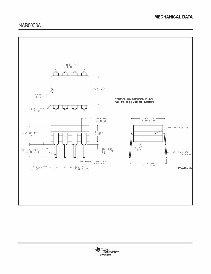
MECHANICAL DATA
NAB0008A
www.ti.com
J08A (Rev M)


IMPORTANT NOTICE
Texas Instruments Incorporated (TI) reserves the right to make corrections, enhancements, improvements and other changes to itssemiconductor products and services per JESD46, latest issue, and to discontinue any product or service per JESD48, latest issue. Buyersshould obtain the latest relevant information before placing orders and should verify that such information is current and complete.TI’s published terms of sale for semiconductor products (http://www.ti.com/sc/docs/stdterms.htm) apply to the sale of packaged integratedcircuit products that TI has qualified and released to market. Additional terms may apply to the use or sale of other types of TI products andservices.Reproduction of significant portions of TI information in TI data sheets is permissible only if reproduction is without alteration and isaccompanied by all associated warranties, conditions, limitations, and notices. TI is not responsible or liable for such reproduceddocumentation. Information of third parties may be subject to additional restrictions. Resale of TI products or services with statementsdifferent from or beyond the parameters stated by TI for that product or service voids all express and any implied warranties for theassociated TI product or service and is an unfair and deceptive business practice. TI is not responsible or liable for any such statements.Buyers and others who are developing systems that incorporate TI products (collectively, “Designers”) understand and agree that Designersremain responsible for using their independent analysis, evaluation and judgment in designing their applications and that Designers havefull and exclusive responsibility to assure the safety of Designers' applications and compliance of their applications (and of all TI productsused in or for Designers’ applications) with all applicable regulations, laws and other applicable requirements. Designer represents that, withrespect to their applications, Designer has all the necessary expertise to create and implement safeguards that (1) anticipate dangerousconsequences of failures, (2) monitor failures and their consequences, and (3) lessen the likelihood of failures that might cause harm andtake appropriate actions. Designer agrees that prior to using or distributing any applications that include TI products, Designer willthoroughly test such applications and the functionality of such TI products as used in such applications.TI’s provision of technical, application or other design advice, quality characterization, reliability data or other services or information,including, but not limited to, reference designs and materials relating to evaluation modules, (collectively, “TI Resources”) are intended toassist designers who are developing applications that incorporate TI products; by downloading, accessing or using TI Resources in anyway, Designer (individually or, if Designer is acting on behalf of a company, Designer’s company) agrees to use any particular TI Resourcesolely for this purpose and subject to the terms of this Notice.TI’s provision of TI Resources does not expand or otherwise alter TI’s applicable published warranties or warranty disclaimers for TIproducts, and no additional obligations or liabilities arise from TI providing such TI Resources. TI reserves the right to make corrections,enhancements, improvements and other changes to its TI Resources. TI has not conducted any testing other than that specificallydescribed in the published documentation for a particular TI Resource.Designer is authorized to use, copy and modify any individual TI Resource only in connection with the development of applications thatinclude the TI product(s) identified in such TI Resource. NO OTHER LICENSE, EXPRESS OR IMPLIED, BY ESTOPPEL OR OTHERWISETO ANY OTHER TI INTELLECTUAL PROPERTY RIGHT, AND NO LICENSE TO ANY TECHNOLOGY OR INTELLECTUAL PROPERTYRIGHT OF TI OR ANY THIRD PARTY IS GRANTED HEREIN, including but not limited to any patent right, copyright, mask work right, orother intellectual property right relating to any combination, machine, or process in which TI products or services are used. Informationregarding or referencing third-party products or services does not constitute a license to use such products or services, or a warranty orendorsement thereof. Use of TI Resources may require a license from a third party under the patents or other intellectual property of thethird party, or a license from TI under the patents or other intellectual property of TI.TI RESOURCES ARE PROVIDED “AS IS” AND WITH ALL FAULTS. TI DISCLAIMS ALL OTHER WARRANTIES ORREPRESENTATIONS, EXPRESS OR IMPLIED, REGARDING RESOURCES OR USE THEREOF, INCLUDING BUT NOT LIMITED TOACCURACY OR COMPLETENESS, TITLE, ANY EPIDEMIC FAILURE WARRANTY AND ANY IMPLIED WARRANTIES OFMERCHANTABILITY, FITNESS FOR A PARTICULAR PURPOSE, AND NON-INFRINGEMENT OF ANY THIRD PARTY INTELLECTUALPROPERTY RIGHTS. TI SHALL NOT BE LIABLE FOR AND SHALL NOT DEFEND OR INDEMNIFY DESIGNER AGAINST ANY CLAIM,INCLUDING BUT NOT LIMITED TO ANY INFRINGEMENT CLAIM THAT RELATES TO OR IS BASED ON ANY COMBINATION OFPRODUCTS EVEN IF DESCRIBED IN TI RESOURCES OR OTHERWISE. IN NO EVENT SHALL TI BE LIABLE FOR ANY ACTUAL,DIRECT, SPECIAL, COLLATERAL, INDIRECT, PUNITIVE, INCIDENTAL, CONSEQUENTIAL OR EXEMPLARY DAMAGES INCONNECTION WITH OR ARISING OUT OF TI RESOURCES OR USE THEREOF, AND REGARDLESS OF WHETHER TI HAS BEENADVISED OF THE POSSIBILITY OF SUCH DAMAGES.Unless TI has explicitly designated an individual product as meeting the requirements of a particular industry standard (e.g., ISO/TS 16949and ISO 26262), TI is not responsible for any failure to meet such industry standard requirements.Where TI specifically promotes products as facilitating functional safety or as compliant with industry functional safety standards, suchproducts are intended to help enable customers to design and create their own applications that meet applicable functional safety standardsand requirements. Using products in an application does not by itself establish any safety features in the application. Designers mustensure compliance with safety-related requirements and standards applicable to their applications. Designer may not use any TI products inlife-critical medical equipment unless authorized officers of the parties have executed a special contract specifically governing such use.Life-critical medical equipment is medical equipment where failure of such equipment would cause serious bodily injury or death (e.g., lifesupport, pacemakers, defibrillators, heart pumps, neurostimulators, and implantables). Such equipment includes, without limitation, allmedical devices identified by the U.S. Food and Drug Administration as Class III devices and equivalent classifications outside the U.S.TI may expressly designate certain products as completing a particular qualification (e.g., Q100, Military Grade, or Enhanced Product).Designers agree that it has the necessary expertise to select the product with the appropriate qualification designation for their applicationsand that proper product selection is at Designers’ own risk. Designers are solely responsible for compliance with all legal and regulatoryrequirements in connection with such selection.Designer will fully indemnify TI and its representatives against any damages, costs, losses, and/or liabilities arising out of Designer’s non-compliance with the terms and provisions of this Notice.
Mailing Address: Texas Instruments, Post Office Box 655303, Dallas, Texas 75265Copyright © 2017, Texas Instruments Incorporated