Linking an FPGA Project to a PCB Project - Altiumvalhalla.altium.com/Learning-Guides/AP0102 Linking...
38
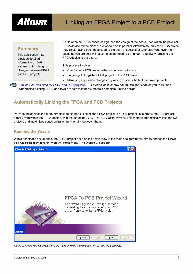
Linking an FPGA Project to a PCB Project Version (v2.1) Sep 09, 2008 1 Quite often an FPGA-based design, and the design of the board upon which the physical FPGA device will be placed, are worked on in parallel. Alternatively, only the FPGA project may exist, having been developed to the point of successful synthesis. Whatever the case, the two projects will, at some stage, need to be linked – effectively targeting the FPGA device to the board. This process involves: • Creation of a PCB project (where one does not exist) • Targeting (linking) the FPGA project to the PCB project • Managing any design changes originating in one or both of the linked projects. How do I link and sync my FPGA and PCB projects? – this video looks at how Altium Designer enables you to link and synchronize existing FPGA and PCB projects together to create a complete, unified design. Automatically Linking the FPGA and PCB Projects Perhaps the easiest and more streamlined method of linking the FPGA project to a PCB project, is to create the PCB project directly from within the FPGA design, with the aid of the FPGA To PCB Project Wizard. This method automatically links the two projects and maximizes synchronization functionality between them. Running the Wizard With a schematic document in the FPGA project open as the active view in the main design window, simply choose the FPGA To PCB Project Wizard entry on the Tools menu. The Wizard will appear. Figure 1. FPGA To PCB Project Wizard – streamlining the linkage of FPGA and PCB projects. Summary This application note provides detailed information on linking and managing design changes between FPGA and PCB projects.
Transcript of Linking an FPGA Project to a PCB Project - Altiumvalhalla.altium.com/Learning-Guides/AP0102 Linking...
Linking an FPGA Project to a PCB Project
Version (v2.1) Sep 09, 2008 1
Quite often an FPGA-based design, and the design of the board upon which the physical FPGA device will be placed, are worked on in parallel. Alternatively, only the FPGA project may exist, having been developed to the point of successful synthesis. Whatever the case, the two projects will, at some stage, need to be linked – effectively targeting the FPGA device to the board.
This process involves:
• Creation of a PCB project (where one does not exist)
• Targeting (linking) the FPGA project to the PCB project
• Managing any design changes originating in one or both of the linked projects.
How do I link and sync my FPGA and PCB projects? – this video looks at how Altium Designer enables you to link and synchronize existing FPGA and PCB projects together to create a complete, unified design.
Automatically Linking the FPGA and PCB Projects
Perhaps the easiest and more streamlined method of linking the FPGA project to a PCB project, is to create the PCB project directly from within the FPGA design, with the aid of the FPGA To PCB Project Wizard. This method automatically links the two projects and maximizes synchronization functionality between them.
Running the Wizard
With a schematic document in the FPGA project open as the active view in the main design window, simply choose the FPGA To PCB Project Wizard entry on the Tools menu. The Wizard will appear.
Figure 1. FPGA To PCB Project Wizard – streamlining the linkage of FPGA and PCB projects.
Summary This application note provides detailed information on linking and managing design changes between FPGA and PCB projects.
AP0102 Linking an FPGA Project to a PCB Project
Version (v2.1) Sep 09, 2008 2
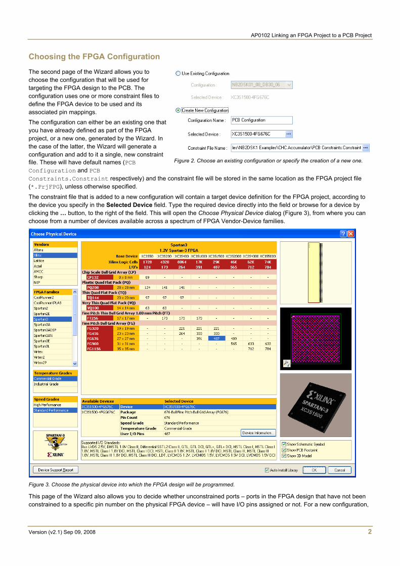
Choosing the FPGA Configuration
The second page of the Wizard allows you to choose the configuration that will be used for targeting the FPGA design to the PCB. The configuration uses one or more constraint files to define the FPGA device to be used and its associated pin mappings.
The configuration can either be an existing one that you have already defined as part of the FPGA project, or a new one, generated by the Wizard. In the case of the latter, the Wizard will generate a configuration and add to it a single, new constraint file. These will have default names (PCB Configuration and PCB Constraints.Constraint respectively) and the constraint file will be stored in the same location as the FPGA project file (*.PrjFPG), unless otherwise specified.
The constraint file that is added to a new configuration will contain a target device definition for the FPGA project, according to the device you specify in the Selected Device field. Type the required device directly into the field or browse for a device by clicking the … button, to the right of the field. This will open the Choose Physical Device dialog (Figure 3), from where you can choose from a number of devices available across a spectrum of FPGA Vendor-Device families.
Figure 3. Choose the physical device into which the FPGA design will be programmed.
This page of the Wizard also allows you to decide whether unconstrained ports – ports in the FPGA design that have not been constrained to a specific pin number on the physical FPGA device – will have I/O pins assigned or not. For a new configuration,
Figure 2. Choose an existing configuration or specify the creation of a new one.
AP0102 Linking an FPGA Project to a PCB Project
Version (v2.1) Sep 09, 2008 3
this will include all ports. However, this will not result in optimal pin allocation and better results can be obtained by importing pin allocations acquired from the vendor place and route tools.
Choosing the Target PCB Project
After choosing the FPGA configuration, the actual target PCB project must now be defined. This is performed on the third page of the Wizard. By default, the Wizard will generate a new project (PCB Project1.PrjPCB), with the project file set to be stored in the same location as the FPGA project. Change the name (and/or path) for the new project as required, either directly in the PCB Project File Name field, or in the Select PCB Project File Name dialog (accessed by clicking on the field's ... button). You can also choose to use an existing PCB project.
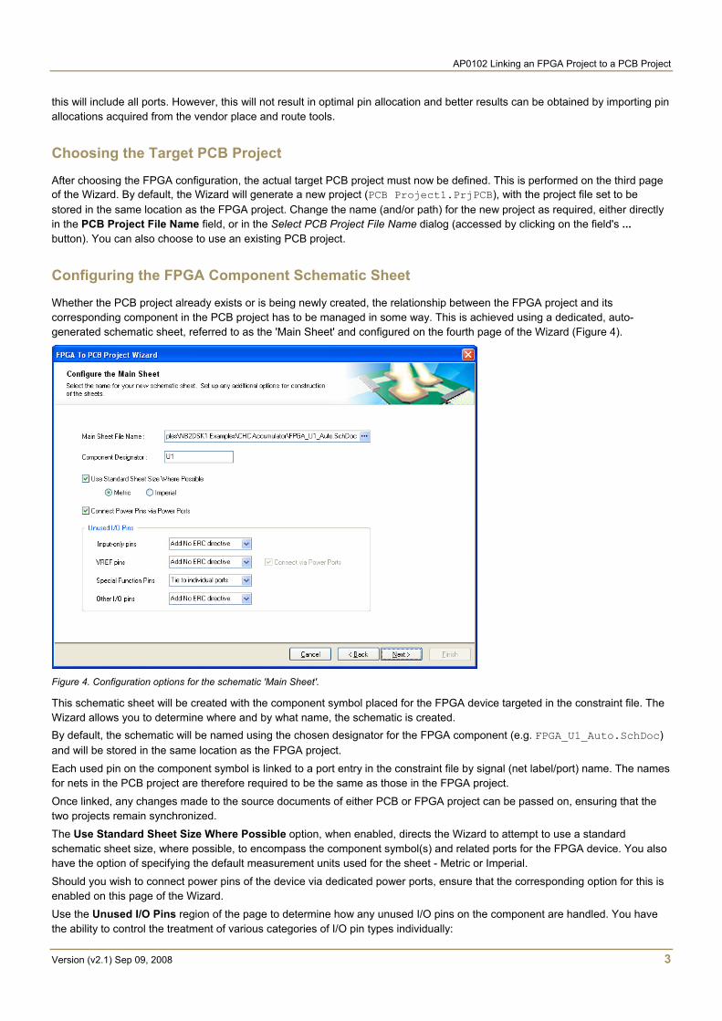
Configuring the FPGA Component Schematic Sheet
Whether the PCB project already exists or is being newly created, the relationship between the FPGA project and its corresponding component in the PCB project has to be managed in some way. This is achieved using a dedicated, auto-generated schematic sheet, referred to as the 'Main Sheet' and configured on the fourth page of the Wizard (Figure 4).
Figure 4. Configuration options for the schematic 'Main Sheet'.
This schematic sheet will be created with the component symbol placed for the FPGA device targeted in the constraint file. The Wizard allows you to determine where and by what name, the schematic is created. By default, the schematic will be named using the chosen designator for the FPGA component (e.g. FPGA_U1_Auto.SchDoc) and will be stored in the same location as the FPGA project.
Each used pin on the component symbol is linked to a port entry in the constraint file by signal (net label/port) name. The names for nets in the PCB project are therefore required to be the same as those in the FPGA project.
Once linked, any changes made to the source documents of either PCB or FPGA project can be passed on, ensuring that the two projects remain synchronized. The Use Standard Sheet Size Where Possible option, when enabled, directs the Wizard to attempt to use a standard schematic sheet size, where possible, to encompass the component symbol(s) and related ports for the FPGA device. You also have the option of specifying the default measurement units used for the sheet - Metric or Imperial.
Should you wish to connect power pins of the device via dedicated power ports, ensure that the corresponding option for this is enabled on this page of the Wizard. Use the Unused I/O Pins region of the page to determine how any unused I/O pins on the component are handled. You have the ability to control the treatment of various categories of I/O pin types individually:
AP0102 Linking an FPGA Project to a PCB Project
Version (v2.1) Sep 09, 2008 4
• Input-only pins
• VREF pins
• Special Function pins and
• all other unused I/O pins.
The pins can be handled in one of the following ways:
Tie to single port - Tie all unused pins in the category to a single port (which will also appear on the parent sheet symbol (if applicable) on the sheet above)
Tie to individual ports - Tie all unused pins in the category to their own, individual ports (which will also appear on the parent sheet symbol (if applicable) on the sheet above)
Tie to ports by IO bank (VREF only)
- Tie all unused VREF pins to a port on a bank by bank basis (which will also appear on the parent sheet symbol (if applicable) on the sheet above).
Add No ERC directive - Add a No ERC directive to an unused pin, so that it is not included as part of error checking when the design is compiled
Ignore - Do nothing with an unused pin
Note: For VREF pins, when the Tie to single port or Tie to ports by IO bank options are selected, you are given the additional option of whether or not to connect via Power Ports.
1
1
2
2
3
3
4
4
5
5
6
6
7
7
8
8
9
9
10
10
11
11
12
12
D D
C C
B B
A A
Title
Number RevisionSize
A1
Date: 27/08/2008 Sheet ofFile: C:\Program Files\..\FPGA_U1_Auto.SchDocDrawn By:
BA
NK
0 IO_L32P_0/GCLK6 A13
IO_L32N_0/GCLK7 B13
IO_L31P_0/VREF_0 C13
IO_L31N_0 D13
IO E13
IO_L30P_0 F13
IO_L30N_0 G13
IO_L29P_0 A12
IO_L29N_0 B12
IO C12
IO_L28P_0 E12
IO_L28N_0 F12
IO_L27P_0 H13
IO_L27N_0 G12
IO H12
IO_L26P_0/VREF_0 A11
IO_L26N_0 B11
IO_L25P_0 D11
IO_L25N_0 E11
IO_L24P_0 F11
IO_L24N_0 G11
IO H11
IO_L23P_0 A10
IO_L23N_0 B10
IO_L22P_0 C10
IO_L22N_0 D10
IO_L19P_0 E10
IO_L19N_0 F10
IO/VREF_0 G10
IO_L18P_0 B9
IO_L18N_0 C9
IO_L17P_0 D9
IO_L17N_0 E9
IO_L16P_0 F9
IO_L16N_0 G9
IO_L15P_0 A8
IO_L15N_0 B8
IO C8
IO_L12P_0 D8
IO_L12N_0 E8
IO_L11P_0 F8
IO_L11N_0 G8
IO_L10P_0 A7
IO_L10N_0 B7
IO_L09P_0 D7
IO_L09N_0 E7
IO/VREF_0 F7
IO A6
IO_L08P_0 B6
IO_L08N_0 C6
IO_L07P_0 D6
IO_L07N_0 E6
IO A5
IO_L06P_0 B5
IO_L06N_0 C5
IO_L05P_0/VREF_0 A4
IO_L05N_0 B4
IO C4
IO A3
IO_L01P_0/VRN_0 D5
IO_L01N_0/VRP_0 E5
IO/VREF_0 B3
U1A
XC3S1500-4FG676C
BA
NK
1 IO A14
IO_L32N_1/GCLK5 B14
IO_L32P_1/GCLK4 C14
IO_L31N_1/VREF_1 D14
IO_L31P_1 E14
IO F14
IO_L30N_1 G14
IO_L30P_1 H14
IO_L29N_1 A15
IO_L29P_1 B15
IO/VREF_1 C15
IO_L28N_1 E15
IO_L28P_1 F15
IO_L27N_1 G15
IO_L27P_1 H15
IO_L26N_1 A16
IO_L26P_1 B16
IO D16
IO_L25N_1 E16
IO_L25P_1 F16
IO_L24N_1 G16
IO_L24P_1 H16
IO_L23N_1 A17
IO_L23P_1 B17
IO/VREF_1 C17
IO_L22N_1 D17
IO_L22P_1 E17
IO_L19N_1 F17
IO_L19P_1 G17
IO_L18N_1 B18
IO_L18P_1 C18
IO/VREF_1 D18
IO E18
IO_L16N_1 F18
IO_L16P_1 G18
IO_L15N_1 A19
IO_L15P_1 B19
IO_L12N_1 C19
IO_L12P_1 D19
IO_L11N_1 E19
IO_L11P_1 F19
IO G19
IO_L10N_1/VREF_1 A20
IO_L10P_1 B20
IO_L09N_1 D20
IO_L09P_1 E20
IO F20
IO_L08N_1 A21
IO_L08P_1 B21
IO_L07N_1 C21
IO_L07P_1 D21
IO_L06N_1/VREF_1 B22
IO_L06P_1 C22
IO_L05N_1 E21
IO_L05P_1 F21
IO A22
IO_L04N_1 B23
IO_L04P_1 C23
IO_L01N_1/VRP_1 D22
IO_L01P_1/VRN_1 E22
IO A23
U1B
XC3S1500-4FG676C
BA
NK
2 IO_L01N_2/VRP_2 C25
IO_L01P_2/VRN_2 C26
IO_L02N_2 E23
IO_L02P_2 E24
IO_L03P_2 D26
IO_L03N_2/VREF_2 D25
IO_L05N_2 E25
IO_L05P_2 E26
IO_L06N_2 G20
IO_L06P_2 G21
IO_L07N_2 F23
IO_L07P_2 F24
IO_L08N_2 G22
IO_L08P_2 G23
IO_L09N_2/VREF_2 F25
IO_L09P_2 F26
IO_L10N_2 G25
IO_L10P_2 G26
IO_L14N_2 H20
IO_L14P_2 H21
IO_L16N_2 H22
IO_L16P_2 J21
IO_L17P_2/VREF_2 H24
IO_L17N_2 H23
IO_L19N_2 H25
IO_L19P_2 H26
IO_L20N_2 J20
IO_L20P_2 K20
IO_L21N_2 J22
IO_L21P_2 J23
IO_L22N_2 J24
IO_L22P_2 J25
IO_L23P_2 K22
IO_L23N_2/VREF_2 K21
IO_L24N_2 K23
IO_L24P_2 K24
IO_L26N_2 K25
IO_L26P_2 K26
IO_L27N_2 L19
IO_L27P_2 L20
IO_L28N_2 L21
IO_L28P_2 L22
IO_L29N_2 L25
IO_L29P_2 L26
IO_L31N_2 M19
IO_L31P_2 M20
IO_L32N_2 M21
IO_L32P_2 M22
IO_L33P_2 M24
IO_L33N_2 L23
IO_L34P_2 M26
IO_L34N_2/VREF_2 M25
IO_L35N_2 N19
IO_L35P_2 N20
IO_L38N_2 N21
IO_L38P_2 N22
IO_L39N_2 N23
IO_L39P_2 N24
IO_L40N_2 N25
IO_L40P_2/VREF_2 N26
U1C
XC3S1500-4FG676C
BA
NK
3 IO_L40N_3/VREF_3 P26
IO_L40P_3 P25
IO_L39N_3 P24
IO_L39P_3 P23
IO_L38N_3 P22
IO_L38P_3 P21
IO_L35N_3 P20
IO_L35P_3 P19
IO_L34N_3 R26
IO_L34P_3/VREF_3 R25
IO_L33N_3 R24
IO_L33P_3 T23
IO_L32N_3 R22
IO_L32P_3 R21
IO_L31N_3 R20
IO_L31P_3 R19
IO_L29N_3 T26
IO_L29P_3 T25
IO_L28N_3 T22
IO_L28P_3 T21
IO_L27N_3 T20
IO_L27P_3 T19
IO_L26N_3 U26
IO_L26P_3 U25
IO_L24N_3 U24
IO_L24P_3 U23
IO_L23N_3 U22
IO_L23P_3/VREF_3 U21
IO_L22N_3 V25
IO_L22P_3 V24
IO_L21N_3 V23
IO_L21P_3 V22
IO_L20N_3 U20
IO_L20P_3 V20
IO_L19N_3 W26
IO_L19P_3 W25
IO_L17N_3 W24
IO_L17P_3/VREF_3 W23
IO_L16N_3 V21
IO_L16P_3 W22
IO_L14N_3 Y26
IO_L14P_3 Y25
IO_L10N_3 W21
IO_L10P_3 W20
IO_L09N_3 AA26
IO_L09P_3/VREF_3 AA25
IO_L08N_3 Y23
IO_L08P_3 Y22
IO_L07N_3 AA24
IO_L07P_3 AA23
IO_L06N_3 AB26
IO_L06P_3 AB25
IO_L05N_3 Y21
IO_L05P_3 Y20
IO_L03N_3 AC26
IO_L03P_3 AC25
IO_L02N_3/VREF_3 AB24
IO_L02P_3 AB23
IO_L01N_3/VRP_3 AA22
IO_L01P_3/VRN_3 AA21
U1D
XC3S1500-4FG676C
BA
NK
4 IO_L32P_4/GCLK0 AF14
IO_L32N_4/GCLK1 AE14
IO_L31P_4/DOUT/BUSY AD14
IO_L31N_4/INIT_B AC14
IO/VREF_4 AB14
IO_L30P_4/D3 AA14
IO_L30N_4/D2 Y14
IO_L29P_4 AF15
IO_L29N_4 AE15
IO AD15
IO_L28P_4 AB15
IO_L28N_4 AA15
IO_L27P_4/D1 W14
IO_L27N_4/DIN/D0 Y15
IO W15
IO_L26P_4/VREF_4 AF16
IO_L26N_4 AE16
IO_L25P_4 AC16
IO_L25N_4 AB16
IO_L24P_4 AA16
IO_L24N_4 Y16
IO W16
IO_L23P_4 AF17
IO_L23N_4 AE17
IO_L22N_4/VREF_4 AD17
IO_L22P_4 AB17
IO_L19N_4 AC17
IO_L19P_4 AA17
IO/VREF_4 Y17
IO_L18P_4 AE18
IO_L18N_4 AD18
IO_L17P_4 AC18
IO_L17N_4 AB18
IO_L16P_4 AA18
IO_L16N_4 Y18
IO_L15P_4 AF19
IO_L15N_4 AE19
IO AD19
IO_L12P_4 AC19
IO_L12N_4 AB19
IO_L11P_4 AA19
IO_L11N_4 Y19
IO_L10P_4 AF20
IO_L10N_4 AE20
IO_L09P_4 AC20
IO_L09N_4 AB20
IO AA20
IO AF21
IO_L08P_4 AE21
IO_L08N_4 AD21
IO_L07P_4 AC21
IO_L07N_4 AB21
IO AF22
IO_L06P_4 AE22
IO_L06N_4/VREF_4 AD22
IO_L05P_4 AF23
IO_L05N_4 AE23
IO AD23
IO_L04P_4 AF24
IO_L04N_4 AE24
IO/VREF_4 AD25
IO_L01P_4/VRN_4 AC22
IO_L01N_4/VRP_4 AB22
U1E
XC3S1500-4FG676C
BA
NK
5 IO/VREF_5 AF13
IO_L32N_5/GCLK3 AE13
IO_L32P_5/GCLK2 AD13
IO_L31N_5/D4 AC13
IO_L31P_5/D5 AB13
IO AA13
IO_L30N_5 Y13
IO_L30P_5 W13
IO_L29N_5 AF12
IO_L29P_5/VREF_5 AE12
IO AD12
IO_L28N_5/D6 AB12
IO_L28P_5/D7 AA12
IO_L27N_5/VREF_5 Y12
IO_L27P_5 W12
IO_L26N_5 AF11
IO_L26P_5 AE11
IO AC11
IO_L25N_5 AB11
IO_L25P_5 AA11
IO_L24N_5 Y11
IO_L24P_5 W11
IO_L23N_5 AF10
IO_L23P_5 AE10
IO AD10
IO_L22N_5 AC10
IO_L22P_5 AB10
IO_L19N_5 AA10
IO_L19P_5/VREF_5 Y10
IO_L18N_5 AE9
IO_L18P_5 AD9
IO AC9
IO AB9
IO_L16N_5 AA9
IO_L16P_5 Y9
IO_L15N_5 AF8
IO_L15P_5 AE8
IO_L12N_5 AD8
IO_L12P_5 AC8
IO_L11N_5/VREF_5 AB8
IO_L11P_5 AA8
IO Y8
IO_L10N_5/VRP_5 AF7
IO_L10P_5/VRN_5 AE7
IO_L09N_5 AC7
IO_L09P_5 AB7
IO AA7
IO_L08N_5 AF6
IO_L08P_5 AE6
IO_L07N_5 AD6
IO_L07P_5 AC6
IO_L06N_5 AE5
IO_L06P_5 AD5
IO_L05N_5 AB6
IO_L05P_5 AA6
IO/VREF_5 AF5
IO_L04N_5 AE4
IO_L04P_5 AD4
IO_L01N_5/RDWR_B AC5
IO_L01P_5/CS_B AB5
IO AF4
U1F
XC3S1500-4FG676C
BA
NK
6 IO_L40P_6/VREF_6 P1
IO_L40N_6 P2
IO_L39P_6 P3
IO_L39N_6 P4
IO_L38P_6 P5
IO_L38N_6 P6
IO_L35P_6 P7
IO_L35N_6 P8
IO_L34P_6 R1
IO_L34N_6/VREF_6 R2
IO_L33P_6 R3
IO_L33N_6 T4
IO_L32P_6 R5
IO_L32N_6 R6
IO_L31P_6 R7
IO_L31N_6 R8
IO_L29P_6 T1
IO_L29N_6 T2
IO_L28P_6 T5
IO_L28N_6 T6
IO_L27P_6 T7
IO_L27N_6 T8
IO_L26P_6 U1
IO_L26N_6 U2
IO_L24P_6 U3
IO_L24N_6/VREF_6 U4
IO_L23P_6 U5
IO_L23N_6 U6
IO_L22P_6 V2
IO_L22N_6 V3
IO_L21P_6 V4
IO_L21N_6 V5
IO_L20P_6 U7
IO_L20N_6 V7
IO_L19P_6 W1
IO_L19N_6 W2
IO_L17P_6/VREF_6 W3
IO_L17N_6 W4
IO_L16N_6 V6
IO_L16P_6 W5
IO_L14P_6 W6
IO_L14N_6 W7
IO_L10P_6 Y1
IO_L10N_6 Y2
IO_L09P_6 AA1
IO_L09N_6/VREF_6 AA2
IO_L08P_6 Y4
IO_L08N_6 Y5
IO_L07P_6 AA3
IO_L07N_6 AA4
IO_L06P_6 Y6
IO_L06N_6 Y7
IO_L05P_6 AB1
IO_L05N_6 AB2
IO_L03P_6 AC1
IO_L03N_6/VREF_6 AC2
IO_L02P_6 AB3
IO_L02N_6 AB4
IO_L01P_6/VRN_6 AD1
IO_L01N_6/VRP_6 AD2
U1G
XC3S1500-4FG676C
BA
NK
7 IO_L40N_7/VREF_7 N1
IO_L40P_7 N2
IO_L39N_7 N3
IO_L39P_7 N4
IO_L38N_7 N5
IO_L38P_7 N6
IO_L35N_7 N7
IO_L35P_7 N8
IO_L34N_7 M1
IO_L34P_7 M2
IO_L33N_7 M3
IO_L33P_7 L4
IO_L32P_7 M5
IO_L32N_7 M6
IO_L31N_7 M7
IO_L31P_7 M8
IO_L29N_7 L1
IO_L29P_7 L2
IO_L28N_7 L5
IO_L28P_7 L6
IO_L27N_7 L7
IO_L27P_7/VREF_7 L8
IO_L26N_7 K1
IO_L26P_7 K2
IO_L24N_7 K3
IO_L24P_7 K4
IO_L23N_7 K5
IO_L23P_7 K6
IO_L22N_7 J2
IO_L22P_7 J3
IO_L21N_7 J4
IO_L21P_7 J5
IO_L20N_7 K7
IO_L20P_7 J7
IO_L19N_7/VREF_7 H1
IO_L19P_7 H2
IO_L17N_7 H3
IO_L17P_7 H4
IO_L16N_7 J6
IO_L16P_7/VREF_7 H5
IO_L14N_7 G1
IO_L14P_7 G2
IO_L10N_7 H6
IO_L10P_7/VREF_7 H7
IO_L09N_7 F1
IO_L09P_7 F2
IO_L08N_7 G4
IO_L08P_7 G5
IO_L07N_7 F3
IO_L07P_7 F4
IO_L06N_7 E1
IO_L06P_7 E2
IO_L05N_7 G6
IO_L05P_7 G7
IO_L03N_7/VREF_7 D1
IO_L03P_7 D2
IO_L02N_7 E3
IO_L02P_7 E4
IO_L01N_7/VRP_7 F5
IO_L01P_7/VRN_7 F6
U1H
XC3S1500-4FG676C
TMSA24
DONEAC24
M1AC3
CCLKAD26
M0AE3
M2AF3
TCKB24
HSWAP_ENC2
TDIC1
PROG_BD3
TDOD24
NCAA5 NCF22
U1I
XC3S1500-4FG676C
VCCAUX A2
VCCAUX A9
VCCAUX A18
VCCAUX A25
VCCAUX B1
VCCAUX B26
VCCAUX J1
VCCAUX J26
VCCAUX V1
VCCAUX V26
VCCAUX AE1
VCCAUX AE26
VCCAUX AF2
VCCAUX AF9
VCCAUX AF18
VCCAUX AF25
VCCINT H8
VCCINT H19
VCCINT J9
VCCINT J10
VCCINT J17
VCCINT J18
VCCINT K9
VCCINT K10
VCCINT K17
VCCINT K18
VCCINT U9
VCCINT U10
VCCINT U17
VCCINT U18
VCCINT V9
VCCINT V10
VCCINT V17
VCCINT V18
VCCINT W8
VCCINT W19
VCCO_6Y3 VCCO_6V8 VCCO_6U8 VCCO_6T9 VCCO_6T3 VCCO_6R9 VCCO_6P10 VCCO_6P9
VCCO_4AD20 VCCO_4W18 VCCO_4W17 VCCO_4V16 VCCO_4AD16 VCCO_4V15 VCCO_4U14 VCCO_4V14
VCCO_2G24
VCCO_2J19
VCCO_2K19
VCCO_2L18
VCCO_2L24
VCCO_2M18
VCCO_2N17
VCCO_2N18
VCCO_0J13
VCCO_0K13
VCCO_0J12
VCCO_0C11
VCCO_0J11
VCCO_0H10
VCCO_0H9
VCCO_0C7
VCCO_7G3 VCCO_7J8 VCCO_7K8 VCCO_7L9 VCCO_7L3 VCCO_7M9 VCCO_7N10 VCCO_7N9
VCCO_5AD7 VCCO_5W9 VCCO_5W10 VCCO_5V11 VCCO_5AD11 VCCO_5V12 VCCO_5U13 VCCO_5V13
VCCO_3P18
VCCO_3P17
VCCO_3R18
VCCO_3T24
VCCO_3T18
VCCO_3U19
VCCO_3V19
VCCO_3Y24
VCCO_1J14
VCCO_1K14
VCCO_1J15
VCCO_1C16
VCCO_1J16
VCCO_1H17
VCCO_1H18
VCCO_1C20
U1J
XC3S1500-4FG676C
GNDA1
GNDA26
GNDB2
GNDB25
GNDC3
GNDC24
GNDD4
GNDD12
GNDD15
GNDD23
GNDK11
GNDK12
GNDK15
GNDK16
GNDL10
GNDL11
GNDL12
GNDL13
GNDL14
GNDL15
GNDL16
GNDL17
GNDM4
GNDM10
GNDM11
GNDM12
GNDM13
GNDM14
GNDM15
GNDM16
GNDM17
GNDM23
GNDN11
GNDN12
GNDN13
GNDN14
GNDN15
GNDN16
GND P11
GND P12
GND P13
GND P14
GND P15
GND P16
GND R4
GND R10
GND R11
GND R12
GND R13
GND R14
GND R15
GND R16
GND R17
GND R23
GND T10
GND T11
GND T12
GND T13
GND T14
GND T15
GND T16
GND T17
GND U11
GND U12
GND U15
GND U16
GND AC4
GND AC12
GND AC15
GND AC23
GND AD3
GND AD24
GND AE2
GND AE25
GND AF1
GND AF26
U1K
XC3S1500-4FG676C
CLK_REF
JTAG_NEXUS_TCK
JTAG_NEXUS_TDI
JTAG_NEXUS_TDO
JTAG_NEXUS_TMS
TEST_BUTTON
GND
VCCAUX
VCCAUX
TMS
VCCAUX
GND
VCCAUX
FPGA_D7
FPGA_D3
FPGA_D6
FPGA_D5
FPGA_CS_B
GND
FPGA_D4FPGA_INIT_B
GNDGND
DONE
M1
GND
FPGA_RDWR_B
VCCO_5
FPGA_DOUT/BUSY
VCCO_4
VCCO_4
GND
CCLK
GND
VCCO_5
VCCAUX
GNDGND
VCCAUX
M0
GND
VCCAUX
VCCAUX
VCCAUX
GND
M2
VCCAUX
VCCAUX
GND
TCK
GND
VCCAUX
TDI
VCCO_0
VCCO_1
HSWAP_EN
VCCO_1
GNDGND
VCCO_0
GNDGNDGND
TDO
PROG_B
GND
VCCO_2
VCCO_7
VCCO_0
VCCO_1VCCO_1
VCCINTVCCINT
VCCO_0 VCCAUX
VCCINT
VCCO_0
VCCO_0
VCCO_0
VCCO_1
VCCO_1
VCCO_1
VCCINTVCCINT
VCCO_2
VCCAUX
VCCO_7
VCCINT
VCCINT
GNDGND
VCCO_0
VCCO_1
GNDGND
VCCINTVCCINT
VCCO_2
VCCO_7
VCCINT
GNDGNDGNDGNDGNDGNDGNDGND
VCCO_2VCCO_2
VCCO_7VCCO_7
GNDGNDGNDGNDGNDGNDGNDGND
VCCO_2
GND
GND
VCCO_7VCCO_7
GNDGNDGNDGNDGNDGND
VCCO_2VCCO_2
VCCO_7
VCCO_6
GNDGNDGNDGNDGNDGND
VCCO_3VCCO_3
VCCO_6
GNDGNDGNDGNDGNDGNDGNDGND
VCCO_3
GND
GND
VCCO_6
GNDGNDGNDGNDGNDGNDGNDGND
VCCO_3VCCO_3
VCCO_6VCCO_6
VCCINT
GNDGND
VCCO_5
VCCO_4
GNDGND
VCCINTVCCINT
VCCO_3
VCCO_6
VCCINT
VCCAUX
VCCINT
VCCO_5
VCCO_5
VCCO_5
VCCO_4
VCCO_4
VCCO_4
VCCINTVCCINT
VCCO_3
VCCAUX
VCCO_6
VCCINT
VCCO_5
FPGA_D1
VCCO_4VCCO_4
VCCINTVCCINT
VCCO_5
FPGA_D2
FPGA_DIN/D0
VCCO_3
VCCO_6
CLK_REF CLK_REF
JTAG_NEXUS_TCK JTAG_NEXUS_TCK
JTAG_NEXUS_TDI JTAG_NEXUS_TDI
JTAG_NEXUS_TDO JTAG_NEXUS_TDO
JTAG_NEXUS_TMS JTAG_NEXUS_TMS
TEST_BUTTON TEST_BUTTON
CCLK CCLK
DONE DONE
HSWAP_EN HSWAP_EN
M0 M0
M1 M1
M2 M2
PROG_B PROG_B
TCK TCK
TDI TDI
TDO TDO
TMS TMS
FPGA_CS_B FPGA_CS_B
FPGA_D1 FPGA_D1
FPGA_D2 FPGA_D2
FPGA_D3 FPGA_D3
FPGA_D4 FPGA_D4
FPGA_D5 FPGA_D5
FPGA_D6 FPGA_D6
FPGA_D7 FPGA_D7
FPGA_DIN/D0 FPGA_DIN/D0
FPGA_DOUT/BUSY FPGA_DOUT/BUSY
FPGA_INIT_B FPGA_INIT_B
FPGA_RDWR_B FPGA_RDWR_B
GND GND
VCCAUX VCCAUX
VCCINT VCCINT
VCCO_0 VCCO_0
VCCO_1 VCCO_1
VCCO_2 VCCO_2
VCCO_3 VCCO_3
VCCO_4 VCCO_4
VCCO_5 VCCO_5
VCCO_6 VCCO_6
VCCO_7 VCCO_7
WARNING : THIS IS AN AUTOGENERATED FILE
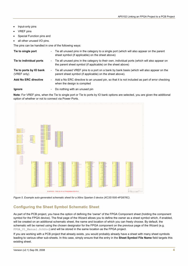
Figure 5. Example auto-generated schematic sheet for a Xilinx Spartan-3 device (XC3S1500-4FG676C).
Configuring the Sheet Symbol Schematic Sheet
As part of the PCB project, you have the option of defining the 'owner' of the FPGA Component sheet (holding the component symbol for the FPGA device). The final page of the Wizard allows you to define the owner as a sheet symbol which, if enabled, will be created on an additional schematic sheet, the name and location of which you can freely choose. By default, the schematic will be named using the chosen designator for the FPGA component on the previous page of the Wizard (e.g. FPGA_U1_Manual.SchDoc) and will be stored in the same location as the FPGA project.
If you are working with a PCB project that already exists, you would probably already have a sheet with many sheet symbols leading to various other sub-sheets. In this case, simply ensure that the entry in the Sheet Symbol File Name field targets this existing sheet.
AP0102 Linking an FPGA Project to a PCB Project
Version (v2.1) Sep 09, 2008 5
In summary, after all of the options in the Wizard have been set as required, the following will be generated:
• A new PCB project (if specified)
• A new schematic sheet, added to the new or existing PCB project, which contains the schematic representation of the FPGA component
• A new schematic sheet with parent sheet symbol (if specified). If an existing sheet is targeted, the parent sheet symbol for the FPGA Component schematic will be added/updated as necessary
• A new configuration (if specified), which will be added to the FPGA project file and which contains a single, new constraint file. The constraint file will contain:
- a part constraint, for example: Record=Constraint | TargetKind=Part | TargetId=XC3S1500-4FG676C
- a PCB board constraint, for example: Record=Constraint | TargetKind=PCB | TargetId=CHC_Accumulator_PCB.PrjPcb
- a list of constraints for all ports on the top-level schematic of the FPGA project. Each of these port constraints is matched (and therefore linked) by net name to the equivalent pin of the FPGA component on the PCB project's auto-generated schematic sheet.
If an existing configuration was chosen, only those elements listed above which are not currently found in any constraint files associated to that configuration, will be added.
For a detailed description of configurations and constraint files, refer to the document AR0124 Design Portability, Configurations and Constraints.
Verifying that the Projects are Linked
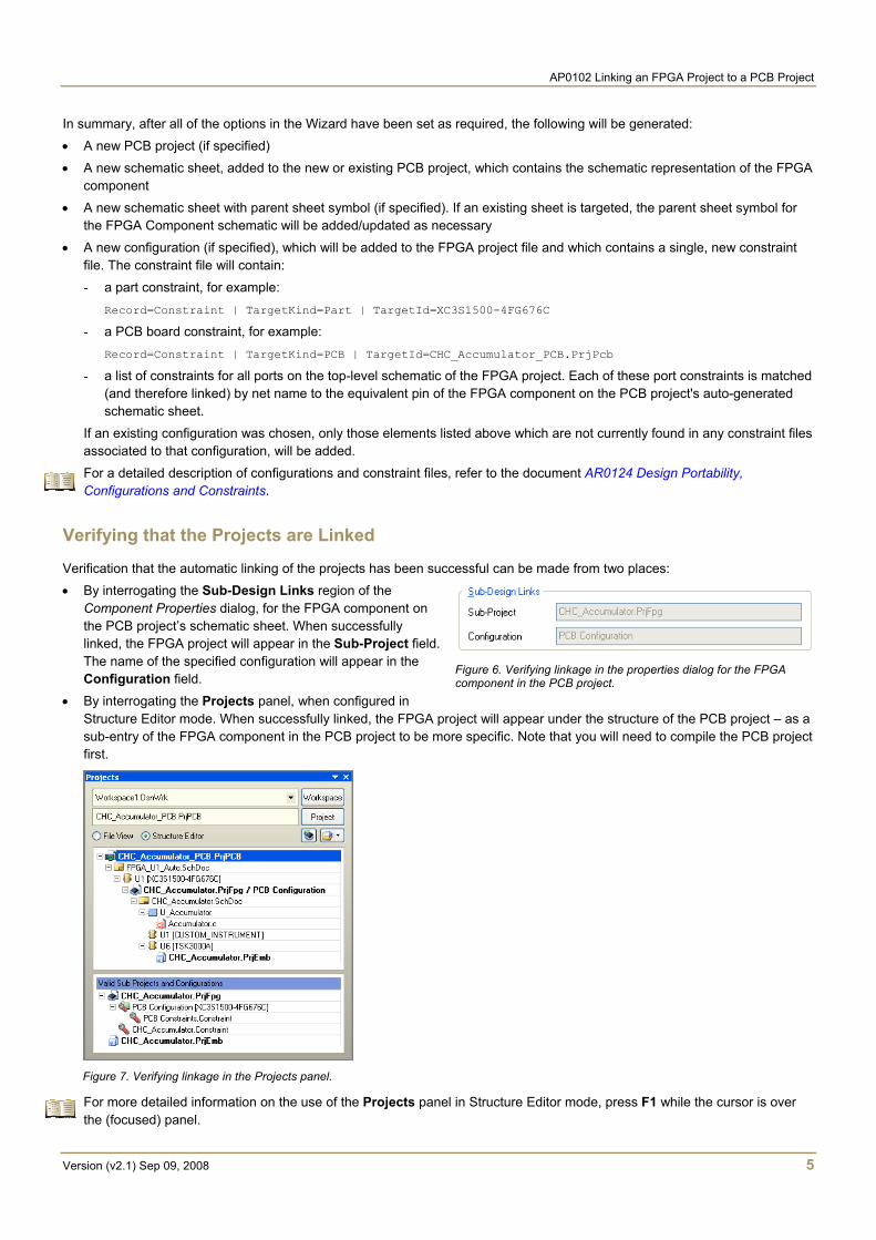
Verification that the automatic linking of the projects has been successful can be made from two places: • By interrogating the Sub-Design Links region of the
Component Properties dialog, for the FPGA component on the PCB project’s schematic sheet. When successfully linked, the FPGA project will appear in the Sub-Project field. The name of the specified configuration will appear in the Configuration field.
• By interrogating the Projects panel, when configured in Structure Editor mode. When successfully linked, the FPGA project will appear under the structure of the PCB project – as a sub-entry of the FPGA component in the PCB project to be more specific. Note that you will need to compile the PCB project first.
Figure 7. Verifying linkage in the Projects panel.
For more detailed information on the use of the Projects panel in Structure Editor mode, press F1 while the cursor is over the (focused) panel.
Figure 6. Verifying linkage in the properties dialog for the FPGA component in the PCB project.
AP0102 Linking an FPGA Project to a PCB Project
Version (v2.1) Sep 09, 2008 6
Manually Linking the FPGA and PCB Projects
The PCB project to which the FPGA design project will be linked can of course be created manually and, quite often, this will be the case, with both projects being designed in parallel.
In such cases, there may not be an auto-generated schematic sheet for the FPGA Component. Linking of the two projects must truly be carried out manually.
Detection of the FPGA Component on the Schematic Sheet
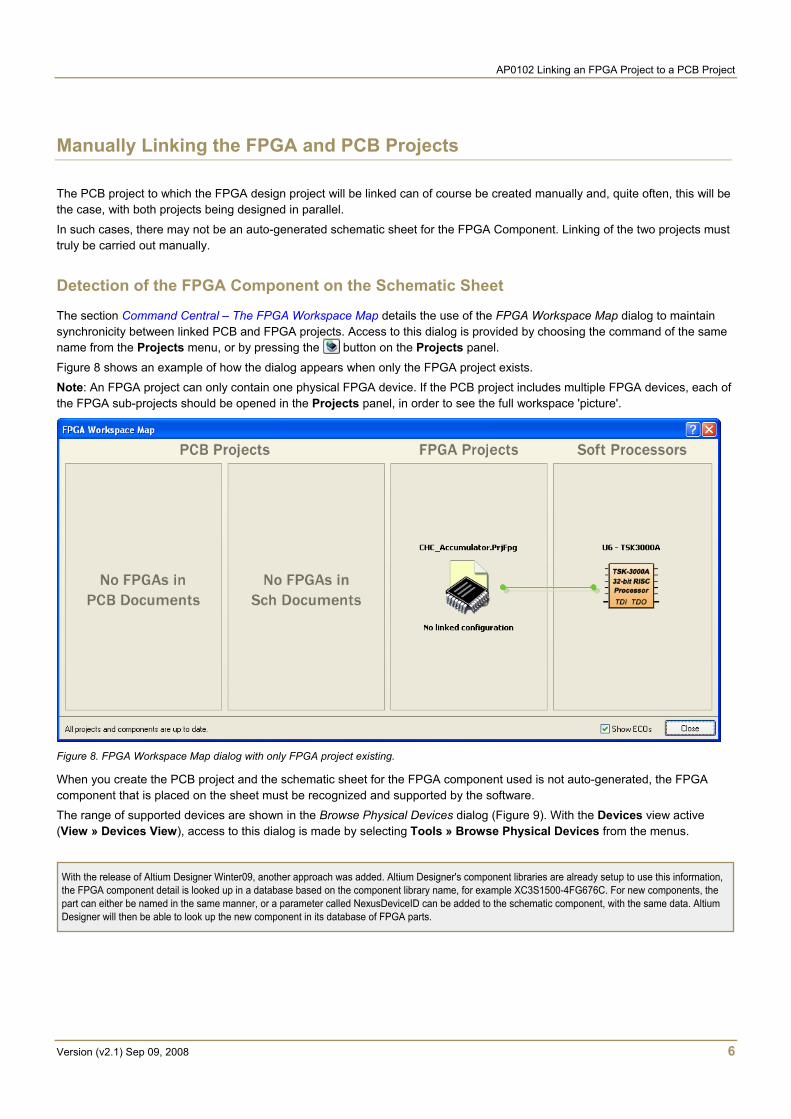
The section Command Central – The FPGA Workspace Map details the use of the FPGA Workspace Map dialog to maintain synchronicity between linked PCB and FPGA projects. Access to this dialog is provided by choosing the command of the same name from the Projects menu, or by pressing the button on the Projects panel.
Figure 8 shows an example of how the dialog appears when only the FPGA project exists. Note: An FPGA project can only contain one physical FPGA device. If the PCB project includes multiple FPGA devices, each of the FPGA sub-projects should be opened in the Projects panel, in order to see the full workspace 'picture'.
Figure 8. FPGA Workspace Map dialog with only FPGA project existing.
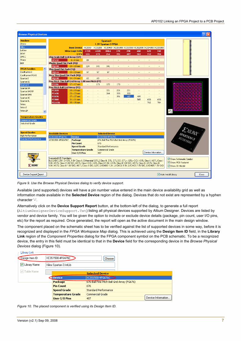
When you create the PCB project and the schematic sheet for the FPGA component used is not auto-generated, the FPGA component that is placed on the sheet must be recognized and supported by the software. The range of supported devices are shown in the Browse Physical Devices dialog (Figure 9). With the Devices view active (View » Devices View), access to this dialog is made by selecting Tools » Browse Physical Devices from the menus.
With the release of Altium Designer Winter09, another approach was added. Altium Designer's component libraries are already setup to use this information, the FPGA component detail is looked up in a database based on the component library name, for example XC3S1500-4FG676C. For new components, the part can either be named in the same manner, or a parameter called NexusDeviceID can be added to the schematic component, with the same data. Altium Designer will then be able to look up the new component in its database of FPGA parts.
AP0102 Linking an FPGA Project to a PCB Project
Version (v2.1) Sep 09, 2008 7
Figure 9. Use the Browse Physical Devices dialog to verify device support.
Available (and supported) devices will have a pin number value entered in the main device availability grid as well as information made available in the Selected Device region of the dialog. Devices that do not exist are represented by a hyphen character ‘-‘. Alternatively click on the Device Support Report button, at the bottom-left of the dialog, to generate a full report (AltiumDesignerDeviceSupport.Txt) listing all physical devices supported by Altium Designer. Devices are listed by vendor and device family. You will be given the option to include or exclude device details (package, pin count, user I/O pins, etc) for the report as required. Once generated, the report will open as the active document in the main design window.
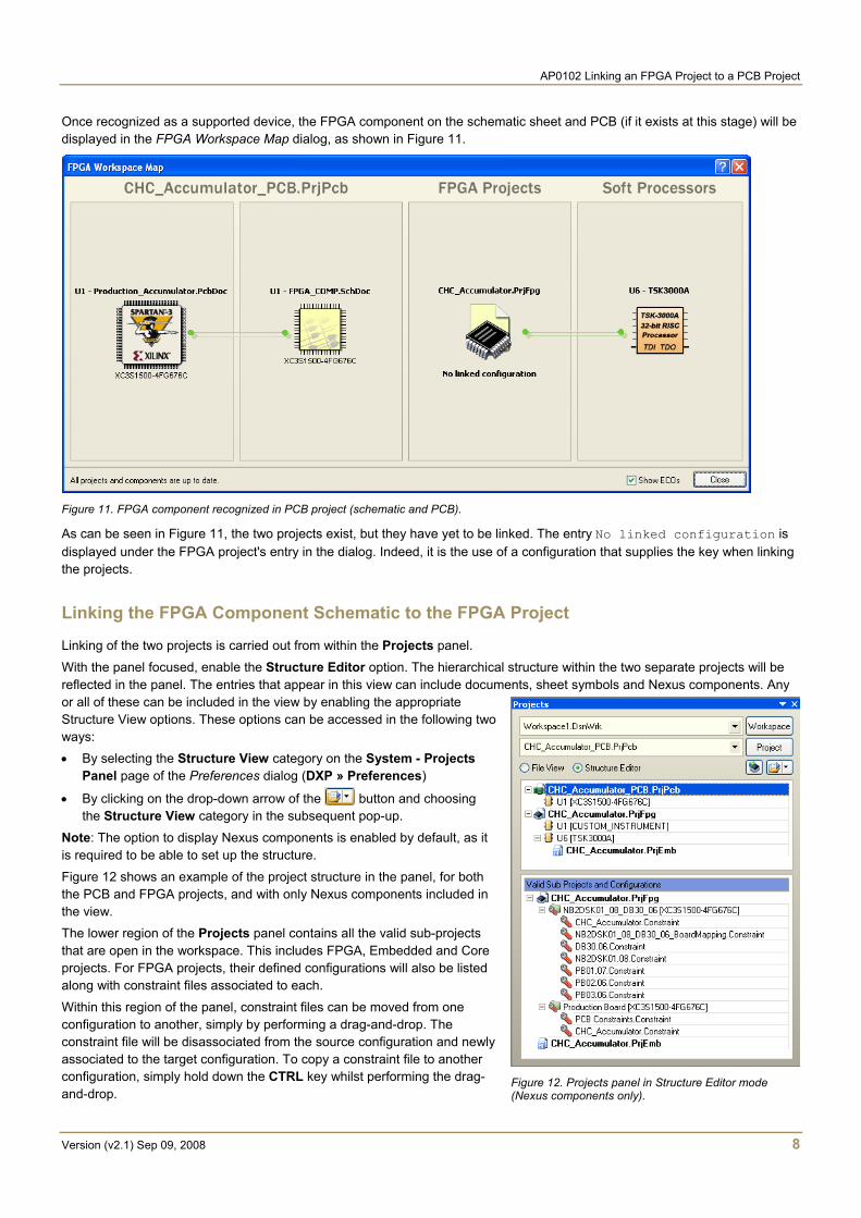
The component placed on the schematic sheet has to be verified against the list of supported devices in some way, before it is recognized and displayed in the FPGA Workspace Map dialog. This is achieved using the Design Item ID field, in the Library Link region of the Component Properties dialog for the FPGA component symbol on the PCB schematic. To be a recognized device, the entry in this field must be identical to that in the Device field for the corresponding device in the Browse Physical Devices dialog (Figure 10).
Figure 10. The placed component is verified using its Design Item ID.
AP0102 Linking an FPGA Project to a PCB Project
Version (v2.1) Sep 09, 2008 8
Once recognized as a supported device, the FPGA component on the schematic sheet and PCB (if it exists at this stage) will be displayed in the FPGA Workspace Map dialog, as shown in Figure 11.
Figure 11. FPGA component recognized in PCB project (schematic and PCB).
As can be seen in Figure 11, the two projects exist, but they have yet to be linked. The entry No linked configuration is displayed under the FPGA project's entry in the dialog. Indeed, it is the use of a configuration that supplies the key when linking the projects.
Linking the FPGA Component Schematic to the FPGA Project
Linking of the two projects is carried out from within the Projects panel.
With the panel focused, enable the Structure Editor option. The hierarchical structure within the two separate projects will be reflected in the panel. The entries that appear in this view can include documents, sheet symbols and Nexus components. Any or all of these can be included in the view by enabling the appropriate Structure View options. These options can be accessed in the following two ways: • By selecting the Structure View category on the System - Projects
Panel page of the Preferences dialog (DXP » Preferences)
• By clicking on the drop-down arrow of the button and choosing the Structure View category in the subsequent pop-up.
Note: The option to display Nexus components is enabled by default, as it is required to be able to set up the structure.
Figure 12 shows an example of the project structure in the panel, for both the PCB and FPGA projects, and with only Nexus components included in the view. The lower region of the Projects panel contains all the valid sub-projects that are open in the workspace. This includes FPGA, Embedded and Core projects. For FPGA projects, their defined configurations will also be listed along with constraint files associated to each.
Within this region of the panel, constraint files can be moved from one configuration to another, simply by performing a drag-and-drop. The constraint file will be disassociated from the source configuration and newly associated to the target configuration. To copy a constraint file to another configuration, simply hold down the CTRL key whilst performing the drag-and-drop.
Figure 12. Projects panel in Structure Editor mode (Nexus components only).

AP0102 Linking an FPGA Project to a PCB Project
Version (v2.1) Sep 09, 2008 9
To purely disassociate a constraint file from a configuration, simply drag the entry for the constraint into free space within the lower region of the panel.
Double-clicking on a configuration entry will launch the Configuration Manager dialog for the parent FPGA project.
Linking of the two projects is achieved in one of the following ways: • Dragging a configuration defined for the FPGA project from the lower region of the Projects panel and dropping it onto the
entry for the FPGA component in the PCB project
• Dragging the FPGA project – from either the upper or lower regions of the panel – and dropping it onto the FPGA component entry in the PCB project
• Right-clicking on the entry for the FPGA component in the PCB project and choosing the Set Sub Project command from the pop-up menu that appears. This will open the Select Sub Project dialog, from where you can browse to and open the desired FPGA sub-project. This method is particularly useful if the desired sub-project is not currently open in the Projects panel.
When using the drag-and-drop methods, the possible FPGA component entries (that reside on schematic sheets within one or more PCB projects) that you can validly drop onto are highlighted in pale blue. As the cursor passes onto a valid 'drop zone' it will change from a no-entry symbol to a document symbol as shown in Figure 13.
Figure 13. Linking projects through drag-and-drop.
If you choose to drag the entire FPGA project entry onto the target schematic FPGA component and more than one valid configuration exists for that project – i.e. more than one configuration contains an associated constraint file targeting the FPGA device – the Select Configuration dialog will appear (Figure 14), from where you can choose which specific configuration to use.
Figure 14. Choose which configuration to use for linking purposes.
AP0102 Linking an FPGA Project to a PCB Project
Version (v2.1) Sep 09, 2008 10
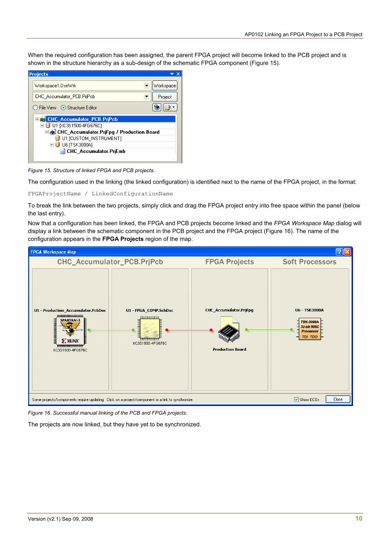
When the required configuration has been assigned, the parent FPGA project will become linked to the PCB project and is shown in the structure hierarchy as a sub-design of the schematic FPGA component (Figure 15).
Figure 15. Structure of linked FPGA and PCB projects.
The configuration used in the linking (the linked configuration) is identified next to the name of the FPGA project, in the format:
FPGAProjectName / LinkedConfigurationName
To break the link between the two projects, simply click and drag the FPGA project entry into free space within the panel (below the last entry).
Now that a configuration has been linked, the FPGA and PCB projects become linked and the FPGA Workspace Map dialog will display a link between the schematic component in the PCB project and the FPGA project (Figure 16). The name of the configuration appears in the FPGA Projects region of the map.
Figure 16. Successful manual linking of the PCB and FPGA projects.
The projects are now linked, but they have yet to be synchronized.

AP0102 Linking an FPGA Project to a PCB Project
Version (v2.1) Sep 09, 2008 11
Synchronizing Manually Linked Projects
Synchronization of the two linked projects is carried out and maintained by establishing a link between the top-level ports in the FPGA project – specified in the relevant constraint file – and the corresponding pins on the FPGA component schematic. Linking is achieved using the signal name. The name given to the port in the FPGA project must be the same as the net label assigned to the corresponding pin of the schematic component in the PCB project.
When you click on the Schematic-FPGA Project link in the FPGA Workspace Map dialog, the Synchronize dialog will appear (Figure 17).
Figure 17. Use the Synchronize dialog to determine changes required to fully synchronize the linked PCB and FPGA projects.
Note: The Synchronize dialog can be accessed irrespective of the state of the link – fully synchronized or out of date.
How the dialog is populated depends on the extent of net naming in the FPGA component schematic. The following is a summary of the possibilities:
• A net label has been assigned to a pin with the same name as that used for the corresponding port in the FPGA project. The pin number is different to that (if specified) in the associated constraint file and/or the electrical type for the pin is different to that of the port. As the port and pin have the same signal name, they will appear in the Matched Signals list. The entry will be highlighted in red as the pin number and/or electrical type is different
• A net label has been assigned to a pin with the same name as that used for the corresponding port in the FPGA project. The pin number is identical to that in the associated constraint file and the electrical type for the pin is identical to that of the port. As the port and pin have the same signal name, they will appear in the Matched Signals list. The entry will be highlighted in green as the pin number and electrical type are also the same
• A net label has been assigned to a pin with a different name to any of the ports in the FPGA project. An entry for the signal name will appear in the Unmatched PCB Signals list.
• All ports that have not been matched to pins with the same name, will appear in the Unmatched FPGA Signals list.
The aim now is to get all ports and pins matched by the same name, pin number and electrical type – i.e. to get the Matched Signals list fully populated and Green.
This is achieved by manually adding and removing nets/ports to/from the PCB project schematic and FPGA project schematic, and changing pin/port electrical properties and pin assignments as required. The Synchronize dialog enables you to create To Do Items so that you can easily remember what needs to be done by checking the To-Do panel.
If the signal naming and electrical types are made identical to start with, the pin numbering can be pushed quickly from one project to the other, depending on whether the master numbering is defined on the PCB or in the constraint file.
AP0102 Linking an FPGA Project to a PCB Project
Version (v2.1) Sep 09, 2008 12
Command Central – The FPGA Workspace Map
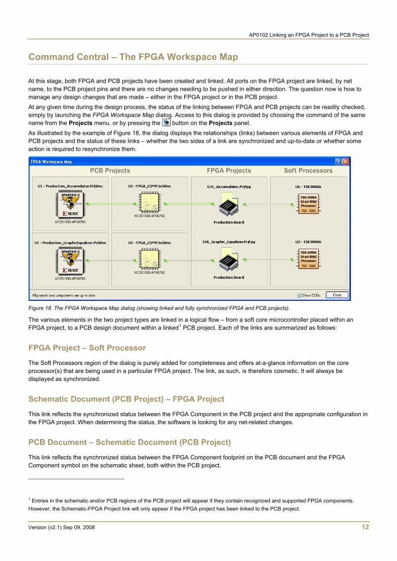
At this stage, both FPGA and PCB projects have been created and linked. All ports on the FPGA project are linked, by net name, to the PCB project pins and there are no changes needing to be pushed in either direction. The question now is how to manage any design changes that are made – either in the FPGA project or in the PCB project.
At any given time during the design process, the status of the linking between FPGA and PCB projects can be readily checked, simply by launching the FPGA Workspace Map dialog. Access to this dialog is provided by choosing the command of the same name from the Projects menu, or by pressing the button on the Projects panel.
As illustrated by the example of Figure 18, the dialog displays the relationships (links) between various elements of FPGA and PCB projects and the status of these links – whether the two sides of a link are synchronized and up-to-date or whether some action is required to resynchronize them.
Figure 18. The FPGA Workspace Map dialog (showing linked and fully synchronized FPGA and PCB projects).
The various elements in the two project types are linked in a logical flow – from a soft core microcontroller placed within an FPGA project, to a PCB design document within a linked1 PCB project. Each of the links are summarized as follows:
FPGA Project – Soft Processor
The Soft Processors region of the dialog is purely added for completeness and offers at-a-glance information on the core processor(s) that are being used in a particular FPGA project. The link, as such, is therefore cosmetic. It will always be displayed as synchronized.
Schematic Document (PCB Project) – FPGA Project
This link reflects the synchronized status between the FPGA Component in the PCB project and the appropriate configuration in the FPGA project. When determining the status, the software is looking for any net-related changes.
PCB Document – Schematic Document (PCB Project)
This link reflects the synchronized status between the FPGA Component footprint on the PCB document and the FPGA Component symbol on the schematic sheet, both within the PCB project.
1 Entries in the schematic and/or PCB regions of the PCB project will appear if they contain recognized and supported FPGA components. However, the Schematic-FPGA Project link will only appear if the FPGA project has been linked to the PCB project.
AP0102 Linking an FPGA Project to a PCB Project
Version (v2.1) Sep 09, 2008 13
A link can appear in one of two colors and hovering over a link will produce a textual description of its status:
- The Green link signifies up to date (i.e. both sides are synchronized). No action is
required.
- The Red link signifies that the two sides of the link are not fully synchronized (i.e. a design
change has been made on one side but has yet to be passed to the other). Clicking on a Schematic-FPGA Project link with this status will open the Synchronize dialog, from where you can browse and match any unmatched ports and pins.
When two elements of the map are shown to be un-synchronized (i.e. the link between them is red), clicking on the link or its associated icons will give access to a number of synchronization options. The hint that appears when hovering over the link will, where possible, provide information on which directions updates should be made in order to achieve synchronization.
Before passing on any design changes over a link, you can view the differences. Changes are made using Engineering Change Orders (ECOs). From within the FPGA Workspace Map dialog, you have full control over what gets updated and when, all from one convenient location.
AP0102 Linking an FPGA Project to a PCB Project
Version (v2.1) Sep 09, 2008 14
Managing Design Changes between linked Projects
The FPGA Workspace Map dialog gives you the ability to check the state of the design across linked FPGA and PCB projects and the means to propagate design changes between the two. The following sections consider some of the more common design changes that might be made and that require use of this dialog to detect such changes and ensure synchronization of the entire design.
In each case, it is assumed that the two, full design projects are local to the designer – stored on the one machine and in the same directory structure.
Configuring I/O Standards
FPGA devices generally support a range of I/O standards. These standards follow industry specifications and often include options like LVTTL, LVCMOS and PCI to name a few. This enables the FPGA to communicate directly with other devices requiring a certain standard. Often the standards will also support further customization including the slew rate, current strength and voltage.
Each device will have its own set of supported standards. Only supported standards can be selected for the current device.
There is a complex set of interactions between different I/O standards in an FPGA. Some I/O standards will be able to co-exist while others are mutually exclusive. Often the requirements are limited to I/O banks, such that all pins within an I/O bank on an FPGA must have compatible I/O standards. This becomes particularly important with voltage referenced standards such as GTL, as an I/O bank will generally only be able to support one voltage reference value.
The interaction of selected I/O standards with one another is not modeled here and vendor documentation should be referred to for more detailed information. As a general rule of thumb, keeping pins using different I/O standards in separate I/O banks will ensure compatibility. Any errors will be picked up when the design is processed by the Vendor Place & Route tools.
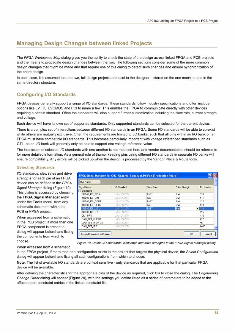
Selecting Standards I/O standards, slew rates and drive strengths for each pin of an FPGA device can be defined in the FPGA Signal Manager dialog (Figure 19). This dialog is accessed by choosing the FPGA Signal Manager entry under the Tools menu, from any schematic document within the PCB or FPGA project.
When accessed from a schematic in the PCB project, if more than one FPGA component is present a dialog will appear beforehand listing the components from which to choose.
When accessed from a schematic in the FPGA project, if more than one configuration exists in the project that targets the physical device, the Select Configuration dialog will appear beforehand listing all such configurations from which to choose. Note: The list of available I/O standards are context sensitive - only standards that are applicable for that particular FPGA device will be available. After defining the characteristics for the appropriate pins of the device as required, click OK to close the dialog. The Engineering Change Order dialog will appear (Figure 20), with the settings you define listed as a series of parameters to be added to the affected port constraint entries in the linked constraint file.
Figure 19. Define I/O standards, slew rates and drive strengths in the FPGA Signal Manager dialog.
AP0102 Linking an FPGA Project to a PCB Project
Version (v2.1) Sep 09, 2008 15
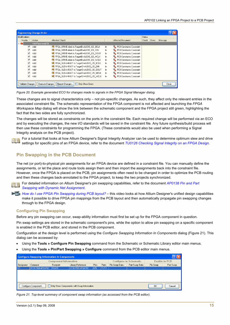
Figure 20. Example generated ECO for changes made to signals in the FPGA Signal Manager dialog.
These changes are to signal characteristics only – not pin-specific changes. As such, they affect only the relevant entries in the associated constraint file. The schematic representation of the FPGA component is not affected and launching the FPGA Workspace Map dialog will show the link between the schematic component and the FPGA project still green, highlighting the fact that the two sides are fully synchronized.
The changes will be stored as constraints on the ports in the constraint file. Each required change will be performed via an ECO and by executing the changes, the new I/O standards will be saved in the constraint file. Any future synthesis/build process will then use these constraints for programming the FPGA. (These constraints would also be used when performing a Signal Integrity analysis on the PCB project).
For a tutorial that looks at how Altium Designer's Signal Integrity Analyzer can be used to determine optimum slew and drive settings for specific pins of an FPGA device, refer to the document TU0126 Checking Signal Integrity on an FPGA Design.
Pin Swapping in the PCB Document
The net (or port)-to-physical pin assignments for an FPGA device are defined in a constraint file. You can manually define the assignments, or let the place and route tools assign them and then import the assignments back into the constraint file. However, once the FPGA is placed on the PCB, pin assignments often need to be changed in order to optimize the PCB routing and then these changes back-annotated to the FPGA project, to keep the two projects synchronized.
For detailed information on Altium Designer's pin swapping capabilities, refer to the document AP0138 Pin and Part Swapping with Dynamic Net Assignment.
How do I use FPGA Pin Swapping during PCB layout? – this video looks at how Altium Designer's unified design capabilities make it possible to drive FPGA pin mappings from the PCB layout and then automatically propagate pin swapping changes through to the FPGA design.
Configuring Pin Swapping Before any pin swapping can occur, swap-ability information must first be set up for the FPGA component in question.
Pin swap settings are stored in the schematic component's pins, while the option to allow pin swapping on a specific component is enabled in the PCB editor, and stored in the PCB component.
Configuration at the design level is performed using the Configure Swapping Information In Components dialog (Figure 21). This dialog can be accessed by: • Using the Tools » Configure Pin Swapping command from the Schematic or Schematic Library editor main menus.
• Using the Tools » Pin/Part Swapping » Configure command from the PCB editor main menus.
Figure 21. Top-level summary of component swap information (as accessed from the PCB editor).
AP0102 Linking an FPGA Project to a PCB Project
Version (v2.1) Sep 09, 2008 16
The dialog lists all components in the design (or library) along with their current swap settings. Double-clicking on a component entry will give access to the Configure Pin Swapping dialog for that component, from where you can define the swap settings for pin swapping accordingly. Alternatively, access the dialog directly for a given component by right-clicking on that component in the schematic or PCB workspace and choosing the command to configure pin swapping from the Part Actions or Component Actions context menu respectively.
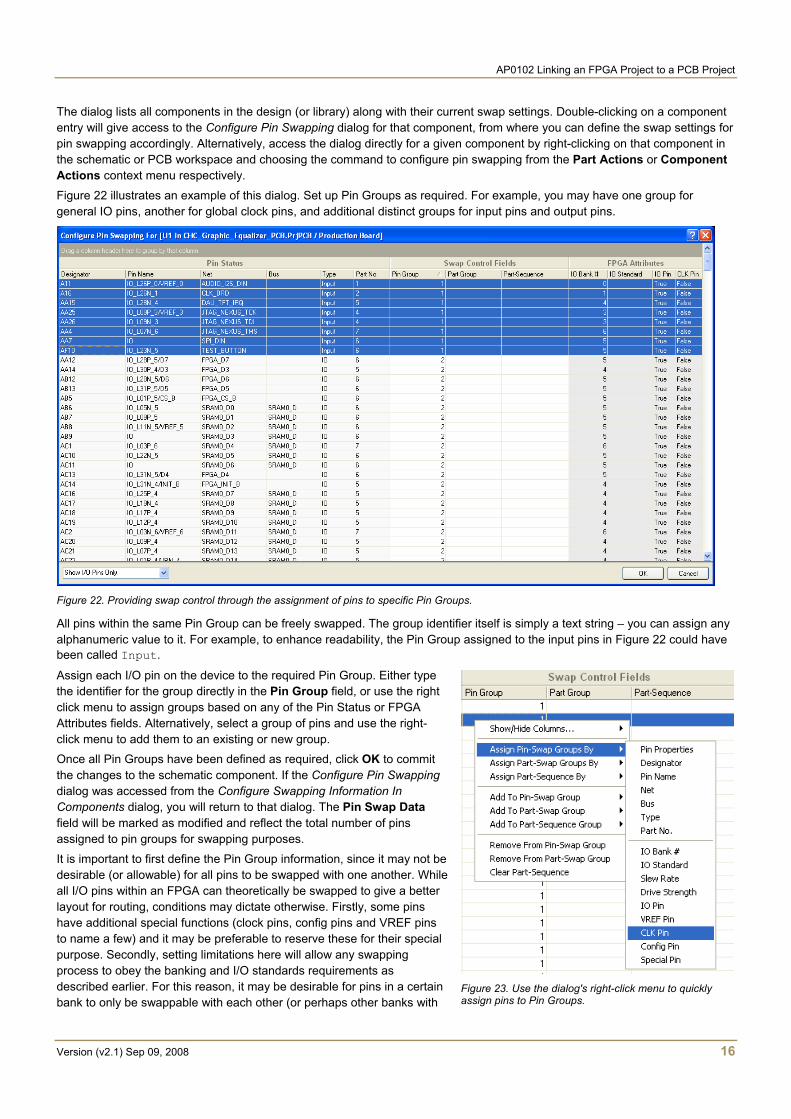
Figure 22 illustrates an example of this dialog. Set up Pin Groups as required. For example, you may have one group for general IO pins, another for global clock pins, and additional distinct groups for input pins and output pins.
Figure 22. Providing swap control through the assignment of pins to specific Pin Groups.
All pins within the same Pin Group can be freely swapped. The group identifier itself is simply a text string – you can assign any alphanumeric value to it. For example, to enhance readability, the Pin Group assigned to the input pins in Figure 22 could have been called Input.
Assign each I/O pin on the device to the required Pin Group. Either type the identifier for the group directly in the Pin Group field, or use the right click menu to assign groups based on any of the Pin Status or FPGA Attributes fields. Alternatively, select a group of pins and use the right-click menu to add them to an existing or new group. Once all Pin Groups have been defined as required, click OK to commit the changes to the schematic component. If the Configure Pin Swapping dialog was accessed from the Configure Swapping Information In Components dialog, you will return to that dialog. The Pin Swap Data field will be marked as modified and reflect the total number of pins assigned to pin groups for swapping purposes.
It is important to first define the Pin Group information, since it may not be desirable (or allowable) for all pins to be swapped with one another. While all I/O pins within an FPGA can theoretically be swapped to give a better layout for routing, conditions may dictate otherwise. Firstly, some pins have additional special functions (clock pins, config pins and VREF pins to name a few) and it may be preferable to reserve these for their special purpose. Secondly, setting limitations here will allow any swapping process to obey the banking and I/O standards requirements as described earlier. For this reason, it may be desirable for pins in a certain bank to only be swappable with each other (or perhaps other banks with
Figure 23. Use the dialog's right-click menu to quickly assign pins to Pin Groups.

AP0102 Linking an FPGA Project to a PCB Project
Version (v2.1) Sep 09, 2008 17
compatible I/O standards).
Enabling Pin Swapping As mentioned earlier, pin swapping is enabled on the PCB side. This is performed using one of the following methods: • Access the Configure Swapping Information In Components dialog (Tools » Pin/Part Swapping » Configure), and enable
the Pin Swap option for the required component.
• Access the properties dialog for the PCB component footprint. In the Swapping Options region, enable the Enable Pin Swaps option.
• Select the component footprint in the workspace and enable the Enable Pin Swapping option, using either the PCB Inspector or PCB List panels.
In addition to enabling pin swapping, you must also specify the method(s) used to execute the swapping with respect to the FPGA component on the schematic (in the PCB project). These can be found on the Options tab of the Options for PCB Project dialog (Project » Project Options) and are illustrated in Figure 24.
Both options are enabled by default, although it is advisable to disable the Changing Schematic Pins option. Use of this option is more of a 'hardwired' approach and does not lend itself to future updates of the schematic symbol from the source library. The Adding / Removing Net Labels option is far more suited to FPGA components and essentially just means that net labels are swapped, rather than the pins themselves. (Note that this is only possible provided that connectivity to the pins of the FPGA on the schematic is made using net labels, and not fixed wiring!).
Performing Pin Swapping Having defined the Pin Groups as appropriate and enabled pin swapping for the required components, the actual process of swapping pins can now be performed. With the PCB document active, pin swapping tools are available from the Tools » Pin/Part Swapping sub-menu.
Figure 24. Define method(s) by which pin swapping is executed on the schematic.
AP0102 Linking an FPGA Project to a PCB Project
Version (v2.1) Sep 09, 2008 18
It is advisable to have the linked FPGA and PCB projects fully synchronized prior to performing any pin swapping operations on the PCB. This allows subsequent pin swap data to be passed between projects in a pain-free, efficient fashion.
During a pin swap operation, Altium Designer analyses the net assigned to the chosen pin and dynamically reassigns the net on any connected routing as well as the pin. This level of functionality means that partially routed nets and pre-routed multilayer escapes from complex BGA devices can be swapped. Differential pairs can also be swapped, taking advantage of the knowledge about differential pin-pairs on FPGAs.
Automatic pin swapping can be carried out for any or all FPGA components in a document, dependent on whether pin swapping is enabled for those components or not. This functionality is provided courtesy of a powerful automatic Optimizer, invoked using the Automatic Net/Pin Optimizer command.
The Optimizer uses a two-stage process – a Fast optimization pass followed by an Iterative pass. You have control over whether to run the iterative pass, but generally it is a good idea to do so in order to achieve optimum results.
The Optimizer will attempt to find the optimal pin allocations for routing, while obeying the defined Pin Group settings. The total routing length and the number of net crossovers are key factors when routing the PCB, and the optimizer will focus on keeping both the routing length and the number of crossovers down to a minimum.
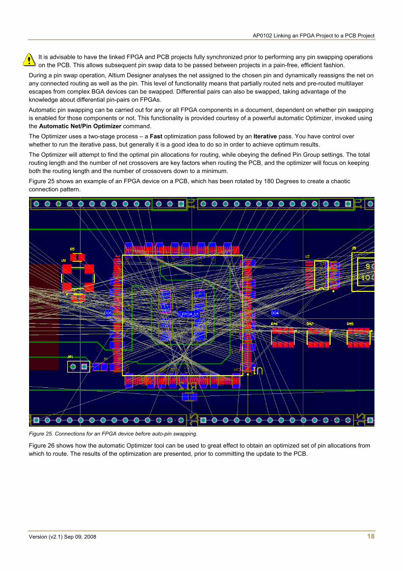
Figure 25 shows an example of an FPGA device on a PCB, which has been rotated by 180 Degrees to create a chaotic connection pattern.
Figure 25. Connections for an FPGA device before auto-pin swapping.
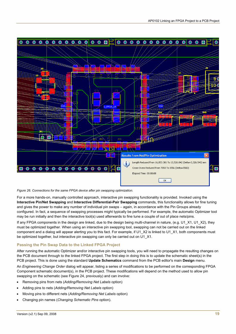
Figure 26 shows how the automatic Optimizer tool can be used to great effect to obtain an optimized set of pin allocations from which to route. The results of the optimization are presented, prior to committing the update to the PCB.
AP0102 Linking an FPGA Project to a PCB Project
Version (v2.1) Sep 09, 2008 19
Figure 26. Connections for the same FPGA device after pin swapping optimization.
For a more hands-on, manually controlled approach, interactive pin swapping functionality is provided. Invoked using the Interactive Pin/Net Swapping and Interactive Differential-Pair Swapping commands, this functionality allows for fine tuning and gives the power to make any number of individual pin swaps – again, in accordance with the Pin Groups already configured. In fact, a sequence of swapping processes might typically be performed. For example, the automatic Optimizer tool may be run initially and then the interactive tool(s) used afterwards to fine tune a couple of out of place nets/pins.
If any FPGA components in the design are linked, due to the design being multi-channel in nature, (e.g. U1_X1, U1_X2), they must be optimized together. When using an interactive pin swapping tool, swapping can not be carried out on the linked component and a dialog will appear alerting you to this fact. For example, if U1_X2 is linked to U1_X1, both components must be optimized together, but interactive pin swapping can only be carried out on U1_X1.
Passing the Pin Swap Data to the Linked FPGA Project After running the automatic Optimizer and/or interactive pin swapping tools, you will need to propagate the resulting changes on the PCB document through to the linked FPGA project. The first step in doing this is to update the schematic sheet(s) in the PCB project. This is done using the standard Update Schematics command from the PCB editor's main Design menu.
An Engineering Change Order dialog will appear, listing a series of modifications to be performed on the corresponding FPGA Component schematic document(s), in the PCB project. These modifications will depend on the method used to allow pin swapping on the schematic (see Figure 24, previously) and can involve:
• Removing pins from nets (Adding/Removing Net Labels option)
• Adding pins to nets (Adding/Removing Net Labels option)
• Moving pins to different nets (Adding/Removing Net Labels option)
• Changing pin names (Changing Schematic Pins option).
AP0102 Linking an FPGA Project to a PCB Project
Version (v2.1) Sep 09, 2008 20
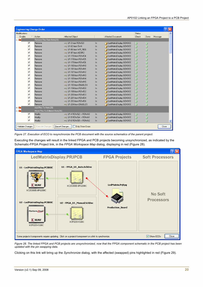
Figure 27. Execution of ECO to resynchronize the PCB document with the source schematics of the parent project.
Executing the changes will result in the linked FPGA and PCB projects becoming unsynchronized, as indicated by the Schematic-FPGA Project link, in the FPGA Workspace Map dialog, displaying in red (Figure 28).
Figure 28. The linked FPGA and PCB projects are unsynchronized, now that the FPGA component schematic in the PCB project has been updated with the pin swapping data.
Clicking on this link will bring up the Synchronize dialog, with the affected (swapped) pins highlighted in red (Figure 29).
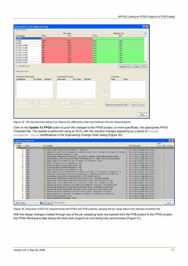
AP0102 Linking an FPGA Project to a PCB Project
Version (v2.1) Sep 09, 2008 21
Figure 29. The Synchronize dialog now reflects the differences that exist between the two linked projects.
Click on the Update To FPGA button to push the changes to the FPGA project, or more specifically, the appropriate FPGA Constraint file. The update is performed using an ECO, with the required changes appearing as a series of Change Parameter Value modifications in the Engineering Change Order dialog (Figure 30).
Figure 30. Execution of ECO to resynchronize the FPGA and PCB projects, passing the pin swap data to the relevant constraint file.
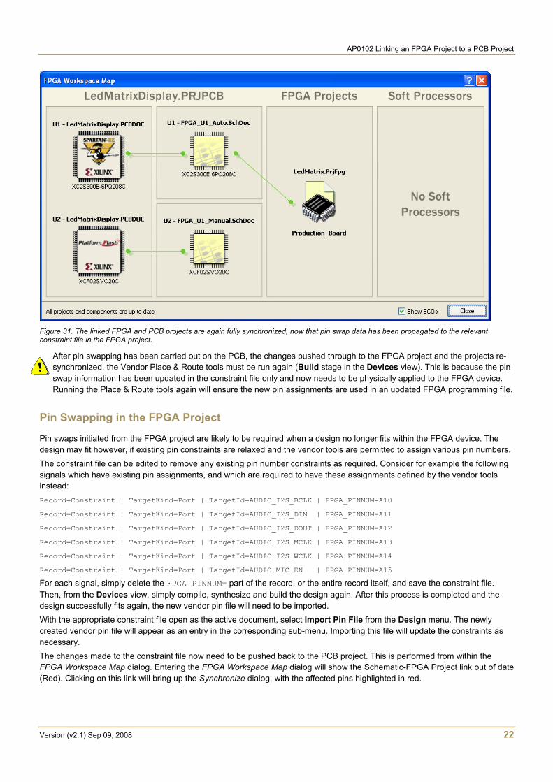
With the design changes created through use of the pin swapping tools now passed from the PCB project to the FPGA project, the FPGA Workspace Map dialog will show both projects as now being fully synchronized (Figure 31).
AP0102 Linking an FPGA Project to a PCB Project
Version (v2.1) Sep 09, 2008 22
Figure 31. The linked FPGA and PCB projects are again fully synchronized, now that pin swap data has been propagated to the relevant constraint file in the FPGA project.
After pin swapping has been carried out on the PCB, the changes pushed through to the FPGA project and the projects re-synchronized, the Vendor Place & Route tools must be run again (Build stage in the Devices view). This is because the pin swap information has been updated in the constraint file only and now needs to be physically applied to the FPGA device. Running the Place & Route tools again will ensure the new pin assignments are used in an updated FPGA programming file.
Pin Swapping in the FPGA Project
Pin swaps initiated from the FPGA project are likely to be required when a design no longer fits within the FPGA device. The design may fit however, if existing pin constraints are relaxed and the vendor tools are permitted to assign various pin numbers.
The constraint file can be edited to remove any existing pin number constraints as required. Consider for example the following signals which have existing pin assignments, and which are required to have these assignments defined by the vendor tools instead: Record=Constraint | TargetKind=Port | TargetId=AUDIO_I2S_BCLK | FPGA_PINNUM=A10
Record=Constraint | TargetKind=Port | TargetId=AUDIO_I2S_DIN | FPGA_PINNUM=A11
Record=Constraint | TargetKind=Port | TargetId=AUDIO_I2S_DOUT | FPGA_PINNUM=A12
Record=Constraint | TargetKind=Port | TargetId=AUDIO_I2S_MCLK | FPGA_PINNUM=A13
Record=Constraint | TargetKind=Port | TargetId=AUDIO_I2S_WCLK | FPGA_PINNUM=A14
Record=Constraint | TargetKind=Port | TargetId=AUDIO_MIC_EN | FPGA_PINNUM=A15
For each signal, simply delete the FPGA_PINNUM= part of the record, or the entire record itself, and save the constraint file. Then, from the Devices view, simply compile, synthesize and build the design again. After this process is completed and the design successfully fits again, the new vendor pin file will need to be imported. With the appropriate constraint file open as the active document, select Import Pin File from the Design menu. The newly created vendor pin file will appear as an entry in the corresponding sub-menu. Importing this file will update the constraints as necessary.
The changes made to the constraint file now need to be pushed back to the PCB project. This is performed from within the FPGA Workspace Map dialog. Entering the FPGA Workspace Map dialog will show the Schematic-FPGA Project link out of date (Red). Clicking on this link will bring up the Synchronize dialog, with the affected pins highlighted in red.
AP0102 Linking an FPGA Project to a PCB Project
Version (v2.1) Sep 09, 2008 23
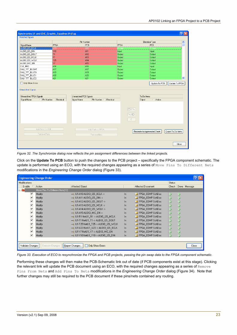
Figure 32. The Synchronize dialog now reflects the pin assignment differences between the linked projects.
Click on the Update To PCB button to push the changes to the PCB project – specifically the FPGA component schematic. The update is performed using an ECO, with the required changes appearing as a series of Move Pins To Different Nets modifications in the Engineering Change Order dialog (Figure 33).
Figure 33. Execution of ECO to resynchronize the FPGA and PCB projects, passing the pin swap data to the FPGA component schematic.
Performing these changes will then make the PCB-Schematic link out of date (if PCB components exist at this stage). Clicking the relevant link will update the PCB document using an ECO, with the required changes appearing as a series of Remove Pins From Nets and Add Pins To Nets modifications in the Engineering Change Order dialog (Figure 34). Note that further changes may still be required to the PCB document if these pins/nets contained any routing.
AP0102 Linking an FPGA Project to a PCB Project
Version (v2.1) Sep 09, 2008 24
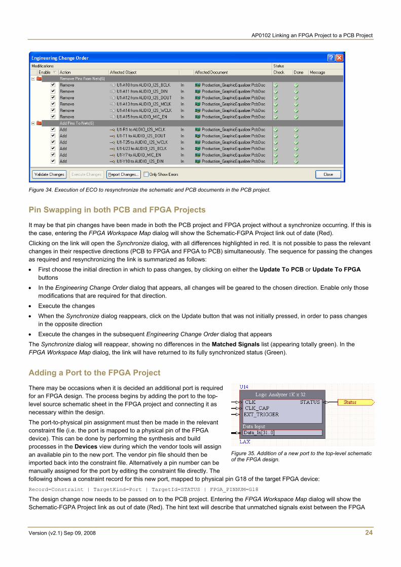
Figure 34. Execution of ECO to resynchronize the schematic and PCB documents in the PCB project.
Pin Swapping in both PCB and FPGA Projects
It may be that pin changes have been made in both the PCB project and FPGA project without a synchronize occurring. If this is the case, entering the FPGA Workspace Map dialog will show the Schematic-FGPA Project link out of date (Red).
Clicking on the link will open the Synchronize dialog, with all differences highlighted in red. It is not possible to pass the relevant changes in their respective directions (PCB to FPGA and FPGA to PCB) simultaneously. The sequence for passing the changes as required and resynchronizing the link is summarized as follows: • First choose the initial direction in which to pass changes, by clicking on either the Update To PCB or Update To FPGA
buttons
• In the Engineering Change Order dialog that appears, all changes will be geared to the chosen direction. Enable only those modifications that are required for that direction.
• Execute the changes
• When the Synchronize dialog reappears, click on the Update button that was not initially pressed, in order to pass changes in the opposite direction
• Execute the changes in the subsequent Engineering Change Order dialog that appears The Synchronize dialog will reappear, showing no differences in the Matched Signals list (appearing totally green). In the FPGA Workspace Map dialog, the link will have returned to its fully synchronized status (Green).
Adding a Port to the FPGA Project
There may be occasions when it is decided an additional port is required for an FPGA design. The process begins by adding the port to the top-level source schematic sheet in the FPGA project and connecting it as necessary within the design.
The port-to-physical pin assignment must then be made in the relevant constraint file (i.e. the port is mapped to a physical pin of the FPGA device). This can be done by performing the synthesis and build processes in the Devices view during which the vendor tools will assign an available pin to the new port. The vendor pin file should then be imported back into the constraint file. Alternatively a pin number can be manually assigned for the port by editing the constraint file directly. The following shows a constraint record for this new port, mapped to physical pin G18 of the target FPGA device: Record=Constraint | TargetKind=Port | TargetId=STATUS | FPGA_PINNUM=G18
The design change now needs to be passed on to the PCB project. Entering the FPGA Workspace Map dialog will show the Schematic-FGPA Project link as out of date (Red). The hint text will describe that unmatched signals exist between the FPGA
Figure 35. Addition of a new port to the top-level schematic of the FPGA design.
AP0102 Linking an FPGA Project to a PCB Project
Version (v2.1) Sep 09, 2008 25
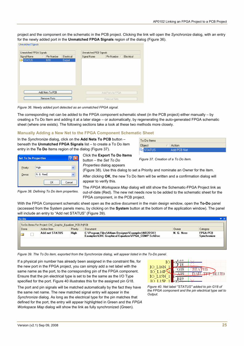
project and the component on the schematic in the PCB project. Clicking the link will open the Synchronize dialog, with an entry for the newly added port in the Unmatched FPGA Signals region of the dialog (Figure 36).
Figure 36. Newly added port detected as an unmatched FPGA signal.
The corresponding net can be added to the FPGA component schematic sheet (in the PCB project) either manually – by creating a To Do Item and adding it at a later stage – or automatically, by regenerating the auto-generated FPGA schematic sheet (where one exists). The following sections take a look at these two methods more closely.
Manually Adding a New Net to the FPGA Component Schematic Sheet In the Synchronize dialog, click on the Add Nets To PCB button – beneath the Unmatched FPGA Signals list – to create a To Do item entry in the To Do Items region of the dialog (Figure 37).
Click the Export To Do Items button – the Set To Do Properties dialog appears (Figure 38). Use this dialog to set a Priority and nominate an Owner for the item. After clicking OK, the new To Do Item will be written and a confirmation dialog will appear to verify this.
The FPGA Workspace Map dialog will still show the Schematic-FPGA Project link as out-of-date (Red). The new net needs now to be added to the schematic sheet for the FPGA component, in the PCB project.
With the FPGA Component schematic sheet open as the active document in the main design window, open the To-Do panel (accessed from the System panels menu, by clicking on the System button at the bottom of the application window). The panel will include an entry to “Add net STATUS” (Figure 39).
Figure 39. The To Do item, exported from the Synchronize dialog, will appear listed in the To-Do panel.
If a physical pin number has already been assigned in the constraint file, for the new port in the FPGA project, you can simply add a net label with the same name as the port, to the corresponding pin of the FPGA component. Ensure that the pin electrical type is set to be the same as the I/O Type specified for the port. Figure 40 illustrates this for the assigned pin G18.
The port and pin signals will be matched automatically by the fact they have the same net name. The new matched signal entry will appear in the Synchronize dialog. As long as the electrical type for the pin matches that defined for the port, the entry will appear highlighted in Green and the FPGA Workspace Map dialog will show the link as fully synchronized (Green).
Figure 37. Creation of a To Do item.
Figure 38. Defining To Do item properties.
Figure 40. Net label "STATUS" added to pin G18 of the FPGA component and the pin electrical type set to Output.
AP0102 Linking an FPGA Project to a PCB Project
Version (v2.1) Sep 09, 2008 26
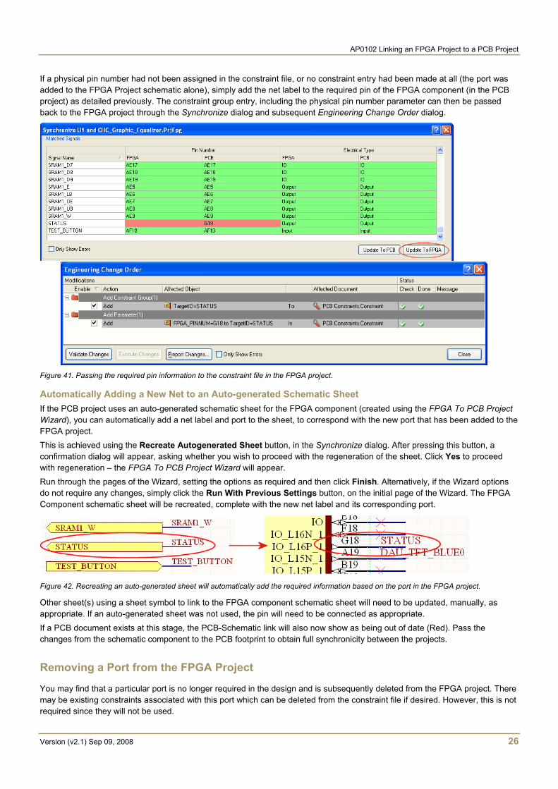
If a physical pin number had not been assigned in the constraint file, or no constraint entry had been made at all (the port was added to the FPGA Project schematic alone), simply add the net label to the required pin of the FPGA component (in the PCB project) as detailed previously. The constraint group entry, including the physical pin number parameter can then be passed back to the FPGA project through the Synchronize dialog and subsequent Engineering Change Order dialog.
Figure 41. Passing the required pin information to the constraint file in the FPGA project.
Automatically Adding a New Net to an Auto-generated Schematic Sheet If the PCB project uses an auto-generated schematic sheet for the FPGA component (created using the FPGA To PCB Project Wizard), you can automatically add a net label and port to the sheet, to correspond with the new port that has been added to the FPGA project. This is achieved using the Recreate Autogenerated Sheet button, in the Synchronize dialog. After pressing this button, a confirmation dialog will appear, asking whether you wish to proceed with the regeneration of the sheet. Click Yes to proceed with regeneration – the FPGA To PCB Project Wizard will appear. Run through the pages of the Wizard, setting the options as required and then click Finish. Alternatively, if the Wizard options do not require any changes, simply click the Run With Previous Settings button, on the initial page of the Wizard. The FPGA Component schematic sheet will be recreated, complete with the new net label and its corresponding port.
Figure 42. Recreating an auto-generated sheet will automatically add the required information based on the port in the FPGA project.
Other sheet(s) using a sheet symbol to link to the FPGA component schematic sheet will need to be updated, manually, as appropriate. If an auto-generated sheet was not used, the pin will need to be connected as appropriate.
If a PCB document exists at this stage, the PCB-Schematic link will also now show as being out of date (Red). Pass the changes from the schematic component to the PCB footprint to obtain full synchronicity between the projects.
Removing a Port from the FPGA Project
You may find that a particular port is no longer required in the design and is subsequently deleted from the FPGA project. There may be existing constraints associated with this port which can be deleted from the constraint file if desired. However, this is not required since they will not be used.
AP0102 Linking an FPGA Project to a PCB Project
Version (v2.1) Sep 09, 2008 27
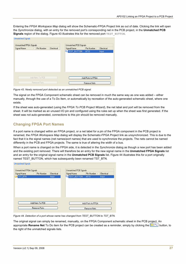
Entering the FPGA Workspace Map dialog will show the Schematic-FPGA Project link as out of date. Clicking the link will open the Synchronize dialog, with an entry for the removed port’s corresponding net in the PCB project, in the Unmatched PCB Signals region of the dialog. Figure 43 illustrates this for the removed port TEST_BUTTON.
Figure 43. Newly removed port detected as an unmatched PCB signal.
The signal on the FPGA Component schematic sheet can be removed in much the same way as one was added – either manually, through the use of a To Do Item, or automatically by recreation of the auto-generated schematic sheet, where one exists.
If the sheet was auto-generated (using the FPGA To PCB Project Wizard), the net label and port will be removed from the sheet. It will be marked as an unused I/O pin and configured using the rules set up when the sheet was first generated. If the sheet was not auto-generated, connections to this pin should be removed manually.
Changing FPGA Port Names
If a port name is changed within an FPGA project, or a net label for a pin of the FPGA component in the PCB project is renamed, the FPGA Workspace Map dialog will display the Schematic-FPGA Project link as unsynchronized. This is due to the fact that it is the signal names (net names/port names) that are used to synchronize the projects. The nets cannot be named differently in the PCB and FPGA projects. The same is true of altering the width of a bus.
When a port name is changed on the FPGA side, it is detected in the Synchronize dialog as though a new port has been added and the existing port removed. There will therefore be an entry for the new signal name in the Unmatched FPGA Signals list and an entry for the original signal name in the Unmatched PCB Signals list. Figure 44 illustrates this for a port originally named TEST_BUTTON, which has subsequently been renamed TST_BTN.
Figure 44. Detection of a port whose name has changed from TEST_BUTTON to TST_BTN.
The original signal can simply be renamed, manually, on the FPGA Component schematic sheet in the PCB project. An appropriate Rename Net To Do item for the PCB project can be created as a reminder, simply by clicking the button, to the right of the unmatched signals lists.
AP0102 Linking an FPGA Project to a PCB Project
Version (v2.1) Sep 09, 2008 28
In a similar fashion when a net label is renamed for a component pin on the PCB side, it is detected in the Synchronize dialog as though a new net has been added and the existing net removed. There will therefore be an entry for the new signal name in the Unmatched PCB Signals list and an entry for the original signal name in the Unmatched FPGA Signals list.
The original signal can simply be renamed, manually, on the top-level sheet of the FPGA project. An appropriate Rename Port To Do item for the FPGA project can be created as a reminder, simply by clicking the button, to the right of the unmatched signals lists.
Changing FPGA Devices
At some point during the design process, it is quite possible that the desired target FPGA device may change. A larger device might be required or a decision to change vendors might be made.
As a first step, the process outlined in the section Automatically Linking the FPGA and PCB Projects should be followed. If the FPGA To PCB Project Wizard is used, a new bottom level, auto-generated schematic sheet will be created.
The old sheet – generated based on the previous target device - can then be removed. The sheet symbol for the old sheet should be replaced with that for the new sheet. It is likely that these sheet symbols will be very similar since most ports will likely be in common. Obviously the more fundamental the change of device, the larger scale the changes are likely to be throughout the schematic. Using the traditional Update PCB command from the Design menu in the schematic, the new component can then be placed on the PCB, if one exists. Then, with the new FPGA target device in place in both FPGA and PCB projects, it is a simple matter of referring to the FPGA Workspace Map dialog to ensure that the projects remain synchronized and any further design changes are passed through the relevant links accordingly.
AP0102 Linking an FPGA Project to a PCB Project
Version (v2.1) Sep 09, 2008 29
Managing Design Changes using a Stub FPGA Project
It is often the case that the PCB and FPGA projects are not designed by the same person. Indeed, they might not be developed on the same computer or even in the same locale. In such cases, a method of passing design changes between projects is needed, whereby only relevant information is passed, without the need to send the entire project – PCB or FPGA – back and forth between locations and designers. The answer to remote development of projects that need to be kept synchronized, with a view to bringing them together at a future date, is the Stub.
The Stub is essentially a satellite FPGA project that is initially produced by the PCB designer. It is used to pass changes made to the PCB project on to the FPGA designer, who imports changes from the Stub FPGA project into the full FPGA design project. Any changes made by the FPGA designer are passed back into the stub, which in turn is sent back to the PCB designer who, to all intents and purposes, treats the Stub as if it were the real, full-blown FPGA project.
Figure 45 illustrates the two processes of maintaining design changes between linked PCB and FPGA projects – with and without the use of a Stub FPGA project.
Figure 45. Use of a Stub FPGA project to keep remote projects synchronized.
The name Stub does not actually appear anywhere, rather it is a term of reference used to reflect the fact that the schematic sheet in the FPGA project does not contain a complete design – no FPGA components, processors, virtual instruments, or wiring – it simply contains the top-levels ports for the full FPGA design.
Creating a Stub FPGA Project
The Stub FPGA project can be created in one of two ways:
• By running the PCB To FPGA Project Wizard
• As a result of changing signal characteristics within the PCB project
The following sections take a closer look at the creation of the Stub FPGA project in these two cases.
Running the Wizard With the FPGA Component schematic document in the PCB project open as the active view in the main design window, simply choose the PCB To FPGA Project Wizard entry on the Tools menu. The Wizard will appear (Figure 46).
Import FPGA Project Changes
FPGA Workspace
FPGA Workspace
PCB Design Project
PCB Design Project
FPGA Design Project
FPGA Master Design Project
Stub FPGA Project

AP0102 Linking an FPGA Project to a PCB Project
Version (v2.1) Sep 09, 2008 30
Figure 46. PCB To FPGA Project Wizard.
Selecting the FPGA Component The second page of the Wizard enables you to choose which FPGA component in the PCB project (if there are more than one) to be used when generating the FPGA project. Simply select the required component and click Next>.
Configuring the FPGA Project The next page of the Wizard enables you to define where, and under what name, the FPGA project will be stored. By default, the project will have the name FPGA Project1.PrjFpg and will be stored in the same location as the PCB project.
From this page of the Wizard, you can also define the name of the top-level schematic sheet in the FPGA project. Define the name and location for this sheet as required. By default, the sheet will be created in the same location as the PCB project, with the name FPGA_Project1.SchDoc.
An option is also available for linking the FPGA component schematic sheet (in the PCB project) to this newly created FPGA project. Ensure that this option is enabled. The PCB project must remain linked to this Stub FPGA project to be able to synchronize design changes.
Configuring the FPGA Constraints The final page of the Wizard allows you to define the name of a configuration for the FPGA project, as well as the name and location for a constraint file which will be associated to it. The constraint file will target the FPGA device on the PCB project's FPGA component schematic sheet. By default, the configuration will be given the name Configuration 1. The constraint file will be given the name Constraint 1.Constraint and will also be stored in the same location as the PCB project.
After defining the options in the Wizard as required, click Finish. The Stub FPGA project is created – complete with top-level schematic sheet, configuration and constraint file – as reflected in the Projects panel, when configured in File View mode. Figure 47 illustrates this for an example Stub FPGA project named FPGAStub.PrjFpg, generated with the following:
• Top-level schematic, FPGAStub.SchDoc
• Configuration, Stub
• Constraint file, Stub.Constraint. Figure 47. Example of a generated Stub FPGA project.
AP0102 Linking an FPGA Project to a PCB Project
Version (v2.1) Sep 09, 2008 31
The Stub FPGA project is automatically linked to the PCB project, provided you enabled the option to do so in the Wizard. The projects are linked by the configuration defined in the Wizard when creating the FPGA project. This is reflected in the Projects panel, when in Structure Editor mode, by the FPGA project / Linked Configuration entry appearing as a sub-design of the PCB project's FPGA component.
Figure 48 illustrates this for the example Stub FPGA project considered previously. In this case, the FPGAStub.PrjFpg / Stub entry appears as a sub-design of the FPGA device, U1.
Changing Signal Characteristics If you are working within a PCB project – either on the schematic sheet for the FPGA component or the PCB document itself – and you try to launch the FPGA Signal Manager dialog (Tools » FPGA Signal Manager), the No Linked FPGA Project dialog will appear if there is currently no linked FPGA project (Figure 49).
The reason the dialog appears lies in the fact that signal electrical characteristics are stored in a constraint file and not in the PCB document or project. An FPGA project must therefore be linked to the PCB project – through a specified configuration – and the relevant signal characteristics stored in a constraint file assigned to that configuration.
The dialog gives you the option of browsing for an existing FPGA project with which to link the PCB project to, or to create a new one. The FPGA project created will act as the Stub FPGA project for use when passing changes on to the FPGA Designer.
If you choose to create a new FPGA project, the PCB TO FPGA Project Wizard will appear. Follow the steps detailed in the previous sections for information on how to use this Wizard.
Passing Changes to the FPGA Designer
With the PCB project linked to the Stub FPGA project, the PCB Designer can carry out changes to signal characteristics or perform pin swapping in the PCB document and pass these changes to the Stub FPGA project as normal, using the FPGA Workspace Map dialog. See Configuring I/O Standards and Pin Swapping in the PCB Document for more details on how to manage such changes.
Consider the case where a pin swap has been made in the PCB document. This change must be passed through to the FPGA component schematic sheet and then on into the Stub FPGA project – updating the appropriate constraint file in the linked configuration with the swap data. This scenario is illustrated, for a single pin swap, in Figure 50 on the next page.
Figure 48. Linked PCB and Stub FPGA projects.
Figure 49. You must have an FPGA project linked to the PCB project before performing any changes to signal characteristics.

AP0102 Linking an FPGA Project to a PCB Project
Version (v2.1) Sep 09, 2008 32
Figure 50. Pin swap data in PCB passed through schematic to Stub FPGA project.
In this case, the pins of two output signals – AUDIO_MIC_EN and SPI_CLK – have been swapped (or rather, the net labels for the two signals moved between the two pins Y7 and AA6).
When the relevant design change to the PCB project has been passed to the linked Stub FPGA project, this Stub project can now be sent to the FPGA Designer who has the full, Master FPGA design project. Remember, the two design projects may be under development a few offices apart in the same building, or maybe even on opposite sides of the globe. Using the Stub FPGA project in order to synchronize changes in either design breaks down the distance barrier.
When the Stub FPGA project is received by the FPGA Designer, it should be opened, alongside the Master FPGA design project, in the Projects panel. Ensure that the top-level schematic for the Master FPGA project is open as the active document in the main design window, and that the Master FPGA project has focus in the Projects panel.
From the main Project menu, choose the Import Changes From FPGA Project command. The Import FPGA Project Changes Wizard will appear (Figure 52 on the following page).
Figure 51. Ensure the Master and Stub FPGA projects are open and that the Master has focus.
AP0102 Linking an FPGA Project to a PCB Project
Version (v2.1) Sep 09, 2008 33
Figure 52. Import FPGA Project Changes Wizard.
The Wizard is the key to passing design changes from the (remote) PCB project, through the Stub FPGA project and into the full (Master) FPGA design project.
Choosing the FPGA Project to Import from The second page of the Wizard enables you to choose which FPGA project you wish to import design changes from. Click on the … button to the right of the FPGA Project to import changes from field to access the Choose FPGA Project dialog. Use this dialog to browse to and open the Stub FPGA project that is carrying the changes made in the PCB project.
Choosing the Configurations to use If there are multiple compatible configurations in the Stub and/or Master FPGA projects, the next page in the Wizard will allow you to choose which configuration to use in each project.
Figure 53. Specify which configuration to use for the Stub and Master projects, where multiple configurations exist.
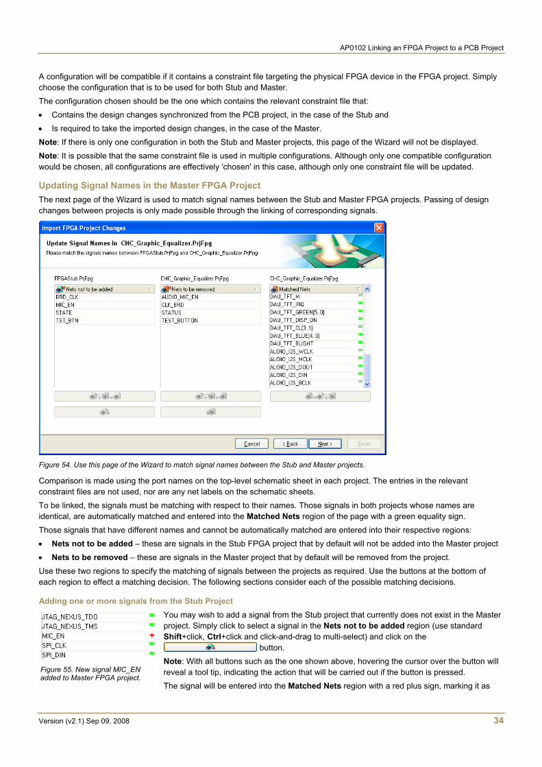
AP0102 Linking an FPGA Project to a PCB Project
Version (v2.1) Sep 09, 2008 34
A configuration will be compatible if it contains a constraint file targeting the physical FPGA device in the FPGA project. Simply choose the configuration that is to be used for both Stub and Master.
The configuration chosen should be the one which contains the relevant constraint file that:
• Contains the design changes synchronized from the PCB project, in the case of the Stub and
• Is required to take the imported design changes, in the case of the Master. Note: If there is only one configuration in both the Stub and Master projects, this page of the Wizard will not be displayed.
Note: It is possible that the same constraint file is used in multiple configurations. Although only one compatible configuration would be chosen, all configurations are effectively 'chosen' in this case, although only one constraint file will be updated.
Updating Signal Names in the Master FPGA Project The next page of the Wizard is used to match signal names between the Stub and Master FPGA projects. Passing of design changes between projects is only made possible through the linking of corresponding signals.
Figure 54. Use this page of the Wizard to match signal names between the Stub and Master projects.
Comparison is made using the port names on the top-level schematic sheet in each project. The entries in the relevant constraint files are not used, nor are any net labels on the schematic sheets.
To be linked, the signals must be matching with respect to their names. Those signals in both projects whose names are identical, are automatically matched and entered into the Matched Nets region of the page with a green equality sign.
Those signals that have different names and cannot be automatically matched are entered into their respective regions: • Nets not to be added – these are signals in the Stub FPGA project that by default will not be added into the Master project
• Nets to be removed – these are signals in the Master project that by default will be removed from the project.
Use these two regions to specify the matching of signals between the projects as required. Use the buttons at the bottom of each region to effect a matching decision. The following sections consider each of the possible matching decisions.
Adding one or more signals from the Stub Project You may wish to add a signal from the Stub project that currently does not exist in the Master project. Simply click to select a signal in the Nets not to be added region (use standard Shift+click, Ctrl+click and click-and-drag to multi-select) and click on the
button. Note: With all buttons such as the one shown above, hovering the cursor over the button will reveal a tool tip, indicating the action that will be carried out if the button is pressed. The signal will be entered into the Matched Nets region with a red plus sign, marking it as
Figure 55. New signal MIC_EN added to Master FPGA project.
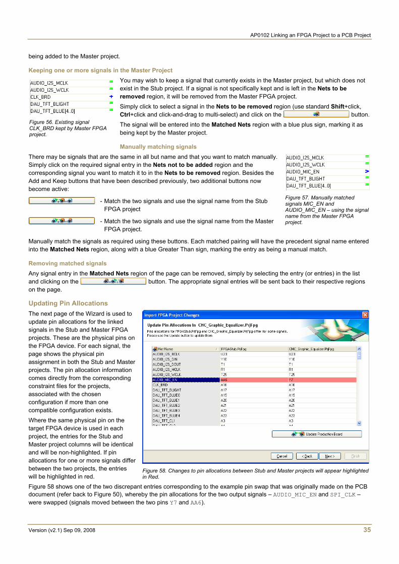
AP0102 Linking an FPGA Project to a PCB Project
Version (v2.1) Sep 09, 2008 35
being added to the Master project.
Keeping one or more signals in the Master Project You may wish to keep a signal that currently exists in the Master project, but which does not exist in the Stub project. If a signal is not specifically kept and is left in the Nets to be removed region, it will be removed from the Master FPGA project.
Simply click to select a signal in the Nets to be removed region (use standard Shift+click, Ctrl+click and click-and-drag to multi-select) and click on the button.
The signal will be entered into the Matched Nets region with a blue plus sign, marking it as being kept by the Master project.
Manually matching signals There may be signals that are the same in all but name and that you want to match manually. Simply click on the required signal entry in the Nets not to be added region and the corresponding signal you want to match it to in the Nets to be removed region. Besides the Add and Keep buttons that have been described previously, two additional buttons now become active:
- Match the two signals and use the signal name from the Stub FPGA project
- Match the two signals and use the signal name from the Master FPGA project.
Manually match the signals as required using these buttons. Each matched pairing will have the precedent signal name entered into the Matched Nets region, along with a blue Greater Than sign, marking the entry as being a manual match.
Removing matched signals Any signal entry in the Matched Nets region of the page can be removed, simply by selecting the entry (or entries) in the list and clicking on the button. The appropriate signal entries will be sent back to their respective regions on the page.
Updating Pin Allocations The next page of the Wizard is used to update pin allocations for the linked signals in the Stub and Master FPGA projects. These are the physical pins on the FPGA device. For each signal, the page shows the physical pin assignment in both the Stub and Master projects. The pin allocation information comes directly from the corresponding constraint files for the projects, associated with the chosen configuration if more than one compatible configuration exists.
Where the same physical pin on the target FPGA device is used in each project, the entries for the Stub and Master project columns will be identical and will be non-highlighted. If pin allocations for one or more signals differ between the two projects, the entries will be highlighted in red.
Figure 58 shows one of the two discrepant entries corresponding to the example pin swap that was originally made on the PCB document (refer back to Figure 50), whereby the pin allocations for the two output signals – AUDIO_MIC_EN and SPI_CLK – were swapped (signals moved between the two pins Y7 and AA6).
Figure 56. Existing signal CLK_BRD kept by Master FPGA project.
Figure 57. Manually matched signals MIC_EN and AUDIO_MIC_EN – using the signal name from the Master FPGA project.
Figure 58. Changes to pin allocations between Stub and Master projects will appear highlighted in Red.
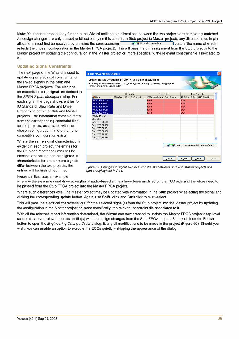
AP0102 Linking an FPGA Project to a PCB Project
Version (v2.1) Sep 09, 2008 36
Note: You cannot proceed any further in the Wizard until the pin allocations between the two projects are completely matched. As design changes are only passed unidirectionally (in this case from Stub project to Master project), any discrepancies in pin allocations must first be resolved by pressing the corresponding button (the name of which reflects the chosen configuration in the Master FPGA project). This will pass the pin assignment from the Stub project into the Master project by updating the configuration in the Master project or, more specifically, the relevant constraint file associated to it.
Updating Signal Constraints The next page of the Wizard is used to update signal electrical constraints for the linked signals in the Stub and Master FPGA projects. The electrical characteristics for a signal are defined in the FPGA Signal Manager dialog. For each signal, the page shows entries for IO Standard, Slew Rate and Drive Strength, in both the Stub and Master projects. The information comes directly from the corresponding constraint files for the projects, associated with the chosen configuration if more than one compatible configuration exists.
Where the same signal characteristic is evident in each project, the entries for the Stub and Master columns will be identical and will be non-highlighted. If characteristics for one or more signals differ between the two projects, the entries will be highlighted in red.
Figure 59 illustrates an example whereby the slew rates and drive strengths of audio-based signals have been modified on the PCB side and therefore need to be passed from the Stub FPGA project into the Master FPGA project.
Where such differences exist, the Master project may be updated with information in the Stub project by selecting the signal and clicking the corresponding update button. Again, use Shift+click and Ctrl+click to multi-select.
This will pass the electrical characteristic(s) for the selected signal(s) from the Stub project into the Master project by updating the configuration in the Master project or, more specifically, the relevant constraint file associated to it.
With all the relevant import information determined, the Wizard can now proceed to update the Master FPGA project’s top-level schematic and/or relevant constraint file(s) with the design changes from the Stub FPGA project. Simply click on the Finish button to open the Engineering Change Order dialog, listing all modifications to be made in the project (Figure 60). Should you wish, you can enable an option to execute the ECOs quietly – skipping the appearance of the dialog.
Figure 59. Changes to signal electrical constraints between Stub and Master projects will appear highlighted in Red.
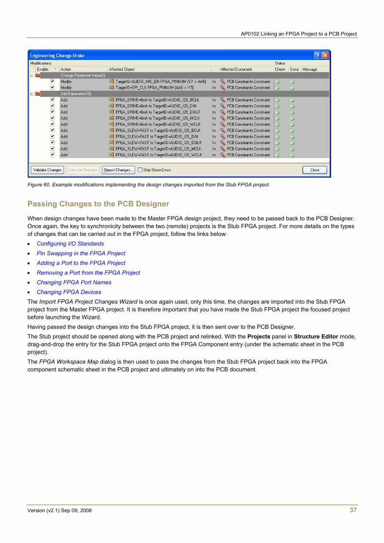
AP0102 Linking an FPGA Project to a PCB Project
Version (v2.1) Sep 09, 2008 37
Figure 60. Example modifications implementing the design changes imported from the Stub FPGA project.
Passing Changes to the PCB Designer
When design changes have been made to the Master FPGA design project, they need to be passed back to the PCB Designer. Once again, the key to synchronicity between the two (remote) projects is the Stub FPGA project. For more details on the types of changes that can be carried out in the FPGA project, follow the links below:
• Configuring I/O Standards
• Pin Swapping in the FPGA Project
• Adding a Port to the FPGA Project
• Removing a Port from the FPGA Project
• Changing FPGA Port Names
• Changing FPGA Devices The Import FPGA Project Changes Wizard is once again used, only this time, the changes are imported into the Stub FPGA project from the Master FPGA project. It is therefore important that you have made the Stub FPGA project the focused project before launching the Wizard.
Having passed the design changes into the Stub FPGA project, it is then sent over to the PCB Designer. The Stub project should be opened along with the PCB project and relinked. With the Projects panel in Structure Editor mode, drag-and-drop the entry for the Stub FPGA project onto the FPGA Component entry (under the schematic sheet in the PCB project).
The FPGA Workspace Map dialog is then used to pass the changes from the Stub FPGA project back into the FPGA component schematic sheet in the PCB project and ultimately on into the PCB document.

AP0102 Linking an FPGA Project to a PCB Project
Version (v2.1) Sep 09, 2008 38
Revision History
Date Version No. Revision
20-Jan-2004 1.0 New product release
01-Jul-2005 1.1 Updated for Altium Designer SP4
28-Feb-2008 2.0 Updated for Altium Designer Summer 08
09-Sep-2008 2.1 Fully updated in line with current software functionality.
02-Aug-2011 - Updated template.
Software, hardware, documentation and related materials:
Copyright © 2011 Altium Limited.
All rights reserved. You are permitted to print this document provided that (1) the use of such is for personal use only and will not be copied or posted on any network computer or broadcast in any media, and (2) no modifications of the document is made. Unauthorized duplication, in whole or part, of this document by any means, mechanical or electronic, including translation into another language, except for brief excerpts in published reviews, is prohibited without the express written permission of Altium Limited. Unauthorized duplication of this work may also be prohibited by local statute. Violators may be subject to both criminal and civil penalties, including fines and/or imprisonment.
Altium, Altium Designer, Board Insight, DXP, Innovation Station, LiveDesign, NanoBoard, NanoTalk, OpenBus, P-CAD, SimCode, Situs, TASKING, and Topological Autorouting and their respective logos are trademarks or registered trademarks of Altium Limited or its subsidiaries. All other registered or unregistered trademarks referenced herein are the property of their respective owners and no trademark rights to the same are claimed.