Lecture-42 & 43 EE5325 Power Management Integrated Circuits
17
11/9/2018 1 Lecture-42 & 43 EE5325 Power Management Integrated Circuits Dr. Qadeer Ahmad Khan Integrated Circuits and Systems Group Department of Electrical Engineering IIT Madras 1 EE5325 Power Management Integrated Circuits Integrated Circuits and Systems Group, Department of EE, IIT Madras Limitations of Analog Controller The compensation network is usually designed with RC and for 1MHz or lower frequencies, the value of capacitor is large and kept off-chip The discrete nature of compensator makes it difficult to track any variation in loop parameters (L, C, R) Does not provide reconfigurability Ref: Optimizing Low-Power DC/DC Designs – External versus Internal Compensation,Michael Day, Texas Instrumets 2 EE5325 Power Management Integrated Circuits Integrated Circuits and Systems Group, Department of EE, IIT Madras
Transcript of Lecture-42 & 43 EE5325 Power Management Integrated Circuits

11/9/2018
1
Lecture-42 & 43
EE5325 Power Management Integrated Circuits
Dr. Qadeer Ahmad Khan
Integrated Circuits and Systems Group
Department of Electrical Engineering
IIT Madras
1EE5325 Power Management Integrated Circuits Integrated Circuits and Systems Group, Department of EE, IIT Madras
Limitations of Analog Controller
The compensation network is usually designed with RC and for 1MHz or lower frequencies, the value of capacitor is large and kept off-chip
The discrete nature of compensator makes it difficult to track any variation in loop parameters (L, C, R)
Does not provide reconfigurability
Ref: Optimizing Low-Power DC/DC Designs – External versus
Internal Compensation,Michael Day, Texas Instrumets
2EE5325 Power Management Integrated Circuits Integrated Circuits and Systems Group, Department of EE, IIT Madras

11/9/2018
2
Digital Control of DC-DC Converters
Why Digital Control?
Unlike the analog control, digital control provides the flexibility of tuning filter coefficients and can be easily reconfigured
Fully integrated solution - no off chip compensation
The loop can be designed to adapt any changes in both on-chip and off-chip components due to aging, process, temperature or vendor selection
Easily scalable with the process-blocks can synthesized
4EE5325 Power Management Integrated Circuits Integrated Circuits and Systems Group, Department of EE, IIT Madras

11/9/2018
3
Digitally Controlled DC-DC Converter
The error voltage is digitized and processed in digital compensator (digital filter)
The analog PWM is replaced with digital PWM
+
-
+
VPWM
Dc<m:0> De<n:0> Vref
Vout
Verr PID
Digital
PWM
Digital
CompensatorAnalog to Digital
Converter
Gate
Driver
CONTROLLER
Rload
Iload
Vin
C
L Vout
5EE5325 Power Management Integrated Circuits Integrated Circuits and Systems Group, Department of EE, IIT Madras
Constraints on ADC
The resolution of ADC depends upon the regulation specification
Vout = 1V, if regulation specification is 0.1% ΔV = 1mV– Requires a 10Bit ADC
Conversion rate depends upon PWM switching Frequency, ideally it should be less than one clock period– A slow ADC might interfere with the loop dynamic and degrade
phase margin
6EE5325 Power Management Integrated Circuits Integrated Circuits and Systems Group, Department of EE, IIT Madras

11/9/2018
4
Analog-to-Digital Converter (ADC) Architectures
Windowed ADC
Designing a high resolution ADC is complex and power consuming
Since the output is a fixed voltage and need to be regulated around reference voltage, a windowed ADC can be used
This reduces the no. of bins without degrading the regulation
The range of ADC is restricted to small input
– If LSB = 1mV then ADC can be designed to resolve few LSBs
– For example, window size = 6mV requires only levels means 3-bit ADC will give the accuracy of 10-bit
8EE5325 Power Management Integrated Circuits Integrated Circuits and Systems Group, Department of EE, IIT Madras
11/9/2018
5
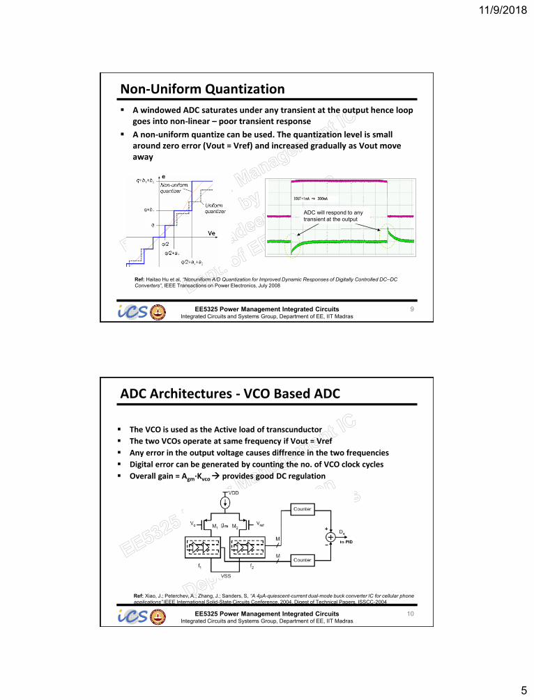
Non-Uniform Quantization
A windowed ADC saturates under any transient at the output hence loop goes into non-linear – poor transient response
A non-uniform quantize can be used. The quantization level is small around zero error (Vout = Vref) and increased gradually as Vout move away
ADC will respond to any
transient at the output
Ref: Haitao Hu et al, “Nonuniform A/D Quantization for Improved Dynamic Responses of Digitally Controlled DC–DC
Converters”, IEEE Transactions on Power Electronics, July 2008
9EE5325 Power Management Integrated Circuits Integrated Circuits and Systems Group, Department of EE, IIT Madras
ADC Architectures - VCO Based ADC
The VCO is used as the Active load of transcunductor
The two VCOs operate at same frequency if Vout = Vref
Any error in the output voltage causes diffrence in the two frequencies
Digital error can be generated by counting the no. of VCO clock cycles
Overall gain = Agm·Kvco provides good DC regulation
Ref: Xiao, J.; Peterchev, A.; Zhang, J.; Sanders, S, “A 4μA-quiescent-current dual-mode buck converter IC for cellular phone
applications” IEEE International Solid-State Circuits Conference, 2004. Digest of Technical Papers. ISSCC-2004
10EE5325 Power Management Integrated Circuits Integrated Circuits and Systems Group, Department of EE, IIT Madras

11/9/2018
6
Delay Line Based ADC
Vref and Vout is converted into delay and phase difference is measured Uses single delay line and Vref is sampled and calibrated in order to cancel
any variation due to PVT Poor PSRR
– Since Vref and Vout are sampled at different instance any noise in the VDD may introduce error
Ref: Patella, B.J.; Prodic, A.; Zirger, A.; Maksimovic, D., “High-frequency digital PWM controller IC for DC-DC converters”,
IEEE Transactions on Power Electronics, Volume 18, Issue 1, Jan 2003
11EE5325 Power Management Integrated Circuits Integrated Circuits and Systems Group, Department of EE, IIT Madras
Improved Delay Line Based ADC
Vref and Vout use separate delay lines and sampled at same instance good PSSR
Uses differential input pairs to bias the delay lines in order to reduce the dependency on Vref VCDL characteristic does not change across different Vout
Ref: Lukic, Z.; Rahman, N.; Prodic, A., “Multibit Sigma-Delta PWM Digital Controller IC for DC–DC Converters Operating at
Switching Frequencies Beyond 10 MHz”, ,IEEE Transactions on Power Electronics, Sept. 2007
12EE5325 Power Management Integrated Circuits Integrated Circuits and Systems Group, Department of EE, IIT Madras

11/9/2018
7
Digital Pulse-Width Modulator (DPWM) Architectures
DPWM Resolution - Limit Cycle Oscillation
The resolution of DPWM should be higher than the resolution of ADC to avoid limit cycle oscillation
– 1 LSB change in duty cycle should cause lesser change in Vout than 1 LSB of ADC
If DPWM resolution is less, the ADC does not find any zero-error bin
The output oscillates around the regulated dc voltage.
– The amplitude of oscillation depends upon DPWM resolution
Vout with Lower DPWM resolution Vout with Higher DPWM resolution
Peterchev, A.V.; Sanders, S.R., “Quantization resolution and limit cycling in digitally controlled PWM converters”, IEEE
Transactions on Power Electronics, Volume 18, Issue 1, Jan 2003
14EE5325 Power Management Integrated Circuits Integrated Circuits and Systems Group, Department of EE, IIT Madras

11/9/2018
8
Counter Based DPWM
Uses a high frequency clock to Count the PWM clock period
The Counter output is compared with the error code and duty cycle is reset when counter output crosses the error code
The step size of duty cycle is given by
Difficult to realize as max frequency is limited by the technology
– If ADC LSB = 1mV, then 1 LSB of DPWM should cause less than 1mV change in Vout to avoid limit cycling if DC-DC is switching at 1MHz then it may require high frequency clock of few GHz
2kDPWM -1
Error Code
Tsw=1/fsw
Ton Toff
Tclk=1/fclk
PWM
SET
RESET
clk
sw
f
fD
15EE5325 Power Management Integrated Circuits Integrated Circuits and Systems Group, Department of EE, IIT Madras
DLL Based DPWM
Does not require high frequency clock relatively low power consumption
Use multiple phase to reset the duty cycle
The duty cycle step size is defined by ; m is the no. of phasesmD
1
Tsw=1/fsw
Ton Toff
PWM
Ф0
Ф1
Фm-1
Фm-2
Фm-3
Фm-4
Фm-5
Фm-6
SET
RESET
ΔT
16EE5325 Power Management Integrated Circuits Integrated Circuits and Systems Group, Department of EE, IIT Madras

11/9/2018
9
Increasing the resolution of DPWM
The resolution of counter based and delay in DLL based DPWM is limited by the technology or power consumption
Dithering is generally used to increase the resolution
Causes low frequency ripple at the output voltage depends on resolution
Fixed Ripple Frequency Dither Variable Ripple Frequency Dither (reduce ripple)
Dc1=0.1, Dc2=0.2
Dc1+1/LSB=(3*Dc1+1*Dc2)4
= (0.3+0.2)/4 = 0.125
ΔD=0.125-0.1 = 0.025
4x resolution
17EE5325 Power Management Integrated Circuits Integrated Circuits and Systems Group, Department of EE, IIT Madras
Delta-Sigma Based PWM Control
The low frequency dither tones is randomized by using delta-sigma modulator
Relatively slower as compared to standard dithering
+
-
+
VPWM
M-Bits De<n:0> Vref
Vout
Verr
PID
Digital
PWM
Digital
Compensator
Analog to Digital
Converter
Gate
Driver
CONTROLLER
Rload
Iload
Vin
C
L
ΔΣ
N-Bits
(LSB)
M-N Bits
(MSB)
1-Bit Random
Sequence
Vout
PWM
Delta-Sigma
Modulator
18EE5325 Power Management Integrated Circuits Integrated Circuits and Systems Group, Department of EE, IIT Madras

11/9/2018
10
Adaptive Compensation
Need for Adaptive Compensation
The control loop can made self compensated by automatic tuning of filter parameters
Provides robustness over wide variation of operating condition and component values Plug and Play
Gain, Phase Margin and values of internal and external components (L, C, Ron, Resr etc.) can be monitored continuously
20EE5325 Power Management Integrated Circuits Integrated Circuits and Systems Group, Department of EE, IIT Madras

11/9/2018
11
Tuning Methods
Based on Middlebrooke’s injection technique Middlebrooke’s Technique: Does not require to break the loop Crossover frequency can be determined by the injection signal frequency
at which loop gain becomes unity
Loop TF is given by
Ref: J. Morroni, R. Zane, D. Maksimovic, “An Online Phase Margin Monitor for Digitally Controlled Switched Mode Power
Supplies” Power Electronics Specialist Conference, 2008
Middlebrooke’s Method
21EE5325 Power Management Integrated Circuits Integrated Circuits and Systems Group, Department of EE, IIT Madras
Middlebrooke’s Method (Contd.)
The injected signal is variable frequency square wave therefore requires narrow BPF to get rid of higher harmonics
Peak Detector is used to determine the amplitude of Vx and Vy and compared
Phase Margin is determined as the phase difference between two signal
Detection of crossover frequency Detection of Phase Margin
Zero crossing detector
22EE5325 Power Management Integrated Circuits Integrated Circuits and Systems Group, Department of EE, IIT Madras

11/9/2018
12
Correlation Based Method
Uses PRBS generator to determine the impulse response and transfer function is determined by DFT
PRBS is shaped in pre-emphasis filter which boost the output above the noise floor of ADC in order to reduce the quantization effect
Cross correlation to obtain the impulse response is computed using Fast Walsh-Hadamard Transform (FWHT)
23EE5325 Power Management Integrated Circuits Integrated Circuits and Systems Group, Department of EE, IIT Madras
Correlation Based Method (Contd.)
PRBS is shaped in pre-emphasis filter which boost the output above the noise floor of ADC in order to reduce the quantization effect
Cross correlation to obtain the impulse response is computed using Fast Walsh-Hadamard Transform (FWHT)
M. Shirazi, J. Morroni, A. Dolgov, R. Zane, D. Maksimovic,” Integration of Frequency Response Measurement Capabilities in Digital
Controllers for DC-DC Converters”, IEEE Transaction on Power Electronics, 2008
24EE5325 Power Management Integrated Circuits Integrated Circuits and Systems Group, Department of EE, IIT Madras

11/9/2018
13
Limit Cycling Oscillation Based Tuning
The method enforces the limit cycle oscillations by reducing the resolution of DPWM under test mode
The oscillations at the output are analyzed to measure the loop parameters
The loop is turned into Integral to measure the oscillations
Z. Zhao, A. Prodic, “Limit-Cycle Oscillation Based Auto-Tuning System for Digitally Controlled DC-DC Power
Supplies”, IEEE Transaction on Power Electronics, 2007
25EE5325 Power Management Integrated Circuits Integrated Circuits and Systems Group, Department of EE, IIT Madras
Limitations with Digital Control
ADC is not a big constraint for DC-DC as there are numerous architectures available which can easily meet the requirement
Designing high resolution of DPWM is a challenging task for faster loop bandwidth as dithering slows down the loop
All the Adaptive Compensation techniques reported in papers require test signal during normal operation normal operation is disturbed or amplitude of test signal should be low enough reduced accuracy
The existing adaptive compensation techniques can’t be used in dynamic supply applications such as RF Power Amplifier and Class-H audio where supply is modulated with RF envelope or audio signal test signal might fall into the signal frequency
26EE5325 Power Management Integrated Circuits Integrated Circuits and Systems Group, Department of EE, IIT Madras

11/9/2018
14
Simplified Tuning Techniques
Measurement Method
The technique works in two steps
In test mode during the startup, a short pulse is applied at the power stage and oscillations are measured ωo is determined
Once the ωo is known, duty cycle is modulated with a sine wave of frequency ωo and amplitude is measured at the output gives Qo
28EE5325 Power Management Integrated Circuits Integrated Circuits and Systems Group, Department of EE, IIT Madras

11/9/2018
15
)()()(,.. sHsGVm
VinsTFTLoop LCc
2
0
0
02
2
0)(
wsQ
ws
wsH LC
s
wsQ
ws
GsGif oc
2
0
0
02
)(
sG
Vm
VinsTFTLoop
1)(,.. 0
Loop becomes a single pole system
loss
load
load
loss
load
loss
CRR
L
R
R
LCQandR
R
LCw
1
11
00
loss
loadload
load
CRLCIQand
LCIw
Rconditionloadnounder
1)0(
1)0(
)(
00
Vm
Vin)(sGc
Iload
C
L Vout
Rload
Rloss
)(sH LC
PWM Compensator
Power Stage
Which we already measured from the test setup
Simplified model of the DC-DC Converter
Measurement Method
29EE5325 Power Management Integrated Circuits Integrated Circuits and Systems Group, Department of EE, IIT Madras
Estimation of Rloss and Rload
After ωo and Qo are estimated, the DC-DC is switched to normal operation mode and other parameters are calculated
For a buck converter, ideally, the output voltage is given by:
But this equation never satisfies due to losses in the power stage duty cycle is always higher than the required to compensate for the losses. The voltage loss can be calculated as:
Ideal Vout – Actual Vout
If Iload is known from the current sensing, Rloss and Rload can be calculated as:
inout VDV
outinloss VVDV
load
outload
load
lossloss
I
VRand
I
VR
30EE5325 Power Management Integrated Circuits Integrated Circuits and Systems Group, Department of EE, IIT Madras

11/9/2018
16
Estimation of L and CThe voltage across the inductor is given by:
The inductor value can be estimated as:
Where m1 and m2 are the charging discharging
Slope of the inductor current
Capacitor can be calculated as:
dT
dILV L
L
m1 m2
S1ON S2ON
IL
21 m
VVLor
m
VL outinout
)0(
12
0
loadIwLC
31EE5325 Power Management Integrated Circuits Integrated Circuits and Systems Group, Department of EE, IIT Madras
Adaptive Compensation
Now all the values could be fed in the following equation and used to calculate the location of compensation zeroes in the real time.
The method tracks the location of complex poles in the real time under any changes due to ESR, Temperature, Process etc without disturbing the normal operation of the DC-DC Converter
The measured data can also be used to estimate other parameters like efficiency and ON resistances of Power FETs for maintenance purpose
loss
load
load
loss
load
loss
CRR
L
R
R
LCQandR
R
LCw
1
11
00
32EE5325 Power Management Integrated Circuits Integrated Circuits and Systems Group, Department of EE, IIT Madras

11/9/2018
17
Increasing the Resolution of Digital PWM
Technique for increasing the resolution of PWM
Since Analog PWM provides infinite resolution so the simplest solution would be to use analog PWM instead of Digital
The Digital Control Word from Compensator output is converter to Analog using high resolution D/A Converter
+
-
+
VPWM
Dc<m:0> De<n:0>
Vref
Vout
Verr PID
Digital
CompensatorAnalog to Digital
Converter
Gate
Driver
CONTROLLER
Rload
Iload
Vin
C
L
High
Resolution
DAC
Analog
PWM
Vc
DAC
Vout
Modified PWM Controller for High Resolution
34EE5325 Power Management Integrated Circuits Integrated Circuits and Systems Group, Department of EE, IIT Madras