Lecture 1 Combinational Logic Design & Flip Flop 2007/09/07 Prof. C.M. Kyung.
25
Lecture 1 Combinational Logic Design & Flip Flop 2007/09/07 Prof. C.M. Kyung
-
Upload
hester-williams -
Category
Documents
-
view
217 -
download
3
Transcript of Lecture 1 Combinational Logic Design & Flip Flop 2007/09/07 Prof. C.M. Kyung.

Lecture 1 Combinational Logic Design & Flip Flop
2007/09/07
Prof. C.M. Kyung
2/25
Combinational Logic Design & Flip Flop
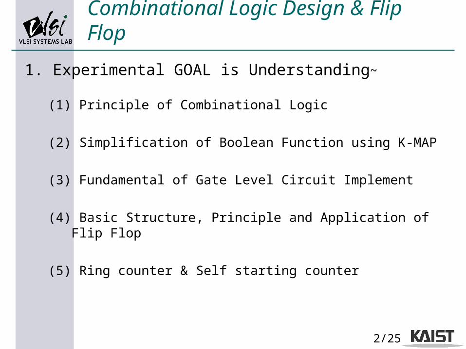
1. Experimental GOAL is Understanding~
(1) Principle of Combinational Logic
(2) Simplification of Boolean Function using K-MAP
(3) Fundamental of Gate Level Circuit Implement
(4) Basic Structure, Principle and Application of Flip Flop
(5) Ring counter & Self starting counter

3/25
Combinational Logic Design & Flip Flop
2. Combinational Logic Implement Step
(1) Understanding about Specification
(2) Truth Table & K-Map
(3) Find Prime Implicant from the K-Map & Simplification
(4) Gate Level Circuit Implement
(5) Verification

4/25
Combinational Logic Design & Flip Flop
3. Combinational Logic Implement Step - Example (2’s complement viewer)
(1) Truth table

5/25
Combinational Logic Design & Flip Flop
(2) K-Map
(3) Boolean Algebra

6/25
Combinational Logic Design & Flip Flop
(3) Gate level circuit Implement

7/25
Combinational Logic Design & Flip Flop
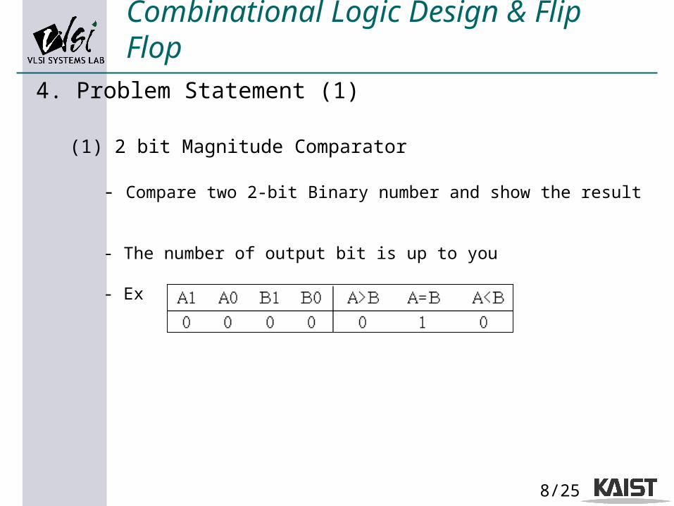
4. Problem Statement (1)
(1) 2 bit Magnitude Comparator
(2) BCD-to-7 segment display code converter
8/25
Combinational Logic Design & Flip Flop
4. Problem Statement (1)
(1) 2 bit Magnitude Comparator
- Compare two 2-bit Binary number and show the result
- The number of output bit is up to you
- Ex

9/25
Combinational Logic Design & Flip Flop
4. Problem Statement (1)
(2) BCD-to-7 segment display code converter
- Input 4-bit number should be displayed in 7 segment
- Only the number from 0 to 9 is valuable

10/25
Combinational Logic Design & Flip Flop
- You can use anode or cathode type

11/25
Combinational Logic Design & Flip Flop
5. Flip – Flop
(1) S - R Latch
- Input S (set) = High -->> Output Q = High- Input R (reset) = High -->> Output Q = Low

12/25
Combinational Logic Design & Flip Flop
(2) S - R Latch with Clock
- Latch = Output changes when input changes- Flip Flop = Output changes when Clock changes

13/25
Combinational Logic Design & Flip Flop
(3) D – Flip Flop
- Posedge detection (Dual D - FF)

14/25
Combinational Logic Design & Flip Flop
(3) D – Flip Flop
- Posedge detection (Dual D - FF)

15/25
Combinational Logic Design & Flip Flop
(4) J-K Flip Flop

16/25
Combinational Logic Design & Flip Flop
(4) J-K Flip Flop
- Falling Edge Detection

17/25
Combinational Logic Design & Flip Flop
(5) T - Flip Flop
- Assign J = K in J-K Flip Flop

18/25
Combinational Logic Design & Flip Flop
6. Counter
(1) Asynchronous Counter
- Each Flip Flop controlled by Q’ of Former FF

19/25
Combinational Logic Design & Flip Flop
6. Counter
(2) Synchronous Counter
- Every Flip Flop controlled by same Clock signal

20/25
Combinational Logic Design & Flip Flop
7. Problem Statement (2)
(1) Asynchronous Down Counter
(2) Synchronous Up Counter

21/25
Combinational Logic Design & Flip Flop
7. Problem Statement (2)
(1) Asynchronous 3-bit Ring Down Counter
- Each Flip Flop controlled by Q’ of Former FF
- Accumulation of Flip Flop Delay in Each stage
- Using J-K Flip Flop
- Sequence : 7-6-5-4-3-2-1-0-7-6-5-4-3-2-1-0-7-6…

22/25
Combinational Logic Design & Flip Flop
7. Problem Statement (2)
(2) Synchronous 3-bit Self starting Counter
- Every Flip Flop controlled by same Clock signal
- Each stage has 1 FF delay
- Using D Flip Flop
- Sequence : 1-3-4-6-7-1-3-4-6-7-1-3-4-6-7-…
- If the initial value is 0 or 2 or 5, How can you handle it ?

23/25
Combinational Logic Design & Flip Flop
8. Problem Statement (3)
(1) Combine BCD-to-7 segment decoder & statement (2)
- Result of counter must be expressed on 7-segment display
- Counter output should be input of the Decoder
- You can use LSB 3bit of the decoder

24/25
Combinational Logic Design & Flip Flop
9. Experiment Requirements (1) Equipment
- Breadboard- Multimeter- DC Power Supply
(2) Component- Switch - 7-segment (cathode & anode)
(3) TTL IC’s- 7400 (2 input NAND gate)- 7404 (Inverter)- 7408 (2 input AND gate)- 7410 (3 input NAND gate)- 74LS73 ( Dual J-K flip-flop )- 74LS74 ( Dual D-Type flip-flop )
25/25
Combinational Logic Design & Flip Flop
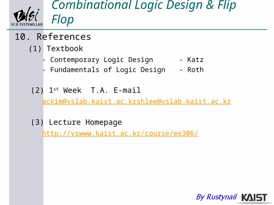
10. References (1) Textbook
- Contemporary Logic Design - Katz
- Fundamentals of Logic Design - Roth
(2) 1st Week T.A. E-mail [email protected]@vslab.kaist.ac.kr
(3) Lecture Homepage http://vswww.kaist.ac.kr/course/ee306/