LC2MOS Complete 14-Bit, Sampling ADCs AD7871/AD7872
24
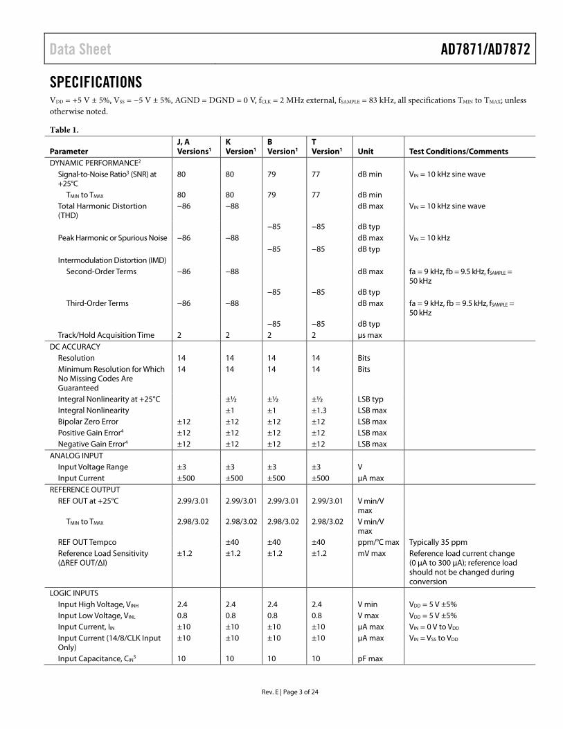
LC 2 MOS Complete 14-Bit, Sampling ADCs Data Sheet AD7871/AD7872 FEATURES Complete monolithic 14-bit ADC Twos complement coding Parallel, byte, and serial digital interface 80 dB SNR at 10 kHz input frequency 57 ns data access time Low power: 50 mW typ 83 kSPS throughput rate APPLICATIONS Digital signal processing High speed modems Speech recognition and synthesis Spectrum analysis DSP servo control GENERAL DESCRIPTION The AD7871/AD7872 are fast, complete, 14-bit analog-to- digital converters (ADC). They consist of a track-and-hold amplifier, successive approximation ADC, 3 V buried Zener reference, and versatile interface logic. The ADC features a self- contained, laser trimmed internal clock, so no external clock timing components are required. The on-chip clock may be overridden to synchronize ADC operation to the digital system for minimum noise. The AD7871 offers a choice of three data output formats: a single, parallel, 14-bit word; two 8-bit bytes or a 14-bit serial data stream. The AD7872 is a serial output device only. The two parts are capable of interfacing to all modern microprocessors and digital signal processors. The AD7871/AD7872 operate from ±5 V power supplies, accept bipolar input signals of ±3 V and can convert full power signals up to 41.5 kHz. In addition to the traditional dc accuracy specifications, the AD7871/AD7872 are also fully specified for dynamic performance parameters including distortion and signal-to- noise ratio. FUNCTIONAL BLOCK DIAGRAMS Figure 1. Figure 2. Both devices are fabricated in Analog Devices, Inc., LC 2 MOS mixed technology process. The AD7871 is available in 28-pin PDIP, PLCC, and CERDIP packages. The AD7872 is available in a 16-pin PDIP, CERDIP, and SOIC packages. PRODUCT HIGHLIGHTS 1. Complete 14-Bit ADC on a Chip. 2. Dynamic Specifications for DSP Users. 3. Low Power. REF OUT 14-BIT DAC PARALLEL AND SERIAL INTERFACE AD7871 CONTROL LOGIC CLOCK 3V REFERENCE SAR + COUNTER COMP TRACK- AND-HOLD V DD V SS DGND DB13 DB0 CS RD BUSY/INT AGND CLK CONVST 14/8/CLK 22 5 28 1 2 3 4 6 20 14 27 25 C REF 23 V IN 26 21 R R 12889-001 REF OUT 14-BIT DAC SERIAL INTERFACE AD7872 CONTROL LOGIC CLOCK 3V REFERENCE SAR + COUNTER COMP TRACK- AND-HOLD AGND CLK CONVST CONTROL 12 3 1 2 SSTRB 4 SCLK 5 SDATA 6 DGND 8 V SS 15 13 C REF 11 V IN 14 V DD 9 V DD 16 R R 12889-002 Rev. E Document Feedback Information furnished by Analog Devices is believed to be accurate and reliable. However, no responsibility is assumed by Analog Devices for its use, nor for any infringements of patents or other rights of third parties that may result from its use. Specifications subject to change without notice. No license is granted by implication or otherwise under any patent or patent rights of Analog Devices. Trademarks and registered trademarks are the property of their respective owners. One Technology Way, P.O. Box 9106, Norwood, MA 02062-9106, U.S.A. Tel: 781.329.4700 ©2015 Analog Devices, Inc. All rights reserved. Technical Support www.analog.com
-
Upload
phunghuong -
Category
Documents
-
view
216 -
download
0
Transcript of LC2MOS Complete 14-Bit, Sampling ADCs AD7871/AD7872
LC2MOS Complete 14-Bit, Sampling ADCs
Data Sheet AD7871/AD7872
FEATURES Complete monolithic 14-bit ADC Twos complement coding Parallel, byte, and serial digital interface 80 dB SNR at 10 kHz input frequency 57 ns data access time Low power: 50 mW typ 83 kSPS throughput rate
APPLICATIONS Digital signal processing High speed modems Speech recognition and synthesis Spectrum analysis DSP servo control
GENERAL DESCRIPTION The AD7871/AD7872 are fast, complete, 14-bit analog-to-digital converters (ADC). They consist of a track-and-hold amplifier, successive approximation ADC, 3 V buried Zener reference, and versatile interface logic. The ADC features a self-contained, laser trimmed internal clock, so no external clock timing components are required. The on-chip clock may be overridden to synchronize ADC operation to the digital system for minimum noise.
The AD7871 offers a choice of three data output formats: a single, parallel, 14-bit word; two 8-bit bytes or a 14-bit serial data stream. The AD7872 is a serial output device only. The two parts are capable of interfacing to all modern microprocessors and digital signal processors.
The AD7871/AD7872 operate from ±5 V power supplies, accept bipolar input signals of ±3 V and can convert full power signals up to 41.5 kHz.
In addition to the traditional dc accuracy specifications, the AD7871/AD7872 are also fully specified for dynamic performance parameters including distortion and signal-to-noise ratio.
FUNCTIONAL BLOCK DIAGRAMS
Figure 1.
Figure 2.
Both devices are fabricated in Analog Devices, Inc., LC2MOS mixed technology process. The AD7871 is available in 28-pin PDIP, PLCC, and CERDIP packages. The AD7872 is available in a 16-pin PDIP, CERDIP, and SOIC packages.
PRODUCT HIGHLIGHTS 1. Complete 14-Bit ADC on a Chip. 2. Dynamic Specifications for DSP Users. 3. Low Power.
REF OUT
14-BITDAC
PARALLELAND SERIALINTERFACE
AD7871
CONTROLLOGIC
CLOCK
3VREFERENCE
SAR +COUNTER
COMP
TRACK-AND-HOLD
VDD
VSSDGNDDB13 DB0CS RD BUSY/INT
AGND
CLK
CONVST
14/8/CLK
22
5
28
1
2 3 4 6 20 14 27
25
CREF23
VIN26 21
R
R
1288
9-00
1
REF OUT
14-BITDAC
SERIALINTERFACE AD7872
CONTROLLOGIC
CLOCK
3VREFERENCE
SAR +COUNTER
COMP
TRACK-AND-HOLD
AGND
CLK
CONVST
CONTROL
12
3
1
2
SSTRB4
SCLK5
SDATA6
DGND8
VSS
15
13
CREF11
VIN14
VDD9
VDD16
R
R
1288
9-00
2
Rev. E Document Feedback Information furnished by Analog Devices is believed to be accurate and reliable. However, no responsibility is assumed by Analog Devices for its use, nor for any infringements of patents or other rights of third parties that may result from its use. Specifications subject to change without notice. No license is granted by implication or otherwise under any patent or patent rights of Analog Devices. Trademarks and registered trademarks are the property of their respective owners.
One Technology Way, P.O. Box 9106, Norwood, MA 02062-9106, U.S.A. Tel: 781.329.4700 ©2015 Analog Devices, Inc. All rights reserved. Technical Support www.analog.com
AD7871/AD7872 Data Sheet
TABLE OF CONTENTS Features .............................................................................................. 1 Applications ....................................................................................... 1 General Description ......................................................................... 1 Functional Block Diagrams ............................................................. 1 Product Highlights ........................................................................... 1 Revision History ............................................................................... 2 Specifications ..................................................................................... 3
Timing Characteristics ................................................................ 5 Absolute Maximum Ratings ............................................................ 6
ESD Caution .................................................................................. 6 Pin Configuration and Function Descriptions ............................. 7 Theory of Operation ........................................................................ 9
Converter Details .......................................................................... 9 Internal Reference ........................................................................ 9 Track-And-Hold Amplifier ......................................................... 9 Analog Input ................................................................................. 9 Bipolar Offset Scale Adjustment .............................................. 10 Unipolar Operation .................................................................... 10
Unipolar Offset And Full-Scale Adjustment .......................... 10 Timing and Control ................................................................... 11 Data Output Formats ................................................................. 11 Mode 1 Interface ......................................................................... 12 Mode 2 Interface ......................................................................... 13 Dynamic Specifications ............................................................. 14 Microprocessor Interface .......................................................... 15 StandAlone Operation ............................................................... 16
Application Information ................................................................ 17 Layout Hints ................................................................................ 17 Noise ............................................................................................ 17 Data Acquisition Board ............................................................. 17 Interface Connections ............................................................... 18 Power Supply Connections ....................................................... 18 Shorting Plug Options ............................................................... 18
Outline Dimensions ....................................................................... 21 Ordering Guide .......................................................................... 24
REVISION HISTORY 1/15—Rev. D to Rev. E
Updated Format .................................................................. Universal Changed T Version Minimum SNR from 79 dB to 77 dB and Changed T Version Maximum INL from ±1 LSB to ±1.3 LSB ... 3 Deleted ADSP-2100 and TMS32020/C25 (Throughout) .......... 15 Deleted DSP56000 and ADSP-2101/ADSP-2102 (Throughout) ... 16 Updated Outline Dimensions ....................................................... 21 Changes to Ordering Guide .......................................................... 24
1/97—Rev. C to Rev. D
Rev. E | Page 2 of 24
Data Sheet AD7871/AD7872
SPECIFICATIONS VDD = +5 V ± 5%, VSS = −5 V ± 5%, AGND = DGND = 0 V, fCLK = 2 MHz external, fSAMPLE = 83 kHz, all specifications TMIN to TMAX; unless otherwise noted.
Table 1.
Parameter J, A Versions1
K Version1
B Version1
T Version1 Unit Test Conditions/Comments
DYNAMIC PERFORMANCE2 Signal-to-Noise Ratio3 (SNR) at +25°C
80 80 79 77 dB min VIN = 10 kHz sine wave
TMIN to TMAX 80 80 79 77 dB min Total Harmonic Distortion (THD)
−86 −88 dB max VIN = 10 kHz sine wave
−85 −85 dB typ Peak Harmonic or Spurious Noise −86 −88 dB max VIN = 10 kHz −85 −85 dB typ Intermodulation Distortion (IMD)
Second-Order Terms −86 −88 dB max fa = 9 kHz, fb = 9.5 kHz, fSAMPLE = 50 kHz
−85 −85 dB typ Third-Order Terms −86 −88 dB max fa = 9 kHz, fb = 9.5 kHz, fSAMPLE =
50 kHz −85 −85 dB typ Track/Hold Acquisition Time 2 2 2 2 µs max
DC ACCURACY Resolution 14 14 14 14 Bits Minimum Resolution for Which No Missing Codes Are Guaranteed
14 14 14 14 Bits
Integral Nonlinearity at +25°C ±½ ±½ ±½ LSB typ Integral Nonlinearity ±1 ±1 ±1.3 LSB max Bipolar Zero Error ±12 ±12 ±12 ±12 LSB max Positive Gain Error4 ±12 ±12 ±12 ±12 LSB max Negative Gain Error4 ±12 ±12 ±12 ±12 LSB max
ANALOG INPUT Input Voltage Range ±3 ±3 ±3 ±3 V Input Current ±500 ±500 ±500 ±500 µA max
REFERENCE OUTPUT REF OUT at +25°C 2.99/3.01 2.99/3.01 2.99/3.01 2.99/3.01 V min/V
max
TMIN to TMAX 2.98/3.02 2.98/3.02 2.98/3.02 2.98/3.02 V min/V max
REF OUT Tempco ±40 ±40 ±40 ppm/°C max Typically 35 ppm Reference Load Sensitivity (ΔREF OUT/ΔI)
±1.2 ±1.2 ±1.2 ±1.2 mV max Reference load current change (0 µA to 300 µA); reference load should not be changed during conversion
LOGIC INPUTS Input High Voltage, VINH 2.4 2.4 2.4 2.4 V min VDD = 5 V ±5% Input Low Voltage, VINL 0.8 0.8 0.8 0.8 V max VDD = 5 V ±5% Input Current, IIN ±10 ±10 ±10 ±10 µA max VIN = 0 V to VDD Input Current (14/8/CLK Input Only)
±10 ±10 ±10 ±10 µA max VIN = VSS to VDD
Input Capacitance, CIN5 10 10 10 10 pF max
Rev. E | Page 3 of 24

AD7871/AD7872 Data Sheet
Parameter J, A Versions1
K Version1
B Version1
T Version1 Unit Test Conditions/Comments
LOGIC OUTPUTS Output High Voltage, VOH 4.0 4.0 4.0 4.0 V min ISOURCE = 40 µA Output Low Voltage, VOL 0.4 0.4 0.4 0.4 V max ISINK = 1.6 mA DB13 to DB0
Floating-State Leakage Current
10 10 10 10 µA max
Floating-State Output Capacitance5
15 15 15 15 pF max
CONVERSION TIME External Clock 10 10 10 10 µs max Internal Clock 10.5 10.5 11 11 µs max The internal clock has a nominal
value of 2 MHz POWER REQUIREMENTS
VDD +5 +5 +5 +5 V nom ±5% for specified performance VSS −5 −5 −5 −5 V nom ±5% for specified performance IDD 13 13 13 13 mA max Typically 6 mA ISS 6 6 6 6 mA max Typically 4 mA Power Dissipation 95 95 95 95 mW max Typically 50 mW
1 Temperature ranges are as follows: J, K versions, 0°C to +70°C; A, B versions, −40°C to +85°C; T version; −55°C to +125°C. 2 VIN = ±3 V. 3 SNR calculation includes distortion and noise components. 4 Measured with respect to internal reference. 5 Sample tested at +25°C to ensure compliance.
Rev. E | Page 4 of 24
Data Sheet AD7871/AD7872
Rev. E | Page 5 of 24
TIMING CHARACTERISTICS VDD = +5 V ± 5%, VSS = −5 V ± 5%, AGND = DGND = 0 V. See Figure 14, Figure 15, Figure 16, and Figure 17.
Table 2.
Parameter1 Limit at TMIN, TMAX (J, K, A, B Versions)
Limit at TMIN, TMAX (T Version) Unit Test Conditions/Comments
t1 50 50 ns min CONVST pulse width
t2 0 0 ns min CS to RD setup time (Mode 1)
t32 60 75 ns min RD pulse width
t4 0 0 ns min CS to RD hold time (Mode 1)
t5 70 70 ns min RD to INT delay
t62, 3 57 70 ns max Data access time after RD
t72, 4 5 5 ns min Bus relinquish time after RD
50 50 ns max t8 0 0 ns min HBEN to RD setup time
t9 0 0 ns min HBEN to RD hold time
t10 100 100 ns min SSTRB to SCLK falling edge setup time
t115 440 440 ns min SCLK cycle time
t126 155 155 ns max SCLK to VALID DATA DELAY; CL = 35 pF
t13 140 150 ns max SCLK rising edge to SSTRB
20 20 ns min t14 4 4 ns min Bus relinquish time after SCLK 100 100 ns max t15 60 60 ns min CS to RD setup time (Mode 2)
t16 120 120 ns max CS to BUSY propagation delay
t173 200 200 ns min Data set up time prior to BUSY
t18 0 0 ns min CS to RD hold time (Mode 2)
t19 0 0 ns min HBEN to CS setup time
t20 0 0 ns min HBEN to CS hold time 1 Serial timing is measured with a 4.7 kΩ pull-up resistor on SDATA and SSTRB and a 2 kΩ pull-up resistor on SCLK. The capacitance on all three outputs is 35 pF. 2 These timing specifications are 100% production tested. All other times are sample tested at +25°C to ensure compliance. All input signals are specified with tr = tf =
5 ns (10% to 90% of 5 V) and timed from a voltage level of 1.6 V. 3 t6 and t17 are measured with the load circuits of Figure 3 and defined as the time required for an output to cross 0.8 V or 2.4 V. 4 t7 is derived from the measured time taken by the data outputs to change 0.5 V when loaded with the circuit of Figure 4. The measured number is then extrapolated
back to remove the effects of charging or discharging the 50 pF capacitor. This means that the time, t7, quoted in the Timing Characteristics is the true bus relinquish time of the part and is independent of bus loading.
5 SCLK mark/space ratio (measured from a voltage level of 1.6 V) is 40/60 to 60/40. 6 SDATA will drive higher capacitive loads, but this will add to t12 because it increases the external RC time constant (4.7 kΩ||CL) and therefore the time to reach 2.4 V.
AD7871/AD7872 Data Sheet
Rev. E | Page 6 of 24
ABSOLUTE MAXIMUM RATINGS Table 3. Parameter Rating VDD to AGND −0.3 V to +7 V VSS to AGND +0.3 V to −7 V AGND to DGND −0.3 V to VDD + 0.3 V VIN to AGND VSS −0.3 V to VDD + 0.3 V REF OUT, CREF to AGND 0 V to VDD Digital Inputs to DGND −0.3 V to VDD + 0.3 V Digital Outputs to DGND −0.3 V to VDD + 0.3 V Operating Temperature Range
Commercial (J, K Versions) 0°C to +70°C Industrial (A, B Versions) −40°C to +85°C Extended (T Version) −55°C to +125°C
Storage Temperature Range −65°C to +150°C Lead Temperature (Soldering, 10 sec) +300°C Power Dissipation (Any Package) to +75°C 450 mW Derates above +75°C by 6 mW/°C
Stresses at or above those listed under Absolute Maximum Ratings may cause permanent damage to the product. This is a stress rating only; functional operation of the product at these or any other conditions above those indicated in the operational section of this specification is not implied. Operation beyond the maximum operating conditions for extended periods may affect product reliability.
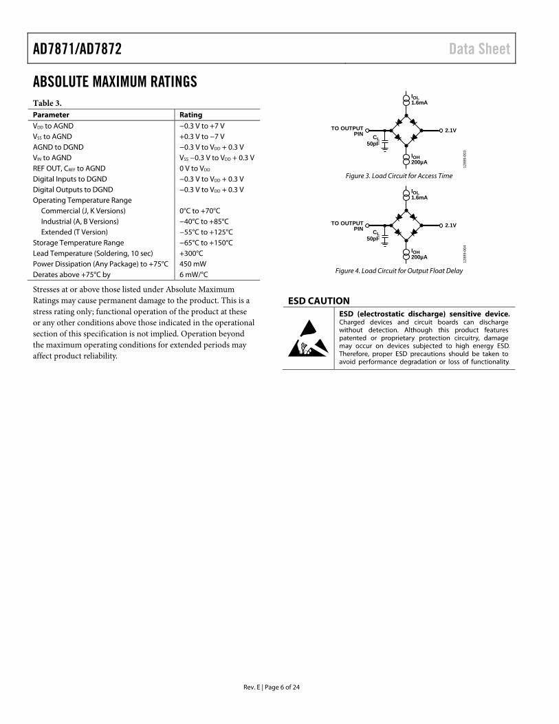
Figure 3. Load Circuit for Access Time
Figure 4. Load Circuit for Output Float Delay
ESD CAUTION
IOL1.6mA
IOH200µA
2.1VTO OUTPUTPIN CL
50pF
1288
9-00
3
IOL1.6mA
IOH200µA
2.1VTO OUTPUTPIN CL
50pF
1288
9-00
4

Data Sheet AD7871/AD7872
PIN CONFIGURATION AND FUNCTION DESCRIPTIONS
Figure 5. AD7871 DIP
Figure 6. AD7871 PLCC
Table 4. AD7871 Pin Function Descriptions Pin No. Mnemonic Description 1 CONVST Convert Start. A low to high transition on this input puts the track/hold into the hold mode. This input is
asynchronous to the CLK. CS and RD must be held high for the duration of this pulse.
2 CS Chip Select. Active low logic input. The device is selected when this input is active. With CONVST tied low, a new conversion is initiated when CS goes low.
3 RD Read. Active low logic input. This input is used in conjunction with CS low to enable the data outputs.
4 BUSY/ INT Busy/Interrupt. Logic low output indicating converter status. See Figure 14, Figure 15, Figure 16, and Figure 17.
5 CLK Clock Input. An external TTL-compatible clock may be applied to this input. Alternatively, tying this pin to VSS enables the internal laser-trimmed oscillator.
6 DB13/HBEN Data Bit 13 (MSB)/High Byte Enable. The function of this pin is dependent on the state of the 14/8/CLK input (see Pin 28). When 14-bit data is selected, this pin provides the DB13 output. When either byte or serial data is selected, this pin becomes the HBEN logic input. HBEN is used for 8-bit bus interfacing. When HBEN is low, DB7 to DB0 is the lower byte of data. With HBEN high, DB7 to DB0 is the upper byte of data (see Table 5).
7 DB12/SSTRB Data Bit 12/Serial Strobe. When 14-bit data is selected, this pin provides the DB12 data output. Otherwise, it is an active low three-state output that provides a framing pulse for serial data.
8 DB11/SCLK Data Bit 11/Serial Clock. When 14-bit data is selected, this pin provides the DB11 data output. Otherwise, SCLK is the gated serial clock output that is derived from the internal or external ADC clock. If the 14/8/CLK input is held at −5 V, then the SCLK runs continuously. With 14/8/CLK at 0 V, it is gated off (three-state) after serial transmission is complete.
9 DB10/SDATA Data Bit 10/Serial Data. When 14-bit parallel data is selected, this pin provides the DB10 data output. Otherwise, it is the three-state serial data output used in conjunction with SCLK and SSTRB in serial data transmission. Serial data is valid on the falling edge of SCLK, when SSTRB is low.
10 to 13 DB9 to DB6 Three-State Data Outputs controlled by CS and RD. Their function depends on the state of the 14/8/CLK and the HBEN inputs. With 14/8/CLK high, they are always DB9 to DB6; with 14/8/CLK low, their function depends on HBEN (see Table 5).
14 DGND Digital Ground. Ground return for digital circuitry. 15 to 20 DB5/DB13
to DB0/DB8 Three-State Data Outputs controlled by CS and RD. Their function depends on the 14/8/CLK DB0/DB8 and HBEN inputs. With 14/8/CLK high, they are always DB5 to DB0; with 14/8/C LK low or −5 V, their function is controlled by HBEN (see Table 5).
21 VDD Positive Supply, +5 V ± 5%. 22 AGND Analog Ground. Ground reference for analog circuitry. 23 CREF Decoupling Point for On-Chip Reference. Connect a 10 nF capacitor between this pin and AGND. 24 NC No Connect. 25 REFOUT Voltage Reference Output. The internal 3 V reference is provided at this pin. The external load capability is 500 µA.
CONVST 1
CS 2
RD 3
BUSY/INT 4
14/8/CLK28
VSS27
VIN26
REFOUT25
CLK 5
DB13/HBEN 6
DB12/SSTRB 7
NC24
CREF23
AGND22
DB11/SCLK 8 VDD21
DB10/SDATA 9 DB0/DB820
DB9 10 DB1/DB919
DB8 11 DB2/DB1018
DB7 12 DB3/DB1117
DB6 13 DB4/DB1216
DGND 14 DB5/DB1315
AD7871TOP VIEW
(Not to Scale)
NOTES1. NC = NO CONNECT. 12
889-
005
AD7871TOP VIEW
(Not to Scale)
1 28 27 26234
5
6
7
8
9
10
11
25
24
23
22
21
20
19
CLK
DB13/HBEN
DB12/SSTRB
DB11/SCLK
DB10/SDATA
DB9
DB8
REFOUT
NC
CREF
AGND
VDD
DB0/DB8
DB1/DB9
BU
SY/IN
T
RD
CS
CO
NVS
T
14/8
/CLK
V SS
V IN
DB
7
DB
6
DG
ND
DB
5/D
B13
DB
4/D
B12
DB
3/D
B11
DB
2/D
B10
12 13 14 15 16 17 18
NOTES1. NC = NO CONNECT. 12
889-
006
Rev. E | Page 7 of 24

AD7871/AD7872 Data Sheet
Pin No. Mnemonic Description 26 VIN Analog Input. The input range is ±3 V. 27 VSS Negative Supply, –5 V ± 5%. 28 14/8/CLK Three-Function Input. Defines both the parallel and serial data formats. With this pin at +5 V, the output data is
14-bit parallel only. With this pin at 0 V, both byte and serial data are available, and the SCLK is noncontinuous. With this pin at –5 V, both byte and serial data are available and the SCLK is continuous.
Table 5. Byte Output Format HBEN DB7 DB6 DB5 DB4 DB3 DB2 DB1 DB0 HIGH LOW LOW DB13 DB12 DB11 DB10 DB9 DB8 LOW DB7 DB6 DB5 DB4 DB3 DB2 DB1 DB0
Figure 7. AD7872 DIP, SOIC
Table 6. AD7872 Pin Function Descriptions Pin No. Mnemonic Description 1 CONTROL Control Input. With this pin at 0 V, the SCLK is noncontinuous; with this pin at −5 V, the SCLK is continuous. 2 CONVST Convert Start. A low to high transition on this input puts the track/hold into the hold mode. This input is
asynchronous to the CLK. 3 CLK Clock Input. An external TTL-compatible clock may be applied to this input. Alternatively, tying this pin to VSS
enables the internal laser-trimmed oscillator. 4 SSTRB Serial Strobe. This is an active low three-state output that provides a framing pulse for serial data. An external
4.7 kΩ pull-up resistor is required on SSTRB.
5 SCLK Serial Clock. SCLK is the gated serial clock output derived from the internal or external ADC clock. If the 14/8/ CLK input is at −5 V, then the SCLK runs continuously. With CONTROL at 0 V, it is gated off (three-state) after the serial transmission is complete. SCLK is an open-drain output and requires an external 2 kΩ pull-up resistor.
6 SDATA Serial Data. This is the three-state serial data output used in conjunction with SCLK and SSTRB in a serial data transmission. Serial data is valid on the falling edge of SCLK, when SSTRB is low. An external 4.7 kΩ pull-up resistor is required on SDATA.
7 NC No Connect. 8 DGND Digital Ground. Ground return for digital circuitry. 9 VDD Positive Supply for Analog Circuitry, +5 V ± 5%. 10 NC No Connect. 11 CREF Decoupling Point for On-Chip Reference. Connect a 10 nF capacitor between this pin and AGND. 12 AGND Analog Ground. Ground reference for analog circuitry. 13 REFOUT Voltage Reference Output. The internal 3 V reference is provided at this pin. The external load capability is
500 µA. 14 VIN Analog Input. The input range is ±3 V. 15 VSS Negative Supply, −5 V ± 5%. 16 VDD Positive Supply for Analog Circuitry, +5 V ± 5%. Connect Pin 16 and Pin 9 together.
NOTES1. NC = NO CONNECT.
CONTROL 1
CONVST 2
CLK 3
SSTRB 4
VDD16
VSS15
VIN14
REFOUT13
SCLK 5
SDATA 6
NC 7
AGND12
CREF11
NC10
DGND 8 VDD9
AD7872TOP VIEW
(Not to Scale)
1288
9-00
7
Rev. E | Page 8 of 24
Data Sheet AD7871/AD7872
Rev. E | Page 9 of 24
THEORY OF OPERATION CONVERTER DETAILS The AD7871/AD7872 is a complete 14-bit ADC, requiring no external components apart from power supply decoupling capacitors. It is comprised of a 14-bit successive approximation ADC based on a fast settling voltage-output DAC, a high speed comparator and CMOS SAR, a track-and-hold amplifier, a 3 V buried Zener reference, a clock oscillator, and control logic.
INTERNAL REFERENCE The AD7871/AD7872 have an on-chip temperature compensated buried Zener reference that is factory trimmed to 3 V ± 0 mV. Internally it provides both the DAC reference and the dc bias required for bipolar operation. Reference noise is minimized by connecting a capacitor between CREF and AGND. For specified operation this capacitor should be 10 nF. The reference output is available (REF OUT) and capable of providing up to 500 μA to an external load.
The maximum recommended capacitance on REF OUT for normal operation is 50 pF. If the reference is required for use external to the AD7871/AD7872, decouple it with a 200 Ω resistor in series with a parallel combination of a 10 μF tantalum capacitor and a 0.1 μF ceramic capacitor. These decoupling components are required to remove voltage spikes caused by the internal operation of the AD7871/AD7872.
Figure 8. Reference Circuit
TRACK-AND-HOLD AMPLIFIER The track-and-hold amplifier on the analog input of the AD7871/AD7872 allows the ADC to accurately convert an input sine wave of 6 V peak-peak amplitude to 14-bit accuracy. The input bandwidth of the track-and-hold amplifier is much greater than the Nyquist rate of the ADC even when the ADC is operated at its maximum throughput rate. The 0.1 dB cutoff frequency occurs typically at 500 kHz. The track-and-hold amplifier acquires an input signal to 14-bit accuracy in less than 2 μs. The overall throughput rate is determined by the conversion time plus the track-and-hold amplifier acquisition time. For a 2 MHz input clock, the throughput time is 12 μs maximum.
The operation of the track-and-hold amplifier is essentially transparent to the user. The track-and-hold amplifier goes from its tracking mode to its hold mode at the start of conversion. If the CONVST input is used to start conversion, then the track to hold transition occurs on the rising edge of CONVST. If CS on the AD7871 starts conversion, this transition occurs on the falling edge of CS.
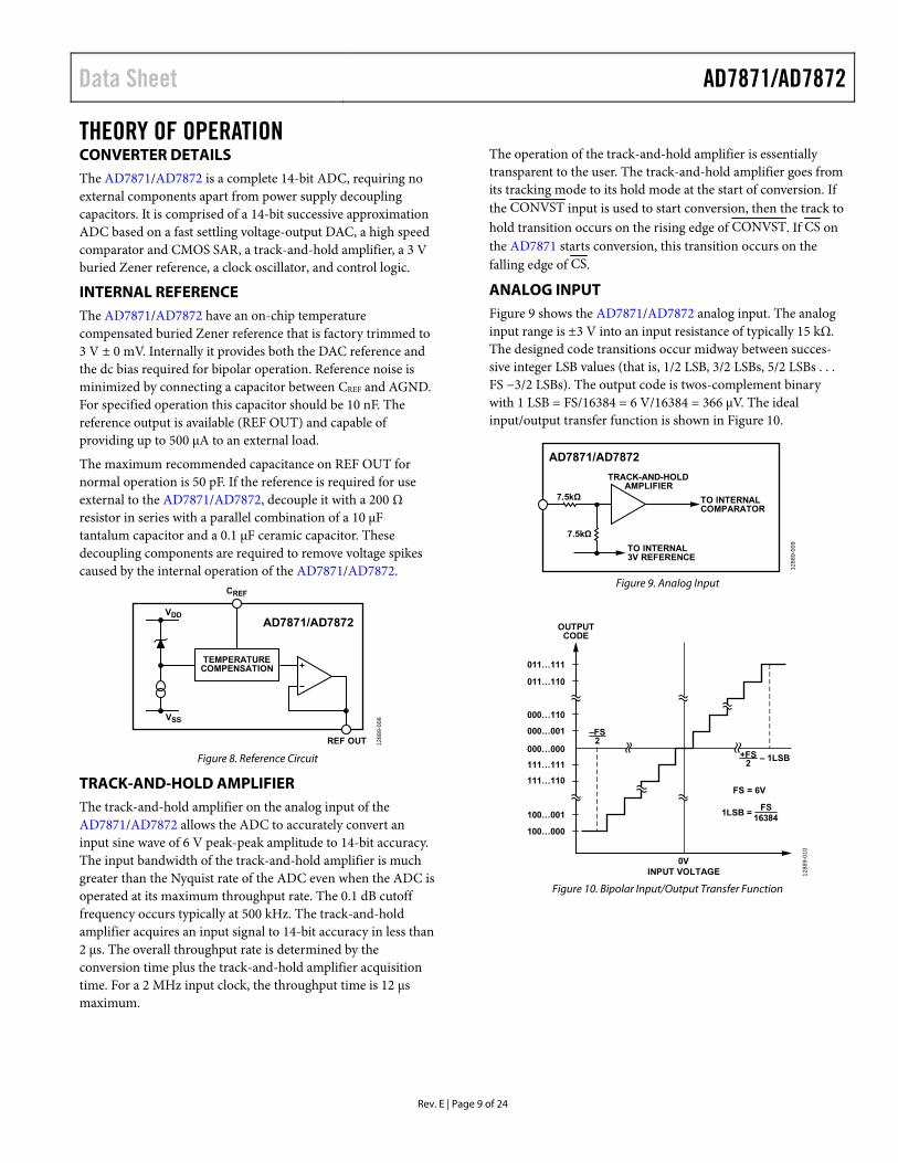
ANALOG INPUT Figure 9 shows the AD7871/AD7872 analog input. The analog input range is ±3 V into an input resistance of typically 15 kΩ. The designed code transitions occur midway between succes-sive integer LSB values (that is, 1/2 LSB, 3/2 LSBs, 5/2 LSBs . . . FS −3/2 LSBs). The output code is twos-complement binary with 1 LSB = FS/16384 = 6 V/16384 = 366 μV. The ideal input/output transfer function is shown in Figure 10.
Figure 9. Analog Input
Figure 10. Bipolar Input/Output Transfer Function
TEMPERATURECOMPENSATION
AD7871/AD7872
REF OUT
VSS
VDD
CREF
1288
9-00
8
AD7871/AD7872
TRACK-AND-HOLDAMPLIFIER
TO INTERNAL3V REFERENCE
7.5kΩ
7.5kΩ TO INTERNALCOMPARATOR
1288
9-00
9
011…111
OUTPUTCODE
011…110
100…001
100…000
0VINPUT VOLTAGE
000…110
000…001
000…000
111…111
111…110
–FS2
+FS – 1LSB2
FS1LSB =
FS = 6V
16384
1288
9-01
0
AD7871/AD7872 Data Sheet
BIPOLAR OFFSET SCALE ADJUSTMENT When the offset and full-scale errors of the AD7871/AD7872 need to be adjusted, offset error must be adjusted first. This is achieved by trimming the offset of the op amp driving the analog input of the AD7871/AD7872 while the input voltage is ½ LSB below AGND. The trim procedure is as follows: apply a voltage of −0.183 mV (−½ LSB) at V1 in Figure 11 and adjust the op amp offset voltage until the ADC output code flickers between 11 1111 1111 1111 and 00 0000 0000 0000.
Figure 11. Bipolar Adjust Circuit
Gain error can be adjusted at either the first code transition (ADC negative full scale) or the last code transition (ADC positive full scale). The trim procedures for both cases are in the following sections (see Figure 11).
Positive Full-Scale Adjust
Apply a voltage of 2.9995 V (FS/2 −3/2 LSBs) at V1 and adjust R2 until the ADC output code flickers between 01 1111 1111 1110 and 01 1111 1111 1111.
Negative Full-Scale Adjust
Apply a voltage of −2.9998 V (−FS/2 + 1/2 LSB) at V1 and adjust R2 until the ADC output code flickers between 10 0000 0000 0000 and 10 0000 0000 0001.
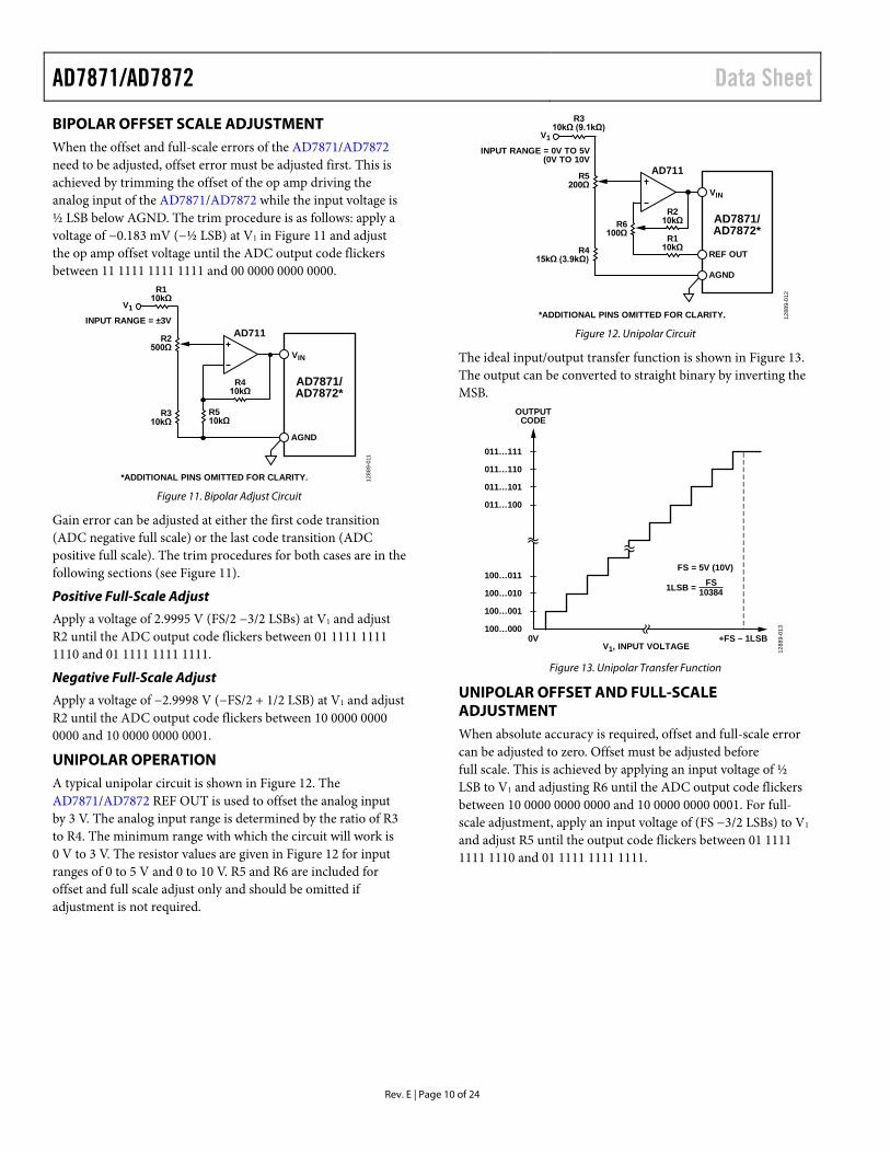
UNIPOLAR OPERATION A typical unipolar circuit is shown in Figure 12. The AD7871/AD7872 REF OUT is used to offset the analog input by 3 V. The analog input range is determined by the ratio of R3 to R4. The minimum range with which the circuit will work is 0 V to 3 V. The resistor values are given in Figure 12 for input ranges of 0 to 5 V and 0 to 10 V. R5 and R6 are included for offset and full scale adjust only and should be omitted if adjustment is not required.
Figure 12. Unipolar Circuit
The ideal input/output transfer function is shown in Figure 13. The output can be converted to straight binary by inverting the MSB.
Figure 13. Unipolar Transfer Function
UNIPOLAR OFFSET AND FULL-SCALE ADJUSTMENT When absolute accuracy is required, offset and full-scale error can be adjusted to zero. Offset must be adjusted before full scale. This is achieved by applying an input voltage of ½ LSB to V1 and adjusting R6 until the ADC output code flickers between 10 0000 0000 0000 and 10 0000 0000 0001. For full-scale adjustment, apply an input voltage of (FS −3/2 LSBs) to V1 and adjust R5 until the output code flickers between 01 1111 1111 1110 and 01 1111 1111 1111.
R110kΩ
R2500Ω
R310kΩ
AGND
VIN
R510kΩ
R410kΩ
AD7871/AD7872*
*ADDITIONAL PINS OMITTED FOR CLARITY.
V1
AD711INPUT RANGE = ±3V
1288
9-01
1
R310kΩ (9.1kΩ)
R5200Ω
R415kΩ (3.9kΩ)
AGND
REF OUT
VIN
R6100Ω
AD7871/AD7872*
*ADDITIONAL PINS OMITTED FOR CLARITY.
V1
AD711
INPUT RANGE = 0V TO 5V(0V TO 10V
R110kΩ
R210kΩ
1288
9-01
2
OUTPUTCODE
100…011
100…010
100…001
100…000
V1, INPUT VOLTAGE
011…101
011…100
011…111
011…110
FS1LSB =
FS = 5V (10V)
+FS – 1LSB0V
10384
1288
9-01
3
Rev. E | Page 10 of 24
Data Sheet AD7871/AD7872
TIMING AND CONTROL The conversion time for both external and internal clocks can vary from 19 to 20 rising clock edges depending on the conversion start to ADC clock synchronization. If a conversion is initiated within 30 ns prior to a rising edge of the ADC clock, the conversion time will consist of 20 rising clock edges.
There are two basic operating modes for the AD7871. In the first mode (Mode 1), the CONVST line is used to start a conversion and drive the track/hold into its hold mode. At the end of the conversion, the track/hold returns to its tracking mode. It is principally intended for digital signal processing and other applications where precise sampling in time is required. In these applications, it is important that the signal sampling occurs at exactly equal intervals to minimize errors due to sampling uncertainty or jitter. For these cases, the CONVST line is driven by a timer or some precise clock source.
The second mode is achieved by hard-wiring the CONVST line low. This mode (Mode 2) is intended for use in systems where the microprocessor has total control of the ADC, both initiating the conversion and reading the data. CS and RD start a conversion, and the microprocessor will normally be driven into a wait state for the duration of conversion by BUSY/INT. The AD7872 has one operating mode only: Mode 1, which uses CONVST to start conversion.
DATA OUTPUT FORMATS The AD7871 offers a choice of three data output formats: one serial and two parallel. The parallel data formats include a single 14-bit parallel word for 16-bit data buses and a two-byte format for 8-bit data buses. The data format is controlled by the 14/8/CLK input. A logic high on this pin selects the 14-bit parallel output format only. A logic low or −5 V applied to this pin allows the user access to either serial or byte formatted data. Three of the pins previously assigned to the four MSBs in parallel form are now used for serial communications while the fourth pin becomes a control input for the byte-formatted data. The three possible data output formats can be selected in either of the modes of operation.
The AD7872 is a serial output device only. The serial data format is exactly the same as the AD7871.
Parallel Output Format
The two parallel formats available on the AD7871 are a 14-bit wide data word and a 2-byte data word. In the first, all 14 bits of data are available at the same time on DB13 (MSB) through DB0 (LSB). In the second, two reads are required to access the data. When this data format is selected, the DB13/HBEN pin assumes the HBEN function. HBEN selects which byte of data is to be read from the AD7871. When HBEN is low, the lower eight bits of data are placed on the data bus during a read operation; with HBEN high, the upper six bits of the 14-bit word are placed on the data bus. These six bits are right justified and thereby occupy the lower six bits of the byte while the upper two bits are zeros.
Serial Output Format
Serial data is available on the AD7871 when the 14/8/CLK input is at 0 V or −5 V and in this case the DB12/SSTRB, DB11/SCLK and DB10/SDATA pins assume their serial functions. The AD7872 is a serial output device only. The serial function on both devices is identical. Serial data is available during conversion with a word length of 16 bits; two leading zeros, followed by the 14-bit conversion result starting with the MSB. The data is synchronized to the serial clock output (SCLK) and is framed by the serial strobe (SSTRB). Data is clocked out on a low to high transition of the serial clock and is valid on the falling edge of this clock while the SSTRB output is low. SSTRB goes low at the start of conversion and the first serial data bit (which is the first leading zero) is valid on the first falling edge of SCLK. All the serial lines are open-drain outputs and require external pull-up resistors.
The serial clock out is derived from the ADC master clock source which may be internal or external. Normally, SCLK is required during the serial transmission only. In these cases it can be shut down (that is, placed into three-state) at the end of the conversion to allow multiple ADCs to share a common serial bus. However, some serial systems require a serial clock that runs continuously. Both options are available on the AD7871 and AD7872. With the 14/8/CLK input on the AD7871 at −5 V, the serial clock (SCLK) runs continuously; when 14/8/CLK is at 0 V, SCLK goes into three-state at the end of transmission. The CONTROL pin on the AD7872 performs the same function. When this is at 0 V, SCLK is noncontinuous and when it is at −5 V, SCLK is continuous.
The SCLK, SDATA, and SSTRB lines are open-drain outputs. If these are required to drive capacitive loads in excess of 35 pF, buffering is recommended.
Rev. E | Page 11 of 24
AD7871/AD7872 Data Sheet
Rev. E | Page 12 of 24
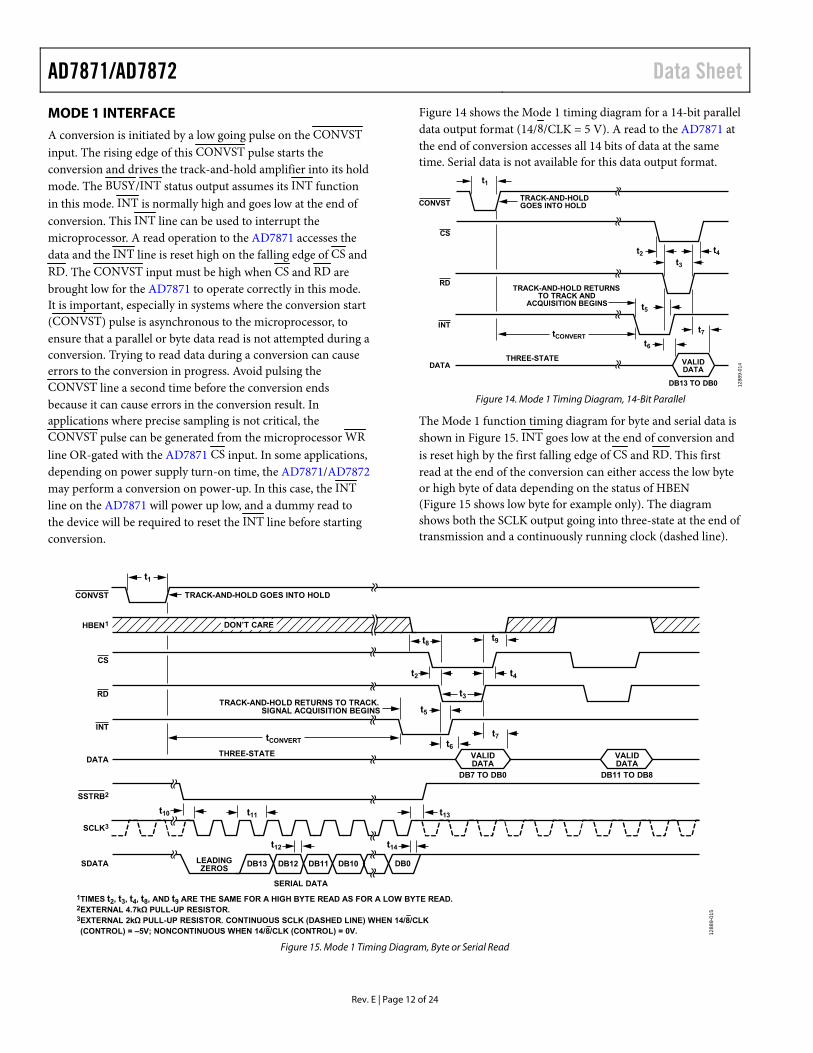
MODE 1 INTERFACE
A conversion is initiated by a low going pulse on the CONVST input. The rising edge of this CONVST pulse starts the conversion and drives the track-and-hold amplifier into its hold mode. The BUSY/INT status output assumes its INT function in this mode. INT is normally high and goes low at the end of conversion. This INT line can be used to interrupt the microprocessor. A read operation to the AD7871 accesses the data and the INT line is reset high on the falling edge of CS and RD. The CONVST input must be high when CS and RD are brought low for the AD7871 to operate correctly in this mode. It is important, especially in systems where the conversion start (CONVST) pulse is asynchronous to the microprocessor, to ensure that a parallel or byte data read is not attempted during a conversion. Trying to read data during a conversion can cause errors to the conversion in progress. Avoid pulsing the CONVST line a second time before the conversion ends because it can cause errors in the conversion result. In applications where precise sampling is not critical, the CONVST pulse can be generated from the microprocessor WR line OR-gated with the AD7871 CS input. In some applications, depending on power supply turn-on time, the AD7871/AD7872 may perform a conversion on power-up. In this case, the INT line on the AD7871 will power up low, and a dummy read to the device will be required to reset the INT line before starting conversion.
Figure 14 shows the Mode 1 timing diagram for a 14-bit parallel data output format (14/8/CLK = 5 V). A read to the AD7871 at the end of conversion accesses all 14 bits of data at the same time. Serial data is not available for this data output format.
Figure 14. Mode 1 Timing Diagram, 14-Bit Parallel
The Mode 1 function timing diagram for byte and serial data is shown in Figure 15. INT goes low at the end of conversion and is reset high by the first falling edge of CS and RD. This first read at the end of the conversion can either access the low byte or high byte of data depending on the status of HBEN (Figure 15 shows low byte for example only). The diagram shows both the SCLK output going into three-state at the end of transmission and a continuously running clock (dashed line).
Figure 15. Mode 1 Timing Diagram, Byte or Serial Read
CONVSTTRACK-AND-HOLDGOES INTO HOLD
TRACK-AND-HOLD RETURNSTO TRACK AND
ACQUISITION BEGINS
THREE-STATE VALIDDATA
DB13 TO DB0
CS
RD
INT
DATA
t2
t1
tCONVERT
t5
t6
t7
t4
t3
1288
9-01
4
SSTRB2
DATA
TRACK-AND-HOLD RETURNS TO TRACK.SIGNAL ACQUISITION BEGINS
TRACK-AND-HOLD GOES INTO HOLD
THREE-STATE VALIDDATA
DB7 TO DB0
VALIDDATA
DB11 TO DB8
HBEN1
t1
1TIMES t2, t3, t4, t8, AND t9 ARE THE SAME FOR A HIGH BYTE READ AS FOR A LOW BYTE READ.2EXTERNAL 4.7kΩ PULL-UP RESISTOR.3EXTERNAL 2kΩ PULL-UP RESISTOR. CONTINUOUS SCLK (DASHED LINE) WHEN 14/8/CLK(CONTROL) = –5V; NONCONTINUOUS WHEN 14/8/CLK (CONTROL) = 0V.
INT
RD
t8
t2 t4
t3
t9
t7
t5
tCONVERT t6
CONVST
CS
DB13 DB12 DB11 DB10
SCLK3
LEADINGZEROS
SDATA
SERIAL DATA
DB0
t11t10
t12
t13
t14
DON’T CARE
1288
9-01
5
Data Sheet AD7871/AD7872
Rev. E | Page 13 of 24
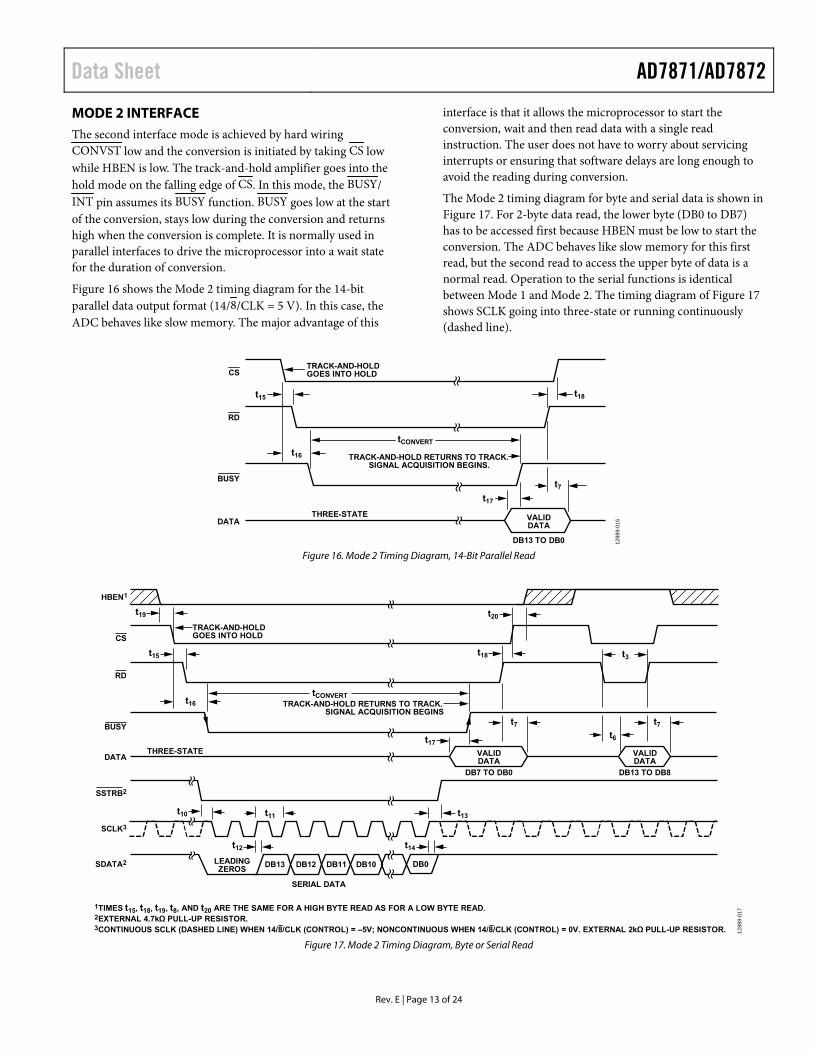
MODE 2 INTERFACE The second interface mode is achieved by hard wiring CONVST low and the conversion is initiated by taking CS low while HBEN is low. The track-and-hold amplifier goes into the hold mode on the falling edge of CS. In this mode, the BUSY/ INT pin assumes its BUSY function. BUSY goes low at the start of the conversion, stays low during the conversion and returns high when the conversion is complete. It is normally used in parallel interfaces to drive the microprocessor into a wait state for the duration of conversion.
Figure 16 shows the Mode 2 timing diagram for the 14-bit parallel data output format (14/8/CLK = 5 V). In this case, the ADC behaves like slow memory. The major advantage of this
interface is that it allows the microprocessor to start the conversion, wait and then read data with a single read instruction. The user does not have to worry about servicing interrupts or ensuring that software delays are long enough to avoid the reading during conversion.
The Mode 2 timing diagram for byte and serial data is shown in Figure 17. For 2-byte data read, the lower byte (DB0 to DB7) has to be accessed first because HBEN must be low to start the conversion. The ADC behaves like slow memory for this first read, but the second read to access the upper byte of data is a normal read. Operation to the serial functions is identical between Mode 1 and Mode 2. The timing diagram of Figure 17 shows SCLK going into three-state or running continuously (dashed line).
Figure 16. Mode 2 Timing Diagram, 14-Bit Parallel Read
Figure 17. Mode 2 Timing Diagram, Byte or Serial Read
CSTRACK-AND-HOLDGOES INTO HOLD
TRACK-AND-HOLD RETURNS TO TRACK.SIGNAL ACQUISITION BEGINS.
THREE-STATE VALIDDATA
DB13 TO DB0
RD
BUSY
DATA
t15
t17
t7
t16
tCONVERT
t18
1288
9-01
6
DATA
TRACK-AND-HOLD RETURNS TO TRACK.SIGNAL ACQUISITION BEGINS
THREE-STATE VALIDDATA
DB7 TO DB0
VALIDDATA
DB13 TO DB8
SSTRB2
BUSY
RD
tCONVERT
1TIMES t15, t18, t19, t8, AND t20 ARE THE SAME FOR A HIGH BYTE READ AS FOR A LOW BYTE READ.2EXTERNAL 4.7kΩ PULL-UP RESISTOR.3CONTINUOUS SCLK (DASHED LINE) WHEN 14/8/CLK (CONTROL) = –5V; NONCONTINUOUS WHEN 14/8/CLK (CONTROL) = 0V. EXTERNAL 2kΩ PULL-UP RESISTOR.
CS
DB13 DB12 DB11 DB10
SCLK3
LEADINGZEROS
SDATA2
SERIAL DATA
DB0
t11t10
t12
t13
t14
HBEN1
t19
t15
t16
TRACK-AND-HOLDGOES INTO HOLD
t20
t18 t3
t17
t7
t6
t7
1288
9-01
7

AD7871/AD7872 Data Sheet
DYNAMIC SPECIFICATIONS The AD7871/AD7872 are specified and tested for dynamic performance specifications as well as traditional dc specifications such as INL and DNL. These ac specifications are required for signal processing applications such as speech recognition, spectrum analysis and high speed modems. These applications require information on the effects on the spectral content of the input signal. Therefore, the parameters for which the AD7871/AD7872 is specified include SNR, harmonic distortion, intermodulation distortion, and peak harmonics. These terms are discussed in more detail in the following sections.
Signal-to-Noise Ratio (SNR)
SNR is the measured signal-to-noise ratio at the output of the ADC. The signal is the rms magnitude of the fundamental. Noise is the rms sum of all the nonfundamental signals up to half the sampling frequency (fS/2) excluding dc. SNR is dependent upon the number of quantization levels used in the digitization process; the more levels, the smaller the quantization noise. The theoretical signal to noise ratio for a sine wave input is given by:
SNR(dB) = (6.02N + 1.76) (1)
where N is the number of bits in the ADC. Thus, for an ideal 14-bit converter, SNR = 86 dB.
The output spectrum from the ADC is evaluated by applying a sine wave signal of very low distortion to the VIN input, which is sampled at an 83 kHz sampling rate. A Fast Fourier Transform (FFT) plot is generated from which the SNR data can be obtained. Figure 18 shows a typical 2048 point FFT plot of the AD7871/AD7872, with an input signal of 10 kHz and a sampling frequency of 83 kHz. The SNR obtained from this graph is 80 dB. Note that the harmonics are included when calculating the SNR.
Figure 18. Fast Fourier Transform Plot
Effective Number of Bits
The formula given in Equation 1 relates the SNR to the number of bits. Rewriting the formula, as in Equation 2, it is possible to
get a measure of performance expressed in an effective number of bits (N).
02.676.1−
=SNRN (2)
The effective number of bits for a device can be calculated directly from its measured SNR. Figure 19 shows a typical plot of effective number of bits vs. frequency for the AD7871/AD7872 with a sampling frequency of 60 kHz.
Figure 19. Effective Number of Bits vs. Frequency
Harmonic Distortion
Harmonic distortion is the ratio of the rms sum of harmonics to the fundamental. For the AD7871/AD7872, total harmonic distortion (THD) is defined as
1
26
25
24
23
22
VVVVVV
logdBTHD++++
= 20)(
where: V1 is the rms amplitude of the fundamental. V2, V3, V4, V5 and V6 are the rms amplitudes of the second through the sixth harmonic.
The THD is also derived from the FFT plot of the ADC output spectrum. Figure 20 shows how the THD varies with input frequency.
Figure 20. Total Harmonic Distortion vs. Frequency
0
–150
–120
–90
–60
–30
0 10 20 30
SIG
NA
L A
MPL
ITU
DE
(dB
)
FREQUENCY (kHz)
INPUT FREQUENCY = 10kHzSAMPLE FREQUENCY = 60kHzSNR = 80dBTA = 25°C
1288
9-01
8
14.0
12.0
12.5
13.0
13.5
0 10 20 30
NU
MB
ER (B
its)
FREQUENCY (kHz)
SAMPLE FREQUENCY = 60kHzTA = 25°C
1288
9-01
9
110
80
90
100
0 10 20 30
THD
(dB
)
INPUT FREQUENCY (kHz)
SAMPLE FREQUENCY = 60kHzTA = 25°C
1288
9-02
0
Rev. E | Page 14 of 24
Data Sheet AD7871/AD7872
Rev. E | Page 15 of 24
Intermodulation Distortion
With inputs consisting of sine waves at two frequencies, fa and fb, any active device with nonlinearities will create distortion products at sum and difference frequencies of mfa ± nfb where m, n = 0, 1, 2, 3, etc. Intermodulation terms are those for which neither m nor n are equal to zero. For example, the second order terms include (fa + fb) and (fa – fb), while the third order terms include (2fa + fb), (2fa – fb), (fa + 2fb) and (fa – 2fb).
Using the CCIF standard where two input frequencies near the top end of the input bandwidth are used, the second- and third-order terms are of different significance. The second-order terms are usually distanced in frequency from the original sine waves while the third-order terms are usually at a frequency close to the input frequencies. As a result, the second- and third-order terms are specified separately. The calculation of the intermodulation distortion is as per the THD specification, where it is the ratio of the rms sum of the individual distortion products to the rms amplitude of the fundamental expressed in decibels. In this case, the input consists of two, equal amplitude, low distortion sine waves. Figure 21 shows a typical IMD plot for the AD7871/AD7872.
Figure 21. IMD Plot
Peak Harmonic or Spurious Noise
Peak harmonic or spurious noise is defined as the ratio of the rms value of the next largest component in the ADC output spectrum (up to fS/2 and excluding dc) to the rms value of the fundamental. Normally, the value of this specification will be determined by the largest harmonic in the spectrum, but for parts where the harmonics are buried in the noise floor, peak will be a noise peak.
MICROPROCESSOR INTERFACE The AD7871/AD7872 have a wide variety of interfacing options. The AD7871 offers two operating modes and three data-output formats, while the AD7872 is a dedicated serial output device. The fast data access times on the parallel modes of the AD7871 allow interfacing to the very fast DSPs. The serial mode on both the AD7871 and AD7872 is compatible with the serial port structures on all the popular DSPs.
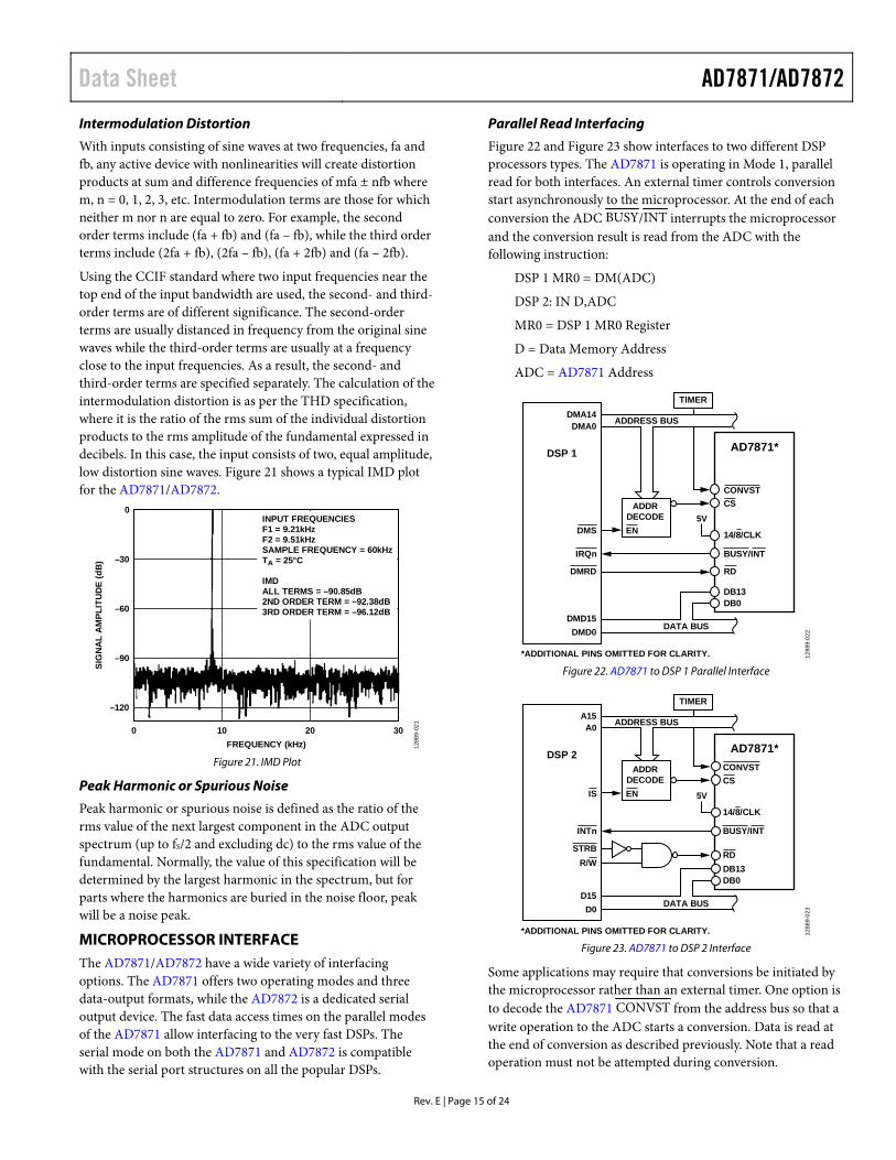
Parallel Read Interfacing
Figure 22 and Figure 23 show interfaces to two different DSP processors types. The AD7871 is operating in Mode 1, parallel read for both interfaces. An external timer controls conversion start asynchronously to the microprocessor. At the end of each conversion the ADC BUSY/INT interrupts the microprocessor and the conversion result is read from the ADC with the following instruction:
DSP 1 MR0 = DM(ADC)
DSP 2: IN D,ADC
MR0 = DSP 1 MR0 Register
D = Data Memory Address
ADC = AD7871 Address
Figure 22. AD7871 to DSP 1 Parallel Interface
Figure 23. AD7871 to DSP 2 Interface
Some applications may require that conversions be initiated by the microprocessor rather than an external timer. One option is to decode the AD7871 CONVST from the address bus so that a write operation to the ADC starts a conversion. Data is read at the end of conversion as described previously. Note that a read operation must not be attempted during conversion.
0
–120
–90
–60
–30
0 10 20 30
SIG
NA
L A
MPL
ITU
DE
(dB
)
FREQUENCY (kHz)
INPUT FREQUENCIESF1 = 9.21kHzF2 = 9.51kHzSAMPLE FREQUENCY = 60kHzTA = 25°C
IMDALL TERMS = –90.85dB2ND ORDER TERM = –92.38dB3RD ORDER TERM = –96.12dB
1288
9-02
1DMA14
DMA0
CONVST
TIMER
CS5V
14/8/CLK
BUSY/INT
RD
DB13DB0
*ADDITIONAL PINS OMITTED FOR CLARITY.
ADDRESS BUS
DATA BUS
ADDRDECODEENDMS
IRQn
DMRD
DMD15DMD0
AD7871*DSP 1
1288
9-02
2
A15A0
CONVST
TIMER
CS5V
14/8/CLK
BUSY/INT
RDDB13DB0
ADDRESS BUS
DATA BUS
ADDRDECODEENIS
INTn
STRB
D15D0
R/W
DSP 2
*ADDITIONAL PINS OMITTED FOR CLARITY.
AD7871*
1288
9-02
3

AD7871/AD7872 Data Sheet
Rev. E | Page 16 of 24
Serial Interfacing
Both the AD7871 and the AD7872 have an identical serial interface. The diagrams that follow show the AD7872 interfaces only, but the AD7871 could just as easily be used in these circuits. Figure 24, Figure 25, and Figure 26 show the AD7872 connected to three popular DSPs. In all three interfaces, CONVST is used to start the conversion because this does not activate the parallel bus. Thus, the microprocessor can continue to use its parallel bus regardless of the state of the AD7872. The interfaces show a timer driving the CONVST input but this could be generated from a decoded address if required.
AD7872 to DSP Type 1 Serial Interface
Figure 24 shows a serial interface between the AD7872 and DSP Type 1. The interface arrangement is two-wire with the AD7872 configured for noncontinuous clock operation CONTROL = 0 V). DSP Type 1 is configured for normal mode asynchronous operation with gated clock. It is set up for a 16-bit word with SCK as an input and the FSL control bit set to a 0. In this configuration, the DSP Type 1 assumes valid data on the first falling edge of SCK. Because the AD7872 provides valid data on this first edge, there is no need for a strobe or framing pulse for the data. SCLK and SDATA are three-stated when the AD7872 is not performing a conversion. During conversion, data is valid on the SDATA output of the AD7872 and is clocked into the Receive Data Shift Register of DSP Type 1. When this register has received 16 bits of data, it generates an internal interrupt on DSP Type 1 to read the data from the register.
Figure 24. AD7872 to DSP Type 1 Interface
DSP Type 1 and AD7872 can also be configured for continuous clock operation. In this case a strobe pulse is required by DSP Type 1 to indicate when data is valid. The SSTRB output of the AD7872 is inverted and applied to the SC1 input of DSP Type 1 to provide this strobe pulse. All other conditions and connections are the same as for the gated clock operation.
AD7872 to DSP Type 2 Serial Interface
Figure 25 shows a serial interface between the AD7872 and DSP Type 2. The AD7872 is configured for continuous clock operation. Note that the ADC will not interface correctly to a DSP if it is configured for a noncontinuous clock. Data is clocked into the data receive register (DRR) of a DSP during conversion. As with the previous interfaces, when a 16-bit word is received by the DSP it generates an internal interrupt to read the data from the DRR.
Figure 25. AD7872 to DSP Type 2 Interface
AD7872 to a DSP Microcomputer Serial Interface
Figure 26 shows a serial interface between the AD7872 and a DSP microcomputer. The AD7872 is configured for continuous clock operation. Data is clocked into the serial port register of the microcomputer during conversion. As with the previous interfaces, when a 16-bit data word is received by a DSP microcomputer an internal microprocessor interrupt is generated and the data is read from the serial port register.
Figure 26. AD7872 to a DSP Microcomputer Serial Interface
STANDALONE OPERATION The AD7871 can be used in its Mode 2, parallel mode for standalone operation. In this case, conversion is initiated with a pulse to the CS input. This pulse must be longer than the conversion time of the ADC. The BUSY output is used to drive the RD input. Data is latched from the AD7871 DB0 to DB11 outputs to an external latch on the rising edge of BUSY.
CONVST
CONTROL
SCLK
2kΩ
5V
4.7kΩ
SDATA
SCK
SRD
DSPTYPE 1
TIMER
*ADDITIONAL PINS OMITTED FOR CLARITY.
AD7872*
1288
9-02
4
CONVST
CONTROL
2kΩ
+5V
–5V
4.7kΩ 4.7kΩ
CLKR
FSR
DR
SCLK
SSTRB
SDATA
DSPTYPE 2
TIMER
1ADDITIONAL PINS OMITTED FOR CLARITY.
AD7872*
1288
9-02
5
CONVST
CONTROL
2kΩ
+5V
–5V
4.7kΩ 4.7kΩ
SCLK
FSR
DR
SCLK
SSTRB
SDATA
DSPMICROCOMPUTER
TIMER
*ADDITIONAL PINS OMITTED FOR CLARITY.
AD7872*
1288
9-02
6
Data Sheet AD7871/AD7872
APPLICATION INFORMATION Good printed circuit board (PCB) layout is as important as the circuit design itself in achieving high speed ADC performance. The AD7871/AD7872 is required to make bit decisions on an LSB size of 366 µV. Thus, the designer has to be conscious of noise both in the ADC itself and in the preceding analog circuitry. Switching mode power supplies are not recommended as the switching spikes will feed through to the comparator causing noisy code transitions. Other causes of concern are ground loops and digital feedthrough from microprocessors. These are factors that influence any ADC; a proper PCB layout that minimizes these effects is essential for best performance.
LAYOUT HINTS Ensure that the layout for the PCB has the digital and analog signal lines separated as much as possible. Take care not to run a digital track alongside an analog signal track. Guard (screen) the analog input with AGND.
Establish a single point analog ground (star ground) separate from the logic system ground at the AD7871/AD7872 AGND pin or as close as possible to the AD7871/AD7872. Connect all other grounds and the AD7871/AD7872 DGND to this single analog ground point. Do not connect any other digital grounds to this analog ground point.
Low impedance analog and digital power supply common returns are essential to low noise operation of the ADC, so make the foil width for these tracks as wide as possible. The use of ground planes minimizes impedance paths and also guards the analog circuitry from digital noise. The circuit layout of Figure 31 and Figure 32 have both analog and digital ground planes that are kept separated and joined together only at the AD7871/AD7872 AGND pin.
NOISE Keep the input signal leads to VIN and signal return leads from AGND as short as possible to minimize input noise coupling. In applications where this is not possible, use a shielded cable between the source and the ADC. Reduce the ground circuit impedance as much as possible because any potential difference in grounds between the signal source and the ADC appears as an error voltage in series with the input signal.
DATA ACQUISITION BOARD Figure 29 shows the AD7871/AD7872 in a data acquisition circuit. The corresponding PCB layout has three interface ports: one serial and two parallel. Note that the AD7871/AD7872 serial lines are buffered by a 74HC244. This allows long lines with large capacitive loads to be driven. One of the parallel ports is directly compatible with the DSP processor evaluation board expansion connector.
The only additional component required for a full data acquisition system is an antialiasing filter. There is a component grid provided near the analog input on the PCB, which may be used for such a filter or any other input conditioning circuitry. To facilitate this option, there is a shorting plug (labelled LK1 on the PCB) on the analog input track. If this shorting plug is used, the analog input connects to the buffer amplifier driving the AD7871/AD7872; if this shorting plug is omitted, a wire link can be used to connect the analog input to the PCB component grid.
Rev. E | Page 17 of 24

AD7871/AD7872 Data Sheet
Rev. E | Page 18 of 24
INTERFACE CONNECTIONS There are two parallel connectors labeled SKT4 and SKT6, and one serial connector labeled SKT5. A shorting plug option (LK3 in Figure 29) configures the ADC for the appropriate interface.
SKT6 is a 96-contact (3-row) Eurocard connector that is directly compatible with the DSP processor evaluation board prototype expansion connector. The expansion connector on the DSP processor has eight decoded chip enable outputs labeled ECE1 to ECE8. ECE6 is used to drive the AD7871 CS input on the board. To avoid selecting the on-board RAM sockets at the same time, remove LK6 on the DSP processor board. In addition, the DSP processor expansion connector has four interrupts labelled EIRQ0 to EIRQ3. The AD7871 BUSY/ INT output connects to EIRQ0. There is a single wait state generator connected to EDMACK to allow the AD7871 to interface to the faster versions of the DSP processor.
SKT4 is a 26-way (2-row) IDC connector. This contains the same signal contacts as SKT6 except for EDMACK, which is connected to SKT6 only. It also contains decoded R/W and STRB inputs necessary for DSP processor interfacing.
SKT5 is a 5-way D-type connector meant for serial interfacing only. An inverted DB11/SCLK output is also provided on this connector for systems that accept data on a rising clock edge.
SKT1, SKT2, and SKT3 are three BNC connectors providing connections for the analog input, the CONVST input and an external clock.
Figure 27. SKT4 Pinout
Figure 28. SKT5 Pinout
POWER SUPPLY CONNECTIONS The PCB requires two analog power supplies and one 5 V logic supply. The analog supplies are labelled V+ and V−, and the range for both supplies is 12 V to 15 V. Connection to the 5 V digital supply is made through any of the SKT4 to SKT6 connectors. The ±5 V supply required by the AD7871/AD7872 is generated from voltage regulators on the V+ and V− power supplies input (IC6 and IC7 in Figure 29).
SHORTING PLUG OPTIONS There are seven shorting plug options which must be set before using the board. These are outlined in Table 7.
Table 7. Plug Description LK1 Connects the analog input to a buffer amplifier. The
analog input may also be connected to a component grid for signal conditioning.
LK2 Selects either the AD7871/AD7872 internal clock or an external clock source.
LK3 Configures the AD7871 14/8/CLK input for the appropriate serial or parallel interface.
LK4 Connects the AD7871 RD input directly to the two parallel connectors or to a decoded STRB and R/W input.
LK5 Connects the R3 pull-up resistor to SSTRB. LK6 Connects the R4 pull-up resistor to SCLK. LK7 Connects the R5 pull-up resistor to SDATA.
Remove LK5 to LK7 for parallel interfacing.
1R/W3RD5CS7NC9DB12/SSTRB
NC = NO CONNECT
11DB10/SDATA13DB8/LOW15DB6/LOW17DB4/DB1219DB2/DB1021DB0/DB8235V25GND
2
4
6
8
10
12
14
16
18
20
22
24
26
STRBNCNCBUSY/INTDB13/HBENDB11/SCLKHB9/LOWDB7/LOWDB5/DB13DB3/DB11DB1/DB95VGND
1288
9-02
7
1
DB
12/S
STR
BN
C
NC = NO CONNECT
NC
NC
DG
ND
DB
11/S
CLK
DB
11/S
CLK
DB
10/S
DA
TA
5V
3 5
7 9
2 4
6 8
1288
9-02
8

Data Sheet AD7871/AD7872
Rev. E | Page 19 of 24
Figure 29. Data Acquisition Circuit Using the AD7871/AD7872
Figure 30. PCB Silkscreen for Figure 29
14/8/CLKCONTROL
ANALOGINPUT
±3V
SKT1
LK1
IC1AD711
C110µF
C20.1µF
C310µF
C40.1µF
C710µF
C80.1µF
SKT4 SKT5
PARALLEL COMMUNICATIONS PORT
25
SERIAL COMMUNICATIONS PORT
3 1 2 4 9 526 3 8 1 10 2 9 12 1113-23
RDDMRD
ECE6
VCCVCC
LK5 LK6 LK7
R3 R4 R5R1R2
CONVST
CLKSKT3
SKT2
VSS
LK2A
B
A
B
LK4
VCC
LK3ABC VSS
EIRQ0DMD15DMD14DMD13DMD12DMD11
DMD4
DGND A32
B7
C22
A31VCC
SKT6ADSP-2100
CONNECTOR+5V
A9B11B12B13B14B15B23
IC2/IC3
IC4IC4
IC4
BUSY/INTDB13/HBEN
DB12/SSTRBDB11/SCLK
DB10/SDATADB9/LOWDB0/DB8
CS
CLK
VDD
VSS
VIN
CREF
AGND
DGND DATA BUS
AD7871/AD7872
CONVST
V+VDDIN OUT
IC779L05GND
C510µF
C60.1µF
V–VSSIN OUT
IC679L05GND
V+
V–
C1910nF
CLK OUT
EDMACKVCC VCC
C6
B6
IC4
CLRDCLKIC5
74HC74
Q
5 23 24
VDD 2A3 2A1 2A22G IC8 VCC2Y3 2Y2 2Y1
HC244
VCC
1288
9-02
9
1288
9-03
0

AD7871/AD7872 Data Sheet
Figure 31. PCB Component Side Layout for Figure 29
Figure 32. PCB Solder Side Layout for Figure 29
1288
9-03
112
889-
032
Rev. E | Page 20 of 24

Data Sheet AD7871/AD7872
Rev. E | Page 21 of 24
OUTLINE DIMENSIONS
Figure 33. 16-Lead Plastic Dual In-Line Package [PDIP]
Narrow Body (N-16)
Dimensions shown in inches
Figure 34. 28-Lead Plastic Dual In-Line Package [PDIP]
Wide Body (N-28-3)
Dimensions shown in inches
COMPLIANT TO JEDEC STANDARDS MS-001-BB
0.0220.0180.015
0.1500.1300.115
0.0700.0600.055
0.0210.0160.0110.045
0.0390.030
0.1950.1300.115
16
18
9
0.100BSC
0.7750.7550.735
0.210MAX
0.015MIN
0.2800.2500.240
0.430MAX
0.0120.0100.008
0.3250.3100.300
0.015GAUGEPLANE
03-0
7-20
14-D
SEATINGPLANE
TOP VIEW
SIDE VIEW
END VIEW
PIN 1INDICATOR
COMPLIANT TO JEDEC STANDARDS MS-011
1.4501.440
0.5500.530
0.6060.594
15°8°
0.0600.020
0.0200.015
0.1050.095
0.1750.120
0.200MAX
0.005MIN
28
114
15
0.015GAUGEPLANE
01-1
3-20
15-A
SEATINGPLANE
TOP VIEW
SIDE VIEW
END VIEW
PIN 1INDICATOR
0.0700.0600.050
0.0120.0100.008
AD7871/AD7872 Data Sheet
Rev. E | Page 22 of 24
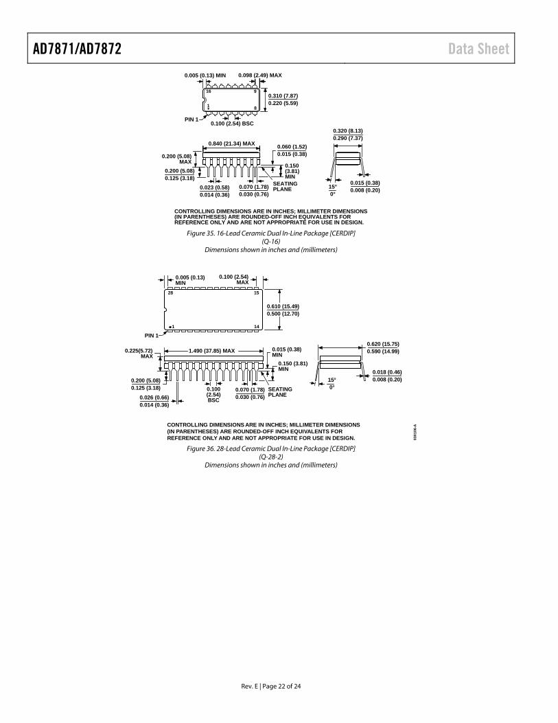
Figure 35. 16-Lead Ceramic Dual In-Line Package [CERDIP]
(Q-16) Dimensions shown in inches and (millimeters)
Figure 36. 28-Lead Ceramic Dual In-Line Package [CERDIP]
(Q-28-2) Dimensions shown in inches and (millimeters)
CONTROLLING DIMENSIONS ARE IN INCHES; MILLIMETER DIMENSIONS(IN PARENTHESES) ARE ROUNDED-OFF INCH EQUIVALENTS FORREFERENCE ONLY AND ARE NOT APPROPRIATE FOR USE IN DESIGN.
0.840 (21.34) MAX
15°0°
0.320 (8.13)0.290 (7.37)
0.015 (0.38)0.008 (0.20)
0.200 (5.08)MAX
0.200 (5.08)0.125 (3.18)
0.023 (0.58)0.014 (0.36)
0.310 (7.87)0.220 (5.59)
0.005 (0.13) MIN 0.098 (2.49) MAX
0.100 (2.54) BSCPIN 1
1 8
916
SEATINGPLANE
0.150(3.81)MIN
0.070 (1.78)0.030 (0.76)
0.060 (1.52)0.015 (0.38)
CONTROLLING DIMENSIONS ARE IN INCHES; MILLIMETER DIMENSIONS(IN PARENTHESES) ARE ROUNDED-OFF INCH EQUIVALENTS FORREFERENCE ONLY AND ARE NOT APPROPRIATE FOR USE IN DESIGN.
28
1 14
15
0.610 (15.49)0.500 (12.70)
0.005 (0.13)MIN
0.100 (2.54)MAX
0.620 (15.75)0.590 (14.99)
0.018 (0.46)0.008 (0.20)
SEATINGPLANE
0.225(5.72)MAX
1.490 (37.85) MAX
0.150 (3.81)MIN
0.200 (5.08)0.125 (3.18)
0.015 (0.38)MIN
0.026 (0.66)0.014 (0.36)
0.100(2.54)BSC
0.070 (1.78)0.030 (0.76)
15°0°
PIN 1
0301
06-A
Data Sheet AD7871/AD7872
Rev. E | Page 23 of 24
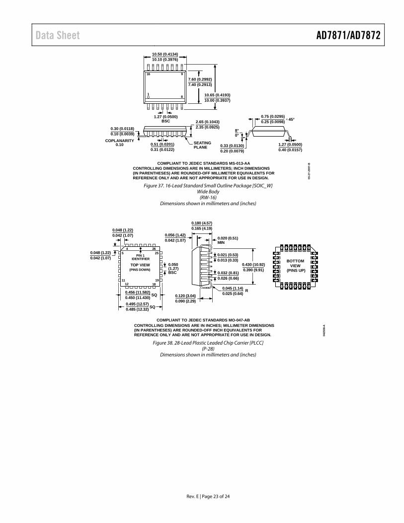
Figure 37. 16-Lead Standard Small Outline Package [SOIC_W]
Wide Body (RW-16)
Dimensions shown in millimeters and (inches)
Figure 38. 28-Lead Plastic Leaded Chip Carrier [PLCC]
(P-28) Dimensions shown in millimeters and (inches)
CONTROLLING DIMENSIONS ARE IN MILLIMETERS; INCH DIMENSIONS(IN PARENTHESES) ARE ROUNDED-OFF MILLIMETER EQUIVALENTS FORREFERENCE ONLY AND ARE NOT APPROPRIATE FOR USE IN DESIGN.
COMPLIANT TO JEDEC STANDARDS MS-013-AA
10.50 (0.4134)10.10 (0.3976)
0.30 (0.0118)0.10 (0.0039)
2.65 (0.1043)2.35 (0.0925)
10.65 (0.4193)10.00 (0.3937)
7.60 (0.2992)7.40 (0.2913)
0.75 (0.0295)0.25 (0.0098) 45°
1.27 (0.0500)0.40 (0.0157)
COPLANARITY0.10 0.33 (0.0130)
0.20 (0.0079)0.51 (0.0201)0.31 (0.0122)
SEATINGPLANE
8°0°
16 9
81
1.27 (0.0500)BSC
03-2
7-20
07-B
COMPLIANT TO JEDEC STANDARDS MO-047-ABCONTROLLING DIMENSIONS ARE IN INCHES; MILLIMETER DIMENSIONS(IN PARENTHESES) ARE ROUNDED-OFF INCH EQUIVALENTS FORREFERENCE ONLY AND ARE NOT APPROPRIATE FOR USE IN DESIGN.
45
2625
1112
1918
TOP VIEW(PINS DOWN)
SQ0.456 (11.582)0.450 (11.430)
0.050(1.27)BSC
0.048 (1.22)0.042 (1.07)
0.048 (1.22)0.042 (1.07)
0.495 (12.57)0.485 (12.32) SQ
0.021 (0.53)0.013 (0.33)
0.430 (10.92)0.390 (9.91)
0.032 (0.81)0.026 (0.66)
0.120 (3.04)0.090 (2.29)
0.056 (1.42)0.042 (1.07) 0.020 (0.51)
MIN
0.180 (4.57)0.165 (4.19)
BOTTOMVIEW
(PINS UP)
0.045 (1.14)0.025 (0.64)
R
PIN 1 IDENTIFIER
0425
08-A

AD7871/AD7872 Data Sheet
Rev. E | Page 24 of 24
ORDERING GUIDE Model1, 2, 3, 4 Temperature Range Package Description Package Option AD7871JN 0°C to +70°C 28-Lead PDIP N-28-3 AD7871JNZ 0°C to +70°C 28-Lead PDIP N-28-3 AD7871JP-REEL 0°C to +70°C 28-Lead PLCC P-28 AD7871JPZ 0°C to +70°C 28-Lead PLCC P-28 AD7871JPZ-REEL 0°C to +70°C 28-Lead PLCC P-28 AD7871KNZ 0°C to +70°C 28-Lead PDIP N-28-3 AD7871KPZ 0°C to +70°C 28-Lead PLCC P-28 AD7871TQ –55°C to +125°C 28-Lead CERDIP Q-28-2 AD7872AN –40°C to +85°C 16-Lead PDIP N-16 AD7872ANZ –40°C to +85°C 16-Lead PDIP N-16 AD7872BR –40°C to +85°C 16-Lead SOIC_W RW-16 AD7872BRZ –40°C to +85°C 16-Lead SOIC_W RW-16 AD7872BRZ-REEL –40°C to +85°C 16-Lead SOIC_W RW-16 AD7872JNZ 0°C to +70°C 16-Lead PDIP N-16 AD7872JRZ 0°C to +70°C 16-Lead SOIC_W RW-16 AD7872JRZ-REEL 0°C to +70°C 16-Lead SOIC_W RW-16 AD7872KNZ 0°C to +70°C 16-Lead PDIP N-16 AD7872KRZ 0°C to +70°C 16-Lead SOIC_W RW-16 AD7872KRZ-REEL 0°C to +70°C 16-Lead SOIC_W RW-16 AD7872TQ –55°C to +125°C 16-Lead CERDIP Q-16 1 Z = RoHS Compliant Part. 2 To order MIL-STD-883, Class B, processed parts, add /883B to part number. Contact local sales office for military data sheet. 3 Contact local sales office for LCCC availability. 4 The AD787xTQ models are available to /883B processing only.
©2015 Analog Devices, Inc. All rights reserved. Trademarks and registered trademarks are the property of their respective owners. D12889-0-1/15(E)