
Lab 2 - University of Manitoba
15
24.361 Lab. 2 10 ECE 3610 MICROPROCESSING SYSTEMS Laboratory 2 LAB 2: PROGRAMMING THE HCS12 P USING THE METROWERKS CODEWARRIOR DEVELOPMENT ENVIRONMENT 1 INTRODUCTION This lab will familiarize you with Freescale’s Microcontroller Unit, Student Learning Kit (MCUSLK) using the MC9S12C32 MCU application module. You will also gain familiarity with the Integrated Development Environment (IDE) and Metrowerks Code Warrior. You will learn (a) how to install and setup the software (actually, you will be just verifying it, because it is already installed on the host PC), (b) how to setup the hardware, by configuration of the MCU Project Board - 2 and the MC9S12C32, (c) how to start a new project using the CodeWarrior develop- ment environment, (d) how to modify memory locations and registers, (e) how to enter and run a simple assembly language program, and (f) how to use some of the debugging features. 1.1 OBJECTIVES This lab is intended as a tutorial, and so the objectives of this lab are to understand each of the topics covered. The Section 6 Experiment must be completed in the lab and submitted to the TA for marking. The Section 7 Points to Ponder must be answered in your log book and submitted to the TA for marking by the next day following the lab. Successful completion of the following labs depend on the knowledge and familiarity you are to gain in this lab. 1.2 APPARATUS Ensure you have the following components, which comprise the development worksta- tion: A host PC, MCU Project Board - 2, CSM-12C32 MCU application module, USB cable, and +- 15V Universal AC/DC adapter (see Fig. 9). 2 BACKGROUND: INTRODUCTION TO THE DEVELOPMENT WORKSTATION The development workstation consists of three main parts: a host computer (PC); a Uni- versal Serial Bus (USB) communications channel; the MCU Project Board - 2; and the CSM- 12C32 MCU application module. In this lab, we primarily use the PC to develop our software. The USB serves as a communications medium, allowing us to upload, run, and debug our pro- grams on the CSM-12C32 MCU. The MCU Project Board - 2 contains circuits and devices which are interfaced with the CSM-12C32 MCU. As well, there is a project board on which we can cre- ate, construct, and test prototype circuits and devices to interface with the CSM-12C32 MCU.
Transcript of Lab 2 - University of Manitoba

24.361 Lab. 2 10
ECE 3610 MICROPROCESSING SYSTEMS
Laboratory 2
LAB 2: PROGRAMMING THE HCS12 P USING THE METROWERKS CODEWARRIOR DEVELOPMENT ENVIRONMENT
1 INTRODUCTION
This lab will familiarize you with Freescale’s Microcontroller Unit, Student Learning Kit(MCUSLK) using the MC9S12C32 MCU application module. You will also gain familiarity withthe Integrated Development Environment (IDE) and Metrowerks Code Warrior. You will learn (a)how to install and setup the software (actually, you will be just verifying it, because it is alreadyinstalled on the host PC), (b) how to setup the hardware, by configuration of the MCU ProjectBoard - 2 and the MC9S12C32, (c) how to start a new project using the CodeWarrior develop-ment environment, (d) how to modify memory locations and registers, (e) how to enter and run asimple assembly language program, and (f) how to use some of the debugging features.
1.1 OBJECTIVES
This lab is intended as a tutorial, and so the objectives of this lab are to understand each ofthe topics covered. The Section 6 Experiment must be completed in the lab and submitted to theTA for marking. The Section 7 Points to Ponder must be answered in your log book and submittedto the TA for marking by the next day following the lab. Successful completion of the followinglabs depend on the knowledge and familiarity you are to gain in this lab.
1.2 APPARATUS
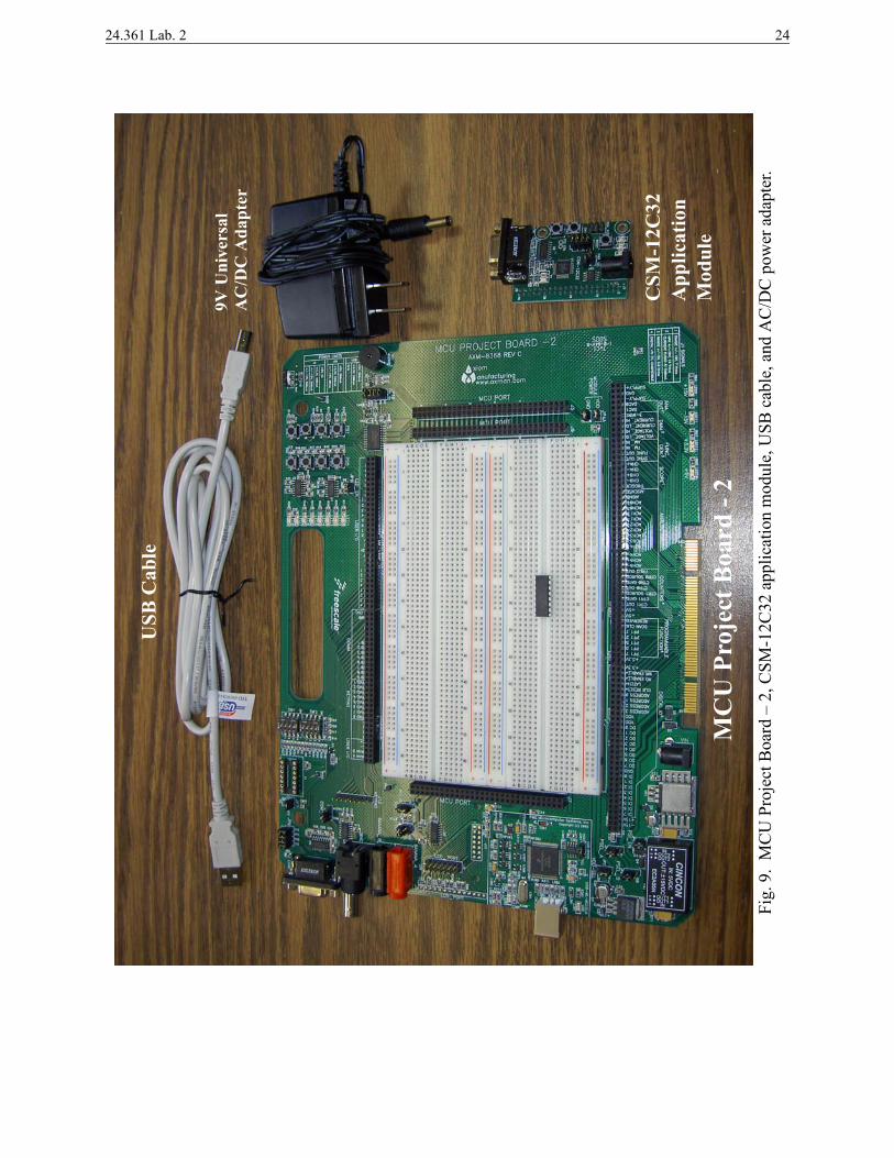
Ensure you have the following components, which comprise the development worksta-tion: A host PC, MCU Project Board - 2, CSM-12C32 MCU application module, USB cable, and+- 15V Universal AC/DC adapter (see Fig. 9).
2 BACKGROUND: INTRODUCTION TO THE DEVELOPMENT WORKSTATION
The development workstation consists of three main parts: a host computer (PC); a Uni-versal Serial Bus (USB) communications channel; the MCU Project Board - 2; and the CSM-12C32 MCU application module. In this lab, we primarily use the PC to develop our software.The USB serves as a communications medium, allowing us to upload, run, and debug our pro-grams on the CSM-12C32 MCU. The MCU Project Board - 2 contains circuits and devices whichare interfaced with the CSM-12C32 MCU. As well, there is a project board on which we can cre-ate, construct, and test prototype circuits and devices to interface with the CSM-12C32 MCU.
24.361 Lab. 2 11
3 SOFTWARE SETUP
We will be using the MetroWerks CodeWarrior Development Studio. This software has alreadybeen installed on the PC. Verify that it has been installed by running it.
1. StartProgramsFreescale CodeWarriorCodeWarrior Development Studio forS12(X) V5.1CodeWarrior IDE
2. If the program starts, then exit it: FileExit. Otherwise, contact the TA for help.
4 HARDWARE SETUP
NOTE: an antistatic wrist guard must be worn at all times when handling the boards. Failureto do so may result in expulsion from the lab and an incomplete mark for the course.
4.1 UNPACKING THE HARDWARE
1. Retrieve the MCU Project Board - 2 and CSM-12C32 from the storage desk and placethem on your workstation desk. Note: both boards should be inside their protectiveantistatic plastic bag. If they are not in their protective bag, do not touch them andimmediately contact the TA for help.
2. Attach one side of the antistatic wrist guard to the ground terminal of a power supplyand attach the other end to your wrist.
3. Unpack the boards and place them on a flat area of the workstation desk. Ensure suffi-cient space is available around the project board to safely construct and test prototypecircuits.
4. Inspect both the MCU Project Board – 2 and the CSM-12C32 application module forany obvious damage. If damage is found, contact the TA immediately for assistance.
5. Ensure you have the four items of equipment as shown in Fig. 9, i.e., MCU ProjectBoard – 2, CSM-12C32 application module, USB cable, and AC/DC power adapter.
4.2 CONFIGURING THE MCU PROJECT BOARD – 2
6. Verify that all the jumper settings are configured properly on the MCU Project Board –2 as shown by Fig. 1. Circles indicate the location on the project board where thejumpers are located. Jumpers in the “on” position are highlighted in color red.Connec-tions indicate the “on” or “installed” position of jumpers. For more informationregarding the funciton of these features, plase consult the document SLKS12QSG.

24.361 Lab. 2 12
Fig. 1. Jumper setting for the MCUSLK.

24.361 Lab. 2 13
4.3 CONFIGURING THE MC9S12C32 MCU APPLICATION MODULE
7. Verify that all the jumper settings are set as shown in Table 1. Jumpers in the “on”position are highlighted in color red. Connections indicate the “on” or “installed” posi-tion of jumpers. Ensure that jumpers are installed for only the highlighted pins: SW1,SW2, SW3_1 to SW3_4, LED1 to LED4, RV1, and RZ1. For more informationregarding the funciton of these features, plase consult the document SLKS12QSG..
8. If not installed already, install the MC9S12C32 MCU application module (CSM-12C32) in the MCU PORT connector J5 on the MCU Project Board - 2. Align pin 1 ofthe CSM-12C32 module with pin 1 of the MCU PORT connector J5 on the MCUProject Board - 2, as shown in Fig. 2.
Table 1: Summary of jumper settings for the CSM-12C32 for use with the Project Board.
Fig. 2. Installation of the MC9S12C32 MCU application module (CSM-12C32).

24.361 Lab. 2 14
4.4 CONNECTING THE HOST PC AND POWERING THE SYSTEM
9. Power up the Host PC and connect the USB cable to an available USB port on theHost PC. Note: the USB cable may already be connected to the Host PC.
10. Connect the other end of the USB cable to the USB connector of the MCU ProjectBoard - 2. The Host PC should verify that new hardware has been installed.
11. Verify that the green USB LED on the MCU Project Board – 2 is lit and the OrangeLED (near the USB connector) is lit.
12. Connect the AC/DC power adapter to the VIN barrel connector on the MCUSLK.
13. Verify that the +15 V LED, -15 V LED, +3.3 V LED, and +5 V LED on the MCUProject Board – 2 are lit.
14. Verify that the VDD LED on the MC9S12C32 MCU application module board(CSM12C32) is lit.
15. If the LEDs in Step 11 and Step 14 are not lit, contact the TA immediately for assist-ance.
16. The MCU Project Board – 2 and the MC9S12C32 MCU application module are nowready for use.
5 DEVELOPMENT USING METROWERKS CODE WARRIOR AND THE IDE
5.1 CREATING A PROJECT IN THE CODEWARRIOR ENVIRONMENT
After verifying the proper installation of the CodeWarrior development tools as described in theSection 3 Software Setup, and completing the MCU Project Board – 2 configuration as describedin Section 4 Hardware Setup, you can now begin to develop your application for the target micro-controller, CSM-12C32. This section will create and build a project under the CodeWarrior forHCS12 development tool platform.
1. Launch the CodeWarrior IDE by Selecting: StartProgramsFreescale CodeWarriorCodeWarrior Development Studio for S12(X) V5.1CodeWarrior IDE
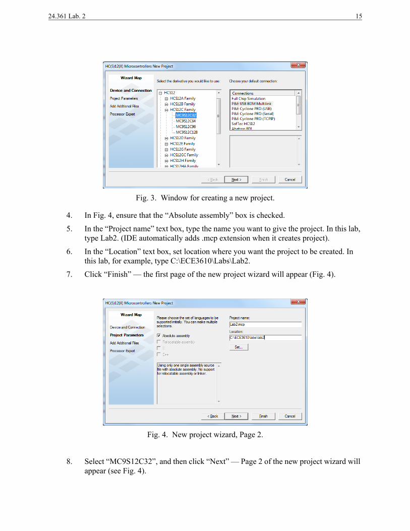
2. Create a new project: from IDE main menu bar, select: FileNew Project; a new window will appear (see Fig. 3).
3. Select: “HCS12C Family, and select P&E USB BDM Multilink, and then click Next.
24.361 Lab. 2 15
4. In Fig. 4, ensure that the “Absolute assembly” box is checked.
5. In the “Project name” text box, type the name you want to give the project. In this lab, type Lab2. (IDE automatically adds .mcp extension when it creates project).
6. In the “Location” text box, set location where you want the project to be created. In this lab, for example, type C:\ECE3610\Labs\Lab2.
7. Click “Finish” — the first page of the new project wizard will appear (Fig. 4).
8. Select “MC9S12C32”, and then click “Next” — Page 2 of the new project wizard will appear (see Fig. 4).
Fig. 3. Window for creating a new project.
Fig. 4. New project wizard, Page 2.

24.361 Lab. 2 16
5.2 BUILDING A PROJECT IN THE CODEWARRIOR ENVIRONMENT
Your project can contain multiple build targets. In this lab, we use the “P&E USB BDM Multi-link” target, which uses the USB BDM connector on the MCU Project Board – 2. This BDM con-nector provides bidirectional communication between the microcontroller and the debugger. It isalso possible to use the “Simulator” target. The “Simulator” target is useful when the hardware isnot available (outside of the ECE 3610 lab hours). When using the hardware, ensure the “P&EUSB BDM Multilink” target is selected.
5.2.1 TARGET SELECTION
1. Click the drop-down menu of the project window (see Fig. 5).
2. Select “P&E USB BDM Multilink” when the hardware is available.
3. Select “Simulator” when the hardware is unavailable.
5.2.2 EDIT SOURCE CODE
4. Click the “+” sign next to the “sources” folder to reveal files.
5. Double-click the main.asm file; an editor window will open and display the contents of main.asm.
6. Make changes to the contents of main.asm file, as shown in Fig. 6, by replacing the “CLI, MOVB #1,temp_byte, and NOP” instructions with the “LDAA $0800, ADDA $0801, and STAA $0802” instructions.
7. After you make changes to main.asm, from IDE main menu bar, select FileSave.
Target
Fig. 5. Project window. When using the MCU Project Board - 2 hardware, select “P&E USBBDM Multilink” as the target. When the hardware is not available, choose “Simulator”.
Specification

24.361 Lab. 2 17
5.2.3 BUILD PROJECT
8. From IDE main menu bar, select ProjectMake, or type F7. The IDE builds (assem-bles, compiles, and links) the project; The IDE translates your source code to machine code. If there are any errors or warnings, they will shown in a window.
5.3 RUNNING AND DEBUGGING AN APPLICATION IN THE CODEWARRIOR ENVIRONMENT
The following steps explain how to establish communication and upload your application soft-ware to the MC9S12C32 MCU application module (CSM-12C32). This will allow you to run aswell as debug your application through Metrowerks’ True-Time Simulator & Real-Time Debug-ger using the BDM pod interface on the MCU Project Board – 2.
5.3.1 START DEBUGGER
1. Click ProjectDebug, or type F5.
2. If the pop-up window (Fig. 7) appears, click on “Okay”. By clicking “Okay”, you are confirming that the machine code for your project should be written into the microcon-troller’s Flash memory. Check this box so that this message does not appear again.
3. The Debugger starts (Fig. 8) and opens several windows (Table 2).
Fig. 6. The main.asm file. The given instructions have been replaced with the LDAA $0800,ADDA $0801, STAA $0802, and BRA Entry instructions.

24.361 Lab. 2 18
Table 2: Debugger windows.
Window Name Description
Source and Assembly Displays application source code in C and assembly programming lan-guages, respectively
Register Displays the MCU internal registers
Memory Displays the active value at each memory address in the MCU internal memory map
Procedure Displays the active procedure being evaluated
Data 1 and Data 2 Display any global or local variables in your application software and their active value
Command Allows user control and logs commands executed
Fig. 7. Loader warning message. The loader wants verification that the Flash should be erasedand loaded with the machine code of your application.

24.361 Lab. 2 19
Fig
. 8.
The
deb
ugge
r/S
imul
ator
Win
dow
.

24.361 Lab. 2 20
5.3.2 RUNNING
To run your application at “full speed”:
4. Click RunStart, or type F5. This will run the instructions of your program at the full speed of the clock.
5.3.3 DEBUGGING
To debug your application, you can trace one instructions at a time or you can put a break point ata strategic location and then run full speed until the breakpoint is reached. For a full explanationof the tracing and debugging features of the IDE, see
HelpHelp TopicsIndexDebugging.
5.3.4 REGISTERS
You may view and modify the contents of the registers in the “Register” window. For a full expla-nation of the register modification features of the IDE, see:
HelpHelp topicsIndexRegister.
5.3.5 MEMORY
You may view and modify the contents of the memory in the “Memory” window. For a full expla-nation of the memory modification features, see:
HelpHelp topicsIndexMemory.
5.3.6 COMMAND
You may issue commands in the “Command” window. Type “help” in the command window toview all of the supported commands. For a full explanation of the commands features, see:
HelpHelp topicsIndexCommand, Syntax. Then choose “Simulator/Debugger Commands”.

24.361 Lab. 2 21
6 EXPERIMENT
6.1 READING FROM REGISTERS AND MEMORY LOCATIONS
Right click on the “LDAA $0800” instruction in the “Source” window, and select “Show Loca-tion”. The IDE will scroll the Memory window to show the contents of the memory where theinstruction is stored. Observe the values in the Memory window, and write down the machinecode for each instruction in Table 3. (Note: the memory could also be read by running a commandin the Command window, as shown in the following.)
Observe the Register window and take note of the register values for the PC, A, B, and NZVC ofthe CCR. Now perform a read of the registers by running the command in the Command window.Write down the syntax and command response of the register read command for each of the regis-ters in Table 4.
Scroll to locations $0800, $0801, and $0802 in the Memory window and take note of their values.Now perform a read of the memory at locations $0800, $0801, and $0802 by running the com-mand in the Command window. Write down the syntax and command response of the memoryread command for each of the memory locations in Table 4.
Table 3: Machine code for a simple routine.
Assembly Language
Machine Code (Hex)
LDAA $0800
ADDA $0801
STAA $0802
Table 4: Read Command Syntax for selected items.
Command Command Syntax Command Response
Read Register PC
Read Register A
Read Register B
Read Register CCR
Read Memory Location $0800
Read Memory Location $0801
Read Memory Location $0802
24.361 Lab. 2 22
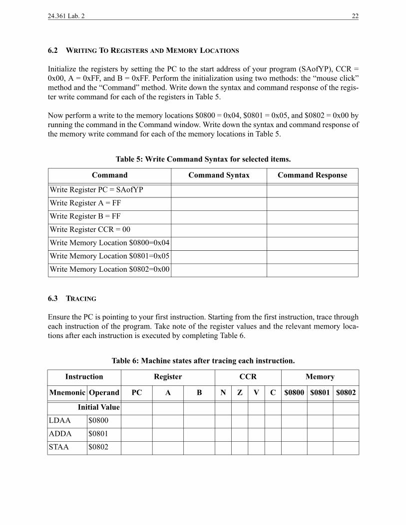
6.2 WRITING TO REGISTERS AND MEMORY LOCATIONS
Initialize the registers by setting the PC to the start address of your program (SAofYP), CCR =0x00, A = 0xFF, and B = 0xFF. Perform the initialization using two methods: the “mouse click”method and the “Command” method. Write down the syntax and command response of the regis-ter write command for each of the registers in Table 5.
Now perform a write to the memory locations $0800 = 0x04, $0801 = 0x05, and $0802 = 0x00 byrunning the command in the Command window. Write down the syntax and command response ofthe memory write command for each of the memory locations in Table 5.
6.3 TRACING
Ensure the PC is pointing to your first instruction. Starting from the first instruction, trace througheach instruction of the program. Take note of the register values and the relevant memory loca-tions after each instruction is executed by completing Table 6.
Table 5: Write Command Syntax for selected items.
Command Command Syntax Command Response
Write Register PC = SAofYP
Write Register A = FF
Write Register B = FF
Write Register CCR = 00
Write Memory Location $0800=0x04
Write Memory Location $0801=0x05
Write Memory Location $0802=0x00
Table 6: Machine states after tracing each instruction.
Instruction Register CCR Memory
Mnemonic Operand PC A B N Z V C $0800 $0801 $0802
Initial Value
LDAA $0800
ADDA $0801
STAA $0802
24.361 Lab. 2 23
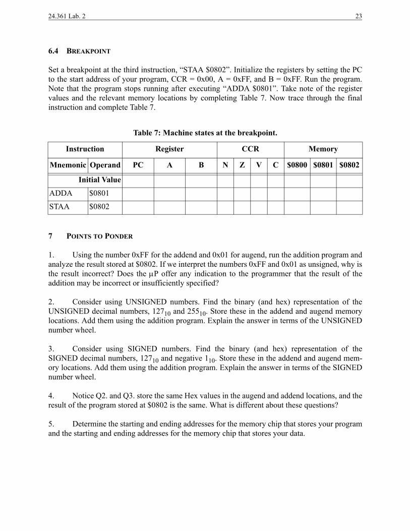
6.4 BREAKPOINT
Set a breakpoint at the third instruction, “STAA $0802”. Initialize the registers by setting the PCto the start address of your program, CCR = 0x00, A = 0xFF, and B = 0xFF. Run the program.Note that the program stops running after executing “ADDA $0801”. Take note of the registervalues and the relevant memory locations by completing Table 7. Now trace through the finalinstruction and complete Table 7.
7 POINTS TO PONDER
1. Using the number 0xFF for the addend and 0x01 for augend, run the addition program andanalyze the result stored at $0802. If we interpret the numbers 0xFF and 0x01 as unsigned, why isthe result incorrect? Does the P offer any indication to the programmer that the result of theaddition may be incorrect or insufficiently specified?
2. Consider using UNSIGNED numbers. Find the binary (and hex) representation of theUNSIGNED decimal numbers, 12710 and 25510. Store these in the addend and augend memorylocations. Add them using the addition program. Explain the answer in terms of the UNSIGNEDnumber wheel.
3. Consider using SIGNED numbers. Find the binary (and hex) representation of theSIGNED decimal numbers, 12710 and negative 110. Store these in the addend and augend mem-ory locations. Add them using the addition program. Explain the answer in terms of the SIGNEDnumber wheel.
4. Notice Q2. and Q3. store the same Hex values in the augend and addend locations, and theresult of the program stored at $0802 is the same. What is different about these questions?
5. Determine the starting and ending addresses for the memory chip that stores your programand the starting and ending addresses for the memory chip that stores your data.
Table 7: Machine states at the breakpoint.
Instruction Register CCR Memory
Mnemonic Operand PC A B N Z V C $0800 $0801 $0802
Initial Value
ADDA $0801
STAA $0802
24.361 Lab. 2 24
Fig
. 9.
MC
U P
roje
ct B
oard
– 2
, CS
M-1
2C32
app
lica
tion
mod
ule,
US
B c
able
, and
AC
/DC
pow
er a
dapt
er.
MC
U P
roje
ct B
oard
- 2
US
B C
able
9V U
niv
ersa
lA
C/D
C A
dap
ter
CS
M-1
2C32
Ap
pli
cati
onM
odu
le