Key Fob Design Based on Atmel ATA5795 - Microchip...
36
9224B-RKE-05/15 Features ● Integrated key fob solution integrating MCU and a passive transponder functionality using Fc = 125kHz for immobilizer applications via a contactless LF interface and an RF transmitter functionality with programmable Fc = 300MHz to 433MHz for RKE applications ● Transponder includes immobilizer SW stack supporting the immobilizer authentication protocol programmed at the factory ● Open source immobilizer SW stack Is based on flexible communication protocol. The protocol Is configurable using transponder configuration memory ● Immobilizer command set supports various classes of commands such as start authentication, read UID, read/write user memory, learn secret key1/2, and read transponder error status ● Integrated high speed AES-128 hardware crypto module ● Atmel ATA5795 includes segmented program and user data nonvolatile memories with protection locks ● Ultra low power consumption enables passive transponder functionality at low coupling factors (k < 0.8% typ.) ● Integrated RF transmitter module with selectable Fc using fractional PLL in ISM bands (315/430MHz) ● Configurable radiated power output pout at up to +12.5dBm ● Integrated flash-based Atmel ATmega 8-bit MCU includes ultra low-power design with many dedicated data communication and mixed-signal peripherals. Includes on-chip internal oscillators at 4MHz and 125kHz with RTC APPLICATION NOTE Key Fob Design Based on Atmel ATA5795 ATA5795
Transcript of Key Fob Design Based on Atmel ATA5795 - Microchip...

APPLICATION NOTE
Key Fob Design Based on Atmel ATA5795
ATA5795
Features
● Integrated key fob solution integrating MCU and a passive transponder
functionality using Fc = 125kHz for immobilizer applications via a contactless LF
interface and an RF transmitter functionality with programmable Fc = 300MHz to
433MHz for RKE applications
● Transponder includes immobilizer SW stack supporting the immobilizer
authentication protocol programmed at the factory
● Open source immobilizer SW stack Is based on flexible communication protocol.
The protocol Is configurable using transponder configuration memory
● Immobilizer command set supports various classes of commands such as start
authentication, read UID, read/write user memory, learn secret key1/2, and read
transponder error status
● Integrated high speed AES-128 hardware crypto module
● Atmel ATA5795 includes segmented program and user data nonvolatile memories
with protection locks
● Ultra low power consumption enables passive transponder functionality at low
coupling factors (k < 0.8% typ.)
● Integrated RF transmitter module with selectable Fc using fractional PLL in ISM
bands (315/430MHz)
● Configurable radiated power output pout at up to +12.5dBm
● Integrated flash-based Atmel ATmega 8-bit MCU includes ultra low-power design
with many dedicated data communication and mixed-signal peripherals. Includes
on-chip internal oscillators at 4MHz and 125kHz with RTC
9224B-RKE-05/15

1. Introduction
This application note introduces Atmel® ATA5795 as a building block to design a key fob with an integrated transponder and RKE functionality for the automotive industry.
It discusses the implementation of the key fob transponder, its physical interface, the hardware and software resources of the system and possible application scenarios. The open source Immobilizer Software Stack application code which is preprogrammed in the device program memory is also introduced and its features and configuration briefly discussed. The RKE functionality, features, and configuration relying on Atmel ATA5795 and application software are reviewed.
Atmel ATA5795 was designed to function as a transponder-based key fob using its contactless LF communication interface. It supports half-duplex LF data links with the base station. The base station generates the LF field. The data to the transponder is sent using On-Off keying. The data from the transponder is sent using ASK modulation by damping the carrier. The LF magnetic field is used as a data carrier and as a source of power to the transponder.
The RKE function consists of transmitting an RF data message to the vehicle for authentication. RKE message data is send via the RF link consisting of a transmitter unit ID and a cipher message. The link is active only for a few milliseconds to keep power dissipation low. The cipher is calculated using an AES-128 hardware-based crypto module.
Figure 1-1. Key Fob In-System Integration
1.1 Immobilizer Fob Application
The in-vehicle immobilizer system is primarily used for preventing engine starts by an unauthorized user. The system uses an LF field to communicate with the passive transponder. The communication is based on series of unidirectional data transfers between the base station (vehicle) and the transponder (key fob).
The immobilizer system includes:
1. Body Control Module (BCM): It is connected directly to the engine control module and is used as an authentica-tion unit to enable engine start. It issues challenges and evaluates responses from the key to enable or disable access.
2. Base Station (BS): This module acts as a gateway between the key fob and the BCM. It communicates with the key via its physical interface.
3. Transponder (TP): The transponder unit receives data from the base station including commands and payload data and responds accordingly. Its internally stored secret key (128 bits) is used to encrypt challenges before it replies with a response prior to authentication.
LF DataLink
VBAT
Key Fob IC(ATA5795)
LF BaseStation
Immobilizer FunctionLF Energy
RFReceiver
RKE Function
KeyVehicle
RF DataLink
CVDD
BodyControlModule(BCM)
AccessControlModule
Vehicle ECU
SPI, SSI
LIN,SPI
Pushbuttonswitches
ATA5795 [APPLICATION NOTE]9224B–RKE–05/15
2

Figure 1-2. Immobilizer System Diagram
The transponder can receive modulated data from the base station (downlink) and transmit data back to the base station (uplink).
The authentication protocol is based on challenge response topology and it can be implemented either as a unidirectional protocol where only a key is authenticated by the vehicle or as a bidirectional protocol where a key and a vehicle are both authenticated. Varying data frame sizes may be used to send and receive payload data. Plain text challenge data received by the fob is encrypted by the AES-128 hardware-based crypto module, after which the cipher response is sent to the base station.
The energy to receive and transmit the protocol data is supplied by the magnetic field which is directly coupled from the base station coil to the transponder coil during the data exchange. The transponder can also be powered by an internal battery. This feature is used for fob configuration and during key fob debug and development.
1.2 RKE Fob Application
RKE functionality is achieved by transmitting authentication data from the key fob to the vehicle via a unidirectional RF data link. Normally this function is used for remote communication with the vehicle via the RF link by physically interfacing with the key fob (e.g., pushing the button).
Important key fob RKE features include:
● Integrated RKE Data Transmitter (RF Uplink): ASK/FSK 300-450MHz, 40kBaud transmitter with high power output (+12dBm)
● Generation of Soft Configurable Secure Protocols: Authentication is based on a rolling code protocol. The message text is ciphered using a built-in AES-128 cryptographic engine.
● Low Power Consumption: A large selection of sleep modes. Multi-source system clock.
1.3 Fob Application Circuit
The Atmel® ATA5795 was designed for low cost applications and requires a minimal number of external components. The simplified schematic diagram shown below depicts a typical application components design for 433MHz. The reference design is shown in Appendix A.
The diagram includes the LF link coil L1 and the capacitor CL1 as the transponder antenna for immobilizer applications (fosc = 125kHz). Matching L1, CL values produce large Q which improves data integrity and immobilizer range.
The RF link loop antenna is shown to be driven by the PA (pin 28) with its return path on pin 27 which is also the ground. Capacitors C7, C8 and C10 and inductor L3 were selected to match the antenna impedance for best power output. Their values were also based on actual trace impedance of the reference PCB. C4 and L2 on the other hand are used as a supply block against PA noise which could couple into the power supply and disturb the PLL circuit. Both should be placed close to pin 28. Additionally L2 provides for the antenna bias.
RF loop antenna traces during layout should not exceed 1.5mm to keep antenna Q from reaching excessive values. For 13MHz Xtal, load capacitors C5 and C6 must be selected for XTO to run on the load resonance frequency of the crystal.
Main controller indashboard Basestation
Key withTransponder
LF-communicationprotocol for
authentication
Datacommunication
Data communication(command set, data
handling), authentication,AES encryption
LF-communication (up-and downlink), LF-
command interpreter,AES encryption
TP BS BCM
downlinkuplink
Transparent communicationwith BCM,
LF-communication with TP(write and read of transponder
data)
3ATA5795 [APPLICATION NOTE]9224B–RKE–05/15

The In-System Programming (ISP) connection is shown as pin 24 (MISO), 25 (MOSI), 26 (SCK). The serial ISP connector pins as provided on the 6-pin ISP header are:
Pin 1: MISO Pin 6: VBAT
Pin 2: SCK Pin 5: MOSI
Pin 3: NReset Pin 4: GND
The supply Vbat is typically delivered from a single Li cell battery.
Figure 1-3. Application Circuit
Table 1-1. Components Selected for RF Fc = 433.92MHz
Symbol Value Description
L1 2.35mH TP coil inductor
CL1 680pF TP coil LC tank capacitor
C2 68nF VBref decoupling capacitor
C5, C6 15pF 13MHz Xtal
C7 3.9pF Loop antennal impedance match capacitor
C8 3.4pF Loop antennal impedance match capacitor
C10 1.26pF Loop antennal impedance match capacitor
L2 27nH PA supply voltage decoupling
C4 1nF PA supply voltage decoupling
L3 12nH Antenna coupling inductor
CBUF
1617
18
19
20
21
22
23
24
8
7
6
5
4
3
2
1
15 14 13
AtmelATA5795
12 11 10 9
25 26 27 28 29 30 31 32
TP Coil
AVR MCU
VBATBattery
Base Station:ATA5272
Key Vehicle
LF link
RF linkRF- Receiver
ATA574xATA572xATA5780
ECU-1
ECU-2
C2
NRESET
C5
Q1 =13.5MHz
L1
CL1
C3
*ISP-pin
Q2 = 32.768kHz
L2
C7 C6
C4
C10RF-
Loop antennaC8
L3
*ISP-interface
ATA5795 [APPLICATION NOTE]9224B–RKE–05/15
4

2. Application Software
Application software is partitioned into two dedicated software modules, with each placed in its dedicated program memory address space:
● Immobilizer SW Stack Module: This firmware fully supports LF channel communication with the base station. Its features include:
● Controls LF link communication with the base station via an LF field. It includes device drivers and application modules that control the protocol handler.
● Provides for system, user, and application command support. Specific configuration commands can set transponder configuration including transponder crypto keys, set the modulation type used for up and down links, and set the baud rate and many other parameters. Other application level commands control unidirectional and bidirectional execution.
● A configuration file which controls transponder functionality. By programming configuration file parameters a user can select desired functional and performance features for the software (e.g., select authentication type, enable detection header, set modulation type for up and down channel and the baud rate).
● Factory preprogrammed image resident in the boot sector (address 0xC00 - 0xFFF). The section is individually protected with its own lock fuses.
● RKE SW Module: This firmware controls the user interface and RF transmitter. Its features include:
● Assembly and transmission of authentication messages to a vehicle based on unidirectional rolling code protocol
● Resident in application memory section (address: 0x000 - 0xBFF)
● Controls a flexible user interface using pin-change interrupts
● Incorporates configurable physical and application parameters:
● Physical layer parameters:
- Selectable RF carrier frequency (300MHz to 450MHz)
- Selectable modulation type (ASK versus FSK)
- Selectable radiated RF output power● Application layer parameters:
- Preamble signaling
- Definition of communication protocol and authentication type
- Payload data size (UID, CMD, CNTR, data padding)
2.1 Key Fob Firmware Overview
The key fob can either operate as an RKE transmitter or a secure transponder. The program memory is thus partitioned into two separate program sections: (1) the immobilizer section which controls the immobilizer functionality and (2) the application section which supports RKE and extra features.
With preprogrammed immobilizer SW stack the device always vectors to the boot section of the program memory which contains the dedicated firmware used to communicate with the immobilizer system on device reset. Upon reset the immobilizer SW stack must check if the LF field is available. When detected the software control remains in the immobilizer module and if not it is vectored to the application section.
The device is said to be in the RKE operating mode when the LF field has not been detected at device reset and the program control has been passed to the application code section. In this mode the key fob can send RF telegrams to the vehicle using its RF transmitter while powered by the internal battery voltage, VBAT.
The device is said to be in the immobilizer operating mode when the LF field has been detected and the device triggers internal reset which vectors its program control to the boot sector of the program memory, where the immobilizer specific firmware is executed. In normal operation, upon completion of the immobilizer protocol while the LF field is disabled the device triggers its internal reset and, with no LF field detected, it vectors from the reset vector to the application section to enter RKE mode.
5ATA5795 [APPLICATION NOTE]9224B–RKE–05/15

Figure 2-1. Program Memory Partitioning
2.1.1 Passive Operation in Immobilizer Mode
The device enters the transponder mode regardless of its current operating state (RKE, power-down) when the LF field is detected (i.e., the transponder mode supersedes any other device state).
Once the transponder mode is active the device power is set to VCC (the passive voltage stored on the charge storage capacitor CVDD which has been harvested from the field). Then the device can receive and transmit data in passive mode via the LF link.
When the LF field is removed and a battery is present, the transponder executes a system reset, checks if LF field is present and, if it is not detected, re-enters RKE mode. Then the device is reinitialized for RKE operating mode and a new outgoing RF message is assembled in its data memory.
When no battery or a low battery voltage level is detected on the VBAT pin, the transponder can still use emergency mode to enter the immobilizer passive mode and respond to the base station commands with the LF field present.
The diagram below depicts a power-up process and a mode changing sequence based on the presence of the LF field while being powered by the external battery. With no LF field present the device enters RKE mode when the battery voltage is provided at the VBAT pin. The device will exit RKE mode and automatically enter immobilizer mode when the LF field is detected. The device stays in immobilizer mode as long as the LF field is provided. When the field is removed the device returns to RKE mode.
Similarly, in emergency operating mode the device enters the transponder mode from power-down when the LF field is detected and leaves the transponder mode when the field is removed.
Address 0 15
0x0000
0x0BFF
0x0C00
0x0FFF 4095
3072
3071
0
Appl
icat
ion
Spac
e(3
072
Wor
ds)
Imm
obili
zer
Spa
ce(1
024
Wor
ds)
ATA5795 [APPLICATION NOTE]9224B–RKE–05/15
6
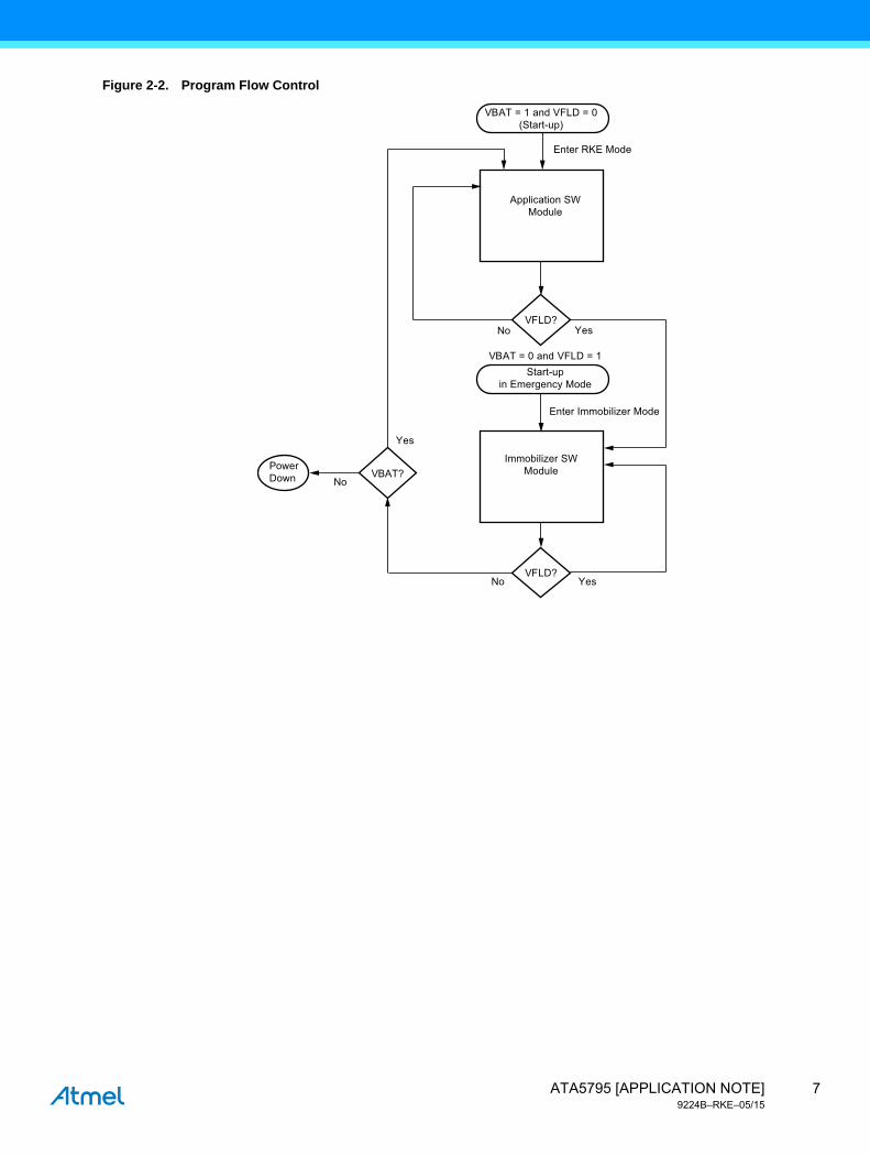
Figure 2-2. Program Flow Control
VBAT = 1 and VFLD = 0(Start-up)
Application SWModule
Immobilizer SWModule
VBAT = 0 and VFLD = 1Start-up
in Emergency Mode
Enter RKE Mode
Enter Immobilizer Mode
VFLD?No
Yes No
No
Yes
Yes
PowerDown
VFLD?
VBAT?
7ATA5795 [APPLICATION NOTE]9224B–RKE–05/15

3. Transponder Operation
Transponder operation is based on establishing an LF data link between the transponder and the base station and receiving, executing, and replying to a series of communication commands sent by the base station using the LF field.
3.1 Immobilizer Software Stack Overview
Atmel® ATA5795 is delivered with a preprogrammed Immobilizer Software Stack image; see [2] for the full functional specification. This open source firmware supports full key fob transponder behavior.
Software features:
● Supports Atmel ATA5795 device physical LF interface, power management, and other hardware resources
● Defined LF data links
● Defined command set
● Defined and reconfigurable protocols
● Programmable configuration settings
The stack physical drivers control the device hardware. Its application layer controls the command interface and execution. A command interpreter and protocol handler engine provide a transaction and system extraction layer when communicating with the base station.
Various communication protocols, data length, modulation types, baud rates, and transponder behavior can be set by changing the configuration file placed in the device EEPROM.
3.1.1 Software Stack Command Set
The base station - transponder communication is based on the command-response topology in which a base station (communication master) issues individual requests (commands) to a transponder, the communication slave, and the transponder generates corresponding replies (responses).
The command set is structured in a way that every command issued generates a transponder reply. The transponder interprets and executes commands based on its preprogrammed configuration file in its non-volatile memory (EEPROM). Commands include (1) utility requests, such as reading the device ID and reading from/writing to user memory, (2) authentication requests which start an authentication protocol execution, (3) diagnostics which query the transponder status and (4) key learn (sharing the secret key) commands that trigger key learn routines.
Some commands (i.e., authentication requests) may involve multiple data exchanges between the base station and the transponder. However, most commands are structured so that the transponder receives individual commands which may be followed by a data payload and a response. For example, to start an authentication sequence, the base station can first issue a Read_UID command and then after receiving the correct UID can follow up with a Start_Authentication command.
ATA5795 [APPLICATION NOTE]9224B–RKE–05/15
8

3.1.2 Command Execution
Once the LF link is established the commands are received on the downlink and the response data is sent on the uplink. Upon receiving data the transponder first validates received data (CRC-4 for commands, CRC-8 for payload data), decodes command data, executes a command by first generating response data, tests packet data integrity (CRC-8), encodes and transmits data via the uplink. When the transponder cannot validate and interpret the received data it signals the error to the base station (i.e., sends four periods of 1kHz).
The transponder must always reply to any base station command request. When the base station does not receive any reply within its reply time window, it resends its request until the number of maximum retries is reached.
Figure 3-1. Immobilizer Command Execution
The LF data link is aborted by the base station when the LF field is disabled.
The LF data link is terminated by the base station when:
● The protocol session is completed (the LF field is disabled)
● The base station received an error signal from the transponder and further diagnostics continue returning the error signal (timeout has been reached, the LF field is disabled)
● The base station receives a command from BCM to disable the LF field
Yes
Fld Present?No
Start(VDD = VBAT or VDD = 0)
Yes
No
Execute Reset Vector
Initialize peripherals
Enter Sleep
GAP?
Receive Command
Transmit Response
Data Valid?No
Yes
Execute Command
Flag Error
2
2
2
9ATA5795 [APPLICATION NOTE]9224B–RKE–05/15

3.1.3 Transponder Configuration File
Initially the transponder is configured by programming its EEPROM configuration memory. The transponder secret keys must be directly programmed during configuration using dedicated configuration memory commands.
Transponder device settings are stored in EEPROM page 1 and page 2 user data memory. Page 2 contains read-only configuration parameters (data cannot be overwritten) and page 1 contains data protected with software and hardware locks [2] which can be reconfigured using configuration commands.
Parameters flashed to the configuration memory in EEPROM page 2 include:
● User and transponder data settings
● Default secret key (SK0-SK119)
● Challenge, response length
● Unique ID/serial #
● Configuration register
● Crypto Mode (CM): bilateral, unilateral
● Data Check Disable (DCD)
● Uplink Modulation (MOD) - Bi-phase/Manchester
● Downlink Coding (DLP{1:0])
● Key Select (KS)
● Secure Key Transfer (SKT)
● Fob power-up
● BPLM, QPLM decoder threshold
● Transponder damping level
● Charge pump selection
● WDT timeout (Watchdog timer register)
3.1.4 Authentication Sequences
The execution of authentication sequences is initiated upon reception of the Start_Authentication command. Once the command is received, the CM bit in the configuration register determines the UA or BA authentication type and Challenge_Length and Response_Length registers set challenge and response bit lengths respectively.
An example of a Unilateral Authentication (UA) sequence is shown in Figure 3-2 on page 11.
ATA5795 [APPLICATION NOTE]9224B–RKE–05/15
10

Figure 3-2. Unilateral Authentication Protocol
3.1.5 Immobilizer Command Summary
The base station and the transponder communicate with each other via the LF downlinks and uplinks. The commands sent by the base station cover a large functional domain and include commands to read device ID, start authentication sequence, start key learn procedures, read status, and execute utility commands (Table 3-1).
Authentication UA1
Downlink = 124 bits = 31.7ms/47.6msUplink = 120 bits = 30.7msTotal = 78.3ms just LF bits worst case
AES-128 (enc.)
Response
AES-128 (enc.)
Response
Challenge
Random number
ID
Read UIDKey
memory
Challenge
IDKey
memory
Keymemory
Key Car
= STOP
VALID
8 + 56 + 8 bit
8 + 100 + 8 bit
8 + 32 + 8 bit
8 + 0 bit
Detection Header
LF Field ON
OK, it is theright key
YN
Start AuthenticationCmd
Read UIDCmd
Table 3-1. Immobilizer Commands Overview
Command Class Description Notes
Read UID Reads unique transponder ID from EEPROMBase station usually inquires for the transponder ID at the beginning of the authentication sequence.
Read Error Status Reads transponder status byteIn case the base station detects an error condition (e.g. missing or incorrect data)
Start AuthenticationStarts transponder authentication sequence based on configuration stored in transponder EEPROM
Transponder reads its configuration memory to execute this command (authentication type, bit no., key, etc.)
Learn Secret Key1/2Starts transponder Secret Key1 or Key2 learning sequence
Transponder reads its configuration memory to execute this command (learn sequence type, key, etc.)
Initiate Enhanced Mode
Sets transponder to enhanced modeEnhanced mode is used to configure transponder EEPROM while powered by an external battery
Repeat Last Response Request to transponder to resend the last response Used in retry strategy scenarios
Read User MemoryReads a section of user memory placed in transponder EEPROM
EEPROM address and data size is sent with the command
Write User MemoryWrites a section of user memory into transponder EEPROM
EEPROM address and data size is sent with the command
Write Memory Access Protection
Writes transponder user memory access protection for AP1, AP2, and AP3 sections.
Protects user memory against accidental data overwrite
11ATA5795 [APPLICATION NOTE]9224B–RKE–05/15

3.2 LF Link Overview● Downlink (base station to transponder unidirectional communication)
● ASK modulation (VFLD can vary depending on modulation depth from VFLD undamped level down to ground)
● BPLM, QPLM data encoding
● BPLM data rate up to 5.2kBaud (BPLMD0 -> Tbit = 12 Tc + 12 Tc = 192µs,
● QPLM data rate up to 8.9kBaud (QPLMD00 -> 2Tbit = 12 Tc + 16 Tc = 224µs)
● Uplink (transponder to base station unidirectional communication)
● ASK modulation (Vdamped, Vundamped)
● Manchester, bi-phase encoding
● Variable modulation depth available
● Data rate up to 5.2kBaud (Tbit = 2 12Tc = 192µs)
3.2.1 LF Link Data Communication Protocol
The example below depicts a sample of a unilateral authentication data communication sequence with the base station:
1. At startup the transponder coil is energized for approx. 2ms and the transponder signal validated for another 2ms.
2. Once validation is successful Cvdd is charged for approx. 2ms. At this time the transponder mode is acknowledged and the transponder replies by sending its detection header.
3. The base station transmits its 4-bit command followed by a 4-bit CRC value.
4. The transponder receives the command and replies with a preamble followed by its 32-bit device ID.
5. The base station sends a challenge followed by its CRC-8 value.
6. The transponder encrypts the challenge using its internal AES-128 secret key.
7. The transponder responds by sending the cipher data to the base station.
Figure 3-3. Immobilizer Protocol Example
Field on, receiver active
Transponderdetectionheader
4-bit command + 4-bit CRC
8-bit preamble + 32-bit of key + 8-bit CRC
100/120-bit challenge + 8-bit CRC
8-bit preamble + 56-bit response + 8-bit CRC
LF fieldconnection
C bufferchange
BS
BS
TP
Mag. field
Start up
During Stop condition switch to receiveand wait for ID
Transponder detected, sendGap in damped phase,
transmit command
Read ID from EEPROM and send to BSPower up and switchto transponder mode
With first gap stop modulatingand receive command
Transmit challenge Receive responseSwitch toreceive
Receive the challenge plain text Return encrypted responseEncrypt(AES)
ATA5795 [APPLICATION NOTE]9224B–RKE–05/15
12

3.3 Configuring and Operating the Transponder
The device is configured by the reset vector (i.e., POR is triggered) on power-up. The device may be powered in two different ways:
1. VBAT: A battery is inserted between the VBAT and GND terminals. When powered initially by a battery with no VFLD voltage detected, the device is configured in RKE mode: (1) the device checks if VFLD is detected, (2) if VFLD=0, an RKE message data is assembled in data memory, (3) the device enters sleep mode to be awakened by a pin-change interrupt to transmit the RKE data on the RF channel.
2. VFLD: The device is placed in the LF field and VFLD voltage is detected at its coil inputs. VCC is ramped from 0 to its nominal operating potential. When powered in this mode the device is configured as a transponder to execute LF link commands (i.e., to receive LF data in transponder mode to support execution of LF downlink commands).
Figure 3-4. Device Initialization
3.3.1 Devices Utilizing Immobilizer Stack
By setting Interrupt Vector Select bit (IVSEL) to one and RESET fuse set to vector to immobilizer code section on reset, both the interrupt vector table and the reset start program counter address are moved to the boot space memory. This facilitates execution of the field voltage check and transponder initialization from the boot sector memory on power-up. Once VFLD check is executed the program control remains either in the immobilizer code section if VFLD is detected or is passed to the RKE application code (see Figure 3-4 above).
3.3.2 Transponder Initialization
The transponder LF communication is enabled only in transponder mode.
Normally when the LF field is detected and the LF signal is qualified to be the valid LF field source, the setup power-up condition must be satisfied to qualify a valid transponder signal (i.e. Tsetup = ~3ms, Ttp = 1ms, Tcharge = 1ms).
Only after this validation, a reset is generated and the VDD source can be switched from VBAT to VFLD to support the passive mode of operation.
Once the transponder mode is acknowledged the LF link is established.
Yes VFLD?
No
Device Power-up(VBAT or VFLD)
Enter RKE Mode Enter TP Mode
Init LF-link
Assemble RKE Msg. Wait for TPGAP
Execute LF-link command/protocol
Transmit RKE Message
Enter SleepWait for Key Push
Init LF-link
13ATA5795 [APPLICATION NOTE]9224B–RKE–05/15

3.3.3 Power Modes
The transponder can be operated either as a passive or an active device. The Transponder Power Supply Disable bit (TPPSD) in the TPCR register controls the source of device power supply during initialization at power-up.
The device is set to passive mode when TPPSD=0 (default) in the TPCR register during initialization. Once this bit is read by the internal transponder logic at the initialization phase the device will remain in passive mode until the device leaves the transponder mode (e.g., the field voltage is removed or device reset is triggered).
During the reset vector routine, the transponder mode must be acknowledged while in passive operation. The transponder mode must be acknowledged while in active operation (VDD=VBAT) by using Transponder Mode Interrupt TPINT.
See Table 3-2 for more details.
Note: With the power switching disabled Atmel® ATA5795 does not generate a reset when entering transponder mode. The transponder continues to be supplied by battery voltage and continues its normal program execution.
3.4 Immobilizer Performance
The immobilizer system coupling factor has a determining effect on the immobilizer performance as a whole. The coupling factor is influenced by many parameters which consist of a base station transceiver IC with coil, the transponder unit with coil, and their operating physical environment (e.g. ignition lock casing material, transponder setting and its material, distance between coils, coil size, coil material, Q factors, etc.).
3.4.1 Magnetic Coupling
By definition the coupling factor k is a magnetic field coil-to-coil coupling parameter depending, among many other factors, on many physical and electrical parameters such as the reader and transponder coils dimensions, inductance, coils orientation with respect to each other and the distance between them. Larger cross-section iron core transponder coils improve magnetic coupling and extend operating range. Their large Q factors when correctly tuned to the base station carrier frequency can greatly extend key fob operating range. The base station load current and the supply voltage amplitude can also increase the magnetic field generated by the base station coil.
In RFID systems the coupling factor can be determined by measuring the voltage of the reader and transponder coil. A basic coupling factor can be measured by measuring transponder coil voltage Vtp with its oscillating tank capacitor and transponder removed (see Formula 1 below).
Formula 1
Table 3-2. Active versus Passive Mode
Characteristic Active Mode (TPPSD=1) Passive Mode (TPPSD=0)
VDD switching(1) disabled(2) enabled
Reset upon entering transponder mode No Yes
Transponder Active (TPA bit in TPFR) TPA=1 TPA=1
TP IRQ Enabled Disabled
Acknowledge TP Mode TPINT interrupt(3) Reset Vector (at init)
DebugWIRE Enabled Enabled(4)
IO ports Enabled Disabled
Notes: 1. Device can switch its power source when entering transponder operating mode based on TPPSD bit setting
2. Must assert TPSSD to disable VDD switching
3. No reset is generated when entering transponder operating mode during active operation
4. External power supply must be provided to VBAT pin in passive mode
kVTag
VReader-----------------
LReader
LTag-----------------
ATA5795 [APPLICATION NOTE]9224B–RKE–05/15
14

● k: coupling factor
● VTag: transponder voltage
● VReader: reader voltage
● LReader: reader inductance
● LTag: transponder inductance
Transponder parasitic loading effects on the coupling can be included in the coupling calculation according to the circuit shown in Figure 3-5. Formula 2 can also be used to incorporate transponder loading effects of the transponder coil. The loading normally includes a resistive current load and a parasitic capacitance.
Formula 2
A parasitic loading constant Ak is dependent on the parasitic load values of a transponder. Its value for a typical coil and the transponder input is determined as Ak = 0.92 for a capacitive load of approx. 10-12pF.
Figure 3-5. Coupling Factor Measurement Circuit
The chart below shows a transponder-to-reader coupling variance for a set of measurements. Four base station/transponder coil combinations were used. Base station coils consist of (1) 40mm Rehfeld with L = 646µH coil and (2) 80mm Tranex with L = 738µH coils. The two transponder coils include (1) Kaschke/L = 2.45mH and (2) TR1103/L = 5.1mH coils; both use ferrite cores. With the best coupling measured directly at the base station coil center (d = 0cm), for every coil combination the coupling factor k drops rapidly to approximately k = 1% at a distance of ~4cm. The coupling drops more gradually as the distance from the base station coil increases.
k Ak
VTag
VReader-----------------
LReader
LTag-----------------
Reader Antenna Coil Transponder Antenna Coil
LTP
RPAR
CPARVTP
+
-
LRD
RRD
CRD
k
Coil1
Coil2
Input Demod
15ATA5795 [APPLICATION NOTE]9224B–RKE–05/15

Figure 3-6. Measured Coupling Factors for Immobilizer System
3.4.2 Minimum Coupling Factor
A minimum coupling factor kmin specified for an immobilizer can be used as a system performance parameter. As it is primarily based on immobilizer system electrical and physical characteristics, it is also an indicator of the transponder performance. To measure a minimum coupling factor a series of communication rounds were executed for a fixed set of system parameters which include coil types, reader coil current, and a transponder environment. The transponder coil was placed at various distances from the reader coil while executing the immobilizer communication sequence. The minimum coupling was calculated at the most distant point from the reader with the functional communication link. The transponder and the reader coil voltages were measured at the farthest distance from the reader coil with the transponder and the tank capacitor disconnected (see Figure 3-5 on page 15). The coupling factor for open and loaded transponder oscillator tank can be calculated using Formula 1 and Formula 2 respectively. Sample measurements of the minimum coupling factor for some coil combinations are listed in Table 3-3.
3.4.3 Data Link Quality
One of the factors which increases energy and data coupling performance for a contactless passive transponder is to increase antenna quality factors Q as indicated in the formula below.
Formula 3
Transponder antenna Q can be increased by using larger ferrite core-based coils. By tuning the transponder oscillating circuit to within 1-2% of base station Fc, much greater VTag voltages can also be induced.
0 0.02 0.04 0.06 0.08 0.1
Distance d (m)
7
6
5
4
3
8
2
1
0
Cou
plin
g Fa
ctor
(%)
9
Lr = Rehfeld, Lt = 2.45mHLr =Rehfeld, Lt = 5.1mHLr = 738μH, Lt = 2.45mHLr = 738μH, Lt = 5.1mH
Table 3-3. Minimum Coupling Factors for Atmel ATA5795(1)
RD Coil TP Coil V_RD [V] V_TP [V]Operating
Range [cm]Kmin (open)(2)
[%]Kmin (loaded)(3)
[%]
Wagner (L = 745µH)
Premo TR1102 (2.38mH)
120.3 2.06 2.9 0.96 0.88
Wagner (L = 745µH)
Kaschke (2.34mH)
113.7 1.68 3.6 0.83 0.76
Notes: 1. The transponder consists of the Atmel ATA5795 device programmed with Open Source License AES-128 Immobilizer Protocol Stack firmware executing BA authentication protocol
2. Minimum coupling does not include load parasitics
3. Minimum coupling includes load parasitics
Qcoil
XL
R------- Im Z
Re Z -----------------= =
ATA5795 [APPLICATION NOTE]9224B–RKE–05/15
16

The reader coil Q factor is not only dependent on coil inductance but also on its coil's loss resistance and iron losses of the coil when it is mounted on a lock cylinder. Inserting a series resistor into the antenna coil circuit makes the coil circuit more resilient and reduces negative effects of the lock cylinder material. Reader coils with high Q values improve energy transmission but their transient response may have a negative effect on the data signal quality. It is generally recommended that Q factors of no more than 15 be used in the reader coil designs. Medium Q values provide a good tradeoff between acceptable energy coupling and good data integrity between the reader and the transponder units.
3.4.4 Modulation Depth
To extend transponder operating range for uplink communication, Atmel® ATA5795 modulation depth level can be increased by setting transponder modulation depth bits from their default setting TPMD=00 to TPMS=01.
3.5 Transponder Communication Examples
The chart below depicts a captured challenge response protocol signaling in passive mode. The transponder coil voltage V4P is shown in green and VCC charge storage capacitor is shown as a yellow trace. Upon transponder startup, the VCC charges rapidly and the challenge 128-bit BPLM modulated data is sent after 10ms. The transponder receives the data, encrypts it and responds with a 128-bit response (50% modulation depth).
Figure 3-7. Immobilizer Challenge Response Scope Trace
Figure 3-8. Transponder Startup Timing and BPLM Data Encoding Using Downlink
17ATA5795 [APPLICATION NOTE]9224B–RKE–05/15

4. Remote Keyless Entry Operation
Main RKE functionality:
● Secure authentication cipher based protocol
● Physical user interface includes push button controls
● Flexible RF link frequency in 315MHz to 430MHz ISM band
4.1 RKE Fob Control
The top-level RKE module software architecture block diagram below depicts main functional steps while the device is in the RKE mode.
RKE mode setup and operation overview sequence of events:
1. The battery is inserted and the reset is triggered (POR)
2. The fob is initialized
3. The RKE message is assembled and stored in data memory
4. Sleep mode is activated (device enters power-save mode)
5. Push button event triggers an MCU wake-up event
6. Wake-up event is decoded
7. Event decoded command is selected
8. RF transmitter is enabled and configured
9. The RKE message is transmitted
10. Upon message transmission the unit assembles a new message and enters power-save sleep mode
Figure 4-1. RKE Mode Flow Diagram
Insert Battery
Fob Init
Enter Sleep
Transmit Msg.
Configure RF Transmitter
LF Field Execute IMMO Code
Push Button (Pin Change IRQ)
Decode UI Command
Assemble RKE Msg.LF Field
LF Field
LF Field
LF Field
LF Field
RESET
ATA5795 [APPLICATION NOTE]9224B–RKE–05/15
18

4.2 Physical User Interface
The programmable UI used in RKE mode which is based on any physical external triggers may include push buttons or touch sensors or other stimulus to communicate external events to the key fob MCU.
There are a total of 16 GPIO pins capable of generating pin-change interrupts to the MCU.
Note: Device GPIO pins are only enabled in RKE operating mode. All GPIO pins are disabled in passive transponder operating mode.
4.3 RF Link Implementation
The RF uplink is established at the selected carrier frequency (Fc) using either ASK or FSK modulation. The message data which includes a vehicle command and an authentication data is assembled by the RKE application software module and is sent via the RF uplink as a unidirectional data transfer.
4.3.1 RF Communication Protocol
The protocol is based on a unidirectional RF link which is transmitted from the key fob to the vehicle. It incorporates a secure rolling code algorithm where each message is unique in a sense that it includes an incrementing (rolling) counter value. Each message consists of the following:
● Unique ID
● Command code
● Counter value code
● Message Authentication Code (MAC)
● Data integrity CRC-8 code
4.3.2 RKE Message Generation
When generating RKE message data the following must be considered:
● Protocol security:
● Message uniqueness
● Integrated MAC based on AES-128 cipher algorithm
● Power consumption
Each key fob must be uniquely identified using its unique ID number. The (32-bit) UID value is transmitted in the message to identify a key fob/vehicle match.
The key fob must also be able to send system commands to the vehicle. A command set based on 8-bit values in the command field is sufficient for most applications.
The issue of protocol security deals with a system's immunity to scan or dictionary attacks. Scan attacks target the transmission of a high volume of data and simply scan the contents for values in the payload until the right code is accepted. A dictionary attack is based on storing part of the code and predicting the rest of the message (looking it up in the dictionary of codes) based on stored dictionary results of previously captured combinations from the real authentication sequences.
A rolling counter algorithm shows a high degree of immunity to existing protocol attacks. This algorithm is based on using an incrementing binary value which is encapsulated in the MAC frame. Each time a new outgoing message is transmitted a new MAC frame is calculated based on the new counter value.
When selecting the size for the sequential counter the window of acceptance values selected by the receiver must be considered. Normally this window must be a small fraction of the full counter range so when the transmitter and receiver counters are slightly off but still within the window the fob can still be authenticated. In most cases a 4-byte counter value provides ample resolution. To ease synchronization in case of a discrepancy (e.g., transmitter counter value is incremented without receiver's acknowledgement), the receiver can set its window value to not exceed the maximum of a 100 steps according to [5].
The MAC which is encapsulated in every message is an encrypted string of UID, CMD, and CNTRL values. When encrypting with an AES-128 hardware-based module, the cipher data can be truncated to provide adequate bit security for a MAC.
19ATA5795 [APPLICATION NOTE]9224B–RKE–05/15

Shown below is an example of an 18-byte RKE outgoing message payload. It consists of a user ID (UID, 32b), a command (CMD, 8b), a rolling counter (CNTR, 32b), a MAC value (56b) based on the AES-128 encryption algorithm and a checksum (CRC-8, 8b). To compute a MAC value a text message data is assembled as input text {UID, CMD, CNTR, <FillData>} to the cipher module and then its cipher is generated. The input text can be padded either with, for example, zeros or UID values to fill the input text to a 128-bit block size.
4.3.3 RF Link Signaling
An RF link message is characterized by having high degree of security properties while transmitting its payload data with as little power as possible. A typical RF link signaling consists of two signaling phases: a preamble and a payload phase.
The preamble is primarily used to synchronize a receiver with an upcoming data stream. The preamble can be made of Manchester modulated string of 1s such as {01010101 ... 01010101} with an integrated synchronization bit change and/or a header frame, e.g., {0101, 0110}.
The payload phase directly follows the preamble phase and it may consist of a header data frame (also used for synchronization) and a payload data frame which includes the RKE message data (see Figure 4-2).
Figure 4-2. RKE Message Format
Table 4-1. RKE Message Payload
Byte No. Data Type Description
1-4 UID(32b) 32-bit unique device ID
5 CMD(8b) 8-bit command
6-9 CNTR(32b) 32-bit counter value
10-17 MAC(56b)Option A: EncAES-128((UID, CMD, CNTR, 056), 56)Option B: EncAES-128((UID, CMD, CNTR, UID, UID24), 56)
18 CRC-8 Payload data checksum
Preamble(per byte)
Message Payload(per byte)
UID
(32b
)
CM
D (8
b)
CN
TRL
(32b
)
MAC
(56b
)
Size = 18 BytesTpreamble
0X56
0x55
0x55
0x55
0x55
0x55
0x55
0x55
0x55
CR
C-8
(8b)
ATA5795 [APPLICATION NOTE]9224B–RKE–05/15
20

4.3.3.1 Data Preamble
It precedes the transmission of the actual data phase and it consists of a series of alternating 1s and 0s. The data is used as a token for a receiver wake-up to detect an incoming data string. The length of the preamble phase largely depends on the receiver type and the wake-up method used. Atmel receivers (e.g., ATA5745/46, see [6]) use a polling cycle, TPolling where the receiver front end is set up to poll for incoming RF signals (i.e., it is continuously switched on and off to reduce average power consumption). When the receiver is in active mode it collects a few sample points (e.g., a Manchester modulated '1' which corresponds to a '01' data sequence). Once the preamble signal is recognized, the receiver remains in active mode to synchronize with header data and subsequently receive the message payload.
When a polling mode is used, this signaling affects the power consumption of the transmitter and receiver. The length of the preamble is largely based on the maximum value of the receiver polling current. The polling cycle is based on the data preamble time directly. The preamble time must be set in a way that the RF receiver standby time (TStandby) is significantly larger than receiver active operating time (Tact) during signal polling such that,
TStandby >> Tact
To minimize the polling current, the receiver must spend most of its polling cycle time in standby mode.
A typical Tact = ~1ms and consists of a PLL startup interval, signal processing startup and a bit check interval. The standby time, TStandby, on the other hand can be set based on the polling period which is determined by the average power of the receiver in the polling mode. Generally the preamble interval is selected such that
TPreamble > Tpoll + Tbit-check
where Tpoll = TStandby + Tact
and Tbit-check is set to the time it takes to transmit one data bit (1/BR)
For a 315MHz RF receiver, the Atmel ATA5746 application with bit rate (BR) = 9.6kbits/s, Tpoll = 8ms and Tact = ~1ms, the preamble interval TPreamble must be greater than 8.2ms to guarantee that the preamble is correctly detected by the receiver.
Note: ASK modulation can be used to reduce power consumption during the preamble phase. Then once the pream-ble data is sent the payload data can be FSK modulated.
4.3.3.2 Payload Data
Payload data follows the preamble and the header data (if transmitted). It contains the actual RKE payload message. Modulated 18-byte data consists of UID, CMD, CNTR, MAC and CRC frames all transmitted in sequence.
A sample RKE message with preamble:
● Preamble time = 8.2ms
● Data length = 18 bytes
● Baud rate = 9.6kB/s
● MAC length = 56 bits
● Modulation = ASK (preamble), FSK (payload data)
● Data encoding = Manchester
● Payload data transmission time = 18 8 (1/BR) = 15ms
● Total RKE message transmission time = 8.2ms + 15ms = ~23.2ms
● Power consumption (at 9.5dBm) < 12mA
Note: Transmission time and power consumption can be reduced by increasing the baud rate.
21ATA5795 [APPLICATION NOTE]9224B–RKE–05/15

4.3.4 Configuring the RF Transmitter
The RF transmitter is serially configurable at power-up using an SSI interface. The hardwired connections between the GP port pins and the RF transmitter IF are shown in Table 4-2.
The serial data is shifted into the configuration register using the PC3/TM1 output port. The serial clock is driven out on PC4/TM2. During configuration and data transmission the RF transmitter is enabled via a PC1 enable signal.
Configuring the RF transmitter:
1. Set PC2, PC3 and PC4 as outputs
2. Assemble 32-bit RF receiver configuration settings (see next section)
3. Use Timer2/Timer Modulator to transmit serial clock and a serial data generator on PC3 and PC4
a. Configure TMR2 in compare mode and set BR=9600 (load T2COR register)
b. Enable SCLK on PC4, S0 on PC3
c. Set TMCPOL (clocks SO data on SCLK f.e.)
d. Configure Timing Modulator
e. Enable Timing Modulator (set the TMSSIE bit twice in the TMCR register to remove insertion of sync delay which can add up to four SCLK periods before startup) and then Timer2
4. Load the TMDR 8-bit buffer four times with configuration bytes to transmit a 32-bit configuration word (use SSI Buffer Empty IRQ)
5. The SDIN data is clocked in on the falling edge of the SCK clock into the configuration register.
Figure 4-3. Transmitting Serial Data into the Transmitter Configuration Register
Table 4-2. Transmitter Port IO
Transmitter Port Data Port Description
CLK (OUT) PC2/ECIN1 (IN)CLK output from the RF transmitter can be used as a system clock input on PC2.
SDIN (IN) PC3/TM1 (OUT)Transmitter serial data input port (SDIN) is connected to TM1 output.
SCK (IN). PC4/TM2(OUT)Transmitter Serial Clock Input (SCK) port is connected to TM2 output.
EN (IN) PC1 (OUT) Transmitter Enable (EN) input is connected directly to PC1 output.
ATA5795 [APPLICATION NOTE]9224B–RKE–05/15
22

4.3.4.1 Configuration Register Settings
The RF transmitter must be configured at power-up by shifting a 32-bit configuration word into its configuration register MSB first. All soft configurable parameters are set this way. If a parameter needs changing during operation, a new configuration word must be retransmitted with the new parameter changed. Selectable RF transmitter parameters:
FREQ[14:0] and 434_N315 bits set the RF carrier frequency. Fine frequency tuning step size can be achieved (step size = 793Hz) with an external 13MHz XTL. A new device RF frequency can also be selected by rewriting the FREQ[14:0] value to change to a new carrier frequency after PLL lock time (~98.46µs).
Example: For conRF_Freq = 433.92MHz, conRF_crystal = 13MHz, conRF_FSEP = 64
FREQ = (conRF_Freq / conRF_crystal – 32.5) 16384 – conRF_FSEP/2 – 0.5
FREQ = 14360
FSEP[7:0] sets the FSK frequency deviation. The frequency deviation can range from ±396Hz to ±101KHz in ±396Hz steps for Fxto = 13MHz.
Example: For FSEP = 64 and Fxto = 13MHz
Fdev = (FSEP/32768) Fxto = ±25.39kHz
ASK_NFSK bit selects ASK vs. FSK modulation. In FSK mode the digital input on SIN_TXDIN is frequency modulated where a digital high level ('1') corresponds to the upper FSK frequency (FRF-High) and a low ('0') to the lower FSK frequency (FRF-Low). In ASK mode a low corresponds to no RF signal and a high corresponds to the output signal present at FASK-Carrier.
PWR[3:0] bits set the RF output power. It is user programmable from its min. power setting –0.5dBm (PWR = 3) to its max. of +12.5dBm (PWR = 15). Depending on the RF link quality the output power may be traded off for reduced power consumption.
CLK_ON, DIV_CNTRL bits enable the divided system clock on CLK output pin. With CLK_ON = 1 and DIV_CNTRL = 0, the system clock on CLK output pin is divided by 4 (CLK = SYSCLK/4) when DIV_CNTRL = 1, the system clock is divided by 8 (CLK = SYSCLK/8). When the CLK output pin is not used as a clock source, the CLK_ON bit can be disabled to reduce power consumption.
The CLK_ONLY bit enables CLK_ONLY mode. With this bit set the device is powered down (this includes the PLL and PA) with the clock oscillator divider driving the CLK output pin, which can be used by external circuitry when the device is enabled. This feature is a power-saving feature when the clock needs to be generated without enabling the PLL and PA circuits.
Note: Before passing any data to the transmitter for RF transmission, the device must be serially programmed via its 32-bit configuration register after setting Transmitter Enable (EN).Before passing any data to the transmitter for RF transmission, the device must be serially programmed via its 32-bit configuration register after setting EN pin.
Table 4-3. Example Configuration Register Settings
BYTE3[31:24} - CLK_ONLY = 0 (disable clock only mode)
- S434-N315 = 1 (select Fc = 433.92MHz band)
- FREQ[14:9]
BYTE2[23:16] - FREQ[8:1]
BYTE1[15:8] - FREQ[0]
- FREQ[14:0] (set FREQ = 14360 for Fc = 433.92MHz)
- FSEP[7:1]
BYTE0[7:0] - FSEP[0]
- FSEP[7:1] (set FSEP = 64 for ±25.39kHz)
- DIV_CNTRL = 0 (doesn't care if CLK_ON = 0)
- PWR[3:0] = 12 (sets PWR = 12 for Pout = +9.5dBm)
- ASK-NFSK = 0 (selects FSK modulation)
- CLK_ON = 0 (disable CLK output to save power)
23ATA5795 [APPLICATION NOTE]9224B–RKE–05/15

4.3.5 Transmitting RF Data
When the configuration is complete SDIN_TXDIN port is used as a modulation input to send payload data to the RF transmitter. The data transmission can start after the external oscillator (TXTO) and the PLL (TPLL) startup times have expired. The payload is modulated and transmitted at the rate the modulation data is driven onto the TXDIN port. Up to 40kbaud of payload data can be transmitted in ASK or FSK mode.
SCK input is a “don't care” and does not have any function after the device is configured via its configuration register.
After the payload data is transmitted the RF transmitter is disabled by driving a low on the enable (EN = 0) and the data input ports (SDIN_TXDIN = 0).
Shown below is the RF transmitted power spectrum for the FSK modulated output signal at Fc = 433.92MHz with Fdev = ±25.39kHz at Pout = +9.5dBm.
Figure 4-4. RF Power Output
ATA5795 [APPLICATION NOTE]9224B–RKE–05/15
24
5. References
1. Embedded Atmel® AVR® Microcontroller including RF Transmitter and Immobilizer LF Functionality for Remote Keyless Entry, ATA5795 Datasheet. Atmel 2010
2. Open Source License AES-128 Immobilizer Protocol Stack, Atmel 2010
3. Electronic Immobilizers for the Automotive Industry, Atmel Application Note, 06/2003
4. FIPS Publication 180-2, Secure Hash Standard (SHS), U.S. DoC/NIST, August 2002 http://csrc.nist.gov/publica-tions/fips/fips180-2/fips180-2.pdf
5. FIPS Publication 198, The Keyed-Hash Message Authentication Code (HMAC), U.S. DoC/NIST, March 6, 2002 http://csrc.nist.gov/publications/fips/fips198/fips-198a.pdf
6. Application Note AVR411: Secure Rolling Code Algorithm for Wireless Link, Atmel 2006
7. Atmel Datasheet, UHF ASK/FSK Receiver, ATA5743/44/45. Ref.: 4839B-RKE-08/05
25ATA5795 [APPLICATION NOTE]9224B–RKE–05/15

6. APPENDIX A: Key Fob Application PCB Schematic
Figure 6-1. Key Fob Application PCB Schematic
8
9
10
11
12
13
14
15
16
32
31
30
29
28
27
26
25
7 6 5
U1ATA5795
4 3 2 1
17 18 19 20 21 22 23 24TM
E
XTO
1
VS
RF
GN
DR
F
NR
ES
ET
PC
0
A4NA4P
VBATPD0
PD1
PD2
VCC
XTAL1
GNDXTAL2
PB
5
PB
4
PD
7
PD
6
PD
5
PD
4
PD
3
PB
3PB2PB1
ANT2
ANT1
PB0
PB7
PB6XTO2
PB5
PB4
PD7
PD6
PD5
PD4
PD3
PB3
PB1
PB2
PB0
PB7
PB6
VBAT
C11C10
C8
C9
C7
L3
L2
C4
1nF
LD1
LED
R1PD0
PD4PD4PD3PD3PD5 PD5 PD6 PD6PD7 PD7
PB5PB5PD2PD2 PD1 PD1
PD0PD0PB4 PB4
PD4PB3PD5 PD6
NRES
XISP1
ISP
PB0PB0PB7PB7PC0 PC0 PB6 PB6
3 4
1 2
S2
PB6
3 4
1 2
S3
PB7
3 4
1 2
S1
PB5
32.768kHz
Q2a Q2
C1100nF PD2
PD1
PD0
C3100nF
VBAT
BA20328M
VBAT
+
-
1
2
VBAT VBAT GND
CL1680pF
RL1
2.35mH
L12.35mH
L1b
1A4P
PC0NRES
C2
68nF
VBATQ113.0MHz
Q1a
C6
15p
C515pF
X1 A1
NRES
VBAT
5 3 3 3 5 5 3 5
PD3PD6PD7
PB1PB2PB3 PD0
A3 A3 A1 A3 A1A3A1
1kΩ
ATA5795 [APPLICATION NOTE]9224B–RKE–05/15
26

7. Appendix B: Key Fob Application PCB BOM
Table 7-1. Component List Application Receiver Board Atmel ATA5795 (433MHz + 315MHz)
Components 315MHz 433.92MHz Value Material/Series Manufacturer
U1 X X ATA5795 Atmel
RL1 n.m.
R1 X X 560R SMD 0603 Standard
C1 X X 100nF SMD 0603/X7R/10% e.g., Murata
C2 X X 68nF SMD 0603/X7R/10% e.g., Murata
C3 X X 100nF SMD 0603/X7R/10% e.g., Murata
C4 X X 1nF SMD 0603/X7R/10% e.g., Murata
C5, C6 X X 15pF SMD 0603/COG/2% e.g., Murata
C7X 3.9pF SMD 0603/COG/5% e.g., Murata
X 18pF SMD 0603/COG/5% e.g., Murata
C8X 27pF SMD 0603/COG/5% e.g., Murata
X 82pF SMD 0603/COG/5% e.g., Murata
C9X 39pF SMD 0603/COG/5% e.g., Murata
X 82pF SMD 0603/COG/5% e.g., Murata
C10X 3pF SMD 0603/COG/5% e.g., Murata
X 5pF SMD 0603/COG/5% e.g., Murata
C11X 2.2pF SMD 0603/COG/5% e.g., Murata
X 8.2pF SMD 0603/COG/5% e.g., Murata
CL1 X X 680pF SMD 0603/COG/2% e.g., Murata
L1 X X 2.35mHDR-T 3.8/1.55/15 Kaschke
B82450A2364A EPCOS
L2X 27nH SMD 0603/2%
e.g., Coilcraft/WürthX 47nH SMD 0603/2%
L3X 12nH SMD 0603/2%
e.g., Coilcraft/WürthX 27nH SMD 0603/2%
Q1 X X
13,000kHzKSS: CX5032SA Or. No.:
KB101-05236-221KSS (Kyocera Kinseki)
13,000MHzKDS: DSX531S Or. No.:
1BR13000CF0AKDS (Daishinku
Corporation)
Q2 n.m. 32,768kHz
LD1 X X LED, green, 2mA, 1.7V SMD 0603/654-4304 e.g., RS
GND X X Probe point black Or. No.: 262-2179 e.g., RS
VCC X X Probe Point red Or. No.: 262-2185 e.g., RS
A4P X X Probe Point green Or. No.: 262-2191 e.g., RS
PD0-7 + PB4-5 n.m.Header 2x5pole
Or. No.: 1002-171-010e.g., CAB
PB0 + PB6-7 + PC0
n.m.Header 2x2pole
Or. No.: 1002-171-004e.g., CAB
PCB X X ATA5795-EK1 V1.2, 1.2mm, FR4, blue
27ATA5795 [APPLICATION NOTE]9224B–RKE–05/15

8. APPENDIX C: LF Downlink Initialization Example
/********************************************************Function: Config_LF_RX_VBAT(void)Descr: Sets up the LF downlink to receive BPLM data using SW decoder in Passive Mode
Sets up AFE and TMR3.********************************************************/void Config_LF_RX_BPLM_SW(void){PRR1 = 0x00; // Disable PRR for SPI and AFEPowerSaveMode; // Enter Power-Save Mode// Config TMR3 in Input Capture.ClearBit(PRR0,PRT3); // Enable T3_ClkT3CR = (1<<T3RES); // TMR3 ResetT3MRA = ((1<<T3ICS1)|\
(1<<T3CNC) | \(1<<T3CE0)| \(1<<T3CS1)); // In_capture=GAP, enable IC glitch filter,// capture r.e., T3_clock=SRC(CLK125kHz)
T3MRB =0; // No prescalerT3IFR=0x07; // reset all timer interrupt flagsT3CR = (0 | (1<<T3CPRM)); // reset timer, enable capture resetT3IMR = (0 | (1<<T3CPIM)); // Enable TMR3 IC IRQ// Set up global variables ucLF_FirstEdge=0; // reset first bit flag ucLF_ByteNr =0; // reset Byte pointer ucLF_BitNr =0; // reset Bit pointer ucNewLfTime=0; ucLF_Flags=1; // Set LF Field present flag SetBit(T3CR, T3E); // enable Timer3}/********************************************************Function: Config_LF_RX_BPLM(void)Descr: Set up the LF downlink to receive BPLM data using HW decoder in Passive Mode
Sets up AFE, TMR3, TM, EE********************************************************/void Config_LF_RX_BPLM_HW(void){// Config AFEPRR1 = 0x00; // enable SPI and AFE clocksTPCR |= (1<<TPMD0); // select TP Modulation Damping Level (TPMD=01)SetBit(TPIMR,TPIM); // enable TPINT IRQ mask
ATA5795 [APPLICATION NOTE]9224B–RKE–05/15
28
// Config TMR3PRR0 &= ~(1<<PRT3);T3CR= (1<<T3RES); // TMR3 ResetT3CR= ((1<<T3CPTM) |\
(1<<T3CPRM) |\(1<<T3CRM)); // CLKT3 output, reset on IC and OC
T3MRA= ((1<<T3ICS1) | \(1<<T3CE0) |\(1<<T3CS0)); // IC=TPGAP, {T3CNC=0 --> No glitch filter
// IC=r.e., T3_Clk=CLKFCT3MRB=0x00; // No prescaler
// Tb0=12*Fclk, Tb1=20*Fclk, Tgap=12*Fclk// T3COR=0x0F; // OCR=d15// Tb0=16*Fclk, // Tb1=32*Fclk -> T3 Compare Match Interrupt vectors when Binary_1 is detected// Tgap=16*FclkT3COR=0x16; // OCR=d22T3IFR=0x07; // Reset all timer interrupt flagsT3IMR=(1<<T3CPIM); // Enable TMR3 IC IRQ
// Config Timer ModulatorClearBit(PRR0,PRTM); // Enable Timer Modulator IF ClockTMMR=((1<<TMMS0)|(1<<MSCS0)); // BPLM: Enable DM3S output, CLK_T3TMIFR=0x1F;TMCR=((1<<TMSSIE)|(1<<TMCPOL)); // Enable TM, clock polarity (1st clk is
active)TMCR=((1<<TMSSIE)|(1<<TMCPOL));
// Config. EEPROMEEPR |= 1; // Enable access to block AP0 (Secret Key
Block)EEARH =0x3; // Set EEaddr=0x03C0EEARL =0xC0;
// Enable Timer3SetBit(T3CR, T3E); // Enable Timer3 (2x)SetBit(T3CR, T3E);
ucIndex=0; // Clear RX Data array index for ucLF_RX_Data[ucIndex]ucLF_BitNr=0; // Synonymous with TPGAP counterucLF_ByteNr=0; // Reset the byte pointer}
29ATA5795 [APPLICATION NOTE]9224B–RKE–05/15

9. APPENDIX D: Immobilizer Protocol Example
/********************************************************This C source code (example only) lists a challenge response immobilizer protocol when executed in passive mode using ATA5795 (based on IAR CC). For the sake of simplicity no command frame or response frame is included as described in the stack immobilizer SW. It shows basic device configuration, RX, cipher and TX routines as they may be implemented to support execution of a real authentication protocol.
a. Initialize device and peripherals (use SW or HW BPLM decoder in passive mode)b. Execute Challenge - Response protocol
- Receive challenge data (RX data)- Encrypt challenge data using AES HW module- Transmit cipher data (TX data)
c. Exit transponder mode. Wait for TPA bit to clear when VFLD is switched off.*********************************************************/void Immo_VFLD_Mode(void){ if (RX_Decoder==0x00) // Check if SW decoder selected { Config_LF_RX_BPLM_SW(); // Configure device to receive BPLM data in
SW }else if (RX_Decoder==0x01) // Check if HW decoder selected{ Config_LF_RX_BPLM_HW(); // Configure device to receive BPLM data in
HW}__enable_interrupt();
// Execute immobilizer protocol: receive, encrypt and transmit data LF_ChalResp128b128b(); /* Execute example Challenge-Response
protocol using 128b/AES/128b (1) Receive 128b, (2) Encrypt AES, (3) Transmit 128b */
// Wait until last TMDR buffer data is transmittedPRR0 = (0 << PRT1); // Enable TMR1SRC_ms_Wait(20); // Insert a delay (TMR1). Allows last byte
transmission.
// Reset AFEClearBit(TPCR, TPMA);
// Wait until LF field is switched off (generates a hard reset)do {__no_operation();} while ((TPFR & (1<<TPA)) !=0);
} //End Immo_VFLD_Mode
ATA5795 [APPLICATION NOTE]9224B–RKE–05/15
30

/********************************************************Function: LF_ChalResp128b128bDescr: Execute Challenge-Response using 128b-128b
a. Receive 128bb. Encrypt using AES HW modulec. Transmit 128b
********************************************************/void LF_ChalResp128b128b(void){unsigned char TxBuf;static unsigned char temp, EEByte=0x34, EEAddr=0x000;
SMCR=((1<<SM1)|(1<<SM0)|(1<<SE)); // Set for Power Save Sleep Mode
// Detect decoder type, execute corresponding RX routineif (RX_Decoder==0x00) // Detect if SW decoder selected{
// Receive RX data using SW decoderRX_Data_LFLINK_BPLM_SW(&ucLF_RX_Data[0]);
}else if (RX_Decoder==0x01) // Detect if HW decoder selected {
SysClkDiv1(); // Set SysClk=4MHzRX_Data_LFLINK_BPLM_HW(); // Receive and decode BPLM data in HWSysClkDiv8(); // Set SysClk=500kHz
}}ClearBit(T3CR, T3E); // Disable T3
//Encrypt RX dataSMCR=((1<<SM1)|(1<<SM0)|(1<<SE));; // Set for Power-Save Sleep ModeAES_Init(); // Init AES blockAssemble_ChalResp(ucLF_RX_Data); // Compute cipher and save in the array
//Ramp up VFLD to undamped level(reduces VFLD slew for K<1%)TPCR |= (1<<TPMOD);
// Insert a Wait-State delay (use TMR1). Orig. Tdelay=3msecSRC_ms_Wait(3); // SRC_ms_Wait(N) where N=integer, Tdel=N*1.024msecConfig_LF_TX(); // Config T2/TM to drive LF TX data
// TX Preamble data (0x00, 1byte). Inserts start-up time before header data.TxBuf = ManData((0x00 & 0xF0)>>4); // Encode MS nibble (use 4 lsbs)WriteSSITxBuf(TxBuf); // Load byte into TMDR reg.TxBuf = ManData((0x00 & 0x0F)); // Encode LS nibble (use 4 lsbs)WriteSSITxBuf(TxBuf); // Load byte into TMDR reg.// TX Header data (0x02, 1 Byte). Sync data with a bit change (Manchester)TxBuf = ManData((TX_HEADER & 0xF0)>>4); // Encode MS nibble (use 4 lsbs)WriteSSITxBuf(TxBuf);TxBuf = ManData((TX_HEADER & 0x0F)); // Encode LS nibble (use 4 lsbs)WriteSSITxBuf(TxBuf);
// Read AES cipher data and transmit it using SSITX_Cipher_Data();
31ATA5795 [APPLICATION NOTE]9224B–RKE–05/15

/* Replace by T3 timeout interrupt */// Wait until all data is transmittedPRR0 = (0 << PRT1); // Enable TMR1SRC_ms_Wait(50); // Use TMR1 to generate a delay
// Exit TP Mode (TPMA=0-> RESET)ClearBit(TPCR, TPMA); // Wait until the LF field is switched offdo {
__no_operation();} while ((TPFR & (1<<TPA)) !=0);
}/*************************************Descr. TX data via LF-Link
Exit when 16 bytes transmittedRelease: 06/16/2010, Plepek**************************************/void TX_Cipher_Data(void){static unsigned char temp, TxBuf; PRR0 &= ~(1<<PRCU); // Disable AES power reduction
// TX 16 Bytes - Send Cipher Data for(unsigned char i=0; i<16; i++)
{temp = AESDR;
TxBuf = ManData((temp & 0xF0)>>4);// Encode MS nibbleWriteSSITxBuf(TxBuf);TxBuf = ManData((temp & 0x0F));// Encode LS nibbleWriteSSITxBuf(TxBuf);}
AESCR = 0x00; // Disable AES Crypto module PRR0 |= (1<<PRCU); // Enable AES power reduction }
ATA5795 [APPLICATION NOTE]9224B–RKE–05/15
32

/********************************************************Function: Config_LF_TX(void)Descr: Set up TX data LF-Link for Passive Mode
Sets up AFE and TMR2, TMDate: 06/07/2010, plepek********************************************************/void Config_LF_TX(void){ // Enable TMR2 clock ClearBit(PRR0, PRT2);
// Config TMR2 T2CR = (1<<T2RES); // Reset T2 T2MR = (1<<T2CS0); // Set T2_Clk = 125kHz_clk T2COR = 0x0F; // Set SCLK=125kHz/16/2 T2CR = (1<<T2CTM | 1<<T2CRM); // SSI_CLK=T2_CLK, Reset TMR2 on match, // T2CMP=1 enable T2 toggle // Enable TM clock ClearBit(PRR0, PRTM); // Enable TM clock //Config. Timer Modulator TMMR = (1<<MOS0); // Set MOUT=SO (MOS[1:0]=01) TMIFR = 0xFF; // clear all flags //TMIMR = (1<<TMTXIM); // enable TX complete IRQ TMIMR = (1<<TMTXIM); // Enable TM TX Buffer Empty IRQ TMCR = (1<<TMCPOL); //Config AFE modulating input SetBit(TPCR, TPMS0); // Set TPMOD=SO; Set TPMS[1:0]=01
// Start TM and TMR2 TMCR |= (1<<TMSSIE); TMCR |= (1<<TMSSIE); // Enable TMSSIE bit twice for asynch startup T2CR |= (1<<T2E); // Set up vars glTXBuffEmptyFlag=1; // Init TXDR as empty PowerSaveMode; }
33ATA5795 [APPLICATION NOTE]9224B–RKE–05/15

10. APPENDIX E: Configuring RF Transmitter Variables
/********************************************************Function: ConfigRFTransmitter(void)Descr: Configure RF transmitter, Fc=433MHz, FSK Date: 06/07/2010, plepek********************************************************/void ConfigRFTransmitter(void){SetBit(DDRC, Tx_CS); // TRx_CS = outputSetBit(DDRC, Tx_SDI); // TX_SDI = outputSetBit(DDRC, Tx_SCK); // Tx_SCK = output
ucConfigReg[0] = 0; // BYTE0 - Least Significant ByteucConfigReg[1] = 0; // BYTE1ucConfigReg[2] = 0; // BYTE2ucConfigReg[3] = 0; // BYTE3 - Most Significant Byte
/**************************************Compute FREQ value for Fxtal=13MHz:For Fc=433MHz: FREQ(14:0)=d14360 (15b011_1000_0001_1000)
FSEP[0:7]=64 (8b0100_0000)Reg1[7]=0Reg2[7:0]=0_0001_100Reg3[5:0]=011_100
**************************************/// Configure FREQuiFreqData = 14360; // Set for Fc=433.92MHztemp = ((uiFreqData << 7) & 0x80);ucConfigReg[1] |= temp; // Load FREQ[0] into Register1[7]ucConfigReg[2] = ((uiFreqData >> 1) & 0xFF); // Load FREQ[8:1] into Register2[7:0]ucConfigReg[3] = (((uiFreqData >> 1) & 0xFF00) >> 8); // Load FREQ[14:9] into Register3[5:0]
// Config 434_N314ucConfigReg[3] |= (1 << 6); // Config Fc=433 MHz set 434_N314=0
// Config FSEPtemp = 64; // Config FSEP paramucConfigReg[1] |= ((temp >> 1) & 0xFF); // Write FSEP[7:1] into Register1ucConfigReg[0] |= ((temp << 7) & 0x80); // Write FSEP[0] into Register0
// Configure PWR, DIV_CNTRL, ASK_NFSK, CLK_ONucConfigReg[0] |= (12<<2); // Reg0[5:2]=PWR[3:0]. Select PWR=12 for Pout=9.5dBmucConfigReg[0] |= (1<<6); // Reg0[6]= DIV_CNTRL, Set DIV_CNTRL bit (CLK=SYSCLK/8)ucConfigReg[0] |= (0<<1); // Reg0[1]= ASK_NFSK, Enable FSK (ASK_NFSK =0 for FSK)ucConfigReg[0] |= 0x01; // Reg0[0]=CLK_ON, Set CLK_ON=1 (enable CLK output)}
ATA5795 [APPLICATION NOTE]9224B–RKE–05/15
34

11. Revision History
Please note that the following page numbers referred to in this section refer to the specific revision mentioned, not to this document.
Revision No. History
9224B-RKE-05/15 Put document in the latest template
35ATA5795 [APPLICATION NOTE]9224B–RKE–05/15

XX X XX XAtmel Corporation 1600 Technology Drive, San Jose, CA 95110 USA T: (+1)(408) 441.0311 F: (+1)(408) 436.4200 | www.atmel.com
© 2015 Atmel Corporation. / Rev.: 9224B–RKE–05/15
Atmel®, Atmel logo and combinations thereof, Enabling Unlimited Possibilities®, AVR®, and others are registered trademarks or trademarks of Atmel Corporation in U.S. and other countries. Other terms and product names may be trademarks of others.
DISCLAIMER: The information in this document is provided in connection with Atmel products. No license, express or implied, by estoppel or otherwise, to any intellectual property rightis granted by this document or in connection with the sale of Atmel products. EXCEPT AS SET FORTH IN THE ATMEL TERMS AND CONDITIONS OF SALES LOCATED ON THEATMEL WEBSITE, ATMEL ASSUMES NO LIABILITY WHATSOEVER AND DISCLAIMS ANY EXPRESS, IMPLIED OR STATUTORY WARRANTY RELATING TO ITS PRODUCTSINCLUDING, BUT NOT LIMITED TO, THE IMPLIED WARRANTY OF MERCHANTABILITY, FITNESS FOR A PARTICULAR PURPOSE, OR NON-INFRINGEMENT. IN NO EVENTSHALL ATMEL BE LIABLE FOR ANY DIRECT, INDIRECT, CONSEQUENTIAL, PUNITIVE, SPECIAL OR INCIDENTAL DAMAGES (INCLUDING, WITHOUT LIMITATION, DAMAGESFOR LOSS AND PROFITS, BUSINESS INTERRUPTION, OR LOSS OF INFORMATION) ARISING OUT OF THE USE OR INABILITY TO USE THIS DOCUMENT, EVEN IF ATMEL HASBEEN ADVISED OF THE POSSIBILITY OF SUCH DAMAGES. Atmel makes no representations or warranties with respect to the accuracy or completeness of the contents of thisdocument and reserves the right to make changes to specifications and products descriptions at any time without notice. Atmel does not make any commitment to update the informationcontained herein. Unless specifically provided otherwise, Atmel products are not suitable for, and shall not be used in, automotive applications. Atmel products are not intended,authorized, or warranted for use as components in applications intended to support or sustain life.
SAFETY-CRITICAL, MILITARY, AND AUTOMOTIVE APPLICATIONS DISCLAIMER: Atmel products are not designed for and will not be used in connection with any applications wherethe failure of such products would reasonably be expected to result in significant personal injury or death (“Safety-Critical Applications”) without an Atmel officer's specific writtenconsent. Safety-Critical Applications include, without limitation, life support devices and systems, equipment or systems for the operation of nuclear facilities and weapons systems.Atmel products are not designed nor intended for use in military or aerospace applications or environments unless specifically designated by Atmel as military-grade. Atmel products arenot designed nor intended for use in automotive applications unless specifically designated by Atmel as automotive-grade.