ATA5823/ATA5824 - ww1.microchip.comww1.microchip.com/downloads/en/DeviceDoc/Atmel-4829-Car-Access...
82
4829G-RKE-01/15 Features ● High FSK sensitivity: –105.5dBm at 20Kbit/s/–109dBm at 2.4Kbit/s (433.92MHz) ● High ASK sensitivity: –111.5dBm at 10Kbit/s/–116dBm at 2.4Kbit/s (100% ASK, carrier level 433.92MHz) ● Low supply current: 10.5mA in RX and TX mode (3V/TX with 5dBm/433.92MHz) ● Data rate 1 to 20Kbit/s Manchester FSK, 1 to 10Kbit/s Manchester ASK ● ASK/FSK receiver uses a low IF architecture with high selectivity, blocking and low intermodulation (typical 3dB blocking 55.5dBC at ±750kHz/60.5dBC at ±1.5MHz and 67dBC at ±10MHz, system I1dBCP = –30dBm/system IIP3 = –20dBm) ● Wide bandwidth AGC to handle large outband blockers above the system I1dBCP ● 226kHz IF (intermediate frequency) with 30dB image rejection and 220kHz system bandwidth to support TPM transmitters using Atmel ® ATA5756/ATA5757 transmitters with standard crystals ● Transmitter uses closed loop FSK modulation with fractional-N synthesizer with high PLL bandwidth and an excellent isolation between PLL and PA ● Tolerances of XTAL compensated by fractional-N synthesizer with 800Hz RF resolution ● Integrated RX/TX-switch, single-ended RF input and output ● RSSI (received signal strength indicator) ● Communication to microcontroller with SPI interface working at 500kBit/s maximum ● Configurable self polling and RX/TX protocol handling with FIFO-RAM buffering of received and transmitted data ● 1 push button input and 1 wake-up input are active in power-down mode ● Integrated XTAL capacitors ● PA efficiency: up to 38% (433.92MHz/10dBm/3V) ● Low In-band sensitivity change of typically ±2.0dB within ±75kHz center frequency change in the complete temperature and supply voltage range ATA5823/ATA5824 UHF ASK/FSK Transceiver DATASHEET
Transcript of ATA5823/ATA5824 - ww1.microchip.comww1.microchip.com/downloads/en/DeviceDoc/Atmel-4829-Car-Access...

ATA5823/ATA5824
UHF ASK/FSK Transceiver
DATASHEET
Features
● High FSK sensitivity: –105.5dBm at 20Kbit/s/–109dBm at 2.4Kbit/s (433.92MHz)
● High ASK sensitivity: –111.5dBm at 10Kbit/s/–116dBm at 2.4Kbit/s (100% ASK,
carrier level 433.92MHz)
● Low supply current: 10.5mA in RX and TX mode (3V/TX with 5dBm/433.92MHz)
● Data rate 1 to 20Kbit/s Manchester FSK, 1 to 10Kbit/s Manchester ASK
● ASK/FSK receiver uses a low IF architecture with high selectivity, blocking and low
intermodulation (typical 3dB blocking 55.5dBC at ±750kHz/60.5dBC at ±1.5MHz
and 67dBC at ±10MHz, system I1dBCP = –30dBm/system IIP3 = –20dBm)
● Wide bandwidth AGC to handle large outband blockers above the system I1dBCP
● 226kHz IF (intermediate frequency) with 30dB image rejection and 220kHz system
bandwidth to support TPM transmitters using Atmel® ATA5756/ATA5757
transmitters with standard crystals
● Transmitter uses closed loop FSK modulation with fractional-N synthesizer with
high PLL bandwidth and an excellent isolation between PLL and PA
● Tolerances of XTAL compensated by fractional-N synthesizer with 800Hz RF
resolution
● Integrated RX/TX-switch, single-ended RF input and output
● RSSI (received signal strength indicator)
● Communication to microcontroller with SPI interface working at 500kBit/s
maximum
● Configurable self polling and RX/TX protocol handling with FIFO-RAM buffering of
received and transmitted data
● 1 push button input and 1 wake-up input are active in power-down mode
● Integrated XTAL capacitors
● PA efficiency: up to 38% (433.92MHz/10dBm/3V)
● Low In-band sensitivity change of typically ±2.0dB within ±75kHz center frequency
change in the complete temperature and supply voltage range
4829G-RKE-01/15

● Fully integrated PLL with low phase noise VCO, PLL loop filter and full support of multi-channel operation with arbitrary
channel distance due to fractional-N synthesizer
● Sophisticated threshold control and quasi-peak detector circuit in the data slicer
● 433.92MHz, and 315MHz without external VCO and PLL components
● Efficient XTO start-up circuit (> –1.5k worst case start impedance)
● Changing of modulation type ASK/FSK and data rate without component changes to allow different modulation schemes in
TPM and RKE
● Minimal external circuitry requirements for complete system solution
● Adjustable output power: 0 to 10dBm adjusted and stabilized with external resistor, programmable output power with 0.5dB
steps with internal resistor
● Clock and interrupt generation for microcontroller
● ESD protection at all pins (±2.5kV HBM, ±200V MM, ±500V FCDM)
● Supply voltage range: 2.15V to 3.6V or 4.4V to 5.25V
● Typical power-down current < 10nA
● Temperature range: –40°C to +105°C
● Small 7mm 7mm QFN48 package
Applications
● Automotive keyless entry and passive entry go (handsfree car access)
● Tire pressure monitoring systems
● Remote control systems
● Alarm and telemetering systems
● Energy metering
● Home automation
Benefits
● No SAW device needed in key fob designs to meet automotive specifications
● Low system cost due to very high system integration level
● Only one crystal needed in system
● Less demanding specification for the microcontroller due to handling of power-down mode, delivering of clock and
complete handling of receive/transmit protocol and polling
● Single-ended design with high isolation of PLL/VCO from PA and the power supply allows a loop antenna in the key fob to
surround the whole application
● Integration of tire pressure monitoring, passive entry and remote keyless entry
ATA5823/ATA5824 [DATASHEET]4829G–RKE–01/15
2

1. General Description
The Atmel® ATA5823/ATA5824 is a highly integrated UHF ASK/FSK multi-channel half-duplex transceiver with low power consumption supplied in a small 7mm 7mm QFN48 package. The receive part is built as a fully integrated low-IF receiver, whereas direct PLL modulation with the fractional-N synthesizer is used for FSK transmission and switching of the power amplifier for ASK transmission.
The device supports data rates of 1Kbit/s to 20Kbit/s (FSK) and 1Kbit/s to 10Kbit/s (ASK) in Manchester, Bi-phase and other codes in transparent mode. The Atmel ATA5824 can be used in the 433MHz to 435MHz band and the Atmel ATA5823 in the 313MHz to 316MHz band. The very high system integration level results in few numbers of external components needed.
Due to its blocking and selectivity performance, together with a typical narrow-band key-fob loop antenna with 15dB to 20dB loss, a bulky blocking SAW is not needed in the key fob application. Additionally, the building blocks needed for a typical RKE and access control system on both sides, the base and the mobile stations, are fully integrated.
Its digital control logic with self polling and protocol generation provides a fast challenge response system without using a high-performance microcontroller. Therefore, the Atmel ATA5823/ATA5824 contains a FIFO buffer RAM and can compose and receive the physical messages themselves. This provides more time for the microcontroller to carry out other functions such as calculating crypto algorithms, composing the logical messages and controlling other devices. Due to that, a standard 4-/8-bit microcontroller without special periphery and clocked with the delivered CLK output of about 4.5MHz is sufficient to control the communication link. This is especially valid for passive entry go and access control systems, where within less than 100 ms several communication responses with arbitration of the communication partner have to be handled. It is hence possible to design bi-directional RKE and passive entry go systems with a fast challenge response crypto function and prevention against relay attacks.
Figure 1-1. System Block Diagram
XTO
ATA5823/ATA5824
Antenna
4 to 8
PowerSupply
Micro-controller
Matching/RF Switch
Digital ControlLogic
RF Transceiver
Microcontrollerinterface
3ATA5823/ATA5824 [DATASHEET]4829G–RKE–01/15

2. Pin Configuration
Figure 2-1. Pinning QFN48
Table 2-1. Pin Description
Pin Symbol Function
1 NC Not connected
2 NC Not connected
3 NC Not connected
4 RF_IN RF input
5 NC Not connected
6 433_N868 Selects RF input/output frequency range
7 NC Not connected
8 R_PWR Resistor to adjust output power
9 PWR_H Pin to select output power
10 RF_OUT RF output
11 NC Not connected
12 NC Not connected
13 NC Not connected
14 NC Not connected
15 NC Not connected
16 AVCC Blocking of the analog voltage supply
17 VS2 Power supply input for voltage range 4.4V to 5.6V
18 VS1 Power supply input for voltage range 2.15V to 3.6V
19 SETPWR Internal Programmable Resistor to adjust output power
20 TEST1 Test input, at GND during operation
21 DVCC Blocking of the digital voltage supply
RSSICS
SCKSDI_TMDISDO_TMDOATA5823/ATA5824CLK
VSINT
XTAL225NC
POUTIRQ
TEST3
NCNC
RF_INNC
433_N868NC
RF_OUTNC
PWR_HR_PWR
NC
NC
NC
AV
CC
VS
2V
S1
SE
TPW
RTE
ST1
DV
CC
CS
_PO
LTE
ST2
TXA
L1
NC
RX
_AC
TIV
EN
_PW
R_O
NS
CK
_PH
AS
CK
_PO
LN
CN
CP
WR
_ON
RX
_TX
1R
X_T
X2
CD
EM
1234
91011
56
87
36353433
282726
3231
2930
NC 12
47 46 45 44 38 373941 404243
14
NC
NC
48
13 15 16 17 23 242220 211918
ATA5823/ATA5824 [DATASHEET]4829G–RKE–01/15
4

22 CS_POL Select polarity of pin CS
23 TEST2 Test input, at GND during operation
24 XTAL1 Reference crystal
25 XTAL2 Reference crystal
26 NC Not connected
27 VSINT Microcontroller interface supply voltage
28 POUT Programmable output
29 IRQ Interrupt request
30 CLK Clock output to connect a microcontroller
31 SDO_TMDO Serial data out/transparent mode data out
32 SDI_TMDI Serial data in/transparent mode data in
33 SCK Serial clock
34 TEST3 Test output open during operation
35 CS Chip select for serial interface
36 RSSI Output of the RSSI amplifier
37 CDEM Capacitor to adjust the lower cut-off frequency data filter
38 RX_TX2 Has to be connected GND
39 RX_TX1 Switch pin to decouple LNA in TX mode (RKE mode)
40 PWR_ON Input to switch on the system (active high)
41 NC Not connected
42 NC Not connected
43 SCK_POL Polarity of the serial clock
44 SCK_PHA Phase of the serial clock
45 N_PWR_ON Keyboard input (can also be used to switch on the system, active low)
46 RX_ACTIVE Indicates RX operation mode
47 NC Not connected
48 NC Not connected
GND Ground/Backplane (exposed die pad)
Table 2-1. Pin Description (Continued)
Pin Symbol Function
5ATA5823/ATA5824 [DATASHEET]4829G–RKE–01/15
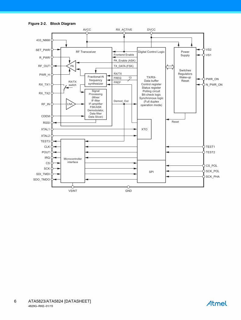
Figure 2-2. Block Diagram
SignalProcessing
(MixerIF-filter
IF-amplifierFSK/ASK
Demodulator,Data filter
Data Slicer)
TX/RX-Data buffer
Control registerStatus registerPolling circuitBit-check logic
Synchronous logic(Full duplex
operation mode)
Digital Control Logic PowerSupply
SwitchesRegulatorsWake-up
Reset
RF Transceiver
Fractional-Nfrequency
synthesizer
VS2
VS1
433_N868
PWR_H
CS
SDO_TMDO
IRQ
POUT
CLK
TEST3
XTAL2
XTAL1
RSSI
CDEM
RF_IN
RX_TX2
RX_TX1
RF_OUT
SET_PWR
R_PWR
DVCCRX_ACTIVEAVCC
GNDVSINT
LNA
SPI
XTO
Reset
PA
RX/TXswitch
Frontend Enable
PA_Enable (ASK)
Demod_Out
FREFFREQRX/TX
13
TX_DATA (FSK)
Microcontrollerinterface
SCK
SDI_TMDI
TEST2
TEST1
SCK_PHA
CS_POL
SCK_POL
N_PWR_ON
PWR_ON
ATA5823/ATA5824 [DATASHEET]4829G–RKE–01/15
6

3. Typical Key Fob Application for Bi-directional RKE
Figure 3-1. Typical Key Fob Application for Bi-directional RKE with 5dBm TX Power, 433.92MHz
Figure 3-1 shows a typical 433.92MHz RKE key fob application. The external components are 10 capacitors, 1 resistor, 2 inductors and a crystal. C1 to C3 are 68nF voltage supply blocking capacitors. C5 is a 10nF supply blocking capacitor. C6 is a 15nF fixed capacitor used for the internal quasi-peak detector and for the high-pass frequency of the data filter. C7 to C11 are RF matching capacitors in the range of 1pF to 33pF. L1 is a matching inductor of about 5.6nH to 56nH. L2 is a feed inductor of about 120nH. A load capacitor of 9pF for the crystal is integrated. R1 is typically 22k and sets the output power to about 5.5dBm. The loop antenna’s quality factor is somewhat reduced by this application due to the quality factor of L2 and the RX/TX switch. On the other hand, this lower quality factor is necessary to have a robust design with a bandwidth that is wide enough for production tolerances. Due to the single-ended and ground-referenced design, the loop antenna can be a free-form wire around the application as it is usually employed in RKE unidirectional systems. The Atmel® ATA5823/ATA5824 provides sufficient isolation and robust pulling behavior of internal circuits from the supply voltage as well as an integrated VCO inductor to allow this. Since the efficiency of a loop antenna is proportional to the square of the surrounded area, it is beneficial to have a large loop around the application board with a lower quality factor to relax the tolerance specification of the RF matching components and to get a high antenna efficiency in spite of their lower quality factor.
CS
NC
RSSICDEM
SCK
TEST3
SDI_TMDI
SDO_TMDOATA5823/ATA5824CLK
VCC VSSVSINT
XTAL2
+ Lithium cell
Loop antenna
AVCC
20 m
m x
0.4
mm
Microcontroller
13.25311 MHz
POUT
IRQ
NCNC
RF_IN
C7C11 C6
C3
C1
C2
433_N868
NC
NC
NC
RF_OUT
PWR_H
R_PWR
NC
AV
CC
VS
2
NC
NC
NC
VS
1
SE
TPW
R
TES
T1
DV
CC
CS
_PO
L
TES
T2
TXA
L1
NC
NC
NC
NC
RX
_AC
TIV
E
N_P
WR
_ON
SC
K_P
HA
SC
K_P
OL
PW
R_O
NR
X_T
X1
RX
_TX
2
NC
C9
C10
R1L2
L1
C8
C5
7ATA5823/ATA5824 [DATASHEET]4829G–RKE–01/15

4. Typical Car Application for Bi-directional RKE
Figure 4-1. Typical Car Application for Bi-directional RKE with 10dBm TX Power, 433.92MHz
Figure 4-1 shows a typical 433.92MHz VCC = 4.4V to 5.25V RKE car application. The external components are 11 capacitors, 1 resistor, 4 inductors, a SAW filter and a crystal. C1, C3 and C4 are 68nF voltage supply blocking capacitors. C2 is a 2.2µF supply blocking capacitor for the internal voltage regulator. C5 is a 10nF supply blocking capacitor. C6 is a 15nF fixed capacitor used for the internal quasi-peak detector and for the high-pass frequency of the data filter. C7 to C11 are RF matching capacitors in the range of 1pF to 33pF. L2 to L4 are matching inductors of about 5.6nH to 56nH. A load capacitor for the crystal of 9pF is integrated. R1 is typically 22kand sets the output power at RFOUT to about 10dBmSince a quarter wave or PCB antenna, which has high efficiency and wideband operation, is typically used here, it is recommended to use a SAW filter to achieve high sensitivity in case of powerful out-of-band blockers. L1, C10 and C9 together form a low-pass filter, which is needed to filter out the harmonics in the transmitted signal to meet regulations.
CS
NC
RSSICDEM
SCK
TEST3
SDI_TMDI
SDO_TMDO
CLK
VSINT
XTAL2
AVCC
50Ωconnector
SAW-Filter
20 m
m x
0.4
mm
13.25311 MHz
VCC = 4.4V to 5.25V
POUT
IRQ
NCNC
RF_IN
C7C11 C6
C3
C2C1 C4
433_N868
NC
NC
NCRF_OUT
PWR_H
R_PWR
NC
AV
CC
VS
2
NC
NC
NC
VS
1
SE
TPW
R
TES
T1
DV
CC
CS
_PO
L
TES
T2
TXA
L1
NC
NC
NC
NC
SC
K_P
H
SC
K_P
OL
RX
_AC
TIV
E
N_P
WR
_ON
PW
R_O
NR
X_T
X1
RX
_TX
2
NC
C10 C9RFOUT
R1L2
L1
L4
C8
C5
L3
VCC VSS
Microcontroller
ATA5823/ATA5824
ATA5823/ATA5824 [DATASHEET]4829G–RKE–01/15
8
5. RF Transceiver in Half-duplex Mode
According to Figure 2-2 on page 6, the RF transceiver consists of an LNA (Low-Noise Amplifier), PA (Power Amplifier), RX/TX switch, fractional-N frequency synthesizer and the signal processing part with mixer, IF filter, IF amplifier with analog RSSI, FSK/ASK demodulator, data filter and data slicer.
In receive mode the LNA pre-amplifies the received signal which is converted down to 226kHz intermediate frequency (IF), filtered and amplified before it is fed into an FSK/ASK demodulator, data filter and data slicer. The RSSI (Received Signal Strength Indicator) signal and the raw digital output signal of the demodulator are available at the pins RSSI and on TEST3 (open drain output). The demodulated data signal Demod_Out is fed into the digital control logic where it is evaluated and buffered as described in section “Digital Control Logic” on page 32.
In transmit mode the fractional-N frequency synthesizer generates the TX frequency which is fed into the PA. In ASK mode the PA is modulated by the signal PA_Enable. In FSK mode the PA is enabled and the signal TX_DATA (FSK) modulates the fractional-N frequency synthesizer. The frequency deviation is digitally controlled and internally fixed to about ±19.5kHz (see Table 6-1 on page 25 for exact values). The transmit data can also be buffered as described in section “Digital Control Logic” on page 32. A lock detector within the synthesizer ensures that the transmission will only start if the synthesizer is locked.
In half-duplex mode the RX/TX switch can be used to combine the LNA input and the PA output to a single antenna with a minimum of losses.
Transparent modes without buffering of RX and TX data are also available to allow protocols and coding schemes other than the internal supported Manchester encoding, like PWM and pulse position coding.
5.1 Low-IF Receiver
The receive path consists of a fully integrated low-IF receiver. It fulfills the sensitivity, blocking, selectivity, supply voltage and supply current specification needed to manufacture an automotive key fob for RKE and PEG systems without the use of a SAW blocking filter (see Figure 3-1 on page 7). The receiver can be connected to the roof antenna in the car when using an additional blocking SAW front-end filter as shown in Figure 4-1 on page 8.
At 433.92MHz the receiver has a typical system noise figure of 6.5dB, a system I1dBCP of –30dBm and a system IIP3 of –20dBm. The signal path is linear for disturbers up to the I1dBCP and there is hence no AGC or switching of the LNA needed to achieve a better blocking performance. This receiver uses an IF of about 226kHz (see Section 14. “Electrical Characteristics: General” on page 61 number 2.10 for exact values), the typical image rejection is 30dB and the typical 3dB system bandwidth is 220kHz (fIF = 226kHz ±110kHz, flo_IF = 116kHz and fhi_IF = 336kHz). The demodulator needs a signal to noise ratio of 8dB for 20Kbit/s Manchester with ±19.5kHz frequency deviation in FSK mode, thus, the resulting sensitivity at 433.92MHz is typically –105.5dBm.
Due to the low phase noise and spurious of the synthesizer in receive mode(1) together with the eighth order integrated IF filter the receiver has a better selectivity and blocking performance than more complex double superhet receivers, without using external components and without numerous spurious receiving frequencies.
Note: 1. –120dBC/Hz at ±1MHz and –72dBC at ±fXTO at 433.92MHz
A low-IF architecture is also less sensitive to second-order intermodulation (IIP2) than direct conversion receivers where every pulse or amplitude modulated signal (especially the signals from TDMA systems like GSM) demodulates to the receiving signal band at second-order non-linearities.
9ATA5823/ATA5824 [DATASHEET]4829G–RKE–01/15

5.2 Input Matching at RF_IN
The measured input impedances as well as the values of a parallel equivalent circuit of these impedances can be seen in Table 5-1. The highest sensitivity is achieved with power matching of these impedances to the source impedance of 50.
The matching of the LNA Input to 50 was done with the circuit according to Figure 5-1 and with the values of the matching elements given in Table 5-2. The reflection coefficients were always ≤ –10dB. Note that value changes of C1 and L1 may be necessary to compensate individual board layout parasitics. The measured typical FSK and ASK Manchester code sensitivities with a Bit Error Rate (BER) of 10-3 are shown in Table 5-3 on page 10 and Table 5-4 on page 10. These measurements were done with multilayer inductors having quality factors according to Table 5-2, resulting in estimated matching losses of 0.8dB at 315MHz and 0.8dB at 433.92MHz. These losses can be estimated when calculating the parallel equivalent resistance of the inductor with Rloss = 2 f L QL and the matching loss with 10 log(1+RIn_p/Rloss).
With an ideal inductor, for example, the sensitivity at 433.92MHz/FSK/20Kbit/s/ ±19.5kHz/Manchester can be improved from –105.5dBm to –106.7dBm. The sensitivity also depends on the values in the registers of the control logic which examines the incoming data stream. The examination limits must be programmed in control registers 5 and 6. The measurements in Table 5-3 and Table 5-4 on page 10 are based on the values of registers 5 and 6 according to Table 11-3 on page 55.
Figure 5-1. Input Matching to 50
Table 5-1. Measured Input Impedances of the RF_IN Pin
fRF/MHz ZIn(RF_IN) RIn_p//CIn_p
315 (44-j233) 1278//2.1pF
433.92 (32-j169) 925//2.1pF
Table 5-2. Input Matching to 50
fRF/MHz C1/pF L1/nH QL1
315 2.4 47 65
433.92 1.8 27 67
Table 5-3. Measured Typical Sensitivity 433.92MHz, FSK, ±19.5kHz, Manchester, BER = 10-3
RF FrequencyBR_Range_0
1.0Kbit/sBR_Range_0
2.4Kbit/sBR_Range_1
5.0Kbit/sBR_Range_2
10Kbit/sBR_Range_3
20Kbit/s
315MHz –109.5dBm –110.0dBm –109.0dBm –107.5dBm –106.5dBm
433.92MHz –108.5dBm –109.0dBm –108.0dBm –106.5dBm –105.5dBm
Table 5-4. Measured Typical Sensitivity 433.92 MHz, 100% ASK, Manchester, BER = 10-3
RF FrequencyBR_Range_0
1.0Kbit/sBR_Range_0
2.4Kbit/sBR_Range_1
5.0Kbit/sBR_Range_2
10Kbit/s
315MHz –117.0dBm –117.0dBm –114.5dBm –112.5dBm
433.92MHz –116.0dBm –116.0dBm –113.5dBm –111.5dBm
L1
C1 4RF_IN
ATA5823/ATA5824
ATA5823/ATA5824 [DATASHEET]4829G–RKE–01/15
10

5.3 Sensitivity versus Supply Voltage, Temperature and Frequency Offset
To calculate the behavior of a transmission system it is important to know the reduction of the sensitivity due to several influences. The most important are frequency offset due to crystal oscillator (XTO) and crystal frequency (XTAL) errors, temperature and supply voltage dependency of the noise figure and IF filter bandwidth of the receiver. Figure 5-2 shows the typical sensitivity at 433.92MHz/FSK/20Kbit/s/±19.5kHz/Manchester versus the frequency offset between transmitter and receiver at Tamb = –40°C, +25°C and +105°C and supply voltage VS = VS1 = VS2 = 2.15V, 3.0V and 3.6V.
Figure 5-2. Measured Sensitivity 433.92MHz/FSK/20Kbit/s/±19.5kHz/Manchester versus Frequency Offset, Temper-ature and Supply Voltage
As can be seen in Figure 5-2 on page 11 the supply voltage has almost no influence on the sensitivity. The temperature has an influence of about +1.5/–0.7dB and a frequency offset of ±85kHz also influences by about ±1dB. All these influences, combined with the sensitivity of a typical IC (–105.5dBm), are then within a range of –102.5dBm and –107dBm overtemperature, supply voltage and frequency offset. The integrated IF filter has an additional production tolerance of ±10kHz, hence, a frequency offset between the receiver and the transmitter of ±75kHz can be accepted for XTAL and XTO tolerances.
Note: For the demodulator used in the Atmel ATA5823/ATA5824, the tolerable frequency offset does not change with the data frequency, hence, the value of ±75kHz is valid for 1Kbit/s to 20Kbit/s.
This small sensitivity change over supply voltage, frequency offset and temperature is very unusual in such a receiver. It is achieved by an internal, very fast and automatic frequency correction in the FSK demodulator after the IF filter, which leads to a higher system margin. This frequency correction tracks the input frequency very quickly, if however, the input frequency makes a larger step (e.g., if the system changes between different communication partners), the receiver has to be restarted. This can be done by switching back to IDLE mode and then again to RX mode. For that purpose, an automatic mode is also available. This automatic mode switches to IDLE mode and back into RX mode every time a bit error occurs (see section “Digital Control Logic” on page 32).
5.4 Frequency Accuracy of the Crystals in Bi-directional RKE/PEG
The XTO is an amplitude regulated Pierce type oscillator with integrated load capacitors. The initial tolerances (due to the frequency tolerance of the XTAL, the integrated capacitors on XTAL1, XTAL2 and the XTO’s initial transconductance gm) can be compensated to a value within ±0.5ppm by measuring the CLK output frequency and tuning of fRF by programming the control registers 2 and 3 (see Table 9-7 on page 34 and Table 9-10 on page 35). The XTO then has a remaining influence of less than ±2ppm overtemperature and supply voltage due to the bandgap controlled gm of the XTO. Thus only 2.5ppm add to the frequency stability of the used crystals overtemperature and aging.
The needed frequency stability of the used crystals overtemperature and aging is hence ±75kHz/433.92MHz – 2 ±2.5ppm = ±167.84ppm for 433.92MHz. Thus, the used crystals in receiver and transmitter each need to be better than ±83.9ppm for 433.92MHz.
-109-108-107-106-105-104-103-102-101-100
-99-98-97-96-95
-110
Sens
itivi
ty (d
Bm
)
-60 40 60 10080-40-80-100 0Frequency Offset (kHz)
20-20
VS = 3.0V Tamb = -40°CVS = 3.6V Tamb = -40°C
VS = 3.0V Tamb = +25°CVS = 3.6V Tamb = +25°CVS = 2.15V Tamb = +105°CVS = 3.0V Tamb = +105°CVS = 3.6V Tamb = +105°C
VS = 2.15V Tamb = +25°C
VS = 2.15V Tamb = -40°C
11ATA5823/ATA5824 [DATASHEET]4829G–RKE–01/15

5.5 Frequency Accuracy of the Crystals in a Combined RKE/PEG and TPM System
In a tire pressure measurement system working at 433.92MHz and using a TPM transmitter Atmel® ATA5757 and a transceiver Atmel ATA5824 as a receiver, the higher frequency tolerances and the tolerance of the frequency deviation of this transmitter has to be considered.
In the TPM transmitter the crystal has an frequency error overtemperature –40°C to +125°C, aging and tolerance of ±80ppm (±34.7kHz at 433.92MHz). The tolerances of the XTO, the capacitors used for FSK-Modulation and the stray capacitors, causing an additional frequency error of ±30ppm (±13kHz at 433.92MHz). The frequency deviation of such a transmitter varies between ±16kHz and ±24kHz, since a higher frequency deviation is equivalent to an frequency error, this has to be considered as an additional ±24kHz – ±19.5kHz = ±4.5kHz frequency tolerance. All tolerances added, these transmitters have a worst case frequency offset of ±52.2kHz.
For the transceiver in the car a tolerance of ±75kHz – ±52.2kHz = ±22.8kHz (±52.5ppm) remains. The needed frequency stability of the used crystals overtemperature and aging is ±52.5ppm – ±2.5ppm = ±50ppm. The aging of such a crystal is ±10ppm leaving reasonable ±40ppm for the temperature dependency of the crystal frequency in the car.
Since the transceiver in the car is able to receive these TPM transmitter signals with high frequency offsets, the component specification in the key can be largely relaxed.
This system calculation is based on worst case tolerances of all the components, this leads in practice to a system with margin.
For a 315MHz TPM system using a TPM transmitter Atmel ATA5756 and a transceiver Atmel ATA5823 as receiver the same calculation must be done, but since the RF frequency is lower, every ppm of crystal tolerances results in less frequency offset and either the system can have higher tolerances or a higher margin there.
5.6 RX Supply Current versus Temperature and Supply Voltage
Table 5-5 shows the typical supply current at 433.92MHz of the transceiver in RX mode versus supply voltage and temperature with VS = VS1 = VS2. As can be seen the supply current at VS = 2.15V and Tamb = –40°C is less than at VS = 3V/Tamb = 25° which helps to enlarge the battery lifetime within a key fob application because this is also the operation point where a lithium cell has the worst performance. The typical supply current at 315MHz in RX mode is about the same as for 433.92MHz.
Table 5-5. Measured 433.92MHz Receive Supply Current in FSK mode
VS = VS1 = VS2 2.15V 3.0V 3.6V
Tamb = –40°C 8.2mA 8.8mA 9.2mA
Tamb = 25°C 9.7mA 10.3mA 10.8mA
Tamb = 105°C 11.2mA 11.9mA 12.4mA
ATA5823/ATA5824 [DATASHEET]4829G–RKE–01/15
12

5.7 Blocking, Selectivity
As can be seen in Figure 5-3, Figure 5-4 and Figure 5-5 on page 13, the receiver can receive signals 3dB higher than the sensitivity level in presence of large blockers of –44.5dBm/-36.0dBm with small frequency offsets of ±1±10MHz.
Figure 5-3 and Figure 5-4 on page 13 shows the close-in and narrow-band blocking and Figure 5-5 on page 13 the wide-band blocking characteristic. The measurements were done with a useful signal of 433.92MHz/FSK/20Kbit/s/±19.5kHz/Manchester with a level of –105.5dBm + 3dB = –102.5dBm which is 3dB above the sensitivity level. The figures show by how much a continuous wave signal can be larger than –102.5dBm until the BER is higher than 10-3. The measurements were done at the 50 input according to Figure 5-1 on page 10 At 1MHz, for example, the blocker can be 58dBC higher than –102.5dBm which is –102.5dBm +58dBC = –44.5dBm. These blocking figures, together with the good intermodulation performance, avoid the additional need of a SAW filter in the key fob application.
Figure 5-3. Close In 3dB Blocking Characteristic and Image Response at 433.92MHz
Figure 5-4. Narrow Band 3dB Blocking Characteristic at 433.92MHz
Figure 5-5. Wide Band 3dB Blocking Characteristic at 433.92MHz
-0.2 0 0.2 0.4-1.0 -0.8 -0.6 -0.4
Distance of Interfering to Receiving Signal (MHz)
0.6 0.8 1.0
70
50
60
40
20
30
Blo
ckin
g Le
vel (
dBC
)
10
-10
0
70
50
60
40
20
30
Blo
ckin
g (d
BC
)
10
-10
0
-1 0 1 2-5 -4 -3 -2
Distance of Interfering to Receiving Signal (MHz)3 4 5
-10 0 10 20-50 -40 -30 -20
Distance of Interfering to Receiving Signal (MHz)30 40 50
70
80
50
60
40
20
30
Blo
ckin
g (d
BC
)
10
-10
0
13ATA5823/ATA5824 [DATASHEET]4829G–RKE–01/15

Table 5-6 shows the blocking performance measured relative to –102.5dBm for some frequencies. Note that sometimes theblocking is measured relative to the sensitivity level –105.5dBm (denoted dBS) instead of the carrier –102.5dBm (denoteddBC).
The Atmel® ATA5823/ATA5824 can also receive FSK and ASK modulated signals if they are much higher than the I1dBCP. It can typically receive useful signals at +10dBm. This is often referred to as the nonlinear dynamic range which is the maximum to minimum receiving signal which is 115.5dB for 433.92MHz/FSK/20Kbit/s/±19.5kHz/ Manchester. This value is useful if two transceivers have to communicate and are very close to each other.
In a keyless entry system there is another blocking characteristic that has to be considered. A keyless entry system has a typical service range of about 30 m with a receiver sensitivity of about –106dBm to –109dBm. In some cases, large blockers limit this service range, and it is important to know how large this blockers can be until the system doesn’t work anymore and the user has to use its key. With a recommended sensitivity of about –85dBm, the system works just around the car. Figure 5-6 and Figure 5-7 on page 15 show the blocking performance in this important case with a useful signal of –85dBm 433.92MHz/FSK/20Kbit/s/±19.5kHz/ Manchester.
As can be seen the system works even with blockers above the compression point. This is due to a wide bandwidth automatic gain control that begins to work if blockers above the compression point are at the antenna input and increasing the current in the LNA/Mixer to get a better compression point needed to handle these large blockers.
Figure 5-6. ±2.5MHz Blocking Characteristic for –85dBm Useful Signal at 433.92MHz
Table 5-6. Blocking 3 dB Above Sensitivity Level with BER < 10-3
Frequency Offset Blocker Level Blocking
+0.75MHz –47.5dBm 55.0dBC/58.0dBS
–0.75MHz –47.5dBm 55.0dBC/58.0dBS
+1.0MHz –44.5dBm 58.0dBC/61.0dBS
–1.0MHz –44.5dBm 58.0dBC/61.0dBS
+1.5MHz –42.0dBm 60.5dBC/63.5dBS
–1.5MHz –42.0dBm 60.5dBC/63.5dBS
+10MHz –35.5dBm 67.0dBC/70.0dBS
–10MHz –35.5dBm 67.0dBC/70.0dBS
-0.5 0 0.5 1.0-2.5 -2.0 -1.5 -1.0
Distance of Interfering to Receiving Signal (MHz)1.5 2.0 2.5
-20
-40
-30
-50
-70
-60
Blo
cker
Lev
el (d
Bm
)
-80
-90
ATA5823/ATA5824 [DATASHEET]4829G–RKE–01/15
14

Figure 5-7. ±50MHz Blocking Characteristic for –85dBm Useful Signal at 433.92MHz
This high blocking performance makes it even possible for some applications using quarter wave whip antennas to use a simple LC band-pass filter instead of a SAW filter in the receiver. When designing such a LC filter, take into account that the 3dB blocking at 433.92MHz/2 = 216.96MHz is 42dBC and at 433.92MHz/3 = 144.64MHz is 47dBC a . And especially that at 3 (433.92MHz + 226kHz)+226kHz = 1302.664MHz the receiver has a second LO harmonic receiving frequency with only 17dBC blocking.
5.8 Inband Disturbers, Data Filter, Quasi-peak Detector, Data Slicer
If a disturbing signal falls into the received band, or a blocker is not a continuous wave, the performance of a receiver strongly depends on the circuits after the IF filter. Hence the demodulator, data filter and data slicer are important in that case.
The data filter of the Atmel® ATA5823/ATA5824 implies a quasi-peak detector. This results in a good suppression of above mentioned disturbers and exhibits a good carrier to noise performance. The required ratio of useful signal to disturbing signal, at a BER of 10-3 is less than 12dB in ASK mode and less than 3dB (BR_Range_0 ... BR_Range_2) and 6dB (BR_Range_3) in FSK mode. Due to the many different possible waveforms these numbers are measured for signal as well as for disturbers with peak amplitude values. Note that these values are worst case values and are valid for any type of modulation and modulating frequency of the disturbing signal as well as the receiving signal. For many combinations, lower carrier to disturbing signal ratios are needed.
5.9 TEST3 Output
The internal raw output signal of the demodulator Demod_Out is available at pin TEST3. TEST3 is an open drain output and must be connected to a pull-up resistor if it is used (typically 100k), otherwise no signal is present at that pin. This signal is mainly used for debugging purposes during the setup of a new application, since the received data signal can be seen there without any digital processing.
-10 0 10 20-50 -40 -30 -20
Distance of Interfering to Receiving Signal (MHz)30 40 50
-20
-10
0
-40
-30
-50
-70
-60
Blo
cker
Lev
el (d
Bm
)-80
-90
15ATA5823/ATA5824 [DATASHEET]4829G–RKE–01/15

5.10 RSSI Output
The output voltage of the pin RSSI is an analog voltage, proportional to the input power level. Using the RSSI output signal, the signal strength of different transmitters can be distinguished. The usable dynamic range of the RSSI amplifier is 70dB, the input power range PRFIN is –115dBm to –45dBm and the gain is 8mV/dB. Figure 5-8 on page 16 shows the RSSI characteristic of a typical device at 433.92MHz with VS1 = VS2 = 2.15V to 3.6V and Tamb = –40°C to +105°C with a matched input according to Table 5-2 on page 10 and Figure 5-1 on page 10. At 315MHz about 1dB less signal level is needed for the same RSSI results.
Figure 5-8. Typical RSSI Characteristic at 433.92MHz versus Temperature and Supply Voltage
5.11 Frequency Synthesizer and Channel Selection
The synthesizer is a fully integrated fractional-N design with internal loop filters for receive and transmit mode. The XTO frequency fXTO is the reference frequency FREF for the synthesizer. The bits FR0 to FR12 in control registers 2 and 3 (see Table 9-7 on page 34 and Table 9-10 on page 35) are used to adjust the deviation of fXTO. In half-duplex transmit mode, at 433.92MHz, the carrier has a phase noise of –111dBC/Hz at 1MHz and spurious at FREF of –70dBC with a high PLL loop bandwidth allowing the direct modulation of the carrier with 20Kbit/s Manchester data. Due to the closed loop modulation, any spurious caused by this modulation are effectively filtered out as can be seen in Figure 5-11 on page 18. In RX mode the synthesizer has a phase noise of –120dBC/Hz at 1MHz and spurious of –72dBC.
The initial tolerances of the crystal oscillator due to crystal frequency tolerances, internal capacitor tolerances and the parasitics of the board have to be compensated at manufacturing setup with control registers 2 and 3 as can be seen in Table 6-1 on page 25. The other control words for the synthesizer needed for ASK, FSK and receive/transmit switching are calculated internally. The RF (Radio Frequency) resolution is equal to the XTO frequency divided by 16384 which is 777.1Hz at 315.0MHz and 808.9Hz at 433.92MHz.
The frequency control word FREQ in control registers 2 and 3 can be programmed in the range of 1000 to 6900, hence every frequency within the 433MHz ISM bands can be programmed as receive and as transmit frequency and the position of channels within these ISM bands can be chosen arbitrarily (see Table 6-1 on page 25).
Care must be taken regarding the harmonics of the CLK output signal as well as to the harmonics produced by a microprocessor clocked with it, since these harmonics can disturb the reception of signals. In a single channel system using FREQ = 3803 to 4053 ensures that harmonics of this signal, do not disturb the receive mode.
400
500
600
700
800
900
1000
1100
-80 -70 -60 -50-120 -110 -100 -90PRF_IN (dBm)
V RSS
I (m
V)
-40
max.
min. typ.
ATA5823/ATA5824 [DATASHEET]4829G–RKE–01/15
16

5.12 FSK/ASK Transmission
Due to the fast modulation capability of the synthesizer and the high resolution, the carrier can be internally FSK modulated which simplifies the application of the transceiver. The deviation of the transmitted signal is ±24 digital frequency steps of the synthesizer which is equal to ±18.65kHz for 315MHz and ±19.41kHz for 433.92MHz.
Due to closed loop modulation with PLL filtering, the modulated spectrum is very clean, meeting ETSI and CEPT regulations when using a simple LC filter for the power amplifier harmonics as it is shown in Figure 4-1. In ASK mode the frequency is internally connected to the center of the FSK transmission and the power amplifier is switched on and off to perform the modulation. Figure 5-9 to Figure 5-11 on page 18 show the spectrum of the FSK modulation with pseudo-random data with 20Kbit/s/±19.41kHz/Manchester and 5dBm output power.
Figure 5-9. FSK-modulated TX Spectrum (433.92MHz/20Kbit/s/19.41kHz/Manchester Code)
Atten 20 dB
VAvg50
S3 FCW1 S2
Ref 10 dBm
Span 30 MHzSweep 7.5 ms (401 pts)
Center 433.92 MHzVBW 100 kHzRes BW 100 kHz
SampLog
dB/10
17ATA5823/ATA5824 [DATASHEET]4829G–RKE–01/15

Figure 5-10. Unmodulated TX Spectrum 433.92MHz - 19.41kHz (fFSK_L)
Figure 5-11. FSK-modulated TX Spectrum (433.92MHz/20Kbit/s/±19.41kHz/Manchester Code)
Atten 20 dB
VAvg50
S3 FCW1 S2
Ref 10 dBm
Span 1 MHzSweep 27.5 ms (401 pts)
Center 433.92 MHzVBW 10 kHzRes BW 10 kHz
SampLog
dB/10
Atten 20 dB
VAvg50
S3 FCW1 S2
Ref 10 dBm
Span 1 MHzSweep 27.5 ms (401 pts)
Center 433.92 MHzVBW 10 kHzRes BW 10 kHz
SampLog
dB/10
ATA5823/ATA5824 [DATASHEET]4829G–RKE–01/15
18

5.13 Output Power Setting and PA Matching at RF_OUT
The Power Amplifier (PA) is a single-ended open collector stage which delivers a current pulse which is nearly independent of supply voltage, temperature and tolerances due to band-gap stabilization. Resistor R1 (see Figure 5-12 on page 20) sets a reference current which controls the current in the PA. A higher resistor value results in a lower reference current, a lower output power and a lower current consumption of the PA. The usable range of R1 is 15k to 56k. The PWR_H pin switches the output power range between about 0dBm to 5dBm (PWR_H = GND) and 5dBm to 10dBm (PWR_H = AVCC) by multiplying this reference current with a factor 1 (PWR_H = GND) and 2.5 (PWR_H = AVCC) which corresponds to about 5dB more output power.
If the PA is switched off in TX mode, the current consumption without output stage and with VS1 = VS2 = 3V, Tamb = 25°C is typically 6.95mA for 315MHz and 433.92MHz.
The maximum output power is achieved with optimum load resistances RLopt according to Table 5-7 on page 20. The compensation of the 1.0pF output capacitance of the RF_OUT pin will be achieved by absorbing it into the matching network, consisting of L1, C1, C3 as shown in Figure 5-12 on page 20. There must be also a low resistive DC path to AVCC to deliver the DC current of the power amplifier's last stage. The matching of the PA output was done with the circuit according to Figure 5-12 on page 20 with the values in Table 5-7. Note that value changes of these elements may be necessary to compensate individual board layout parasitics.
Example: According to Table 5-7 on page 20, with a frequency of 433.92MHz and output power of 11dBm, the overall current consumption is typically 17.8mA. Hence the PA needs 17.8mA - 6.95mA = 10.85mA in this mode which corresponds to an overall power amplifier efficiency of the PA of (10(11dBm/10) 1mW)/(3V 10.85mA) 100% = 38.6% in this case.
Using a higher resistor in this example of R1 = 1.091 22k = 24k results in 9.1% less current in the PA of 10.85mA/1.091 = 9.95mA and 10 log(1.091) = 0.38dB less output power if using a new load resistance of 300 1.091 = 327. The resulting output power is then 11dBm – 0.38dB = 10.6dBm and the overall current consumption is 6.95mA + 9.95mA = 16.9mA.
The values of Table 5-7 on page 20 were measured with standard multi-layer chip inductors with quality factors Q according to Table 5-7 on page 20.
Looking to the 433.92MHz/11dBm case with the quality factor of QL1 = 43 the loss in this inductor L1 is estimated with the parallel equivalent resistance of the inductor Rloss = 2 f L1 QL1 and the matching loss with 10 log (1 + RLopt/Rloss) which is equal to 0.32dB losses in this inductor. Taking this into account the PA efficiency is then 42% instead of 38.6%.
Be aware that the high power mode (PWR_H = AVCC) can only be used with a supply voltage higher than 2.7V, whereas the low power mode (PWR_H = GND) can be used down to 2.15V as can be seen in the section “Electrical Characteristics: General” on page 61.
The supply blocking capacitor C2 (10nF) in Figure 5-12 on page 20 has to be placed close to the matching network because of the RF current flowing through it.
An internal programmable resistor SETPWR is programmable with the control register 8, described in Table 9-25 on page 39. It can be used in conjunction with an external resistor to adjust the output power by connection it. To do that the output power should be adjusted with an external resistor about 50% lower than needed for the target output power and reduced with the programmable resistor during production test until the target power is as close as possible to the target. For example, if using 433.92MHz at 5dBm, a resistor of 12k instead of 24k is used and values of PWSET between 25 and 29 can be used to achieve an output power within 5dBm ±0.5dB over production. Note that this resistor is temperature stable but has tolerances of ±20% and introduces, therefore, additional output power tolerances, it is recommended to adjust output power during the production test if using the SETPWR resistor.
19ATA5823/ATA5824 [DATASHEET]4829G–RKE–01/15

Figure 5-12. Power Setting and Output Matching
5.14 Output Power and TX Supply Current versus Supply Voltage and Temperature
Table 5-8 shows the measurement of the output power for a typical device with VS1 = VS2 = VS in the 433.92MHz and 6.2dBm case versus temperature and supply voltage measured according to Figure 5-12 on page 20 with components according to Table 5-7 on page 20. As opposed to the receiver sensitivity the supply voltage has here the major impact on output power variations because of the large signal behavior of a power amplifier. Thus a 5V system using the internal voltage regulator shows much less variation than a 2.15V to 3.6V battery system because the AVCC supply voltage is 3.25V ±0.25V for a 5V system.
The reason is that the amplitude at the output RF_OUT with optimum load resistance is AVCC – 0.4V and the power is proportional to (AVCC – 0.4V)2 if the load impedance is not changed. This means that the theoretical output power reduction if reducing the supply voltage from 3.0V to 2.15V is 10 log ((3V – 0.4V)2/(2.15V – 0.4V)2) = 3.4dB. Table 5-8 shows that principle behavior in the measurements. This is not the same case for higher voltages, since here, increasing the supply voltage from 3V to 3.6V should theoretical increase the power by 1.8dB, but only 0.9dB in the measurements shows that the amplitude does not increase with the supply voltage because the load impedance is optimized for 3V and the output amplitude stays more constant because of the current source nature of the output.
Table 5-7. Measured Output Power and Current Consumption with VS1 = VS2 = 3V, Tamb = 25°C
Frequency (MHz)
TX Current (mA)
Output Power (dBm)
R1 (k) VPWR_H RLopt ()
L1 (nH) QL1
C1 (pF)
C3 (pF)
315 8.5 0.4 56 0 2500 82 28 1.5 0
315 10.5 5.7 27 0 920 68 32 2.2 0
315 16.7 10.5 27 AVCC 350 56 35 3.9 0
433.92 8.6 0.1 56 0 2300 56 40 0.75 0
433.92 11.2 6.2 22 0 890 47 38 1.5 0
433.92 17.8 11 22 AVCC 300 33 43 2.7 0
RFOUT10
RF_OUT
VPWR_H
AVCC
ATA5823/ATA5824
9
PWR_H
8R_PWR
C2
C1
L1
C3
R1
ATA5823/ATA5824 [DATASHEET]4829G–RKE–01/15
20

.
Table 5-9 shows the relative changes of the output power of a typical device compared to 3.0V/25°C. As can be seen, a temperature change to –40°C as well as to +105°C reduces the power by less than 1dB due to the band-gap regulated output current. Measurements of all the cases in Table 5-7 on page 20 overtemperature and supply voltage have shown about the same relative behavior as shown in Table 5-9.
5.15 RX/TX Switch
The RX/TX switch decouples the LNA from the PA in TX mode, and directs the received power to the LNA in RX mode. To do this, it has a low impedance to GND in TX mode and a high impedance to GND in RX mode. The pin 38 (RX_TX2) must always be connected to GND in the application. To design a proper RX/TX decoupling a linear simulation tool for radio frequency design together with the measured device impedances of Table 5-1 on page 10, Table 5-7 on page 20, Table 5-10 on page 21 and Table 5-11 on page 22 should be used. The exact element values have to be found on board. Figure 5-13 on page 21 shows an approximate equivalent circuit of the switch. The principal switching operation is described here according to the application of Figure 3-1 on page 7. The application of Figure 4-1 on page 8 works similarly.
.
Figure 5-13. Equivalent Circuit of the Switch
Table 5-8. Measured Output Power and Supply Current at 433.92MHz, PWR_H = GND
VS = VS1 = VS2 2.15V 3.0V 3.6V
Tamb = –40°C9.25mA3.2dBm
10.19mA5.5dBm
10.78mA6.2dBm
Tamb = +25°C10.2mA3.4dBm
11.19mA6.2dBm
11.79mA7.1dBm
Tamb = +105°C10.9mA3.0dBm
12.02mA5.4dBm
12.73mA6.3dBm
Table 5-9. Measurements of Typical Output Power Relative to 3V/25°C
VS = VS1 = VS2 2.15V 3.0V 3.6V
Tamb = –40°C –3.0dB –0.7dB 0dB
Tamb = +25°C –2.8dB 0dB +0.9dB
Tamb = +105°C –3.2dB –0.8dB +0.1dB
Table 5-10. Impedance of the RX/TX Switch RX_TX2 Shorted to GND
Frequency Z(RX_TX1) TX mode Z(RX_TX1) RX mode
315MHz (4.8 + j3.2) (11.3 – j214)
433.92MHz (4.5 + j4.3) (10.3 – j153)
1.6 nH
2.5 pF
RX_TX1
TX
11Ω 5Ω
21ATA5823/ATA5824 [DATASHEET]4829G–RKE–01/15

5.16 Matching Network in TX Mode
In TX mode the 20mm long and 0.4mm wide transmission line which is much shorter than /4 is approximately switched in parallel to the capacitor C9 to GND. The antenna connection between C8 and C9 has an impedance of about 50 looking from the transmission line into the loop antenna with pin RF_OUT, L2, C10, C8 and C9 connected (using a C9 without the added 7.6pF capacitor as discussed later). The transmission line can be approximated with a 16nH inductor in series with a 1.5 resistor, the closed switch can be approximated according to Table 5-10 with the series connection of 1.6nH and 5 in this mode. To have a parallel resonant high impedance circuit with little RF power going into it looking, from the loop antenna into the transmission line a capacitor of about 7.6pF to GND is needed at the beginning of the transmission line (this capacitor is later absorbed into C9, which is then higher as needed for 50 transformation). To keep the 50 impedance in RX mode at the end of this transmission line C7 has to be also about 7.6pF. This reduces the TX power by about 0.5dB at 433.92MHz compared to the case where the LNA path is completely disconnected.
5.17 Matching Network in RX Mode
In RX mode the RF_OUT pin has a high impedance of about 7k in parallel with 1.0pF at 433.92MHz as can be seen in Table 5-11 on page 22. This together with the losses of the inductor L2 with 120nH and QL2 = 25 gives about 3.7k loss impedance at RF_OUT. Since the optimum load impedance in TX mode for the power amplifier at RF_OUT is 890 the loss associated with the inductor L2 and the RF_OUT pin can be estimated to be 10 log(1 + 890/3700) = 0.95dB compared to the optimum matched loop antenna without L2 and RF_OUT. The switch represents, in this mode at 433.92MHz, about an inductor of 1.6nH in series with the parallel connection of 2.5pF and 2.0k. Since the impedance level at pin RX_TX1 in RX mode is about 50 there is only a negligible damping of the received signal by about 0.1dB. When matching the LNA to the loop antenna the transmission line and the 7.6pF part of C9 has to be taken into account when choosing the values of C11 and L1 so that the impedance seen from the loop antenna into the transmission line with the 7.6pF capacitor connected is 50.
Since the loop antenna in RX mode is loaded by the LNA input impedance the loaded Q of the loop antenna is lowered by about a factor of 2 in RX mode hence the antenna bandwidth is higher than in TX mode.
.
Note that if matching to 50, like in Figure 4-1 on page 8, a high Q wire wound inductor with a Q > 70 should be used for L2 to minimize its contribution to RX losses which will otherwise be dominant. The RX and TX losses will be in the range of 1.0dB there.
Table 5-11. Impedance RF_OUT Pin in RX mode
Frequency Z(RF_OUT)RX RP//CP
315MHz 36j502 7k1.0pF
433.92MHz 19j366 7k1.0pF
ATA5823/ATA5824 [DATASHEET]4829G–RKE–01/15
22

6. XTO
The XTO is an amplitude regulated Pierce oscillator type with integrated load capacitances (2 18pF with a tolerance of ±17%) hence CLmin = 7.4pF and CLmax = 10.6pF. The XTO oscillation frequency fXTO is the reference frequency FREF for the fractional-N synthesizer. When designing the system in terms of receiving and transmitting frequency offset the accuracy of the crystal and XTO have to be considered.
The synthesizer can adjust the local oscillator frequency for the initial frequency error in fXTO. This is done at nominal supply voltage and temperature with the control registers 2 and 3 (see Table 9-7 on page 34 and Table 9-10 on page 35). The remaining local oscillator tolerance at nominal supply voltage and temperature is then < ±0.5ppm. The XTO’s gm has very low influence of less than ±2ppm on the frequency at nominal supply voltage and temperature.
In a single channel system less than ±150ppm should be corrected to avoid that harmonics of the CLK output disturb the receive mode. If the CLK is not used, or carefully layouted on the application PCB (as needed for multi channel systems), more than ±150ppm can be compensated.
The additional XTO pulling is only ±2ppm, overtemperature and supply voltage. The XTAL versus temperature and its aging is then the main source of frequency error in the local oscillator.
The XTO frequency depends on XTAL properties and the load capacitances CL1, 2 at pin XTAL1 and XTAL2. The pulling of fXTO from the nominal fXTAL is calculated using the following formula:
ppm.
Cm is the crystal's motional, C0 the shunt and CLN the nominal load capacitance of the XTAL found in its datasheet. CL is the total actual load capacitance of the crystal in the circuit and consists of CL1 and CL2 in series connection.
Figure 6-1. XTAL with Load Capacitances
With Cm ≤ 14fF, C0 ≥ 1.5pF, CLN = 9pF and CL = 7.4pF to 10.6pF the pulling amounts to P ≤ ±100ppm and with Cm ≤ 7fF, C0 ≥ 1.5pF, CLN = 9pF and CL = 7.4pF to 10.6pF the pulling is P ≤ ±50ppm.
Since typical crystals have less than ±50ppm tolerance at 25°C, the compensation is not critical and can, in both cases, be done with the ±150ppm.
C0 of the XTAL has to be lower than CLmin/2 = 3.7pF for a Pierce oscillator type in order to not enter the steep region of pulling versus load capacitance where there is a risk of an unstable oscillation.
To ensure proper start-up behavior the small signal gain, and thus the negative resistance provided by this XTO at start is very large. For example oscillation starts up, even in worst case, with a crystal series resistance of 1.5k at C0 ≤ 2.2pF with this XTO. The negative resistance is approximately given by
with Z1, Z2 as complex impedances at pin XTAL1 and XTAL2 henceZ1 = –j/(2 fXTO CL1) + 5 andZ2 = –j/(2 fXTO CL2) + 5.
Z3 consists of crystals C0 in parallel with an internal 110k resistor henceZ3 = –j/(2 fXTO C0) /110k, gm is the internal transconductance between XTAL1 and XTAL2 with typically 19ms at 25°C.
PCm
2-------
CLN CL–
C0 CLN+ C0 CL+ ----------------------------------------------------------- 10
6=
C0
CL2CL1Cm
Lm Rm
CL = CL1 x CL2/ (CL1 + CL2)
XTAL
Crystal equivalent circuit
Re ZXTOcore ReZ1 Z3 Z2 Z3 Z1+ Z2 Z3 gm+
Z1 Z2 Z3 Z1 Z2 gm+ + +----------------------------------------------------------------------------------------------
=
23ATA5823/ATA5824 [DATASHEET]4829G–RKE–01/15

With fXTO = 13.5MHz, gm = 19ms, CL = 9pF, C0 = 2.2pF this results in a negative resistance of about 2k. The worst case fortechnological, supply voltage and temperature variations is then for C0 ≤ 2.2pF always higher than 1.5k
Due to the large gain at start, the XTO is able to meet a very low start-up time. The oscillation start-up time can be estimated with the time constant
After 10 to 20, an amplitude detector detects the oscillation amplitude and sets XTO_OK to High if the amplitude is large enough. This activates the CLK output if CLK_ON and CLK_EN in control register 3 are High (see Table 9-12 on page 35). Note that the necessary conditions of the DVCC voltage also have to be fulfilled (see Figure 6-2 on page 24 and Figure 7-1 on page 27).
To save current in IDLE and Sleep mode, the load capacitors partially are switched off in this modes with S1 and S2 seen in Figure 6-2 on page 24.
It is recommended to use a crystal with Cm = 3.0fF to 7.0fF, CLN = 9pF, Rm < 120 and C0 = 1.0pF to 2.2pF.
Lower values of Cm can be used, this increases slightly the start-up time. Lower values of C0 or higher values of Cm (up to 15fF) can also be used, this has only little influence to pulling.
Figure 6-2. XTO Block Diagram
To find the right values used in the control registers 2 and 3 (see Table 9-7 on page 34 and Table 9-10 on page 35) the relationship between fXTO and the fRF is shown in Table 6-1. To determine the right content, the frequency at pin CLK, as well as the output frequency at RF_OUT in ASK mode can be measured, than the FREQ value can be calculated according to Table 6-1 so that fRF is exactly the desired radio frequency.
2
4 2 fm2 Cm Re ZXTOcore Rm+
----------------------------------------------------------------------------------------------------=
8 pF 8 pF
XTAL1
Divider/16
CLK_EN(controlregister 3)
CLK_ON(controlregister 3)
DVCC_OK(from power supply)
Baud1
In IDLE mode and during Sleep mode (RX_Polling)the switches S1 and S2 are open.
XLimBaud0
&
Divider/3
XTO_OK(to reset logic)
Divider/1/2/4/8
/16
10 pF10 pF
Amplitudedetector
S2S1
fXDCLK
XTAL2 CLK
CL2CL1
fXTO
fDCLK
ATA5823/ATA5824 [DATASHEET]4829G–RKE–01/15
24

The variable FREQ depends on the bit PLL_MODE in control register 1 and the parameter FREQ2 and FREQ3, which are defined by the bits FR0 to FR12 in control register 2 and 3 and is calculated as follows:
FREQ = FREQ2 + FREQ3
Care must be taken with the harmonics of the CLK output signal fCLK, as well as to the harmonics produced by an microprocessor clocked with it, since these harmonics can disturb the reception of signals if they get to the RF input. In a single channel system the use of FREQ = 3803 to 4053 ensures that harmonics of this signal do not disturb the receive mode. In a multichannel system the CLK signal can either be not used or carefully layouted on the application PCB. The supply voltage of the microcontroller must also be carefully blocked in a multichannel system.
6.1 Pin CLK
Pin CLK is an output to clock a connected microcontroller. The clock frequency fCLK is calculated as follows:
The signal at CLK output has a nominal 50% duty cycle.
If the bit CLK_EN in control register 3 is set to 0, the clock is disabled permanently.
If the bit CLK_EN is set to 1 and bit CLK_ON (control register 3) is set to 0, the clock is disabled as well. If bit CLK_ON is set to 1 and thus the clock is enabled if the Bit-check is ok (RX, RX Polling, FD mode (Slave)), an event on pin N_PWR_ON occurs or the bit Power_On in the status register is 1.
Figure 6-3. Clock Timing
Table 6-1. Calculation of fRF
Frequency (MHz)
Pin 6433_N868
CREG1 Bit(4)
FS fXTO (MHz) fRF = fTX_ASK = fRX
fTX_FSK_L = fTX_FSK_L(FD) fTX_FSK_H fTX_FSK_H(FD)
Frequency Resolution
315.0 AVCC 1 12.73193fRF –
18.65kHzfRF +
18.65 kHzfRF +
208.23kHz777.1Hz
433.92 AVCC 0 13.25311fRF –
19.41kHzfRF +
19.41kHzfRF +
203.74kHz808.9Hz
fXTO 24 5FREQ 24,5+
16384--------------------------------+
fXTO 32 5FREQ 24,5+
16384--------------------------------+
fCLK
fXTO
3-----------=
CLK_ON(Control Register 3)
CLK_EN(Control Register 3)
CLK
DVCC VDVCC = 1.6V (typ)
25ATA5823/ATA5824 [DATASHEET]4829G–RKE–01/15

6.2 Basic Clock Cycle of the Digital Circuitry
The complete timing of the digital circuitry is derived from one clock. According to Figure 6-2 on page 24, this clock cycle TDCLK is derived from the crystal oscillator (XTO) in combination with a divider.
TDCLK controls the following application relevant parameters:
● Timing of the polling circuit including bit-check
● TX bit rate
The clock cycle of the Bit-check and the TX bit rate depends on the selected bit-rate range (BR_Range) which is defined in control register 6 (see Table 9-19 on page 37) and XLim which is defined in control register 4 (see Table 9-16 on page 36). This clock cycle TXDCLK is defined by the following formulas for further reference:
BR_Range BR_Range 0: TXDCLK = 8 TDCLK XLim
BR_Range 1: TXDCLK = 4 TDCLK XLim
BR_Range 2: TXDCLK = 2 TDCLK XLim
BR_Range 3: TXDCLK = 1 TDCLK XLim
fDCLK
fXTO
16-----------=
ATA5823/ATA5824 [DATASHEET]4829G–RKE–01/15
26

7. Power Supply
Figure 7-1. Power Supply
The supply voltage range of the Atmel® ATA5823/ATA5824 is 2.15V to 3.6V or 4.4V to 5.25V.
Pin VS1 is the supply voltage input for the range 2.15V to 3.6V and is used in battery applications using a single lithium 3V cell. Pin VS2 is the voltage input for the range 4.4V to 5.25V (car applications), in this case the voltage regulator V_REG regulates VS1 to typically 3.25V. If the voltage regulator is active, a blocking capacitor of 2.2µF has to be connected to VS1.
Pin VSINT is the voltage input for the Microcontroller_Interface and must be connected to the power supply of the microcontroller. The voltage range of VVSINT is 2.25V to 5.25V (see Figure 7-5 and Figure 7-6 on page 30).
AVCC is the internal operation voltage of the RF transceiver and is feed via the switch SW_AVCC by VS1. AVCC must be blocked on pin AVCC with a 68nF capacitor (see Figure 3-1 on page 7 and Figure 4-1 on page 8).
DVCC is the internal operation voltage of the digital control logic and is fed via the switch SW_DVCC by VS1. DVCC must be blocked on pin DVCC with 68nF (see Figure 3-1 on page 7 and Figure 4-1 on page 8).
Pin PWR_ON is an input to switch on the transceiver (active high).
Pin N_PWR_ON is an input for a push button and can also be used to switch on the transceiver (active low).
For current consumption reasons it is recommended to set N_PWR_ON to GND only temporarily. Otherwise an additional current flows because of a 50k pull-up resistor.
A voltage monitor generates the signal DVCC_OK if DVCC ≥ 1.6V typically.
V_Monitor(1.6V typ.)
V_REG13.25V typ.
SW_DVCC
DVCC_OK(to XTO andreset logic)
SW_AVCCOUT
R
S
FF1
Q
VSINT
DVCC_OKXTO_OK
OFFCMD(Command via SPI)
R0101
Qno change011
S0011
AVCC
DVCC
VS2
N_PWR_ONPWR_ON
VS1
IN
EN
≥ 1
&
≥ 1
27ATA5823/ATA5824 [DATASHEET]4829G–RKE–01/15

Figure 7-2. Flow Chart Operation Modes
7.1 OFF Mode
After connecting the power supply (battery) to pin VS1 and/or VS2 and VSINT, the transceiver is in OFF mode. In OFF mode AVCC and DVCC are disabled, resulting in very low power consumption (IS_OFF is typically ≤ 10nA in the key fob application Figure 3-1 on page 7 and ≤ 0.5µA in the car application Figure 4-1 on page 8). In OFF mode the transceiver is not programmable via the 4-wire serial interface.
7.2 IDLE Mode
In IDLE mode AVCC and DVCC are connected to the battery voltage (VS1).
From OFF mode the transceiver changes to IDLE mode if pin PWR_ON is set to 1 or pin N_PWR_ON is set to 0. This state transition is indicated by an interrupt at pin IRQ and the status bits Power_On = 1 or N_Power_On = 1.
In IDLE mode the RF transceiver is disabled and the power consumption IIDLE_VS1,2 is about 270 µA (CLK output OFF VS1 = VS2 = 3V). The exact value of this current is strongly dependent on the application and the exact operation mode, therefore check the section “Electrical Characteristics” for the appropriate application case.
Via the 4-wire serial interface a connected microcontroller can program the required parameter and enable the TX, RX polling, RX or FD mode.The transceiver can be set back to OFF mode by an OFF command via the 4-wire serial interface (the input level of pin PWR_ON must be 0 and pin N_PWR_ON = 1 before writing the OFF command)
OFF ModeAVCC = OFFDVCC = OFF
IDLE ModeAVCC = VS1DVCC = VS1
RX ModeRX PollingMode
FD Mode(Slave)
FD Mode(Master)TX Mode
AVCC = VS1; DVCC = VS1
OFF command andPin PWR_ON = 0 andPin N_ PWR_ON = 1
Pin PWR_ON = 1 orPin N_ PWR_ON = 0
OPM2
OP
M2
= 0
and
OP
M1
= 0
and
OP
M0
= 0
OPM1 OPM00 0 10 1 00 1 11 0 11 1 1
TX modeRX polling modeRX modeFD mode (maaster)FD mode (slave)
Table 7-1. Control Register 1
OPM2 OPM1 OPM0 Function
0 0 0 IDLE mode
ATA5823/ATA5824 [DATASHEET]4829G–RKE–01/15
28

7.3 Reset Timing and Reset Logic
If the transceiver is switched on (OFF mode to IDLE mode) DVCC and AVCC are ramping up as illustrated in Figure 7-3. The internal signal DVCC_RESET resets the digital control logic and sets the control register to default values. Bit DVCC_RST in the status register is set to 1.
After VDVCC exceeds 1.6V (typically) and the start-up time of the XTO is elapsed, the output clock at pin CLK is available.
DVCC_RST in the status register is set to 0 if VDVCC exceeds 1.6V, the start-up time of the XTO is elapsed and the status register is read via the 4-wire serial interface.
If VDVCC drops below 1.6V (typically) and pin N_PWR_ON = 1 and pin PWR_ON = 0 the transceiver switches to OFF mode.
Figure 7-3. Reset Timing
Figure 7-4. Reset Logic
DVCC, AVCC
DVCC_RESET
CLK
read status register
1.6V (typ)
OFF mode OFF modeIDLE mode IDLE, TX, RX, RX Polling, FD mode
VDVCC > 1.6V and the XTO is running
DVCC_RST(Status Register)
DVCC_OK
DVCC_RESET
XTO_OK
&
29ATA5823/ATA5824 [DATASHEET]4829G–RKE–01/15

7.4 Battery Application
The supply voltage range is 2.15V to 3.6V.
Figure 7-5. Battery Application
7.5 Car Application
The supply voltage range is 4.4V to 5.25V.
Figure 7-6. Car Application
VS
IN
OUT
IN
OUT
OUT
IN
VSINT
CLK
IRQ
CS
SCK
SDI_TMDI
SDO_TMDO
DVCC
RF transceiver
Digital control logic
ATA5823/ATA5824 Microcontroller
Mic
roco
ntro
ller_
Inte
rface
AVCC
VS2
2.15V to 3.6V
VS1
VS
IN
OUT
IN
OUT
OUT
IN
VSINT
CLK
IRQ
CS
SCK
SDI_TMDI
SDO_TMDO
DVCC
RF transceiver
Digital control logic
ATA5823/ATA5824 Microcontroller
Mic
roco
ntro
ller_
Inte
rface
AVCC
VS2
4.4V to 5.25V
VS1
ATA5823/ATA5824 [DATASHEET]4829G–RKE–01/15
30

8. Microcontroller Interface
The microcontroller interface is a level converter which converts all internal digital signals which are referred to the DVCC voltage, into the voltage used by the microcontroller. Therefore, the pin VSINT can be connected to the supply voltage of the microcontroller in the case the microcontroller has another supply voltage than the Atmel® ATA5823/ATA5824.
31ATA5823/ATA5824 [DATASHEET]4829G–RKE–01/15

9. Digital Control Logic
9.1 Register Structure
The configuration of the transceiver is stored in RAM cells. The RAM contains a 16 8-bit TX/RX data buffer and a 8 8-bit Control register and is write and readable via a 4-wire serial interface (CS, SCK, SDI_TMDI, SDO_TMDO).
The 1 8-bit status register is not part of the RAM and is readable via the 4-wire serial interface.
The RAM and the status information is stored as long as the transceiver is in any active mode (DVCC = VS1) and gets lost if the transceiver is in the OFF mode (DVCC = OFF).
After the transceiver is turned on via pin PWR_ON = High or pin N_PWR_ON = Low the control registers are in the default state.
Figure 9-1. Register Structure
IR1 FSIR0 OPM1OPM2 OPM0 Control Register 1 (ADR 0)
Control Register 2 (ADR 1)
Control Register 3 (ADR 2)
Control Register 4 (ADR 3)
Control Register 5 (ADR 4)
Control Register 6 (ADR 5)
Control Register 7 (ADR 6)
PLL_MODE
T_MODE
TX/RX Data Buffer:16 × 8 Bit
LSBMSB
FR3 FR2 FR0FR1FR6 FR5 FR4 P_MODE
FR9 FR8
XLimXSleep
FR7FR12 FR11 FR10 CLK_EN
CLK_ON
N_Power_On
DVCC_RST
Power_ON
Sleep3
Sleep1
Sleep0
Sleep2
Sleep4
ASK_NFSK
Lim_min5
Lim_min3
Lim_min0
Lim_min1
Lim_min2
Lim_min4
BitChk0
BitChk1
Lim_max5
Lim_max3
Lim_max0
Lim_max1
Lim_max2
Lim_max4
Baud0
Baud1
TX5 TX4 TX3 TX2 TX1 TX0POUT_DATA
POUT_SELECT
Status Register (ADR 16)
- = Don’t care
Control Register 8 (ADR 7)-
- - - - -
FE_MODE
PWSELECT
PWSET4
PWSET3
PWSET2
PWSET1
PWSET0
ATA5823/ATA5824 [DATASHEET]4829G–RKE–01/15
32

9.2 TX/RX Data Buffer
The TX/RX data buffer is used to handle the data transfer during RX and TX operations.
9.3 Control Register
To use the transceiver in different applications the transceiver can be configured by a microcontroller connected via the 4-wire serial interface.
9.3.1 Control Register 1 (ADR 0)
Table 9-1. Control Register 1 (Function of Bit 7 and Bit 6 in RX Mode)
IR1 IR0 Function (RX Mode)
0 0 Pin IRQ is set to 1 if 1 received byte is in the TX/RX data buffer or a receiving error occurred
0 1 Pin IRQ is set to 1 if 2 received bytes are in the TX/RX data buffer or a receiving error occurred
1 0 Pin IRQ is set to 1 if 4 received bytes are in the TX/RX data buffer or a receiving error occurred (default)
1 1 Pin IRQ is set to 1 if 12 received bytes are in the TX/RX data buffer or a receiving error occurred
Table 9-2. Control Register 1 (Function of Bit 7 and Bit 6 in TX Mode)
IR1 IR0 Function (TX Mode)
0 0 Pin IRQ is set to 1 if 1 byte still is in the TX/RX data buffer or the TX data buffer is empty
0 1 Pin IRQ is set to 1 if 2 bytes still are in the TX/RX data buffer or the TX data buffer is empty
1 0 Pin IRQ is set to 1 if 4 bytes still are in the TX/RX data buffer or the TX data buffer is empty (default)
1 1 Pin IRQ is set to 1 if 12 bytes still are in the TX/RX data buffer or the TX data buffer is empty
Note: The Bits IR0 and IR1 have no function in FD mode
Table 9-3. Control Register 1 (Function of Bit 5)
PLL_MODE Function
0 Adjustable range of FREQ: 3072 to 4095 (default), see Table 9-10 on page 35
1 Adjustable range of FREQ: 0 to 8191, see Table 9-11 on page 35
Table 9-4. Control Register 1 (Function of Bit 4)
FS Function (RX Mode, TX Mode, FD Mode)
0 Selected frequency 433MHz (default)
1 Selected frequency 315MHz
33ATA5823/ATA5824 [DATASHEET]4829G–RKE–01/15

9.3.2 Control Register 2 (ADR 1)
Table 9-5. Control Register 1 (Function of Bit 3, Bit 2 and Bit 1)
OPM2 OPM1 OPM0 Function
0 0 0 IDLE mode (default)
0 0 1 TX mode
0 1 0 RX polling mode
0 1 1 RX mode
1 0 0 -
1 0 1 -
1 1 0 -
1 1 1 -
Table 9-6. Control Register 1 (Function of Bit 0)
T_MODE Function
0 TX and RX function via TX/RX data buffer (default)
1Transparent mode, TX/RX data buffer disabled, TX modulation data stream via pin SDI_TMDI, RX modulation data stream via pin SDO_TMDO
Table 9-7. Control Register 2 (Function of Bit 7, Bit 6, Bit 5, Bit 4, Bit 3, Bit 2 and Bit 1)
FR626
FR525
FR424
FR323
FR222
FR121
FR020 Function
0 0 0 0 0 0 0 FREQ2 = 0
0 0 0 0 0 0 1 FREQ2 = 1
. . . . . . .
1 0 1 0 1 0 0 FREQ2 = 84 (default)
. . . . . . .
1 1 1 1 1 1 1 FREQ2 = 127
Note: Tuning of fRF LSB’s (total 13 bits), frequency trimming, resolution of fRF is fXTO/16384 which is approximately 800Hz (see section “XTO”, Table 6-1 on page 25)
Table 9-8. Control Register 2 (Function of Bit 0 in RX mode)
P_MODE Function (RX mode)
0 Pin IRQ is set to 1 if the Bit-check is successful (default)
1 No effect on pin IRQ if the Bit-check is successful
Table 9-9. Control Register 2 (Function of Bit 0 in TX mode)
P_MODE Function (TX mode)
0 Manchester modulator on (default)
1 Manchester modulator off (NRZ mode)
Note: Bit P_MODE has no function in FD mode
ATA5823/ATA5824 [DATASHEET]4829G–RKE–01/15
34

9.3.3 Control Register 3 (ADR 2)
Table 9-10. Control Register 3 (Function of Bit 7, Bit 6, Bit 5, Bit 4, Bit 3 and Bit 2 if Bit PLL_MODE = 0 (in Control Register 1)
FR12212
FR11211
FR10210
FR929
FR828
FR727 Function
X X X 0 0 0 FREQ3 = 3072
X X X 0 0 1 FREQ3 = 3200
X X X 0 1 0 FREQ3 = 3328
X X X 0 1 1 FREQ3 = 3456
X X X 1 0 0 FREQ3 = 3584
X X X 1 0 1 FREQ3 = 3712
X X X 1 1 0 FREQ3 = 3840(default)
X X X 1 1 1 FREQ3 = 3968
Note: Tuning of fRF MSB’s
Table 9-11. Control Register 3 (Function of Bit 7, Bit 6, Bit 5, Bit 4, Bit 3 and Bit 2 if Bit PLL_MODE = 1 (in Control Register 1)
FR12212
FR11211
FR10210
FR929
FR828
FR727 Function
0 0 0 0 0 0 FREQ3 = 0
0 0 0 0 0 1 FREQ3 = 128
0 0 0 0 1 0 FREQ3 = 256
. . . . . . .
0 1 1 1 1 0 FREQ3 = 3840 (default)
. . . . . . .
1 1 1 1 1 0 FREQ3 = 7936
1 1 1 1 1 1 FREQ3 = 8064
Note: Tuning of fRF MSB’s
Table 9-12. Control Register 3 (Function of Bit 1 and Bit 0)
CLK_EN CLK_ON Function (RX Mode, TX Mode, FD Mode)
0 X Clock output off (pin CLK)
1 0
Clock output off (pin CLK). Clock switched on by an event:
● Bit-check ok or
● event on pin N_PWR_ON or
● bit Power_On in the status register is 1
1 1 Clock output on (default)
Note: Bit CLK_ON is set to 1 if the Bit-check is ok (RX_Polling, RX mode), an event at pin N_PWR_ON occurs or the bit Power_On in the status register is 1.
35ATA5823/ATA5824 [DATASHEET]4829G–RKE–01/15

9.3.4 Control Register 4 (ADR 3)
Table 9-13. Control Register 4 (Function of Bit 7)
ASK_NFSK Function (TX Mode, RX Mode)
0 FSK mode (default)
1 ASK mode
Note: Bit ASK_NFSK has no function in FD mode
Table 9-14. Control Register 4 (Function of Bit 6, Bit 5, Bit 4, Bit 3 and Bit 2)
Sleep424
Sleep323
Sleep222
Sleep121
Sleep020
Function (RX Mode)
Sleep(TSleep = Sleep 1024 TDCLK XSleep)
0 0 0 0 0 0
0 0 0 0 1 1
. . . . .
1 1 0 0 024
(TSleep = 24 1024 TDCLK XSleep)(default)
. . . . .
1 1 1 1 1 31
Note: Bits Sleep0 ... Sleep4 have no function in TX mode and FD mode
Table 9-15. Control Register 4 (Function of Bit 1)
XSleep Function
0 XSleep = 1; extended TSleep off (default)
1 XSleep = 8; extended TSleep on
Note: Bit XSleep has no function in TX mode and FD mode
Table 9-16. Control Register 4 (Function of Bit 0)
XLim Function
0 XLim = 1; extended TLim_min, TLim_max off (default)
1 XLim = 2; extended TLim_min, TLim_max on
Note: Bit XLim has no function in TX mode and FD mode
ATA5823/ATA5824 [DATASHEET]4829G–RKE–01/15
36

9.3.5 Control Register 5 (ADR 4)
Bits Lim_min0 to Lim_min5 have no function in TX mode and FD mode Master.
9.3.6 Control Register 6 (ADR 5)
Table 9-17. Control Register 5 (Function of Bit 7 and Bit 6)
BitChk1 BitChk0 Function
0 0 NBit-check = 0 (0 bits checked during bit-check)
0 1 NBit-check = 3 (3 bits checked during bit-check) (default)
1 0 NBit-check = 6 (6 bits checked during bit-check)
1 1 NBit-check = 9 (9 bits checked during bit-check)
Note: Bits BitChk0 and BitChk1 have no function in TX mode and FD mode Master
Table 9-18. Control Register 5 (Function of Bit 5, Bit 4, Bit 3, Bit 2, Bit 1 and Bit 0)
Lim_min525
Lim_min424
Lim_min323
Lim_min222
Lim_min121
Lim_min020
Function (RX Mode, FD Mode Slave)Lim_min
(Lim_min < 10 are not Applicable)(TLim_min = Lim_min TXDCLK)
0 0 1 0 1 0 10
0 0 1 0 1 111
(TLim_min = 11 TXDCLK)(default)
. . . . . .
1 1 1 1 1 1 63
Table 9-19. Control Register 6 (Function of Bit 7 and Bit 6)
Baud1 Baud0 Function (RX Mode, TX Mode, FD Mode)
0 0Bit-rate range 0 (B0) 1.0 Kbit/s to 2.5 Kbit/s; TXDCLK = 8 TDCLK XLim
0 1Bit-rate range 1 (B1) 2.0 Kbit/s to 5.0 Kbit/s; TXDCLK = 4 TDCLK XLimBit-rate in FD mode = 1 / (168 TDCLK)
1 0Bit-rate range 2 (B2) 4.0 Kbit/s to 10.0 Kbit/s; TXDCLK = 2 TDCLK XLim (default)
1 1
Bit-rate range 3 (B3) 8.0 Kbit/s to 20.0 Kbit/s; TXDCLK = 1 TDCLK XLim
Note that the receiver is not working with >10 Kbit/s in ASK mode
37ATA5823/ATA5824 [DATASHEET]4829G–RKE–01/15

9.3.7 Control Register 7 (ADR 6)
Table 9-20. Control Register 6 (Function of Bit 5, Bit 4, Bit 3, Bit 2, Bit 1 and Bit 0)
Lim_max525
Lim_max424
Lim_max323
Lim_max222
Lim_max121
Lim_max020
Function (RX Mode, FD Mode Slave)
Lim_max(Lim_max < 12 are not Applicable)(TLim_max = (Lim_max - 1) TXDCLK)
0 0 1 1 0 0 12
0 0 1 1 0 1 13
. . . . . .
1 0 0 0 0 032
(TLim_max = (32 – 1) TXDCLK)(default)
. . . . . .
1 1 1 1 1 1 63
Note: Bits Lim_max0 to Lim_max5 have no function in TX mode and FD mode Master
Table 9-21. Control Register 7 (Function of Bit 7 and Bit 6)
POUT_SELECT POUT_DATA Function (RX Mode, TX Mode, FD Mode)
0 0 Output level on pin POUT = 0 (default)
0 1 Output level on pin POUT = 1
1 X Output level on pin POUT = N_RX_ACTIVE(1)
Note: 1. IDLE, TX, FD mode: N_RX_ACTIVE = 1 RX mode: N_RX_ACTIVE = 0
Table 9-22. Control Register 7(Function of Bit 5, Bit 4, Bit 3, Bit 2, Bit 1 and Bit 0)
TX525
TX424
TX323
TX222
TX121
TX020
Function (TX Mode)TX
(TX < 10 are not Applicable)(TX_Bitrate = 1/(TX + 1) TXDCLK 2)
0 0 1 0 1 0 10
0 0 1 0 1 1 11
. . . . . .
0 1 0 1 0 020
(TX_Bitrate = 1/(20 + 1) TXDCLK 2)(default)
. . . . . .
1 1 1 1 1 1 63
Note: Bits TX0 to TX5 have no function in RX mode and FD mode
ATA5823/ATA5824 [DATASHEET]4829G–RKE–01/15
38

9.3.8 Control Register 8 (ADR 7)
Normally the SETPWR resistor at pin 19 is used in full-duplex mode to decrease the output power until the level at RF_IN is low enough for reception of signals (PWSELECT = 0). With PWSELECT = 1 this resistor can also be used in normal half-duplex TX operation to adjust the output power for production tolerances.
Table 9-23. Control Register 8 (Function of Bit 6)
FE_mode Function
0 For future use
1 Bit for internal use, must always set to 1 (default)
Table 9-24. Control Register 8 (Function of Bit 5)
PWSELECT Function (TX Mode, FD Mode)
0RPWSET = 140 typically in TX-mode and as defined by the bits PWSET0 to PWSET4 in FD mode (default)
1 RPWSET as defined by the bits PWSET0 to PWSET4
Table 9-25. Control Register 8 (Function of Bit 4, Bit 3, Bit 2, Bit 1, Bit 0)
PWSET424
PWSET323
PWSET222
PWSET121
PWSET020
Function (TX Mode, FD Mode)
(SETPWR: Programmable internal resistor to reduce the output power in FD and TX mode)
PWSET
SETPWR = 800 + (31 – PWSET) 3k (typically)
0 0 0 0 0 0
0 0 0 0 1 1
. . . . .
1 0 0 0 016 (default)
SETPWR = 800 + (31 – 16) 3k (typically)
. . . . .
1 1 1 1 0 30
1 1 1 1 1 31
39ATA5823/ATA5824 [DATASHEET]4829G–RKE–01/15

9.3.9 Status Register (ADR 16)
The status register indicates the current status of the transceiver and is readable via the 4-wire serial interface. Setting Power_On or an event on N_Power_On is indicated by an IRQ.
Reading the status register resets the bits Power_On, DVCC_RST and the IRQ.
9.4 Pin N_PWR_ON
To switch the transceiver from OFF to IDLE mode, pin N_PWR_ON must be set to 0 (maximum 0.2 VVS2) for at least TN_PWR_ON_IRQ (see Figure 9-2). The transceiver recognizes the negative edge and switches on DVCC and AVCC.
If VDVCC exceeds 1.6V (typically) and the XTO is settled, the digital control logic is active and sets the status bit N_Power_On to 1, an interrupt is issued (TN_PWR_ON_IRQ) and the output clock on pin CLK is available.
If the level on pin N_PWR_ON was set to 1 before the interrupt is issued, the transceiver stays in OFF mode.
Note: It is not possible to set the transceiver to OFF-mode by setting pin N_PWR_ON to 1. If pin N_PWR_ON is not used, it should be left open because of the internal pull-up resistor
Figure 9-2. Timing Pin N_PWR_ON, Status Bit N_Power_On
If the transceiver is in any of the active modes (IDLE, TX, RX, RX_Polling, FD), an integrated debounce logic is active. If there is an event on pin N_PWR_ON, a debounce counter is set to 0 (T = 0) and started. The status is updated, an interrupt is issued and the debounce counter is stopped after reaching the counter value T = 8195 TDCLK.
Table 9-26. Status Register
Status Bit Function
N_Power_On
Status of pin N_PWR_OnPin N_PWR_ON = 0 N_Power_On = 1Pin N_PWR_ON = 1 N_Power_On = 0(Figure 9-3 on page 41)
Power_OnIndicates that the transceiver was woken up by pin PWR_ON (rising edge on pin PWR_ON). During Power_On = 1, the bit CLK_ON in control register 3 is set to 1 (Figure 9-4 on page 42).
DVCC_RST
DVCC_RST is set to 1 if the supply voltage of the RAM (VDVCC) was too low and the information in the RAM may be lost.
DVCC_RST = 0 supply voltage of the RAM ok
DVCC_RST = 1 supply voltage of the RAM was too low (typically VDVCC < 1.6V)
If the transceiver changes from OFF mode to IDLE mode, DVCC_RST will be set to 1. Reading the Status register resets DVCC_RST to 0.
N_POWER_ON(Status register)
IRQ
CLK
DVCC, AVCC
N_PWR_ON
IDLE ModeOFF Mode
TN_PWR_ON_IRQ
1.6V (typ)
ATA5823/ATA5824 [DATASHEET]4829G–RKE–01/15
40

An event on N_PWR_ON before reaching T = 8195 TDCLK stops the debounce counter.
While the debounce counter is running, the bit CLK_ON in control register 3 is set to 1.
The interrupt is deleted after reading the status register or executes the command Delete_IRQ.
If pin N_PWR_ON is not used, it can be left open because of an internal pull-up resistor (typically 50k).
Figure 9-3. Timing Flow Pin N_PWR_ON, Status Bit N_Power_On
9.5 Pin PWR_ON
To switch the transceiver from OFF to IDLE mode, pin PWR_ON must set to 1 (minimum 0.8 VVSINT) for at least TPWR_ON (see Figure 9-4 on page 42). The transceiver recognizes the positive edge and switches on DVCC and AVCC.
If VDVCC exceeds 1.6V (typically) and the XTO is settled, the digital control logic is active and sets the status bit Power_On to 1, an interrupt is issued (TPWR_ON_IRQ_1) and the output clock on pin CLK is available.
If the level on pin PWR_ON was set to 0 before the interrupt is issued, the transceiver stays in OFF mode.
If the transceiver is in any of the active modes (IDLE, RX, RX_Polling, TX, FD), a positive edge on pin PWR_ON sets Power_On to 1 (after TPWR_ON_IRQ_2). The state transition Power_On 0 1 generates an interrupt. If Power_On is still 1 during the positive edge on pin PWR_ON, no interrupt is issued. Power_On and the interrupt is deleted after reading the status register.
During Power_On = 1, the bit CLK_EN in control register 3 is set to 1.
Note: It is not possible to set the transceiver to OFF mode by setting pin PWR_ON to 0. If pin PWR_ON is not used, it must be connected to GND.
IDLE Mode orTX Mode or
RX Polling Mode orRX Mode or
FD Mode
Stop debounce counterN_Power_On = 1;
IRQ = 1
Stop debounce counterN_Power_On = 0;
IRQ = 1Stop debounce counter
T = 0Start debounce counter
Event on pinN_PWR_ON ?
Event on pinN_PWR_ON ?
Pin N_PWR_ON= 0 ?
N
N
N
Y
Y
Y
Y
N
T = 8195 × TDCLK?
41ATA5823/ATA5824 [DATASHEET]4829G–RKE–01/15
Figure 9-4. Timing Pin PWR_ON, Status Bit Power_On
9.6 DVCC_RST
The status bit DVCC_RST is set to 1 if the voltage on pin DVCC VDVCC drops under 1.6V (typically).
DVCC_RST is set to 0 if VDVCC exceeds 1.6V (typically) and the status register is read via the 4-wire serial interface (see Figure 7-3 on page 29).
Figure 9-5. Timing Flow Status Bit DVCC_RST
Power_ON(Status register)
IRQ
CLK
DVCC, AVCC
PWR_ON
OFF Mode IDLE Mode IDLE, RX, RX Polling, TX, FD Mode
TPWR_ON > TPWR_ON_IRQ_2TPWR_ON > TPWR_ON_IRQ_1
TPWR_ON_IRQ_2TPWR_ON_IRQ_1
1.6V (typ)
IDLE, TX, RXRX Polling Mode,
FD Mode
Read Status Register
VDVCC < 1.6V (typ)?
Pin PWR_ON = 1or pin N_PWR_ON = 0
?
Y
Y
N
N
DVCC_RST = 1;
OFF_Mode
ATA5823/ATA5824 [DATASHEET]4829G–RKE–01/15
42

10. Transceiver Configuration
The configuration of the transceiver takes place via a 4-wire serial interface (CS, SCK, SDI_TMDI, SDO_TMDO) and is organized in 8-bit units. The configuration is initiated with a 8-bit command. While shifting the command into pin SDI_TMDI, the number of bytes in the TX/RX data buffer are available on pin SDO_TMDO. The read and write commands are followed by one or more 8-bit data units. Each 8-bit data transmission begins with the MSB.
10.1 Command: Read TX/RX Data Buffer
During a RX operation the user can read the received bytes in the TX/RX data buffer successively.
Figure 10-1. Read TX/RX Data Buffer
10.2 Command: Write TX/RX Data Buffer
During a TX operation the user can write the bytes in the TX/RX data buffer successively.
Figure 10-2. Write TX/RX Data Buffer
10.3 Command: Read Control/Status Register
The control and status registers can be read individually or successively.
Figure 10-3. Read Control/Status Register
SCK
CS
SDO_TMDO
SDI_TMDIMSB MSBLSB LSB LSBMSB
RX Data Byte 1RX Data Byte 1No. Bytes in the TX/RX Data Buffer
Command: Read TX/RX Data Buffer X X
SCK
CS
SDO_TMDO
SDI_TMDI
TX Data Byte 1Write TX/RX Data BufferNo. Bytes in the TX/RX Data Buffer
Command: Write TX/RX Data Buffer TX Data Byte 1
MSB MSBLSB LSB LSBMSB
TX Data Byte 2
SCK
CS
SDO_TMDO
SDI_TMDI
Data C/S Register X Data C/S Register YNo. Bytes in the TX/RX Data Buffer
Command: Read C/S Register X
MSB MSBLSB LSB LSBMSB
Command: Read C/S Register ZCommand: Read C/S Register Y
43ATA5823/ATA5824 [DATASHEET]4829G–RKE–01/15

10.4 Command: Write Control Register
The control registers can be written individually or successively.
Figure 10-4. Write Control Register
10.5 Command: OFF Command
If the input level on pin PWR_ON is low and on the key input N_PWR_ON is high, the OFF command sets the transceiver to the OFF mode.
Figure 10-5. OFF Command
10.6 Command: Delete IRQ
The delete IRQ command sets pin IRQ to low.
Figure 10-6. Delete IRQ
SCK
CS
SDO_TMDO
SDI_TMDI
Write Control Register X Data Control Register XNo. Bytes in the TX/RX Data Buffer
Command: Write Control Register X
MSB MSBLSB LSB LSBMSB
Command: Write Control Register YData Control Register X
SCK
CS
SDO_TMDO
SDI_TMDI
No. Bytes in the TX/RX Data Buffer
Command: OFF Command
LSBMSB
SCK
CS
SDI_TMDI
No. Bytes in the TX/RX Data Buffer
Command: Delete IRQ
LSBMSB
ATA5823/ATA5824 [DATASHEET]4829G–RKE–01/15
44

10.7 Command Structure
The three most significant bits of the command (bit 5 to bit 7) indicates the command type. Bit 0 to bit 4 describes the target address when reading or writing to a control or status register.
Bit 0 to bit 4 in the command Write TX/RX Data Buffer defines the value N (0 ≤ N ≤ 16). The TX operation only will be started if the number of bytes in the TX buffer ≥ N. This function makes sure that the datastream will be sent without gaps. The TX operation only will be started if at least 1 byte are in the TX buffer. This means that N = 0 and N = 1 have the same function.
In all other commands Bit 0 to Bit 4 have no effect and should be set to 0 for compatibility reasons with future products.
10.8 4-wire Serial Interface
The 4-wire serial interface consists of the Chip Select (CS), the Serial Clock (SCK), the Serial Data Input (SDI_TMDI) and the Serial Data Output (SDO_TMDO). Data is transmitted/received bit by bit in synchronization with the serial clock.
Pin CS_POL defines the active level of the CS:
When CS is inactive and the transceiver is not in RX transparent mode, SDO_TMDO is in a high-impedance state.
Pins SCK_POL and SCK_PHA defines the polarity and the phase of the serial clock SCK.
Figure 10-7. Serial Timing SCK_POL = 0, SCK_PHA = 0
Table 10-1. Command Structure
Command
MSB LSB
Bit 7 Bit 6 Bit 5 Bit 4 Bit 3 Bit 2 Bit 1 Bit 0
Read TX/RX data buffer 0 0 0 X X X X X
Write TX/RX data buffer 0 0 1 N4 N3 N2 N1 N0
Read control/status register 0 1 0 A4 A3 A2 A1 A0
Write control register 0 1 1 A4 A3 A2 A1 A0
OFF command 1 0 0 X X X X X
Delete IRQ 1 0 1 X X X X X
Not used 1 1 0 X X X X X
Not used 1 1 1 X X X X X
Table 10-2. Active Level of the CS
CS_POL Function
0 CS active high
1 CS active low
MSB MSB-1
LSBMSB MSB-1
X XXX
X X
CS
SCK
SDO_TMDO
SDI_TMDI
TCS_disable
TSCK_setup2
TSCK_holdTSCK_setup1
TCycle
X can be either ViL or ViH
TCS_setup
TOut_enable TOut_delay
TSetup
THold
TOut_disable
45ATA5823/ATA5824 [DATASHEET]4829G–RKE–01/15

Figure 10-8. Serial Timing SCK_POL = 0, SCK_PHA = 1
Figure 10-9. Serial Timing SCK_POL = 1, SCK_PHA = 0
Figure 10-10.Serial Timing SCK_POL = 1, SCK_PHA = 1
MSB LSBMSB-1X X
MSB LSBMSB-1X
X
X X
CS
SCK
SDO_TMDO
SDI_TMDI
TSCK_setup1 TSCK_hold
X can be either ViL or ViH
TOut_enable TOut_disable
TSetup THold
TCycleTCS_setup TCS_setup2
TCS_disable
TOut_delay
MSB MSB-1
LSBMSB MSB-1
X XXX
X X
CS
SCK
SDO_TMDO
SDI_TMDI
TCS_disable
TSCK_setup2
TSCK_holdTSCK_setup1
TCycle
X can be either ViL or ViH
TCS_setup
TOut_enable TOut_delay
TSetup
THold
TOut_disable
MSB LSBMSB-1X X
MSB LSBMSB-1X
X
X X
CS
SCK
SDO_TMDO
SDI_TMDI
TSCK_setup1 TSCK_hold
X can be either ViL or ViH
TOut_enable TOut_disable
TSetup THold
TCycleTCS_setup TCS_setup2
TCS_disable
TOut_delay
ATA5823/ATA5824 [DATASHEET]4829G–RKE–01/15
46

11. Operation Modes
11.1 RX Operation
The transceiver is set to RX operation with the bits OPM0, OPM1 and OPM2 in control register 1
The transceiver is designed to consume less than 1mA in RX operation while being sensitive to signals from a corresponding transmitter. This is achieved via the polling circuit. This circuits enable the signal path periodically for a short time. During this time the Bit-check logic verifies the presence of a valid transmitter signal. Only if a valid signal is detected the transceiver remains active and transfers the data to the connected microcontroller. This transfer take place either via the TX/RX data buffer or via the pin SDO_TMDO. If there is no valid signal present the transceiver is in sleep mode most of the time resulting in low current consumption. This condition is called RX polling mode. A connected microcontroller can be disabled during this time.
All relevant parameters of the polling logic can be configured by the connected microcontroller. This flexibility enables the user to meet the specifications in terms of current consumption, system response time, data rate etc.
In RX mode the RF transceiver is enabled permanently and the Bit-check logic verifies the presence of a valid transmitter signal. If a valid signal is detected the transceiver transfers the data to the connected microcontroller. This transfer takes place either via the TX/RX data buffer or via the pin SDO_TMDO.
11.1.1 RX Polling Mode
If the transceiver is in RX polling mode, it stays in a continuous cycle of three different modes. In sleep mode, the RF transceiver is disabled for the time period TSleep while consuming low current of IS = IIDLE_X. During the start-up period, TStartup_PLL and TStartup_Sig_Proc, all signal processing circuits are enabled and settled. In the following Bit-check mode, the incoming data stream is analyzed bit by bit versus a valid transmitter signal. If no valid signal is present, the transceiver is set back to sleep mode after the period TBit-check. This period varies check by check as it is a statistical process. An average value for TBit-check is given in the electrical characteristics. During TStartup_PLL the current consumption is IS = IRX_X. During TStartup_Sig_Proc and TBit-check the current consumption is IS = IStartup_Sig_Proc_X. The condition of the transceiver is indicated on pin RX_ACTIVE (see Figure 11-1). The average current consumption in RX polling mode IPoll is different in battery application or car application. To calculate IPoll the index X must be replaced by VS1,2 in battery application or VS2 in car application (see section “Electrical Characteristics: General” on page 61).
To save current it is recommended CLK be disabled during RX polling mode. IP does not include the current of the Microcontroller_Interface IVSINT. If CLK is enabled during the RX polling mode the current consumption is calculated as follows:
During TSleep, TStartup_PLL and TStartup_Sig_Proc the transceiver is not sensitive to a transmitter signals. To guarantee the reception of a transmitted command the transmitter must start the telegram with an adequate preburst. The required length of the preburst TPreburst depends on the polling parameters TSleep, TStartup_PLL, TStartup_Sig_Proc and TBit-check. Thus, TBit-check depends on the actual bit rate and the number of bits (NBit-check) to be tested.
Table 11-1. Control Register 1
OPM2 OPM1 OPM0 Function
0 1 0 RX polling mode
0 1 1 RX mode
IPoll
IIDLE_X TSleep IStartup_PLL_X TStartup_PLL
IRX_X TStartup_Sig_Proc TBitcheck+ + +
TSleep TStartup_PLL TStartup_Sig_Proc TBitcheck+ + +---------------------------------------------------------------------------------------------------------------------------------------------------------------------------------------------------------------=
IS_Poll IPoll IVSINT+=
TPreburst TSleep TStartup_PLL TStartup_Sig_Proc TBitcheck+ + +
47ATA5823/ATA5824 [DATASHEET]4829G–RKE–01/15

11.1.2 Sleep Mode
The length of period TSleep is defined by the 5-bit word sleep in control register 4, the extension factor XSleep defined by the bit XSleep in control register 4 and the basic clock cycle TDCLK. It is calculated to be:
In US and European applications, the maximum value of TSleep is about 38 ms if XSleep is set to 1 (which is done by setting the bit XSleep in control register 4 to 0). The time resolution is about 1.2ms in that case. The sleep time can be extended to about 300 ms by setting XSleep to 8 (which is done by setting XSleep in control register 4 to 1), the time resolution is then about 9.6ms.
11.1.3 Start-up Mode
During TStartup_PLL the PLL is enabled and starts up. If the PLL is locked, the signal processing circuit starts up (TStartup_Sig_Proc). After the start-up time all circuits are in stable condition and ready to receive.
TSleep Sleep 1024 TDCLK XSleep=
ATA5823/ATA5824 [DATASHEET]4829G–RKE–01/15
48

Figure 11-1. Flow Chart RX Polling Mode/RX Mode
Start RX Mode
Start RX Polling Mode
Start-up PLL:The PLL is enabled and locked.Output level on pin RX_ACTIVE -> High; IS = IStartup_PLL_X; IStartup_PLL
Start-up signal processing:The signal processing circuit are enabled.Output level on pin RX_ACTIVE -> High; IS = IRX_X; TStartup_Sig_proc
The incomming data stream is analyzed. If the timing indicates a valid transmitter signal,the control bit CLK_ON and OPM0 are set to 1 and the transceiver is set to receivingmode. Otherwise it is set to Sleep mode or to Start_up mode.Output level on pin RX_ACTIVE -> High
Bit-check mode:
Sleep: Defined by bits Sleep 0 to Sleep 4 in ControlRegister 4
798.5 × TDCLK (typ)TStartup_PLL:
(BR_Range 0)
Is defined by the selected baud rate range andTDCLK .The bit-rate range is defined by bitBaud 0 and Baud 1 in Control Register 6.
If the bit check is ok, TBit-check depends on thenumber of bits to be checked (NBit-check) andon the utilized data rate.
930 × TDCLK(BR_Range 1)546 × TDCLK(BR_Range 2)354 × TDCLK(BR_Range 3)258 × TDCLK
TStartup_Sig_Proc:
Defined by bit XSleep in Control Register 4Basic clock cycleTDCLK:
XSleep:
Depends on the result of the bit check.TBit-check:
All circuits for analog signal processing are disabled. Only XTO and Polling logic is enabled.Output level on pin RX_ACTIVE -> Low; IS = IIDLE_XTSleep = Sleep × 1024 × TDCLK × XSleep
Sleep mode:
Start-up mode:
T_MODE = 0 andP_MODE = 0
?
Bit checkOK ?
Set IRQ
NO
YES
YES
YES
YES
NO
NO
NO
Set CLK_ON = 1Set OPM0 = 1
TSLEEP = 0?
OPM0 = 1?
IS = IStartup_Sig_proc_XTBit-check
The incomming data stream is passed via the TX/RX Data Buffer or via pin SDO_TMDOto the connected microcontroller. If an bit error occurs the transceiver is set back toStart-up mode.Output level on pin RX_ACTIVE -> High
Receiving mode:
Bit error ?
Start bitdetected ?
YES
YES
NO
NO
NO
RX data stream iswritten into the TX/RX
Data Buffer
T_MODE = 1and level on pin CS
= inactive ?
RX data streamavailable on pin
SDO_TMDO
IS = IRX_X
If the bit check fails, the average time period forthat check despends on the selected bit-raterange and on TXDCLK. The bit-rate range isdefined by bit Baud 0 and Baud 1 in ControlRegister 6.
If the transparent mode is not active and thetransceiver detects a bit errror after a successfulbit check and before the start bit is detected pinIRQ will be set to high and the transceiver is setback to start-up mode.
49ATA5823/ATA5824 [DATASHEET]4829G–RKE–01/15

11.1.4 Bit-check Mode
In Bit-check mode the incoming data stream is examined to distinguish between a valid signal from a corresponding transmitter and signals due to noise. This is done by subsequent time frame checks where the distance between 2 signal edges are continuously compared to a programmable time window. The maximum count of this edge to edge test before the transceiver switches to receiving mode is also programmable.
11.1.5 Bit-check Configuration
Assuming a modulation scheme that contains 2 edges per bit, two time frame checks are verifying one bit. This is valid for Manchester, Bi-phase and most other modulation schemes. The maximum count of bits to be checked can be set to 0, 3, 6 or 9 bits via the variable NBit-check in control register 5. This implies 0, 6, 12 and 18 edge to edge checks respectively. If NBit-
check is set to a higher value, the transceiver is less likely to switch to receiving mode due to noise. In the presence of a valid transmitter signal, the Bit-check takes less time if NBit-check is set to a lower value. In RX polling mode, the Bit-check time is not dependent on NBit-check if no valid signal is present. Figure 11-2 shows an example where 3 bits are tested successful.
Figure 11-2. Timing Diagram for Complete Successful Bit-check
According to Figure 11-3, the time window for the Bit-check is defined by two separate time limits. If the edge to edge time tee is in between the lower Bit-check limit TLim_min and the upper Bit-check limit TLim_max, the check will be continued. If tee is smaller than limit TLim_min or exceeds TLim_max, the Bit-check will be terminated and the transceiver switches to sleep mode.
Figure 11-3. Valid Time Window for Bit-check
For the best noise immunity it is recommended to use a low span between TLim_min and TLim_max. This is achieved using a fixed frequency at a 50% duty cycle for the transmitter preburst. A “11111...” or a “10101...” sequence in Manchester or bi-phase is a good choice concerning that advice. A good compromise between sensitivity and susceptibility to noise regarding the expected edge to edge time tee is a time window of ±38%. To get the maximum sensitivity the time window should be ±50% and then NBit-check ≥ 6. Using preburst patterns that contain various edge to edge time periods, the Bit-check limits must be programmed according to the required span.
Bit check mode
Bit check ok
Start-up mode Receiving mode
1/2 Bit 1/2 Bit 1/2 Bit 1/2 Bit1/2 Bit 1/2 Bit
RX_ACTIVE
(Number of checked bits: 3)
Demod_Out
Bit check
TStartup_Sig_Proc TBit-check
Demod_Out
1/fSignal
tee
TLim_min
TLim_max
ATA5823/ATA5824 [DATASHEET]4829G–RKE–01/15
50
The Bit-check limits are determined by means of the formula below:
TLim_min = Lim_min TXDCLK
TLim_max = (Lim_max -1) TXDCLK
Lim_min is defined by the bits Lim_min 0 to Lim_min 5 in control register 5.Lim_max is defined by the bits Lim_max 0 to Lim_max 5 in control register 6.
Using the above formulas, Lim_min and Lim_max can be determined according to the required TLim_min, TLim_max and TXDCLK. The time resolution defining TLim_min and TLim_max is TXDCLK. The minimum edge to edge time tee is defined according to the section “Receiving Mode” on page 53. The lower limit should be set to Lim_min ≥ 10. The maximum value of the upper limit is Lim_max = 63.
Figure 11-4, Figure 11-5 and Figure 11-6 on page 52 illustrate the Bit-check for the Bit-check limits Lim_min = 14 and Lim_max = 24. The signal processing circuits are enabled during TStartup_PLL and TStartup_Sig_Proc. The output of the ASK/FSK demodulator (Demod_Out) is undefined during that period. When the Bit-check becomes active, the Bit-check counter is clocked with the cycle TXDCLK.
Figure 11-4 shows how the Bit-check proceeds if the Bit-check counter value CV_Lim is within the limits defined by Lim_min and Lim_max at the occurrence of a signal edge. In Figure 11-5 on page 52 the Bit-check fails as the value CV_Lim is lower than the limit Lim_min. The Bit-check also fails if CV_Lim reaches Lim_max. This is illustrated in Figure 11-6 on page 52.
Figure 11-4. Timing Diagram During Bit-check
Bit check okBit check ok
Bit-check modeStart-up mode
1/2 Bit 1/2 Bit1/2 Bit
RX_ACTIVE
(Lim_min = 14, Lim_max = 24)
Demod_Out
Bit-check counter
Bit-check
TStartup_Sig_Proc TBit-check
TXDCLK
1 2 3 4 5 6 7 8 1 2 3 4 5 6 7 8 9 101112131415161718 1 2 3 4 5 6 7 8 9 10 110 12131415 1 2 3 4 5 6 7
51ATA5823/ATA5824 [DATASHEET]4829G–RKE–01/15

Figure 11-5. Timing Diagram for Failed Bit-check (Condition CV_Lim < Lim_min)
Figure 11-6. Timing Diagram for Failed Bit-check (Condition: CV_Lim ≥ Lim_max)
11.1.6 Duration of the Bit-check
If no transmitter is present during the Bit-check, the output of the ASK/FSK demodulator delivers random signals. The Bit-check is a statistical process and TBit-check varies for each check. Therefore, an average value for TBit-check is given in the electrical characteristics. TBit-check depends on the selected bit-rate range and on TXDCLK. A higher bit-rate range causes a lower value for TBit-check resulting in a lower current consumption in RX polling mode.
In the presence of a valid transmitter signal, TBit-check is dependent on the frequency of that signal, fSignal, and the count of the bits, NBit-check. A higher value for NBit-check thereby results in a longer period for TBit-check requiring a higher value for the transmitter pre-burst TPreburst.
Start-up mode
TSleepTBit_checkTStartup_Sig_Proc
Bit-check mode Sleep mode
1/2 Bit
RX_ACTIVE
Demod_Out
Bit-check counter
Bit check
(Lim_min = 14, Lim_max = 24)
Bit check failed (CV_Lim < Lim_min)
1 2 3 4 5 6 7 8 1 2 3 4 5 6 7 8 9 101112 00 131415161718192021222324
Start-up mode
TSleepTBit_checkTStartup_Sig_Proc
Bit-check mode Sleep mode
1/2 Bit
RX_ACTIVE
Demod_Out
Bit-check counter
Bit check
(Lim_min = 14, Lim_max = 24)
Bit check failed (CV_Lim < Lim_min)
1 2 3 4 5 6 7 8 1 2 3 4 5 6 7 8 9 101112 00
ATA5823/ATA5824 [DATASHEET]4829G–RKE–01/15
52

11.1.7 Receiving Mode
If the Bit-check was successful for all bits specified by NBit-check, the transceiver switches to receiving mode. To activate a connected microcontroller, bit CLK_ON in control register 3 is set to 1. An interrupt is issued at pin IRQ if the control bits T_MODE = 0 and P_MODE = 0.
If the transparent mode is active (T_MODE = 1) and the level on pin CS is inactive (no data transfer via the serial interface), the RX data stream is available on pin SDO_TMDO (Figure 11-7).
Figure 11-7. Receiving Mode (TMODE = 1)
If the transparent mode is inactive (T_MODE = 0), the received data stream is buffered in the TX/RX data buffer (see Figure 11-8 on page 54). The TX/RX data buffer is only usable for Manchester and Bi-phase coded signals. It is permanently possible to transfer the data from the data buffer via the 4-wire serial interface to a microcontroller (see Figure 10-1 on page 43).
Buffering of the data stream:After a successful Bit-check, the transceiver switches from Bit-check mode to receiving mode. In receiving mode the TX/RX data buffer control logic is active and examines the incoming data stream. This is done, like in the Bit-check, by subsequent time frame checks where the distance between two edges is continuously compared to a programmable time window as illustrated in Figure 11-8 on page 54. Only two distances between two edges in Manchester and Bi-phase coded signals are valid (T and 2T).
The limits for T are the same as used for the Bit-check. They can be programmed in control register 5 and 6 (Lim_min, Lim_max).
The limits for 2T are calculated as follows:Lower limit of 2T:
Upper limit of 2T:
If the result of Lim_min_2T or Lim_max_2T is not an integer value, it will be round up.
If the TX/RX data buffer control logic detects the start bit, the data stream is written in the TX/RX data buffer byte by byte. The start bit is part of the first data byte and must be different from the bits of the preburst. If the preburst consists of a sequence of “00000...”, the start bit must be a 1. If the preburst consists of a sequence of “11111...”, the start bit must be a 0.
If the data stream consists of more than 16 bytes, a buffer overflow occurs and the TX/RX data buffer control logic overwrites the bytes already stored in the TX/RX data buffer. So it is very important to ensure that the data is read in time so that no buffer overflow occurs in that case (see Figure 10-1 on page 43). There is a counter that indicates the number of received bytes in the TX/RX data buffer (see section “Transceiver Configuration” on page 43). If a byte is transferred to the microcontroller, the counter is decremented, if a byte is received, the counter is incremented. The counter value is available via the 4-wire serial interface.
An interrupt is issued if the counter while counting forwards reaches the value defined by the control bits IR0 and IR1 in control register 1.
SDO_TMDO
Demod_Out
Bit check ok
Preburst Byte 2Byte 1Startbit
'0' '0' '0' '0' '0' '0' '0' '0' '0' '1' '1''0' '0' '0' '0' '0' '0' '1' '1' '1' '1' '0' '0' '1' '1' '0' '1' '0' '1' '1' '0' '0'
Bit-check mode Receiving mode
Byte 3
Lim_min_2T Lim_min Lim_max+ Lim_max Lim_min– 2–=
TLim_min_2T Lim_min_2T TXDCLK=
Lim_max_2T Lim_min Lim_max+ Lim_max Lim_min– 2+=
TLim_max_2T (Lim_max_2T 1 – T XDCLK=
53ATA5823/ATA5824 [DATASHEET]4829G–RKE–01/15

Figure 11-8. Receiving Mode (TMODE = 0)
If the TX/RX data buffer control logic detects a bit error, an interrupt is issued and the transceiver is set back to the start-up mode (see Figure 11-1 on page 49 and Figure 11-9).
Bit error: a) tee < TLim_min or TLim_max < tee < TLim_min_2T or tee > TLim_max_2T
b) Logical error (no edge detected in the bit center)
Note: The byte consisting of the bit error will not be stored in the TX/RX data buffer. Thus it is not available via the 4-wire serial interface.
Writing the control register 1, 4, 5, 6 or 7 during receiving mode resets the TX/RX data buffer control logic and the counter which indicates the number of received bytes. If the bits OPM0 and OPM1 are still 1 and OPM2 is still 0 after writing to a control register, the transceiver changes to the start-up mode (start-up signal processing).
Figure 11-9. Bit Error (TMODE = 0)
Table 11-2. RX Demodulation Scheme
Mode ASK/_NFSK T_MODE RFIN
Bit in TX/RX Data Buffer
Level on Pin SDO_TMDO
RX
0
0 fFSK_L fFSK_H 1 X
0 fFSK_H fFSK_L 0 X
1 fFSK_H - 1
1 fFSK_L - 0
1
0 fASK off fASK on 1 X
0 fASK on fASK off 0 X
1 fASK on - 1
1 fASK off - 0
Demod_Out
Bit check ok
Preburst Byte 2
LSB
Readable via 4-wire serial interface
TX/RX data Buffer
MSB
Byte 1StartbitT 2T
'0' '0' '0' '0' '0' '0' '0' '0' '0' '1' '1''0' '0' '0' '0' '0'
Byte 14, Byte 30, ...Byte 13, Byte 29, ...
Byte 10, Byte 26, ...Byte 9, Byte 25, ...Byte 8, Byte 24, ...
Byte 3, Byte 19, ...
Byte 1, Byte 17, ...Byte 2, Byte 18, ...
Byte 4, Byte 20, ...Byte 5, Byte 21, ...Byte 6, Byte 22, ...Byte 7, Byte 23, ...
Byte 11, Byte 27, ...Byte 12, Byte 28, ...
Byte 16, Byte 32, ...Byte 15, Byte 31, ...
1 1 111 0011 1 000 000
'0' '1' '1' '1' '1' '0' '0' '1' '1' '0' '1' '0' '1' '1' '0' '0'
Bit-check mode Receiving mode
Byte 3
Demod_Out
Bit-check ok
Byte n-1 Byte 1Byte n+1 PreburstByte n
Start-up mode Bit-check modeReceiving mode Receiving mode
Bit error
ATA5823/ATA5824 [DATASHEET]4829G–RKE–01/15
54

11.1.8 Recommended Lim_min and Lim_max for Maximum Sensitivity
The sensitivity measurement in the section “Low-IF Receiver” on page 9, in Table 5-3 and Table 5-4 on page 10 have been done with the Lim_min and Lim_max values according to Table 11-3. These values are optimized for maximum sensitivity. Note that since these Limits are optimized for sensitivity the number of checked bit NBit-check has to be at least 6 to prevent the circuit from waking up too often in polling mode due to noise.
11.2 TX Operation
The transceiver is set to TX operation by using the bits OPM0, OPM1 and OPM2 in the control register 1.
Before activating the TX mode, the TX parameters (bit rate, modulation scheme...) must be selected as illustrated in Figure 11-10 on page 56. The bit rate depends on Baud0 and Baud1 in control register 6 and TX0 to TX5 in control register 7 (see section “Control Register” on page 33). The modulation is selected with ASK_NFSK in control register 4. The FSK frequency deviation is fixed to about ±19kHz (see Table 6-1 on page 25). If P_Mode is set to 1, the Manchester modulator is disabled and pattern mode is active (NRZ, see Table 11-5 on page 58).
After the transceiver is set to TX mode the start-up mode is active and the PLL is enabled. If the PLL is locked, the TX mode is active.
If the transceiver is in start-up or TX mode, the TX/RX data buffer can be loaded via the 4-wire serial interface. After N bytes are in the buffer and the TX mode is active, the transceiver starts transmitting automatically (beginning with the MSB). Bit 0 to Bit 4 in the command Write TX/RX Data Buffer defines the value N (0 ≤ N ≤ 16; see section “Command Structure” on page 45). While transmitting, it is permanently possible to load new data in the TX/RX data buffer. To prevent a buffer overflow or interruptions during transmitting the user must ensure that data is loaded at the same speed as it is transmitted.
There is a counter that indicates the number of bytes to be transmitted (see section “Transceiver Configuration” on page 43). If a byte is loaded, the counter is incremented, if a byte is transmitted, the counter is decremented. The counter value is available via the 4-wire serial interface. An IRQ is issued if the counter reaches the value defined by the control bits IR0 and IR1 in control register 1.
Note: Writing to the control register 1, 4, 5, 6 or 7 during TX mode, resets the TX/RX data buffer and the counter which indicates the number of bytes to be transmitted.
If T_Mode in control register 1 is set to 1, the transceiver is in TX transparent mode. In this mode the TX/RX data buffer is disabled and the TX data stream must be applied on pin SDI_TMDI. Figure 11-10 on page 56 illustrates the flow chart of the TX transparent mode.
Table 11-3. Recommended Lim_min and Lim_max Values for Different Bit Rates
fRF (fXTAL)/MHz
1.0Kbit/sBR_Range_0
XLim = 1
2.4Kbit/sBR_Range_0
XLim = 0
5Kbit/sBR_Range_1
XLim = 0
10Kbit/sBR_Range_2
XLim = 0
20Kbit/sBR_Range_3
XLim = 0
315 (12.73193)
Lim_min = 13 (251µs)Lim_max = 38 (715µs)
Lim_min = 12 (121µs)Lim_max = 34 (332µs)
Lim_min = 11 (55µs)Lim_max = 32 (156µs)
Lim_min = 11 (28µs)Lim_max = 32 (78µs)
Lim_min = 11 (14µs)Lim_max = 32 (39µs)
433.92 (13.25311)
Lim_min = 13 (251µs)Lim_max = 38 (715µs)
Lim_min = 11 (106µs)Lim_max = 32 (299µs)
Lim_min = 11 (53µs)Lim_max = 32 (150µs)
Lim_min = 11 (27µs)Lim_max = 32 (75µs)
Lim_min = 11 (13µs)Lim_max = 32 (37µs)
Table 11-4. Control Register 1
OPM2 OPM1 OPM0 Function
0 0 1 TX mode
55ATA5823/ATA5824 [DATASHEET]4829G–RKE–01/15

Figure 11-10. TX Operation (T_MODE = 0)
Write TX/RX Data Buffer (max. 16 - number of bytes stillin the TX/RX Data Buffer)
Write TX/RX Data Buffer (max. 16 byte)
Baud1, BAUD0:Lim_max0 to Lim_max5:
Select bit rate rangeDon't care
Write Control Register 6
POUT_SELECT, POUT_DATA:TX0 to TX5:
Application defined.Select the bit rate
Write Control Register 7
Bit_ck1, Bit_ck0:Lim_min0 to Lim_min5:
Don’t careDon't care
Write Control Register 5
Set IDLEOPM2, OPM1, OPM0:Write Control Register 1
N
Y
N
Y
Y
NPin IRQ = 1 ?
Idle Mode
TX Mode
Start-upMode (TX)
Idle Mode
Command: Delete_IRQ
TX more DataBytes ?
FR7, FR8, FR9:CLK_EN, CLK_ON:
Adjust RF Application defined.
Write Control Register 3
FR0 to FR6:P_mode:
Adjust RF Enable or disable the Manchester modulator
Write Control Register 2
IR1, IR0:
PLL_MODE:FS:OPM2, OPM1, OPM0:
T_mode:
Select an event which activates an interrupt Set PLL_MODE = 0Select operation frequencySet OPM2 = 0, OPM1 = 0and OPM0 = 1Set T_mode = 0
Write Control Register 1
ASK/_NFSK:Sleep0 to Sleep4:XSleep:XLim:
Select modulationDon't careDon't careDon’t care
Write Control Register 4
FE_MODE:PWSELECT:
PWSET0 to PWSET4:
Set FE_MODE = 1Set PWSELECT = 1 to reducethe output power with SETPWRadjust SETPWR. Don’t care ifPWSELECT = 0.
Write Control Register 8
Pin IRQ = 1 ?
TStartup = 331.5 × TDCLK
ATA5823/ATA5824 [DATASHEET]4829G–RKE–01/15
56

Figure 11-11. TX Transparent Mode (T_MODE = 1)
Baud1, BAUD0:Lim_max0 to Lim_max5:
Don't careDon't care
Write Control Register 6
POUT_SELECT, POUT_DATA:TX0 to TX5:
Application defined.Don't care
Write Control Register 7
Bit_ck1, Bit_ck0:Lim_min0 to Lim_min5:
Don’t careDon't care
Write Control Register 5
Idle Mode
TX Mode
Start-upMode (TX)
Idle Mode
FR7, FR8, FR9:CLK_EN, CLK_ON:
Adjust RF Application defined.
Write Control Register 3
FR0 to FR6:P_mode:
Adjust RF Don’t care
Write Control Register 2
IR1, IR0:PLL_MODE:FS:OPM2, OPM1, OPM0:
T_mode:
Don’t care Set PLL_MODE = 0Select operation frequencySet OPM2 = 0, OPM1 = 0and OPM0 = 1Set T_mode = 0
Write Control Register 1
ASK/_NFSK:Sleep0 to Sleep4:XSleep:XLim:
Select modulationDon't careDon't careDon’t care
Write Control Register 4
FE_MODE:PWSELECT:
PWSET0 to PWSET4:
Set FE_MODE = 1Set PWSELECT = 1 to reducethe output power with SETPWRadjust SETPWR. Don’t care ifPWSELECT = 0.
Write Control Register 8
TStartup = 331.5 × TDCLK
Apply TX Data on Pin SDI_TMDI
OPM2, OPM1, OPM0: Set IDLEWrite Control Register 1
57ATA5823/ATA5824 [DATASHEET]4829G–RKE–01/15

11.3 Interrupts
Via pin IRQ, the transceiver signals different operating conditions to a connected microcontroller. If a specific operating condition occurs, pin IRQ is set to a high level.
If an interrupt occurs, it is recommended to delete the interrupt immediately by reading the status register, thus the next possible interrupt doesn’t get lost. If the Interrupt pin doesn’t switch to a low level by reading the status register, the interrupt was triggered by the RX/TX data buffer. In this case, read or write the RX/TX data buffer according to Table 11-6.
Table 11-5. TX Modulation Schemes
Mode ASK/_NFSK P_Mode T_ModeBit in TX/RX Data Buffer
Level on Pin SDI_TMDI RFOUT
TX
0
0 0 1 X fFSK_L fFSK_H
0 0 0 X fFSK_H fFSK_L
1 0 1 X fFSK_H
1 0 0 X fFSK_L
X 1 X 1 fFSK_H
X 1 X 0 fFSK_L
1
0 0 1 X fASK off fASK on
0 0 0 X fASK on fASK off
1 0 1 X fASK on
1 0 0 X fASK off
X 1 X 1 fASK on
X 1 X 0 fASK off
Table 11-6. Interrupt Handling
Operating Conditions Which Sets Pin IRQ to High Level Operations Which Sets Pin IRQ to Low Level
Events in Status Register
State transition of status bit N_Power_On (0 1; 1 0) Read status register or
Command delete IRQAppearance of status bit Power_On(0 1)
Events During TX Operation (T_MODE = 0)
1, 2, 4 or 12 bytes are in the TX data buffer or the TX data buffer is empty (depends on IR0 and IR1 in control register 1)
Write TX data buffer orWrite control register 1 orWrite control register 4 orWrite control register 5 orWrite control register 6 orWrite control register 7 orCommand delete IRQ
Note: 1. During reading of the RX/TX buffer, no IRQ is issued, due to the received bytes or a receiving error.
ATA5823/ATA5824 [DATASHEET]4829G–RKE–01/15
58

Events During RX Operation (T_MODE = 0)
1, 2, 4 or 12 received bytes are in the RX data buffer or a receiving error is occurred (depends on IR0 and IR1 in control register 1)
Read RX data buffer(1) orWrite control register 1 orWrite control register 4 orWrite control register 5 orWrite control register 6 orWrite control register 7 orCommand delete IRQ
Successful Bit-check (P_MODE = 0)
Events During FD Operation
TX data buffer empty
Read RX data buffer(1) orWrite control register 1 orWrite control register 4 orWrite control register 5 orWrite control register 6 orWrite control register 7 orCommand delete IRQ
Table 11-6. Interrupt Handling (Continued)
Operating Conditions Which Sets Pin IRQ to High Level Operations Which Sets Pin IRQ to Low Level
Note: 1. During reading of the RX/TX buffer, no IRQ is issued, due to the received bytes or a receiving error.
59ATA5823/ATA5824 [DATASHEET]4829G–RKE–01/15

12. Absolute Maximum Ratings
Stresses beyond those listed under “Absolute Maximum Ratings” may cause permanent damage to the device. This is a stress rating only and functional operation of the device at these or any other conditions beyond those indicated in the operational sections of this specification is not implied. Exposure to absolute maximum rating conditions for extended periods may affect device reliability.
Parameters Symbol Min. Max. Unit
Junction temperature Tj 150 °C
Storage temperature Tstg –55 +125 °C
Ambient temperature Tamb –40 +105 °C
Supply voltage VS2 VMaxVS2 –0.3 +7.2 V
Supply voltage VS1 VMaxVS1 –0.3 +4 V
Supply voltage VSINT VMaxVSINT –0.3 +5.5 V
ESD (Human Body Model ESD S.5.1)every pin
HBM –2.5 +2.5 kV
ESD (Machine Model JEDEC A115A)every pin
MM –200 +200 V
ESD (Field Induced Charge Device Model ESD STM 5.3.1-1999)every pin
FCDM –500 500 V
Maximum input level, input matched to 50 Pin_max 10 dBm
13. Thermal Resistance
Parameters Symbol Value Unit
Junction ambient RthJA 25 K/W
ATA5823/ATA5824 [DATASHEET]4829G–RKE–01/15
60
14. Electrical Characteristics: General
All parameters refer to GND and are valid for Tamb = –40°C to +105°C, VVS1 = VVS2 = VVSINT = 2.15V to 3.6V (battery application), and VVS2 = 4.4V to 5.6V, VVSINT = 4.4V to 5.25V (car application). Typical values are given at VVS1 = VVS2 = VVSINT = 3V and Tamb = 25°C, fRF = 433.92MHz (battery application) unless otherwise specified. Details about current consumption, timing and digital pin properties can be found in the specific sections of the “Electrical Characteristics”.
No. Parameters Test Conditions Pin(1) Symbol Min. Typ. Max. Unit Type*
1 RX_TX_IDLE Mode
1.1RF operating frequency range
Atmel ATA5824 V433_N868 = AVCC
4, 10 fRF 433 435 MHz A
ATA5823V433_N868 = AVCC
4, 10 fRF 314 316 MHz A
1.2Supply current OFF mode
VVS1 = VVS2 = VVSINT = 3V (battery)
17, 18,27
IS_OFF < 10 nA A
VVS2 = VVSINT = 5V (car) 17, 27 IS_OFF < 10 nA A
1.3Supply current IDLE mode
XTO runningVVS1 = VVS2 = VVSINT = 3V (battery)CLK disabled
17, 18,27
IS_IDLE 260 µA B
XTO runningVVS2 = VVSINT = 5V (car)
CLK disabled
17, 27 IS_IDLE 350 µA B
1.4 System start-up time
From OFF mode to IDLE mode including reset and XTO start-up (see Figure 9-4 on page 42)XTAL: Cm = 5fF, C0 = 1.8pF, Rm 15
TPWR_ON_IRQ_1 0.3 ms C
1.5 RX start-up time
From IDLE mode to receiving modeNBit-check = 3Bit rate = 20Kbit/s, BR_Range_3 (see Figure 11-1 on page 49 and Figure 11-2 on page 50)
TStartup_PLL + TStartup_Sig_Proc
+ TBit-check
1.39 ms A
1.6 TX start-up timeFrom IDLE mode to TX mode (see Figure 11-10 on page 56)
TStartup 0.4 ms A
*) Type means: A = 100% tested, B = 100% correlation tested, C = Characterized on samples, D = Design parameter
Note: 1. Pin numbers in brackets mean they were measured with RF_IN matched to 50according to Figure 5-1 on page 10 with component values according to Table 5-2 on page 10 (RFIN) and RF_OUT matched to 50according to Figure 5-12 on page 20 with component values according to Table 5-7 on page 20 (RFOUT).
61ATA5823/ATA5824 [DATASHEET]4829G–RKE–01/15

2 Receiver/RX Mode
2.1Supply current RX mode
fRF = 433.92MHz and fRF = 315MHz
17, 18,27
IS_RX 10.5 mA A
2.2Supply currentRX polling mode
TSleep = 49.45ms XSLEEP = 8, Sleep = 5Bit rate = 20Kbit/s FSK, CLK disabled
17, 18,27
IS_Poll 484 µA C
2.3Input sensitivity FSKfRF = 433.92MHz
FSK deviation fDEV = ±19.5kHzlimits according to Table 11-3 on page 55, BER = 10-3
Tamb = 25°C
Bit rate 20Kbit/s (4) SREF_FSK –103.5 –105.5 –107.0 dBm B
Bit rate 2.4Kbit/s (4) SREF_FSK –107.0 –109.0 –110.5 dBm B
2.4Input sensitivity ASKfRF = 433.92MHz
ASK 100% level of carrier, limits according to Table 11-3 on page 55, BER = 10-3
Tamb = 25°C
Bit rate 10Kbit/s (4) PREF_ASK –109.5 –111.5 –113.0 dBm B
Bit rate 2.4Kbit/s (4) PREF_ASK –113.5 –115.5 –117.0 dBm B
2.5
Sensitivity change atfRF = 315MHzcompared to fRF = 433.92MHz
fRF = 433.92MHz to fRF = 315MHz
fRF = 433.92MHz toS = SREF_ASK + SREF1
S = SREF_FSK + SREF1
(4) SREF1
–1.0
+2.7
dB B
2.6
Sensitivity change versus temperature, supply voltage and frequency offset
FSK fDEV = 19.5kHzfOFFSET ≤ 75kHz
ASK 100%fOFFSET≤ 75kHzS = SREF_ASK + SREF1 + SREF2
S = SREF_FSK + SREF1 + SREF2
(4) SREF2 +4.5 –1.5 B
14. Electrical Characteristics: General (Continued)
All parameters refer to GND and are valid for Tamb = –40°C to +105°C, VVS1 = VVS2 = VVSINT = 2.15V to 3.6V (battery application), and VVS2 = 4.4V to 5.6V, VVSINT = 4.4V to 5.25V (car application). Typical values are given at VVS1 = VVS2 = VVSINT = 3V and Tamb = 25°C, fRF = 433.92MHz (battery application) unless otherwise specified. Details about current consumption, timing and digital pin properties can be found in the specific sections of the “Electrical Characteristics”.
No. Parameters Test Conditions Pin(1) Symbol Min. Typ. Max. Unit Type*
*) Type means: A = 100% tested, B = 100% correlation tested, C = Characterized on samples, D = Design parameter
Note: 1. Pin numbers in brackets mean they were measured with RF_IN matched to 50according to Figure 5-1 on page 10 with component values according to Table 5-2 on page 10 (RFIN) and RF_OUT matched to 50according to Figure 5-12 on page 20 with component values according to Table 5-7 on page 20 (RFOUT).
ATA5823/ATA5824 [DATASHEET]4829G–RKE–01/15
62

2.7 RSSI output
Dynamic range (4), 36 DRSSI 70 dB A
Lower level of rangefRF = 315MHzfRF = 433.92MHz
(4), 36 PRFIN_Low –116–115
dBmdBm
A
Upper level of rangefRF = 315 MHzfRF = 433.92 MHz
(4), 36 PRFIN_High –46–45
dBmdBm
A
Gain (4), 36 5.5 8.0 10.5 mV/dB A
Output voltage range (4), 36 OVRSSI 350 1100 mV A
2.8Output resistance RSSI pin
RX modeTX mode
36 RRSSI8
321040
12.550
k C
2.9Maximum frequency offset in FSK mode
Maximum frequency difference of fRF between receiver and transmitter in FSK mode (fRF is the center frequency of the FSK signal with fDEV = ±19.5kHz)PRF_IN ≤ +10dBmPRF_IN ≤ PRFIN_High
(see Figure 5-2 on page 11)
(4)
fOFFSET1fOFFSET2
–69–75
+69+75
kHz B
2.10Supported FSK frequency deviation
With up to 2dBloss of sensitivity.Note that the tolerable frequency offset is for fDEV = ±28kHz, 8.5kHz lower than for fDEV = ±19.5kHz hencefOFFSET2 = ±66.5kHz
(4) fDEV ±14 ±19.5 ±28 kHz B
2.11 System noise figurefRF = 315MHz (4) NF 5.5 dB B
fRF = 433.92MHz (4) NF 6.5 dB B
2.12 Intermediate frequencyfRF = 315MHz fIF 227 kHz A
fRF = 433.92MHz fIF 223 kHz A
2.13 System bandwidth
This value is for information only! Note that for crystal and system frequency offset calculations, fOFFSET must be used.
(4) SBW 220 kHz A
2.14System out-band 2nd-order input intercept point with respect to fIF
fmeas1 = 1.800MHzfmeas2 = 2.026MHzfIF = fmeas2 – fmeas1
(4) IIP2 +50 dBm C
14. Electrical Characteristics: General (Continued)
All parameters refer to GND and are valid for Tamb = –40°C to +105°C, VVS1 = VVS2 = VVSINT = 2.15V to 3.6V (battery application), and VVS2 = 4.4V to 5.6V, VVSINT = 4.4V to 5.25V (car application). Typical values are given at VVS1 = VVS2 = VVSINT = 3V and Tamb = 25°C, fRF = 433.92MHz (battery application) unless otherwise specified. Details about current consumption, timing and digital pin properties can be found in the specific sections of the “Electrical Characteristics”.
No. Parameters Test Conditions Pin(1) Symbol Min. Typ. Max. Unit Type*
*) Type means: A = 100% tested, B = 100% correlation tested, C = Characterized on samples, D = Design parameter
Note: 1. Pin numbers in brackets mean they were measured with RF_IN matched to 50according to Figure 5-1 on page 10 with component values according to Table 5-2 on page 10 (RFIN) and RF_OUT matched to 50according to Figure 5-12 on page 20 with component values according to Table 5-7 on page 20 (RFOUT).
63ATA5823/ATA5824 [DATASHEET]4829G–RKE–01/15

2.15System outband 3rd-order input intercept point
fmeas1 = 1.8MHzfmeas2 = 3.6MHzfRF = 315MHz
(4) IIP3 –22 dBm C
fRF = 433.92MHz (4) IIP3 –21 dBm C
2.16System outband input 1dB compression point
fmeas1 = 10MHzfRF = 315MHzthis values are for information only, for blocking behavior see Figure 5-3 on page 13 to Figure 5-7 on page 15
(4) I1dBCP –31 dBm C
fRF = 433.92MHz (4) I1dBCP –30 dBm C
2.17 LNA input impedancefRF = 315MHz 4 Zin_LNA (44 – j233) C
fRF = 433.92MHz 4 Zin_LNA (32 – j169) C
2.18Allowable peak RF input level, ASK and FSK
BER < 10-3, ASK: 100% (4) PIN_max +10 –10 dBm C
FSK: fDEV = ±19.5kHz (4) PIN_max +10 –10 dBm C
2.19 LO spurious at LNA_IN
f < 1 GHz (4) –57 dBm C
f >1 GHz (4) –47 dBm C
fRF = 315MHz (4) –100 dBm C
fRF = 433.92MHz (4) –98 dBm C
2.20 Image rejection
Within the complete image bandfRF = 315MHz (4) 25 30 dB A
fRF = 433.92MHz (4) 25 30 dB A
2.21Useful signal to interferer ratio
Peak level of useful signal to peak level of interferer for BER < 10-3 with any modulation scheme of interferer.
FSK BR_Ranges 0, 1, 2 (4) SNRFSK0-2 2 3 dB B
FSK BR_Range_3 (4) SNRFSK3 4 6 dB B
ASK (PRF < PRFIN_High) (4) SNRASK 10 12 dB B
2.22Maximum frequency offset in ASK mode
Maximum frequency difference of fRF between Receiver and transmitter in ASK modePRF_IN ≤ +10dBmPRF_IN ≤ PRF_IN_High
fOFFSET1fOFFSET2
–79–85
+79+85
kHz B
14. Electrical Characteristics: General (Continued)
All parameters refer to GND and are valid for Tamb = –40°C to +105°C, VVS1 = VVS2 = VVSINT = 2.15V to 3.6V (battery application), and VVS2 = 4.4V to 5.6V, VVSINT = 4.4V to 5.25V (car application). Typical values are given at VVS1 = VVS2 = VVSINT = 3V and Tamb = 25°C, fRF = 433.92MHz (battery application) unless otherwise specified. Details about current consumption, timing and digital pin properties can be found in the specific sections of the “Electrical Characteristics”.
No. Parameters Test Conditions Pin(1) Symbol Min. Typ. Max. Unit Type*
*) Type means: A = 100% tested, B = 100% correlation tested, C = Characterized on samples, D = Design parameter
Note: 1. Pin numbers in brackets mean they were measured with RF_IN matched to 50according to Figure 5-1 on page 10 with component values according to Table 5-2 on page 10 (RFIN) and RF_OUT matched to 50according to Figure 5-12 on page 20 with component values according to Table 5-7 on page 20 (RFOUT).
ATA5823/ATA5824 [DATASHEET]4829G–RKE–01/15
64

2.23 Blocking
According to ETSI regulations, the sensitivity (BER = 10-3) is reduced by 3 dB if a continuous wave blocking signal at ±f is PBlock higher than the useful signal level (Bit rate = 20Kbit/s, FSK, fDEV ±19.5kHz, Manchester code)
fRF = 315MHzf ±0.75MHzf ±1.0MHzf ±1.5MHzf ±5.0MHzf ±10.0MHzBlocking behavior see Figure 5-3 to Figure 5-5 on page 13
(4) PBLOCK
5557606673
dBC C
fRF = 433.92MHzf ±0.75MHzf ±1.0MHzf ±1.5MHzf ±5.0MHzf ±10.0MHzBlocking behavior see Figure 5-3 to Figure 5-5 on page 13
(4) PBLOCK
5456596567
dBC C
2.24 CDEMcapacitor connected to pin 37 (CDEM)
37 –5% 15 +5% nF D
3 Power Amplifier/TX Mode
3.1Supply current TX mode power amplifier OFF
fRF = 433.92MHz and fRF = 315MHz
17,18,27
IS_TX_PAOFF 6.95 mA A
14. Electrical Characteristics: General (Continued)
All parameters refer to GND and are valid for Tamb = –40°C to +105°C, VVS1 = VVS2 = VVSINT = 2.15V to 3.6V (battery application), and VVS2 = 4.4V to 5.6V, VVSINT = 4.4V to 5.25V (car application). Typical values are given at VVS1 = VVS2 = VVSINT = 3V and Tamb = 25°C, fRF = 433.92MHz (battery application) unless otherwise specified. Details about current consumption, timing and digital pin properties can be found in the specific sections of the “Electrical Characteristics”.
No. Parameters Test Conditions Pin(1) Symbol Min. Typ. Max. Unit Type*
*) Type means: A = 100% tested, B = 100% correlation tested, C = Characterized on samples, D = Design parameter
Note: 1. Pin numbers in brackets mean they were measured with RF_IN matched to 50according to Figure 5-1 on page 10 with component values according to Table 5-2 on page 10 (RFIN) and RF_OUT matched to 50according to Figure 5-12 on page 20 with component values according to Table 5-7 on page 20 (RFOUT).
65ATA5823/ATA5824 [DATASHEET]4829G–RKE–01/15

3.2 Output power 1
VVS1 = VVS2 = 3VTamb = 25°CVPWR_H = GND
fRF = 315MHzRR_PWR = 56kRLopt = 2.5k
fRF = 433.92MHzRR_PWR = 56kRLopt = 2.3k
RF_OUT matched to RLopt//j/(2 fRF 1.0pF
(10) PREF1 –2.5 0 +2.5 dBm B
3.3
Supply current TX mode power amplifier ON 1
0dBm
PA on/0dBmfRF = 315MHz
17, 18, 27
IS_TX_PAON1 8.5 mA B
fRF = 433.92MHz17, 18,
27IS_TX_PAON1 8.6 mA B
3.4 Output power 2
VVS1 = VVS2 = 3 VTamb = 25°CVPWR_H = GND
fRF = 315MHzRR_PWR = 30kRLopt = 1.0k
fRF = 433.92MHzRR_PWR = 27kRLopt = 1.1k
RF_OUT matched to RLopt//j/(2 fRF 1.0pF
(10) PREF2 3.5 5.0 6.5 dBm B
3.5
Supply current TX mode power amplifier ON 2
5dBm
PA on/5dBmfRF = 315MHz
17, 18, 27
IS_TX_PAON2 10.3 mA B
fRF = 433.92MHz17, 18,
27IS_TX_PAON2 10.5 mA B
14. Electrical Characteristics: General (Continued)
All parameters refer to GND and are valid for Tamb = –40°C to +105°C, VVS1 = VVS2 = VVSINT = 2.15V to 3.6V (battery application), and VVS2 = 4.4V to 5.6V, VVSINT = 4.4V to 5.25V (car application). Typical values are given at VVS1 = VVS2 = VVSINT = 3V and Tamb = 25°C, fRF = 433.92MHz (battery application) unless otherwise specified. Details about current consumption, timing and digital pin properties can be found in the specific sections of the “Electrical Characteristics”.
No. Parameters Test Conditions Pin(1) Symbol Min. Typ. Max. Unit Type*
*) Type means: A = 100% tested, B = 100% correlation tested, C = Characterized on samples, D = Design parameter
Note: 1. Pin numbers in brackets mean they were measured with RF_IN matched to 50according to Figure 5-1 on page 10 with component values according to Table 5-2 on page 10 (RFIN) and RF_OUT matched to 50according to Figure 5-12 on page 20 with component values according to Table 5-7 on page 20 (RFOUT).
ATA5823/ATA5824 [DATASHEET]4829G–RKE–01/15
66
3.6 Output power 3
VVS1 = VVS2 = 3VTamb = 25°CVPWR_H = AVCC
fRF = 315MHzRR_PWR = 30kRLopt = 0.38k
fRF = 433.92MHzRR_PWR = 27kRLopt = 0.36k
RF_OUT matched to RLopt//j/(2 fRF 1.0pF
(10) PREF3 8.5 10 11.5 dBm B
3.7
Supply current TX mode power amplifier ON 3
10dBm
PA on/10dBmfRF = 315MHz
17, 18, 27
IS_TX_PAON3 15.7 mA B
fRF = 433.92MHz17, 18,
27IS_TX_PAON3 15.8 mA B
3.8Output power variation for full temperature and supply voltage range
Tamb = –40°C to +105°CPout = PREFX + PREFx = 1, 2 or 3VVS1 = VVS2 = 3.0V
(10) PREF –0.8 –1.5 dB B
VVS1 = VVS2 = 2.7V (10) PREF –2.5 dB B
VVS1 = VVS2 = 2.4V (10) PREF –3.5 dB C
VVS1 = VVS2 = 2.15V (10) PREF –4.5 dB B
3.9Impedance RF_OUT in RX mode
fRF = 315MHz 10 ZRF_OUT_RX (36 – j502) C
fRF = 433.92MHz 10 ZRF_OUT_RX (19 – j366) C
3.10Noise floor power amplifier
At ±10MHz/at 5dBmfRF = 433.92MHz
(10) LTX10M –126 dBC/Hz C
fRF = 315MHz (10) LTX10M –128 dBC/Hz C
3.11 ASK modulation rateThis corresponds to 10Kbit/s Manchester coding and 20Kbit/s NRZ coding
fData_ASK 1 10 kHz C
14. Electrical Characteristics: General (Continued)
All parameters refer to GND and are valid for Tamb = –40°C to +105°C, VVS1 = VVS2 = VVSINT = 2.15V to 3.6V (battery application), and VVS2 = 4.4V to 5.6V, VVSINT = 4.4V to 5.25V (car application). Typical values are given at VVS1 = VVS2 = VVSINT = 3V and Tamb = 25°C, fRF = 433.92MHz (battery application) unless otherwise specified. Details about current consumption, timing and digital pin properties can be found in the specific sections of the “Electrical Characteristics”.
No. Parameters Test Conditions Pin(1) Symbol Min. Typ. Max. Unit Type*
*) Type means: A = 100% tested, B = 100% correlation tested, C = Characterized on samples, D = Design parameter
Note: 1. Pin numbers in brackets mean they were measured with RF_IN matched to 50according to Figure 5-1 on page 10 with component values according to Table 5-2 on page 10 (RFIN) and RF_OUT matched to 50according to Figure 5-12 on page 20 with component values according to Table 5-7 on page 20 (RFOUT).
67ATA5823/ATA5824 [DATASHEET]4829G–RKE–01/15

5 XTO
5.1Pulling XTO due to XTO, CL1 and CL2 tolerances
Pulling at nominal temperature and supply voltagefXTAL = resonant frequency of the XTALC0 ≥ 1.0pF Rm ≤ 120
24, 25
Cm ≤ 7.0fF Cm ≤ 14fF
fXTO1–50–100
fXTAL+50
+100ppm A
5.2Transconductance XTO at start
At start-up, after start-up the amplitude is regulated to VPPXTAL
24, 25 gm, XTO 19 ms B
5.3 XTO start-up timeC0 ≤ 2.2pF Cm < 14fFRm ≤ 120
24, 25 TPWR_ON_IRQ_1 300 800 µs A
5.4 Maximum C0 of XTALRequired for stable operation with internal load capacitors
24, 25 C0max 3.8 pF D
5.5 Internal capacitors CL1 and CL2 24, 25 CL1, CL2 14.8 18 pF 21.2 pF B
5.6
Pulling of radio frequency fRF due to XTO, CL1 and CL2 versus temperature and supply changes
1.0pF≤ C0≤ 2.2pF Cm = ≤ 14fFRm ≤ 120PLL adjusted with FREQ at nominal temperature and supply voltage
4, 10 fXTO2 –2 +2 ppm C
5.7Amplitude XTAL after start-up
Cm = 5fF, C0 = 1.8pF Rm 15
V(XTAL1, XTAL2) peak-to-peak value
24, 25 VPPXTAL 700 mVpp C
V(XTAL1)peak-to-peak value
24 VPPXTAL 350 mVpp C
5.8Real part of XTO impedance at start-up
C0 ≤ 2.2pF, small signal start impedance, this value is important for crystal oscillator startup
24, 25 ReXTO –2000 –1500 B
5.9Maximum series resistance Rm of XTAL after start-up
C0 ≤ 2.2pF Cm ≤ 14fF
24, 25 Rm_max 15 120 B
5.10Nominal XTAL load resonant frequency
fRF = 433.92MHzfRF = 315MHz
24, 25 fXTAL13.2531112.73193
MHzMHz
D
14. Electrical Characteristics: General (Continued)
All parameters refer to GND and are valid for Tamb = –40°C to +105°C, VVS1 = VVS2 = VVSINT = 2.15V to 3.6V (battery application), and VVS2 = 4.4V to 5.6V, VVSINT = 4.4V to 5.25V (car application). Typical values are given at VVS1 = VVS2 = VVSINT = 3V and Tamb = 25°C, fRF = 433.92MHz (battery application) unless otherwise specified. Details about current consumption, timing and digital pin properties can be found in the specific sections of the “Electrical Characteristics”.
No. Parameters Test Conditions Pin(1) Symbol Min. Typ. Max. Unit Type*
*) Type means: A = 100% tested, B = 100% correlation tested, C = Characterized on samples, D = Design parameter
Note: 1. Pin numbers in brackets mean they were measured with RF_IN matched to 50according to Figure 5-1 on page 10 with component values according to Table 5-2 on page 10 (RFIN) and RF_OUT matched to 50according to Figure 5-12 on page 20 with component values according to Table 5-7 on page 20 (RFOUT).
ATA5823/ATA5824 [DATASHEET]4829G–RKE–01/15
68

5.11 External CLK frequency
30 fCLK MHz D
fRF = 433.92MHzCLK division ratio = 3CLK has nominal 50% duty cycle
30 fCLK 4.418 MHz D
fRF = 315MHz
CLK division ratio = 3CLK has nominal 50% duty cycle
30 fCLK 4.244 MHz D
5.12DC voltage after start-up
VDC(XTAL1, XTAL2)XTO running (IDLE mode, RX mode and TX mode)
24, 25 VDCXTO –150 –30 me C
6 Programmable Internal Resistor SETPWR
6.1SETPWR in TX- and FD mode
SETPWR = 800 + (31 – PWSET) 3 k
PWSET = 16(see Table 9-25 on page 39)
19 SETPWR 45.8 k B
6.2Tolerance of SETPWR versus temperature and supply voltage range
19 SETPWRTOL–20% ±500
+20% ±500
B
7 Synthesizer
7.1 Spurious TX mode
At ±fCLK, CLK enabled fRF = 315MHzfRF = 433.92MHz
SPTX < –75< –75
dBC AA
At ±fXTOfRF = 315MHzfRF = 433.92MHz
SPTX –73–70
dBC A
7.2 Spurious RX mode
At ±fCLK, CLK enabled fRF = 315MHzfRF = 433.92MHz
SPRX < –75< –75
dBCAAB
At ±fXTOfRF = 315MHzfRF = 433.92MHz
SPRX –74–72
dBC A
7.3In loop phase noise TX mode
Measured at 20kHz distance to carrierfRF = 315MHzfRF = 433.92MHz
LTX20k –83–78
dBC/Hz A
14. Electrical Characteristics: General (Continued)
All parameters refer to GND and are valid for Tamb = –40°C to +105°C, VVS1 = VVS2 = VVSINT = 2.15V to 3.6V (battery application), and VVS2 = 4.4V to 5.6V, VVSINT = 4.4V to 5.25V (car application). Typical values are given at VVS1 = VVS2 = VVSINT = 3V and Tamb = 25°C, fRF = 433.92MHz (battery application) unless otherwise specified. Details about current consumption, timing and digital pin properties can be found in the specific sections of the “Electrical Characteristics”.
No. Parameters Test Conditions Pin(1) Symbol Min. Typ. Max. Unit Type*
*) Type means: A = 100% tested, B = 100% correlation tested, C = Characterized on samples, D = Design parameter
Note: 1. Pin numbers in brackets mean they were measured with RF_IN matched to 50according to Figure 5-1 on page 10 with component values according to Table 5-2 on page 10 (RFIN) and RF_OUT matched to 50according to Figure 5-12 on page 20 with component values according to Table 5-7 on page 20 (RFOUT).
fCLK
fXTO
3-----------=
69ATA5823/ATA5824 [DATASHEET]4829G–RKE–01/15
7.4Phase noise at 1M RX mode
fRF = 315MHzfRF = 433.92MHz
LRX1M–121–120
dBC/Hz A
7.5Phase noise at 1M TX mode
fRF = 315MHzfRF = 433.92MHz
LTX1M–113–111
dBC/Hz A
7.6Phase noise at 10M RX mode
Noise floor LRX10M < –132 dBC/Hz B
7.7Loop bandwidth PLL TX mode
Frequency where the absolute value loop gain is equal to 1
fLoop_PLL 70 kHz B
7.8Frequency deviation TX mode
fRF = 315MHzfRF = 433.92MHz
fDEV_TX±18.65±19.41
kHz D
7.9 Frequency resolution fRF = 315MHzfRF = 433.92MHz
4, 10 fStep_PLL777.1808.9
Hz D
7.10 FSK modulation rateThis corresponds to 20Kbit/s Manchester coding and 40Kbit/s NRZ coding
fData_FSK 1 20 kHz B
8 RX/TX Switch
8.1 Impedance RX mode
RX mode, pin 38 with short connection to GND, fRF = 0Hz (DC)
39 ZSwitch_RX 23000 A
fRF = 315MHz 39 ZSwitch_RX (11.3 – j214) C
fRF = 433.92MHz 39 ZSwitch_RX (10.3 – j153) C
8.2 Impedance TX mode
TX mode, pin 38 with short connection to GND, fRF = 0Hz (DC)
39 ZSwitch_TX 5 A
fRF = 315MHz 39 ZSwitch_TX (4.8 + j3.2) C
fRF = 433.92MHz 39 ZSwitch_TX (4.5 + j4.3) C
14. Electrical Characteristics: General (Continued)
All parameters refer to GND and are valid for Tamb = –40°C to +105°C, VVS1 = VVS2 = VVSINT = 2.15V to 3.6V (battery application), and VVS2 = 4.4V to 5.6V, VVSINT = 4.4V to 5.25V (car application). Typical values are given at VVS1 = VVS2 = VVSINT = 3V and Tamb = 25°C, fRF = 433.92MHz (battery application) unless otherwise specified. Details about current consumption, timing and digital pin properties can be found in the specific sections of the “Electrical Characteristics”.
No. Parameters Test Conditions Pin(1) Symbol Min. Typ. Max. Unit Type*
*) Type means: A = 100% tested, B = 100% correlation tested, C = Characterized on samples, D = Design parameter
Note: 1. Pin numbers in brackets mean they were measured with RF_IN matched to 50according to Figure 5-1 on page 10 with component values according to Table 5-2 on page 10 (RFIN) and RF_OUT matched to 50according to Figure 5-12 on page 20 with component values according to Table 5-7 on page 20 (RFOUT).
ATA5823/ATA5824 [DATASHEET]4829G–RKE–01/15
70

9 Microcontroller Interface
9.1Voltage range for microcontroller interface
27, 28, 29, 30, 31, 32, 33, 34,
35
2.15 5.25 V A
9.2CLK output rise and fall time
fCLK < 4.5MHzCL = 10pFCL = Load capacitance on pin CLK2.15V ≤ VVSINT ≤ 5.25V20% to 80% VVSINT
30
trise
tfall
20
20
30
30
ns
ns
B
B
9.3Current consumption of the microcontroller interface
CLK enabled
CLK disabled
CL = Load capacitance on pin CLK(All interface pins, except pin CLK, are in stable conditions and unloaded)
27 IVSINT
< 10µA
B
9.4Internal equivalent capacitance
Used for current calculation 30, 27 CCLK 8 pF B
14. Electrical Characteristics: General (Continued)
All parameters refer to GND and are valid for Tamb = –40°C to +105°C, VVS1 = VVS2 = VVSINT = 2.15V to 3.6V (battery application), and VVS2 = 4.4V to 5.6V, VVSINT = 4.4V to 5.25V (car application). Typical values are given at VVS1 = VVS2 = VVSINT = 3V and Tamb = 25°C, fRF = 433.92MHz (battery application) unless otherwise specified. Details about current consumption, timing and digital pin properties can be found in the specific sections of the “Electrical Characteristics”.
No. Parameters Test Conditions Pin(1) Symbol Min. Typ. Max. Unit Type*
*) Type means: A = 100% tested, B = 100% correlation tested, C = Characterized on samples, D = Design parameter
Note: 1. Pin numbers in brackets mean they were measured with RF_IN matched to 50according to Figure 5-1 on page 10 with component values according to Table 5-2 on page 10 (RFIN) and RF_OUT matched to 50according to Figure 5-12 on page 20 with component values according to Table 5-7 on page 20 (RFOUT).
IVSINT
CCLK CL+ VVSINT fXTO3
--------------------------------------------------------------------------=
71ATA5823/ATA5824 [DATASHEET]4829G–RKE–01/15

15. Electrical Characteristic: Battery Application
All parameters refer to GND and are valid for Tamb = –40°C to +105°C, VVS1 = VVS2 = 2.15V to 3.6V typical values at VVS1 = VVS2 = 3V and Tamb = 25°C. Application according to Figure 3-1 on page 7. fRF = 315.0MHz/ 433.92MHz unless otherwise specified. Microcontroller interface current IVSINT has to be added.
No. Parameters Test Conditions Pin Symbol Min. Typ. Max. Unit Type*
10 Battery Application
10.1
Supported voltage range (every mode except high power TX mode)
battery applicationPWR_H = GND
17, 18 VVS1, VVS2 2.15 3.6 V A
10.2Supported voltage range (high power TX mode)
battery applicationPWR_H = AVCC
17, 18 VVS1, VVS2 2.7 3.6 V A
10.3Supply voltage for microcontroller interface
27 VVSINT 2.15 5.25 V A
10.4Supply currentOFF mode
VVS1,2 = VVSINT ≤ 3.6V IS_OFF = IOFF_VS1,2 + IOFF_VSINT
17,18, 27
IS_OFF 2 350 nA A
10.5Current in IDLE mode on pin VS1 and VS2
VVS1 = VVS2 ≤ 3V
CLK enabled
CLK disabled
17, 18 IIDLE_VS1, 2 330
270
570
490
µA
µA
A
B
10.6Supply current IDLE mode
CLK enabled17, 18,
27IS_IDLE IS_IDLE = IIDLE_VS1,2 + IVSINT
10.7Current in RX mode on pin VS1and VS2
VVS1 = VVS2 ≤ 3V 17, 18 IRX_VS1, 2 10.5 14 mA A
10.8Supply current RX mode
CLK enabled17, 18,
27IS_RX IS_RX = IRX_VS1, 2 + IVSINT
10.9Current during TStartup_PLL on pin VS1 and VS2
VVS1 = VVS2 ≤ 3V 17, 18 IStartup_PLL_VS1, 2 8.8 11.5 mA C
10.10Current in RX polling mode on pin VS1 and VS2
10.11Supply current RX polling mode
17, 18, 27
IS_Poll IPoll = IP + IVSINT
10.12Current in TX mode on pin VS1 and VS2
VVS1 = VVS2 ≤ 3V315MHz/5dBm315MHz/10dBm433.92MHz/5dBm433.92MHz/10dBm
17, 18 ITX_VS1_VS2
10.315.710.515.8
13.420.513.520.5
mA B
10.13Supply current TX mode
17, 18, 27
IS_TX IS_TX = ITX_VS1_VS 2 + IVSINT
*) Type means: A = 100% tested, B = 100% correlation tested, C = Characterized on samples, D = Design parameter
IIDLE_VS1,2 orIRX_VS1,2 orIStartup_PLL_VS1,2 orITX_VS1,2 orIFD1,2_VS1,2
VS1
VS2
IPoll
IIDLE_VS1,2 TSleep IStartup_PLL_VS1,2 TStartup_PLL IRX_VS1,2 TStartup_Sig_Proc TBit check+ ++
TSleep TStartup_PLL TStartup_Sig_Proc TBitcheck+ + +---------------------------------------------------------------------------------------------------------------------------------------------------------------------------------------------------------------------------------------------------------------------------------------------=
ATA5823/ATA5824 [DATASHEET]4829G–RKE–01/15
72

16. Electrical Characteristics: Car Application
All parameters refer to GND and are valid for Tamb = –40°C to +105°C, VVS2 = 4.4V to 5.6V, VVSINT = 4.4V to 5.25V. Typical values at VVS2 = 5V and Tamb = 25°C. Application according to Figure 4-1 on page 8. fRF = 315.0MHz/433.92MHz unless otherwise specified. Microcontroller interface current IVSINT has to be added.
No. Parameters Test Conditions Pin Symbol Min. Typ. Max. Unit Type*
12 Car Application
12.1Supported voltage range
Car application 17 VVS2 4.4 5.6 V A
12.2Supply voltage for microcontroller-interface
27 VVSINT 2.15 5.25 V A
12.3Supply currentOFF mode
VVS2 = VVSINT ≤ 5.25VIS_OFF = IOFF_VS2 + IOFF_VSINT
17,27 IS_OFF 0.5 6 µA A
12.4Current in IDLE mode on pin VS2
VVS2 ≤ 5V
CLK enabled
CLK disabled
17 IIDLE_VS2 430
360
600
520
µA
µA
A
B
12.5Supply current IDLE mode
CLK enabled 17, 27 IS_IDLE IS_IDLE = IIDLE_VS2 + IVSINT
12.6Current in RX mode on pin VS2
VVS2 = 5V 17 IRX_VS2 10.8 14.5 mA B
12.7Supply current RX mode
CLK enabled 17, 27 IS_RX IS_RX = IRX_VS2 + IVSINT
12.8Current during TStartup_PLL on pin VS2
VVS2 = 5V 17 IStartup_PLL_VS2 9.1 12 mA C
12.9Current in RX Polling mode on pin VS2
12.10Supply current RX polling mode
17, 27 IS_Poll IS_Poll = IPoll + IVSINT
12.11Current in TX mode on pin VS2
VVS2 = 5V315MHz/5dBm315MHz/10dBm433.92MHz/5dBm433.92MHz/10dBm
17 ITX_VS2
10.716.210.916.3
13.921.014.021.0
mA B
12.12Supply current TX mode
17, 27 IS_TX IS_TX = ITX_VS2 + IVSINT
*) Type means: A = 100% tested, B = 100% correlation tested, C = Characterized on samples, D = Design parameter
VS2IIDLE_VS2 orIRX_VS2 orIStartup_PLL_VS2 orITX_VS2 orIFD3,4_VS2
IPoll""
IIDLE_VS2 TSleep IStartup_PLL_VS2 TStartup_PLL IRX_VS2 TStartup_Sig_Proc TBit check+ ++TSleep TStartup_PLL TStartup_Sig_Proc TBit check+ + +
-------------------------------------------------------------------------------------------------------------------------------------------------------------------------------------------------------------------------------=
73ATA5823/ATA5824 [DATASHEET]4829G–RKE–01/15

17. Digital Timing Characteristics
All parameters refer to GND and are valid for Tamb = –40°C to +105°C. VVS1 = VVS2 = VVSINT = 2.15V to 3.6V (battery application), and VVS2 = VVSINT = 4.4V to 5.25V (car application), typical values at VVS1 = VVS2 = VVSINT = 3V and Tamb = 25°C unless otherwise specified.
No. Parameters Test Conditions Pin Symbol Min. Typ. Max. Unit Type*
14 Basic Clock Cycle of the Digital Circuitry
14.1 Basic clock cycle TDCLK 16/fXTO 16/fXTO µs A
14.2Extended basic clock cycle
XLIM = 0
BR_Range_0BR_Range_1BR_Range_2BR_Range_3
XLIM = 1
BR_Range_0BR_Range_1BR_Range_2BR_Range_3
TXDCLK
8421
TDCLK
16842
TDCLK
8421
TDCLK
16842
TDCLK
µs
µs
A
A
15 RX Mode/RX Polling Mode
15.1 Sleep timeSleep and XSleep are defined in control register 4
TSleep
Sleep XSleep1024 TDCLK
Sleep XSleep1024 TDCLK
ms A
15.2 Start-up PLL RX mode From IDLE mode TStartup_PLL798.5 TDCLK
798.5 TDCLK
µs A
15.3Start-up signal processing
BR_Range_0BR_Range_1BR_Range_2BR_Range_3
TStartup_Sig_Proc
930546354258
TDCLK
930546354258
TDCLK
A
15.4 Time for Bit-check
Average time during polling. No RF signal applied. fSignal = 1/(2 tee)Signal data rate Manchester (Lim_min and Lim_max up to ±50% of tee, see Figure 11-3 on page 50)
Bit-check time for a valid input signal fSignalNBit-check = 0NBit-check = 3NBit-check = 6NBit-check = 9
TBit_check
3/fSignal6/fSignal9/fSignal
1/fSignal
3.5/fSignal6.5/fSignal9.5/fSignal
ms C
*) Type means: A = 100% tested, B = 100% correlation tested, C = Characterized on samples, D = Design parameter
ATA5823/ATA5824 [DATASHEET]4829G–RKE–01/15
74

15.5 Bit-rate range
BR_Range = BR_Range0BR_Range1BR_Range2BR_Range3
BR_Range1.02.04.08.0
2.55.010.020.0
Kbit/s A
15.6
Minimum time period between edges at pin SDO_TMDO in RX transparent mode
XLIM = 0
BR_Range_0BR_Range_1BR_Range_2BR_Range_3
XLIM = 1
BR_Range_0BR_Range_1BR_Range_2BR_Range_3
31 TDATA_min10
TXDCLKµs A
15.7
Edge-to-edge time period of the data signal for full sensitivity in RX mode
BR_Range_0BR_Range_1BR_Range_2BR_Range_3
TDATA
2001005025
50025012562.5
µs B
16 TX Mode
16.1 Start-up time From IDLE mode TStartup331.5 TDCLK
331.5 TDCLK
µs A
17 Configuration of the Transceiver with 4-wire Serial Interface
17.1CS set-up time to rising edge of SCK
33, 35 TCS_setup1.5
TDCLKµs A
17.2 SCK cycle time 33 TCycle 2 µs A
17.3SDI_TMDI set-up time to rising edge of SCK
32, 33 TSetup 250 ns C
17.4SDI_TMDI hold time from rising edge of SCK
32, 33 THold 250 ns C
17.5SDO_TMDO enable time from rising edge of CS
31, 35 TOut_enable 250 ns C
17.6SDO_TMDO output delay from falling edge of SCK
CL = 10pF 31, 35 TOut_delay 250 ns C
17.7SDO_TMDO disable time from falling edge of CS
31, 33 TOut_disable 250 ns C
17.8 CS disable time period 35 TCS_disable1.5
TDCLKµs A
17. Digital Timing Characteristics (Continued)
All parameters refer to GND and are valid for Tamb = –40°C to +105°C. VVS1 = VVS2 = VVSINT = 2.15V to 3.6V (battery application), and VVS2 = VVSINT = 4.4V to 5.25V (car application), typical values at VVS1 = VVS2 = VVSINT = 3V and Tamb = 25°C unless otherwise specified.
No. Parameters Test Conditions Pin Symbol Min. Typ. Max. Unit Type*
*) Type means: A = 100% tested, B = 100% correlation tested, C = Characterized on samples, D = Design parameter
75ATA5823/ATA5824 [DATASHEET]4829G–RKE–01/15

17.9Time period SCK low to CS high
33, 35 TSCK_setup1 250 ns C
17.10Time period SCK low to CS low
33, 35 TSCK_setup2 250 ns C
17.11Time period CS low to SCK high
33, 35 TSCK_hold 250 ns C
18Start Time Push Button N_PWR_ON and PWR_ONTiming of wake-up via PWR_ON or N_PWR_ON
18.1
PWR_ON high to positive edge on pin IRQ (Figure 9-4 on page 42)
From OFF mode to IDLE mode, applications according to Figure 3-1 on page 7, Figure 4-1 on page 8XTAL: Cm < 14fF (typ. 5fF)C0 < 2.2pF (typ. 1.8pF)Rm ≤ 120 (typ. 15)
battery applicationC1 = C2 = C3 = 68nF C5 = C7 = 10nF
car applicationC1 = C3 = C4 = 68nF C2 = 2.2µF C5 = 10nF
29, 40 TPWR_ON_IRQ_1
0.3
0.45
0.8
1.3
ms B
17. Digital Timing Characteristics (Continued)
All parameters refer to GND and are valid for Tamb = –40°C to +105°C. VVS1 = VVS2 = VVSINT = 2.15V to 3.6V (battery application), and VVS2 = VVSINT = 4.4V to 5.25V (car application), typical values at VVS1 = VVS2 = VVSINT = 3V and Tamb = 25°C unless otherwise specified.
No. Parameters Test Conditions Pin Symbol Min. Typ. Max. Unit Type*
*) Type means: A = 100% tested, B = 100% correlation tested, C = Characterized on samples, D = Design parameter
ATA5823/ATA5824 [DATASHEET]4829G–RKE–01/15
76

18.2
PWR_ON high to positive edge on pin IRQ (Figure 9-4 on page 42)
From every mode except OFF mode
29, 40 TPWR_ON_IRQ_2 2 TDCLK µs A
18.3
N_PWR_ON low to positive edge on pin IRQ (Figure 9-2 on page 40)
From OFF mode to IDLE mode, applications according to Figure 3-1 on page 7, Figure 4-1 on page 8XTAL: Cm < 14fF (typ 5fF)C0 < 2.2pF (typ 1.8pF)Rm ≤ 120 (typ 15)
battery applicationC1 = C2 = 68nF C3 = C4 = 68nFC5 = 10nF
car applicationC1 = C4 = 68nF C2 = C3 = 2.2µF C5 = 10nF
29, 45 TN_PWR_ON_IRQ
0.3
0.45
0.8
1.3
ms B
18.4Push button debounce time
Every mode except OFF mode
29, 45 TDebounce8195 TDCLK
8195 TDCLK
µs A
17. Digital Timing Characteristics (Continued)
All parameters refer to GND and are valid for Tamb = –40°C to +105°C. VVS1 = VVS2 = VVSINT = 2.15V to 3.6V (battery application), and VVS2 = VVSINT = 4.4V to 5.25V (car application), typical values at VVS1 = VVS2 = VVSINT = 3V and Tamb = 25°C unless otherwise specified.
No. Parameters Test Conditions Pin Symbol Min. Typ. Max. Unit Type*
*) Type means: A = 100% tested, B = 100% correlation tested, C = Characterized on samples, D = Design parameter
77ATA5823/ATA5824 [DATASHEET]4829G–RKE–01/15
18. Digital Port Characteristics
All parameter refer to GND and valid for Tamb = –40°C to +105°C, VVS1 = VVS2 = 2.15V to 3.6V (battery application) and VVS2 = 4.4V to 5.25V (car application) typical values at VVS1 = VVS2 = 3V (battery application) and Tamb = 25°C unless otherwise specified. VVSINT = 2.15V to 5.25V can be used independent from VVS1 and VVS2 in the case the microcontroller uses an different supply voltage.
No. Parameters Test Conditions Pin Symbol Min. Typ. Max. Unit Type*
20 Digital Ports
20.1
CS input- low level input voltage
VVSINT = 2.15V to 5.25V 35 VIl0.2
VVSINTV A
- high level input voltage
VVSINT = 2.15V to 5.25V 35 VIh0.8
VVSINTV A
20.2
SCK input- low level input voltage
VVSINT = 2.15V to 5.25V 33 VIl0.2
VVSINTV A
- high level input voltage
VVSINT = 2.15V to 5.25V 33 VIh0.8
VVSINTV A
20.3
SDI_TMDI input- low level input voltage
VVSINT = 2.15V to 5.25V 32 VIl0.2
VVSINTV A
- high level input voltage
VVSINT = 2.15V to 5.25V 32 VIh0.8
VVSINTV A
20.4 TEST1 inputTEST1 input must always be directly connected to GND
20 0 0 V
20.5 TEST2 inputTEST2 input must always be direct connected to GND
23 0 0 V
20.6
PWR_ON input- low level input voltage
VVSINT = 2.15V to 5.25V 40 VIl0.2
VVSINTV A
- high level input voltage
VVSINT = 2.15V to 5.25V 40 VIh0.8
VVSINTV A
20.7
N_PWR_ON input- low level input voltage
VVSINT = 2.15V to 5.25VInternal pull-up resistor of 50k ±20%
45 VIl0.2
VVSINTV A
- high level input voltage
VVSINT = 2.15V to 5.25VInternal pull-up resistor of 50k ±20%
45 VIh0.8
VVSINTV A
20.8
CS_POL input-low level input voltage
22 VIl0.2
VDVCCV A
- high level input voltage
22 VIh0.8
VDVCCVDVCC V A
20.9
SCK_POL input- low level input voltage
43 VIl0.2
VDVCCV A
- high level input voltage
43 VIh0.8
VDVCCVDVCC V A
20.10
SCK_PHA input- low level input voltage
44 VIl0.2
VDVCCV A
- high level input voltage
44 VIh0.8
VDVCCVDVCC V A
*) Type means: A = 100% tested, B = 100% correlation tested, C = Characterized on samples, D = Design parameter
ATA5823/ATA5824 [DATASHEET]4829G–RKE–01/15
78

20.11
433_N868 input- low level input voltage
6 VIl 0.25 V A
- high level input voltage
6 VIh 1.7 AVCC V A
20.12
PWR_H input- low level input voltage
9 VIl 0.25 V A
- high level input voltage
9 VIh 1.7 AVCC V A
20.13
SDO_TMDO output- saturation voltage low
VVSINT = 2.15V to 5.25VISDO_TMDO = 250µA
31 Vol 0.15 0.4 V B
- saturation voltage highVVSINT = 2.15V to 5.25VISDO_TMDO = –250µA
31 VohVVSINT –
0.4VVSINT –
0.15V B
20.14
IRQ output- saturation voltage low
VVSINT = 2.15V to 5.25V IIRQ = 250µA
29 Vol 0.15 0.4 V B
- saturation voltage highVVSINT = 2.15V to 5.25V IIRQ = –250µA
29 VohVVSINT –
0.4VVSINT –
0.15V B
20.15
CLK output- saturation voltage low
VVSINT = 2.15V to 5.25VICLK = 100µAinternal series resistor of 1k for spurious reduction in PLL
30 Vol 0.15 0.4 V B
- saturation voltage high
VVSINT = 2.15V to 5.25VICLK = –100µAinternal series resistor of 1k for spurious reduction in PLL
30 VohVVSINT –
0.4VVSINT –
0.15V B
20.16
POUT output- saturation voltage low
VVSINT = 2.15V to 5.25V IPOUT = 250µA
28 Vol 0.15 0.4 V B
POUT output- saturation voltage low
VVSINT = 5VIPOUT = 1000µA
28 Vol 0.4 0.6 V B
POUT output- saturation voltage high
VVSINT = 2.15V to 5.25V IPOUT = –1500µA
28 VohVVSINT –
0.4VVSINT –
0.15V B
20.17
RX_ACTIVE output- saturation voltage low
IRX_ACTIVE = 25µA 46 Vol 0.25 0.4 V B
RX_ACTIVE output- saturation voltage high
IRX_ACTIVE = –1500µA 46 VohVAVCC –
0.5VAVCC –
0.15V B
20.18 TEST3 outputTEST3 output must always be directly connected to GND
34 0 0 V
18. Digital Port Characteristics (Continued)
All parameter refer to GND and valid for Tamb = –40°C to +105°C, VVS1 = VVS2 = 2.15V to 3.6V (battery application) and VVS2 = 4.4V to 5.25V (car application) typical values at VVS1 = VVS2 = 3V (battery application) and Tamb = 25°C unless otherwise specified. VVSINT = 2.15V to 5.25V can be used independent from VVS1 and VVS2 in the case the microcontroller uses an different supply voltage.
No. Parameters Test Conditions Pin Symbol Min. Typ. Max. Unit Type*
*) Type means: A = 100% tested, B = 100% correlation tested, C = Characterized on samples, D = Design parameter
79ATA5823/ATA5824 [DATASHEET]4829G–RKE–01/15

20. Package Information
19. Ordering Information
Extended Type Number Package Remarks
ATA5823C-PLQW-1 QFN48 7mm x 7mm, Pb-free, 4k
ATA5824C-PLQW-1 QFN48 7mm x 7mm, Pb-free, 4k
Package Drawing Contact:[email protected]
GPC DRAWING NO. REV. TITLE
6.543-5188.03-4 1
05/20/14
Package: QFN_7x7_48LExposed pad 5.6x5.6
COMMON DIMENSIONS(Unit of Measure = mm)
MIN NOM NOTEMAXSymbol
Dimensions in mm
specificationsaccording to DINtechnical drawings
0.035 0.050A1
7 7.16.9E
0.25 0.30.2b0.5e
0.4 0.450.35L5.6 5.75.5E2
5.6 5.75.5D27 7.16.9D
0.21 0.260.16A3
0.85 0.90.8A
b
L
A (10:1)
A
D
1
12
48
PIN 1 IDE
Top View
AA3
A1
E2
Side View
Bottom View
e
D2
48 37
13
12
1
2425
36
ATA5823/ATA5824 [DATASHEET]4829G–RKE–01/15
80

21. Revision History
Please note that the following page numbers referred to in this section refer to the specific revision mentioned, not to this document.
Revision No. History
4829G-RKE-01/15Section 19 “Ordering Information” on page 80 updated
Section 20 “Package Information” on page 80 updated
4829F-RKE-05/14 Removal of the 868MHz option and the full-duplex operation mode
4829E-RKE-07/13 Section 22 “Ordering Information” on page 93 updated
4829D-RKE-06/06
Put datasheet in a new template
kBaud replaced through Kbit/s
Baud replaced through bit
Table 14-8 “Interrupt Handling” on page 70 changed
81ATA5823/ATA5824 [DATASHEET]4829G–RKE–01/15

XX X XX XAtmel Corporation 1600 Technology Drive, San Jose, CA 95110 USA T: (+1)(408) 441.0311 F: (+1)(408) 436.4200 | www.atmel.com
© 2015 Atmel Corporation. / Rev.: 4829G–RKE–01/15
Atmel®, Atmel logo and combinations thereof, Enabling Unlimited Possibilities®, and others are registered trademarks or trademarks of Atmel Corporation in U.S. and other countries. Other terms and product names may be trademarks of others.
DISCLAIMER: The information in this document is provided in connection with Atmel products. No license, express or implied, by estoppel or otherwise, to any intellectual property rightis granted by this document or in connection with the sale of Atmel products. EXCEPT AS SET FORTH IN THE ATMEL TERMS AND CONDITIONS OF SALES LOCATED ON THEATMEL WEBSITE, ATMEL ASSUMES NO LIABILITY WHATSOEVER AND DISCLAIMS ANY EXPRESS, IMPLIED OR STATUTORY WARRANTY RELATING TO ITS PRODUCTSINCLUDING, BUT NOT LIMITED TO, THE IMPLIED WARRANTY OF MERCHANTABILITY, FITNESS FOR A PARTICULAR PURPOSE, OR NON-INFRINGEMENT. IN NO EVENTSHALL ATMEL BE LIABLE FOR ANY DIRECT, INDIRECT, CONSEQUENTIAL, PUNITIVE, SPECIAL OR INCIDENTAL DAMAGES (INCLUDING, WITHOUT LIMITATION, DAMAGESFOR LOSS AND PROFITS, BUSINESS INTERRUPTION, OR LOSS OF INFORMATION) ARISING OUT OF THE USE OR INABILITY TO USE THIS DOCUMENT, EVEN IF ATMEL HASBEEN ADVISED OF THE POSSIBILITY OF SUCH DAMAGES. Atmel makes no representations or warranties with respect to the accuracy or completeness of the contents of thisdocument and reserves the right to make changes to specifications and products descriptions at any time without notice. Atmel does not make any commitment to update the informationcontained herein. Unless specifically provided otherwise, Atmel products are not suitable for, and shall not be used in, automotive applications. Atmel products are not intended,authorized, or warranted for use as components in applications intended to support or sustain life.
SAFETY-CRITICAL, MILITARY, AND AUTOMOTIVE APPLICATIONS DISCLAIMER: Atmel products are not designed for and will not be used in connection with any applications wherethe failure of such products would reasonably be expected to result in significant personal injury or death (“Safety-Critical Applications”) without an Atmel officer's specific writtenconsent. Safety-Critical Applications include, without limitation, life support devices and systems, equipment or systems for the operation of nuclear facilities and weapons systems.Atmel products are not designed nor intended for use in military or aerospace applications or environments unless specifically designated by Atmel as military-grade. Atmel products arenot designed nor intended for use in automotive applications unless specifically designated by Atmel as automotive-grade.