Karnaugh Maps - Home page Matematickog fakultetapoincare.matf.bg.ac.rs/~vladaf/Courses/Matf...
42
CSC9R6 Computer Design. Spring 2006 Slide 52 Karnaugh Maps Yet another way of deriving the simplest Boolean expressions from behaviour. Easier than using algebra (which can be hard if you don't know where you're going). Example A B C X 0 0 0 0 0 0 1 0 0 1 0 0 0 1 1 1 1 0 0 1 1 0 1 0 1 1 0 1 1 1 1 1 each 1 here gives a minterm e.g. A'BC
Transcript of Karnaugh Maps - Home page Matematickog fakultetapoincare.matf.bg.ac.rs/~vladaf/Courses/Matf...

CSC9R6 Computer Design. Spring 2006 Slide 52
Karnaugh Maps
Yet another way of deriving the simplest Boolean expressionsfrom behaviour. Easier than using algebra (which can be hard if you don't know where
you're going). Example
A B C X0 0 0 00 0 1 00 1 0 00 1 1 11 0 0 11 0 1 01 1 0 11 1 1 1
each 1 here gives aminterm e.g. A'BC

CSC9R6 Computer Design. Spring 2006 Slide 53
Karnaugh Maps
A Karnaugh map sets out theminterms pictorially.
Example for 3 variables
Like a truth table each 1 represents the presence
of that minterm in the CSOP form
11 1 1
00 01 11 10
1
0
BCA
Not like a truth table set out differently (each
column/row differs in 1 variableonly from its neighbours).
numbers correspond to rows in atruth table
1 2 45 6 8 7
300 01 11 10
1
0
BCA
CSC9R6 Computer Design. Spring 2006 Slide 54
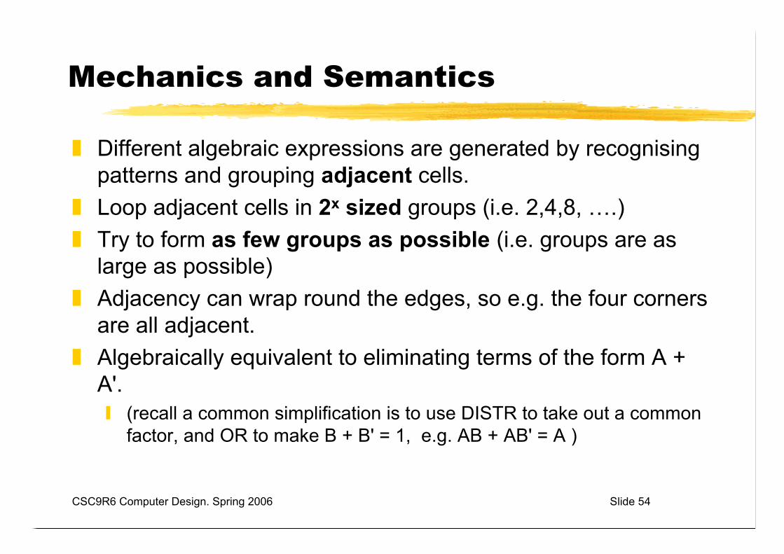
Mechanics and Semantics
Different algebraic expressions are generated by recognisingpatterns and grouping adjacent cells.
Loop adjacent cells in 2x sized groups (i.e. 2,4,8, ….) Try to form as few groups as possible (i.e. groups are as
large as possible) Adjacency can wrap round the edges, so e.g. the four corners
are all adjacent. Algebraically equivalent to eliminating terms of the form A +
A'. (recall a common simplification is to use DISTR to take out a common
factor, and OR to make B + B' = 1, e.g. AB + AB' = A )

CSC9R6 Computer Design. Spring 2006 Slide 55
Example 1
before grouping…
after grouping…
11 1 1
00 01 11 10
1
0
BCA
A positive
B positive
C positive
(confirm this by Boolean algebra)
CSC9R6 Computer Design. Spring 2006 Slide 56
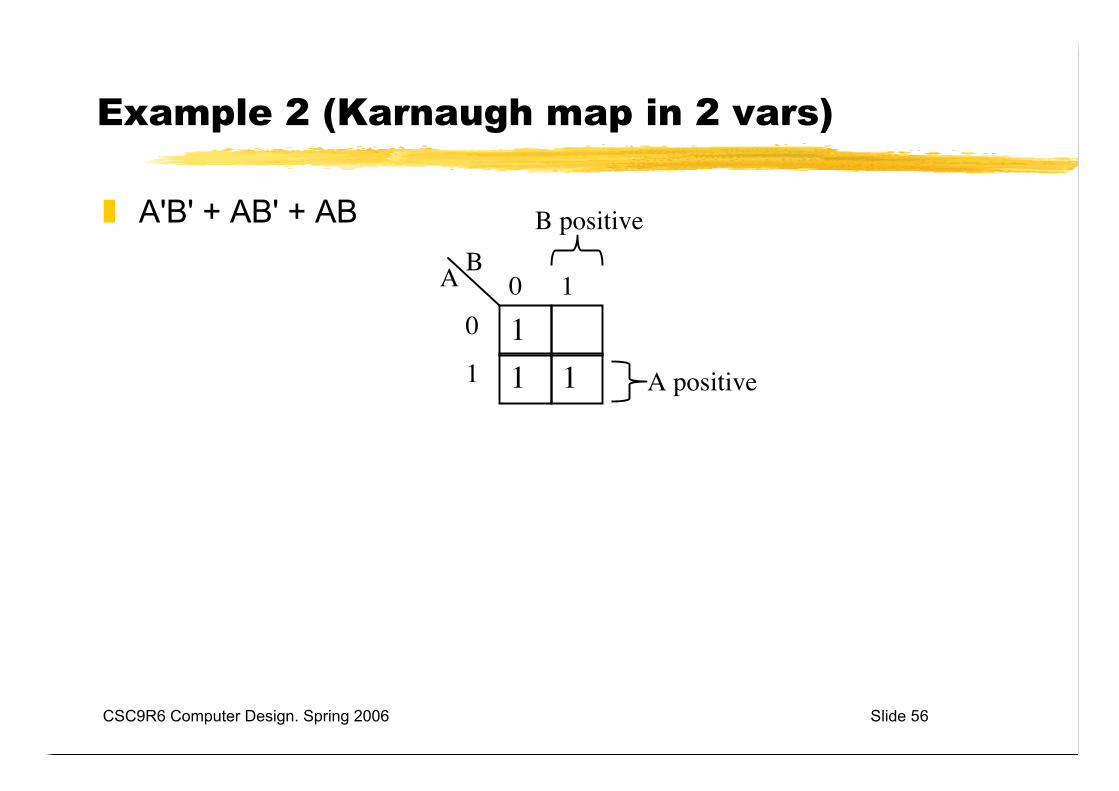
Example 2 (Karnaugh map in 2 vars)
A'B' + AB' + AB
11 1
0 1
1
0
BA
A positive
B positive

CSC9R6 Computer Design. Spring 2006 Slide 57
Example 3 (Karnaugh map in 4 vars)
A'B'C'D' + A'B'C'D + A'B'CD' + A'BC'D + ABC'D + AB'C'D' + AB'C'D +AB'CD'
A positive
1 11
100 01 11 10
CDAB
00
01
11
10
11 1 1
B positive
C positive
D positive

CSC9R6 Computer Design. Spring 2006 Slide 58
Sequential Logic Systems
The defining characteristic of a sequential logic system (SLS)is that the outputs of the system depend not only on thepresent inputs to the system, but also on the past history ofthe inputs and outputs of the system
i.e. SLSs have a form of memory.
CSC9R6 Computer Design. Spring 2006 Slide 59
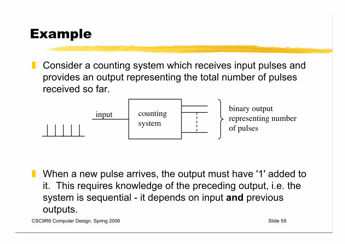
Example
Consider a counting system which receives input pulses andprovides an output representing the total number of pulsesreceived so far.
When a new pulse arrives, the output must have '1' added toit. This requires knowledge of the preceding output, i.e. thesystem is sequential - it depends on input and previousoutputs.
countingsystem
inputbinary outputrepresenting numberof pulses

CSC9R6 Computer Design. Spring 2006 Slide 60
SLS
The basic building block of the sequential logic system is theflip-flop. A typical scheme of an SLS is
The clock is included to control the flip flops - it ensures thatthe outputs change at certain instants of time, which may berequired to synchronise the SLS with other parts of the wholesystem.
combinationalcircuit
flip-flopsclock
inputs
outputs
CSC9R6 Computer Design. Spring 2006 Slide 61
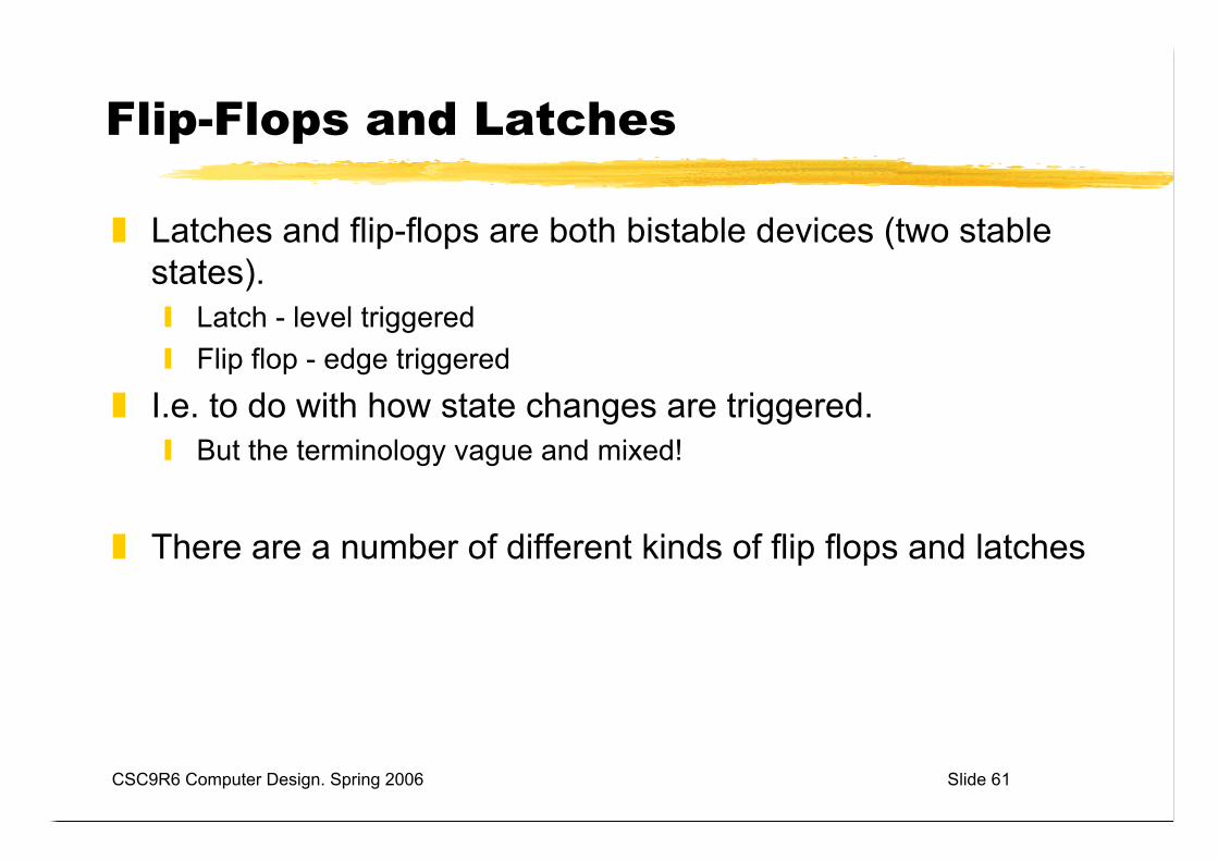
Flip-Flops and Latches
Latches and flip-flops are both bistable devices (two stablestates). Latch - level triggered Flip flop - edge triggered
I.e. to do with how state changes are triggered. But the terminology vague and mixed!
There are a number of different kinds of flip flops and latches

CSC9R6 Computer Design. Spring 2006 Slide 62
Set/Reset (S - R) latch
Broadly, S = 1 causes Q = 1, R = 1 causes Q = 0.
Q
R
S
Q'
CSC9R6 Computer Design. Spring 2006 Slide 63
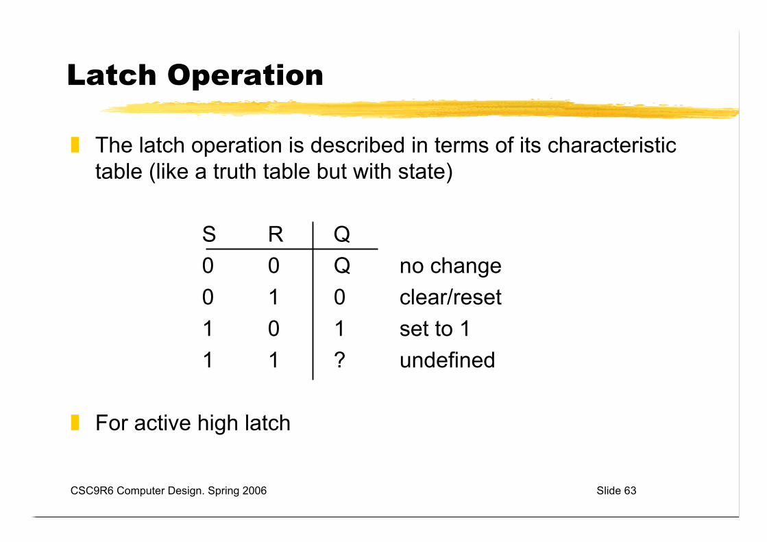
Latch Operation
The latch operation is described in terms of its characteristictable (like a truth table but with state)
S R Q0 0 Q no change0 1 0 clear/reset1 0 1 set to 11 1 ? undefined
For active high latch

CSC9R6 Computer Design. Spring 2006 Slide 64
Latch application
SR latch can also be used to combat switch debouncing. When a mechanical switch is opened or closed the contacts may
bounce and a dirty transition results (instead of a nice clean one).
results in clean transition - small bounces on S make nodifference to Q after initial 1.

CSC9R6 Computer Design. Spring 2006 Slide 65
S-R Gated Latch
Controlled by an enable.
If LOW enable signal then Q does not change, regardless ofvalues of S and R. Only when enable changes to HIGH canthe values of S and R be used to affect the output Q.
Steeringgates
latch
En1
3
2
4
CSC9R6 Computer Design. Spring 2006 Slide 66
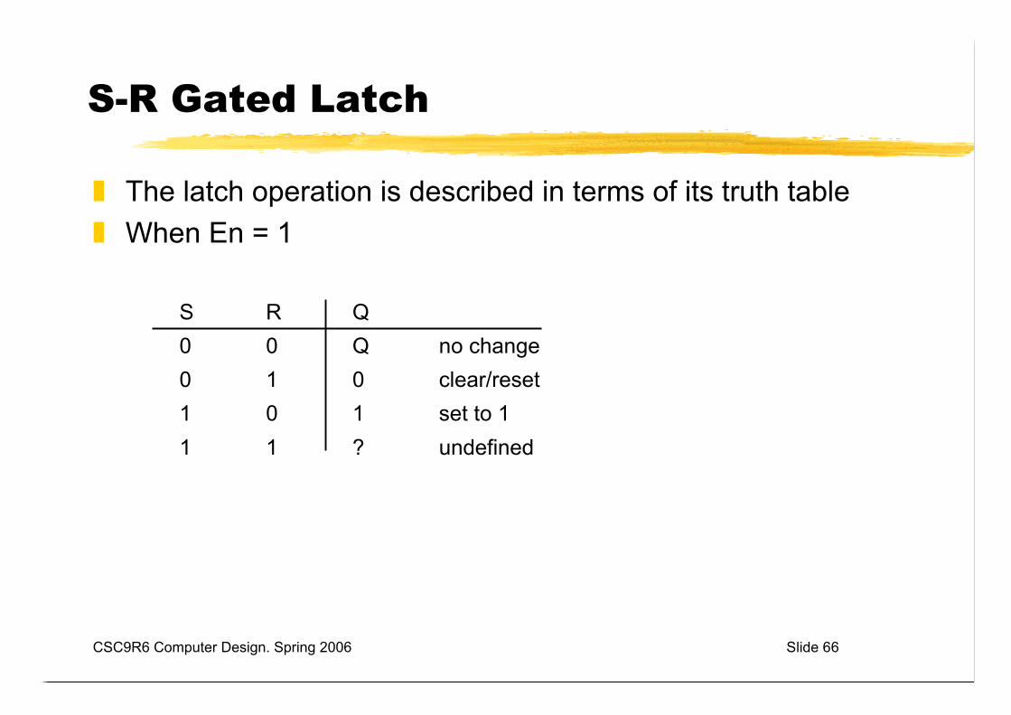
S-R Gated Latch
The latch operation is described in terms of its truth table When En = 1
S R Q0 0 Q no change0 1 0 clear/reset1 0 1 set to 11 1 ? undefined

CSC9R6 Computer Design. Spring 2006 Slide 67
S-R Gated Latch
The operation can also be seen by looking at the timing(waveform) diagram.
SREnQQ'
CSC9R6 Computer Design. Spring 2006 Slide 68
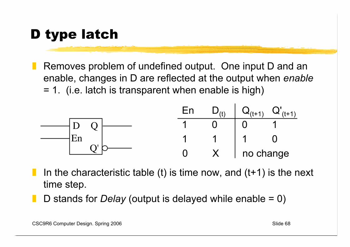
D type latch
Removes problem of undefined output. One input D and anenable, changes in D are reflected at the output when enable= 1. (i.e. latch is transparent when enable is high)
En D(t) Q(t+1) Q'(t+1)
1 0 0 1 1 1 1 0
0 X no change
In the characteristic table (t) is time now, and (t+1) is the nexttime step.
D stands for Delay (output is delayed while enable = 0)
QD
Q'En

CSC9R6 Computer Design. Spring 2006 Slide 69
D type latch
D = S and D' = R therefore never have S = R
1
3
2
4

CSC9R6 Computer Design. Spring 2006 Slide 70
Example: a register
Data D0 D0 …. D7 is loaded in parallel into the D latches on awrite signal.
The register may also include a special reset to clear allsimultaneously.
D0 D1 D7
Q0 Q1 Q7
write
DEn
Q DEn
Q DEn
Q...LSB MSB

CSC9R6 Computer Design. Spring 2006 Slide 71
Power Up
A system may contain a number of flip flops, counters, shiftregisters, etc.
What is their initial state immediately after power is applied? We need a known (and reproducible) state at power up, e.g.
flip-flops reset, counters zeroed, shift registers clears and soon.
Use a simple switch (interactive input) to reset all elementssimultaneously

CSC9R6 Computer Design. Spring 2006 Slide 72
Edge Detection
Problem: when enable = 1 the output varies depending on theinput. We might prefer that on the transition 0-1 the input issampled once and the output fixed, so changes of input arenot reflected until the next 0-1 transition.
Difference between a gated latch and a flip-flop is the use ofedge triggering. Flip-flop changes on 0-1 transition (or 1-0 transition) Latch changes on HIGH level (or LOW level)

CSC9R6 Computer Design. Spring 2006 Slide 73
Edge triggered flip flops
D flip flop
Rising edge triggered ie 0-1transition. Also clear and presetinputs.
The clock is dynamic input
JK flip flop
Falling edge triggered (1-0transition). Also clear and presetinputs.
CSC9R6 Computer Design. Spring 2006 Slide 74
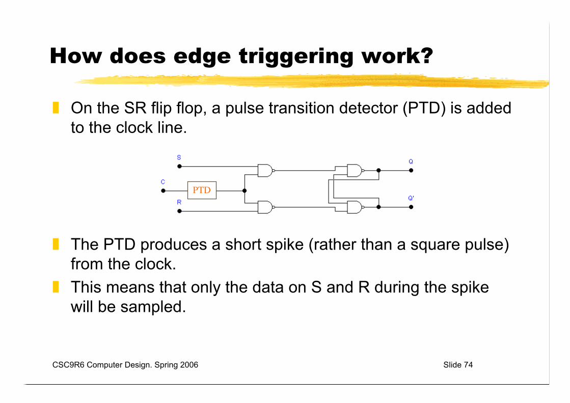
How does edge triggering work?
On the SR flip flop, a pulse transition detector (PTD) is addedto the clock line.
The PTD produces a short spike (rather than a square pulse)from the clock.
This means that only the data on S and R during the spikewill be sampled.
PTD

CSC9R6 Computer Design. Spring 2006 Slide 75
PTD
The Pulse Transition Detector is implemented by thefollowing gates.
Gates suffer from propagation delay; it takes time to changethe output to reflect new inputs.
Therefore, both C and C' will be high for a few nanoseconds. Sometimes propagation delay can be useful (as above) but
sometimes it just leads to (momentary) wrong answers. In clocked synchronous circuits all components are
guaranteed to change at the same instant.
delay spikeclock

CSC9R6 Computer Design. Spring 2006 Slide 76
Presentation of Data
Time constraints on presentation of data (for it to be reliably clocked intothe flip flop).
The set-up time is the minimum time between the leading edge of aninput data pulse and the triggering clock pulse.
The hold time is the time between the clock transition changing theoutput and the end of the input pulse. After the hold time the inputs maychange with no effect on the output.
The smaller these times the better. (e.g. setup times vary from 2 to 20 ns,hold times from 0.5 to 3 ns)
clock
input
setup time hold time
CSC9R6 Computer Design. Spring 2006 Slide 77
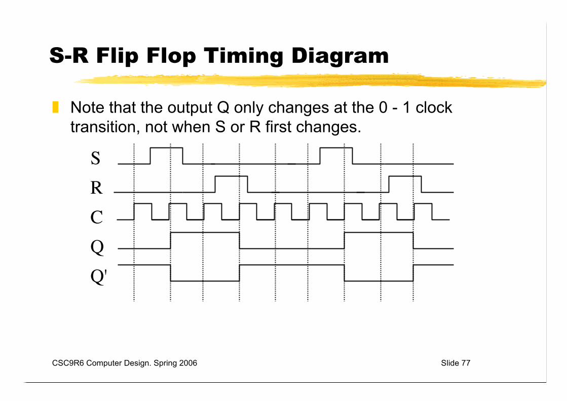
S-R Flip Flop Timing Diagram
Note that the output Q only changes at the 0 - 1 clocktransition, not when S or R first changes.
SRCQQ'

CSC9R6 Computer Design. Spring 2006 Slide 78
Propagation Delays
Consider the following circuit (R = A.B' + A'.C)
Let A = 1, B = 0, C = 1. What happens when A changes to 0? Logically the value of R should not change, but physically it
does.

CSC9R6 Computer Design. Spring 2006 Slide 79
Static Hazards
Let propagation delay of all gate be δ, and A changed at time t0
time A B C B' A' A.B' A'.C R< t0 1 0 1 1 0 1 0 1t0 0 0 1 1 0* 1* 0* 1*t0 + δ 0 0 1 1 1 0 0* 1*t0 + 2δ 0 0 1 1 1 0 1 0*t0 + 3δ 0 0 1 1 1 0 1 1
* means old values used - change has not yet propagated
These are called static hazards (when we have A and A') A hazard is likely if 2 adjacent cells in a Karnaugh map are not looped
together (may give larger terms, but eliminates hazard)

CSC9R6 Computer Design. Spring 2006 Slide 80
J - K Flip Flops
Another attempt to solve the problem of undefined output onthe SR latch (when S = R = 1)
J K Q(t+1)
0 0 Q(t) no change0 1 0 clear1 0 1 set1 1 Q(t)' toggle
like SR, but Q fed back to K gate, Q' back to J gate If J = K = 0 enabling does nothing If J ≠ K enabling causes Q(t+1) = J If J = K = 1 enabling causes toggle
CSC9R6 Computer Design. Spring 2006 Slide 81
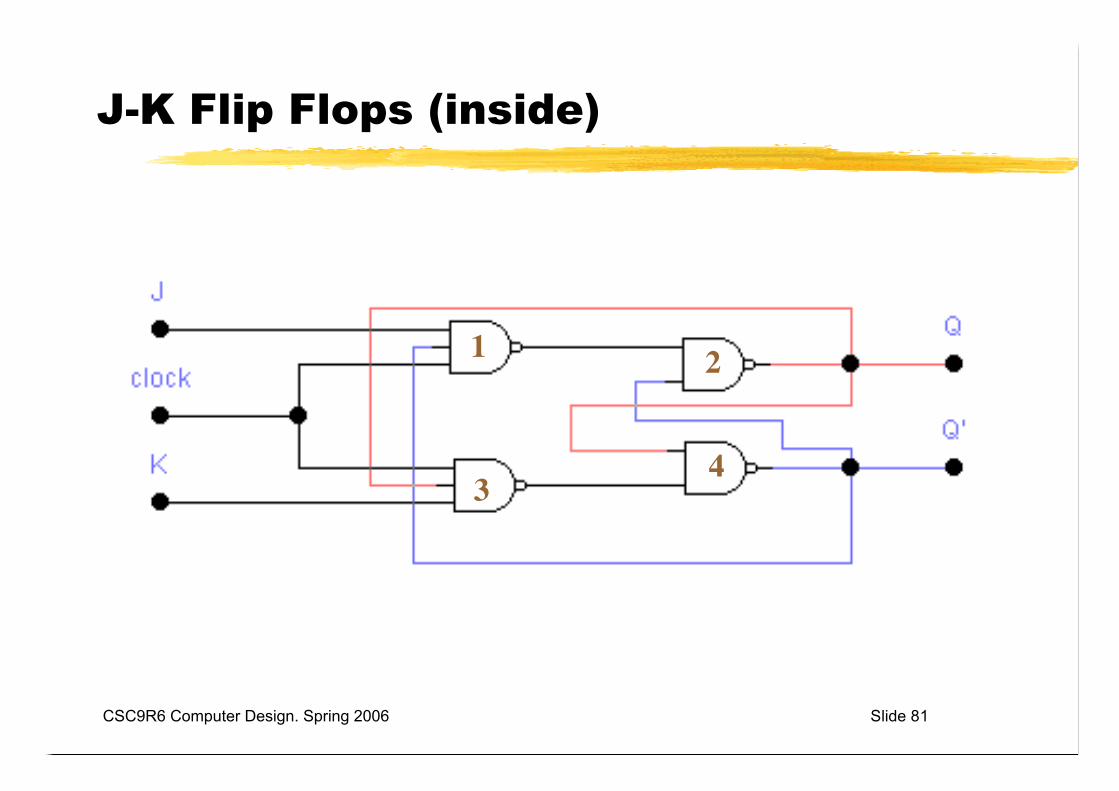
J-K Flip Flops (inside)
1
3
2
4

CSC9R6 Computer Design. Spring 2006 Slide 82
Example: Divide by 2
Q C0 00 11 01 1
J = K = 1 therefore the circuittoggles on the falling clock input.
The frequency of the outputwaveform is 1/2 that of the input(clock) waveform.
repeat
TQ = 2 x Tc
TQ
Tc
Q
C
time
CSC9R6 Computer Design. Spring 2006 Slide 83
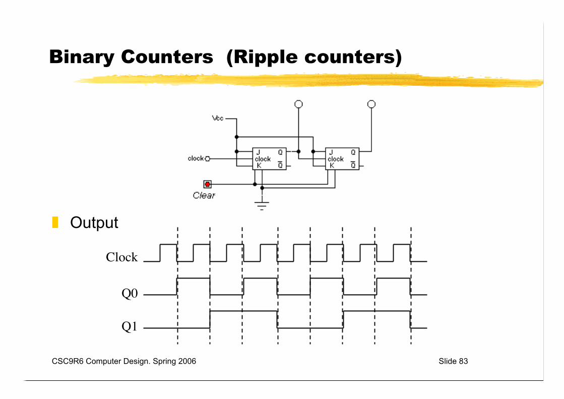
Binary Counters (Ripple counters)
Output
Clock
Q0
Q1

CSC9R6 Computer Design. Spring 2006 Slide 84
Binary Counters (Ripple counters)
Represent the output of the circuit as a table:Clock pulse number Q1 Q0
0 0 01 0 12 1 03 1 14 0 05 0 16 1 07 1 1
The system counts 4 clock pulses and then repeats. Counters for any number (2n) can be created by adding more J-K flip
flops. The Q output is connected to the clock input for the next stage.
counts 0,1, 2, 3
repeats
CSC9R6 Computer Design. Spring 2006 Slide 85
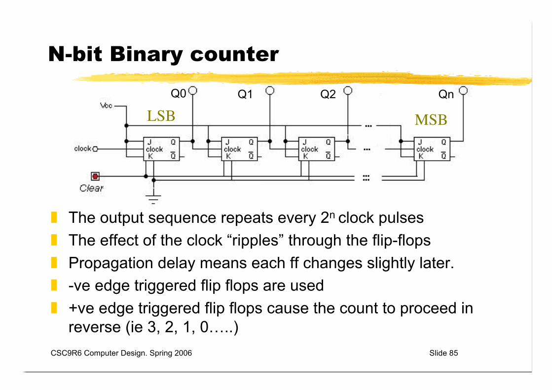
N-bit Binary counter
The output sequence repeats every 2n clock pulses The effect of the clock “ripples” through the flip-flops Propagation delay means each ff changes slightly later. -ve edge triggered flip flops are used +ve edge triggered flip flops cause the count to proceed in
reverse (ie 3, 2, 1, 0…..)
LSB MSB
Q0 Q1 Q2 Qn
CSC9R6 Computer Design. Spring 2006 Slide 86
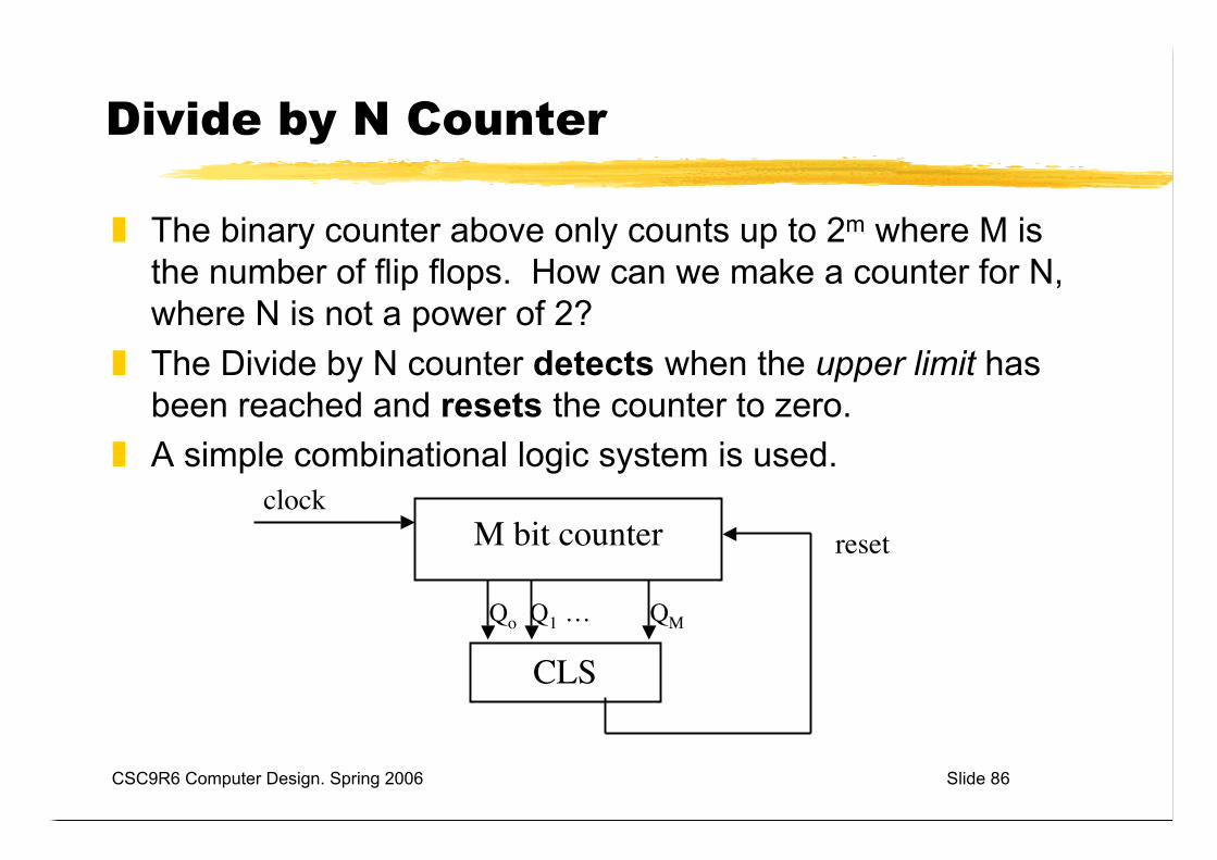
Divide by N Counter
The binary counter above only counts up to 2m where M isthe number of flip flops. How can we make a counter for N,where N is not a power of 2?
The Divide by N counter detects when the upper limit hasbeen reached and resets the counter to zero.
A simple combinational logic system is used.
Qo Q1 … QM
M bit counter
CLS
clockreset

CSC9R6 Computer Design. Spring 2006 Slide 87
Example: A decade counter
Decade counter counts from 0 to 9and repeats. Count sequence is
pulsenumber Q3 Q2 Q1 Q00 0 0 0 01 0 0 0 12 0 0 1 03 0 0 1 14 0 1 0 05 0 1 0 16 0 1 1 07 0 1 1 18 1 0 0 09 1 0 0 110 1 0 1 0
How many flip flops? 23 = 8, 24 = 16, therefore 4 flip
flops required.
Reset occurs when Q0 = 0, Q1 = 1, Q2 = 0, Q3 = 1
Assume clr is active high (ie 1 onclr means reset, 0 means donothing) and -ve edge triggered(1-0 transition)
Clr = (Q0' . Q1 . Q2' . Q3)
reset
CSC9R6 Computer Design. Spring 2006 Slide 88
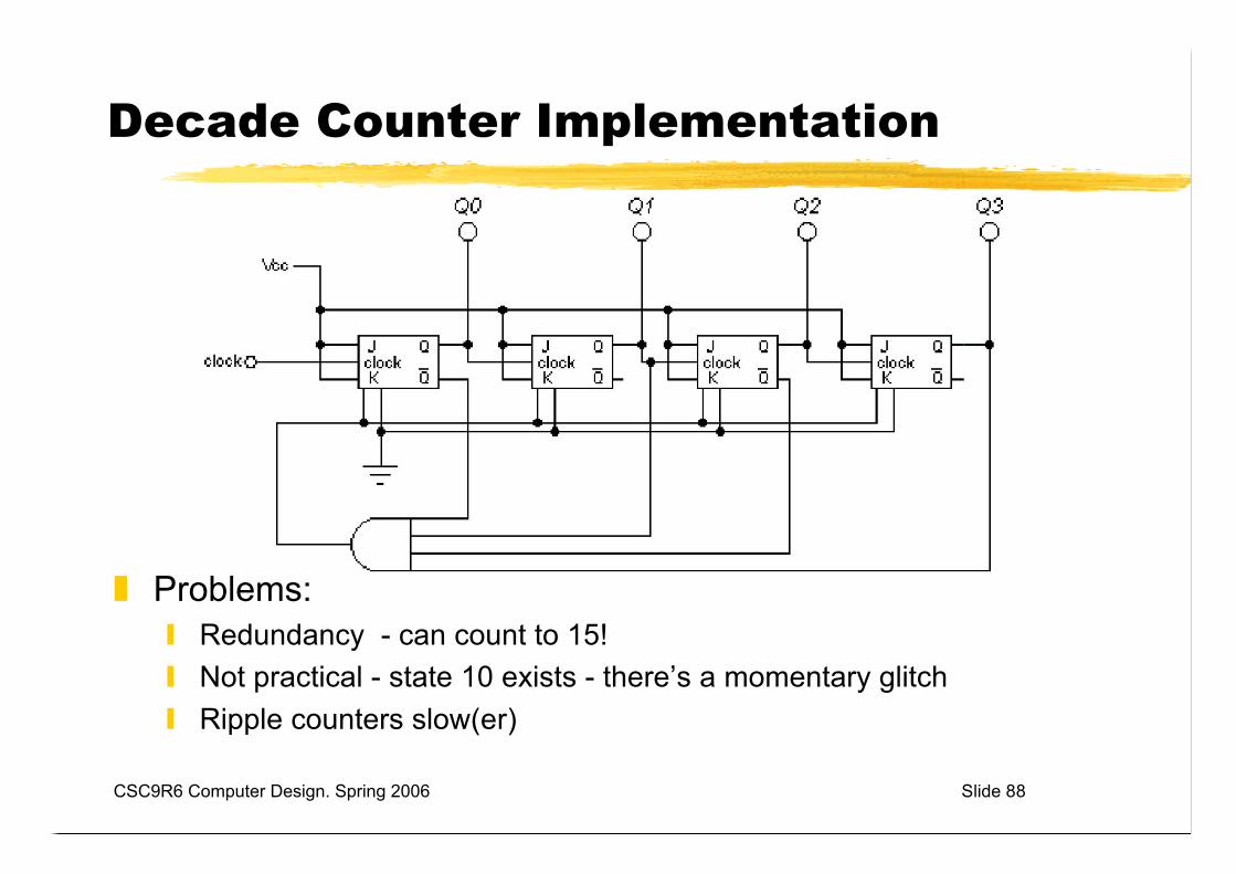
Decade Counter Implementation
Problems: Redundancy - can count to 15! Not practical - state 10 exists - there’s a momentary glitch Ripple counters slow(er)

CSC9R6 Computer Design. Spring 2006 Slide 89
Decade Counter Implementation
Problems: Redundancy - can count to 15! Not practical - state 10 exists - there’s a momentary glitch Ripple counters slow(er)
LSB MSB

CSC9R6 Computer Design. Spring 2006 Slide 90
Synchronous Counter
Consider clocking all flip flops at the same time.
How do we make the flip-flops toggle at the right time? Flip flop A toggles on every clock pulse Flip flop B toggles only when A is HIGH and there’s a clock pulse Flip flop C toggles only when A and B are HIGH and there’s a clock
pulse Flip flop D toggles only when A and B and C are HIGH and there’s a
clock pulse
A DCB
clock
1

CSC9R6 Computer Design. Spring 2006 Slide 91
Synchronous Counter: Implementation
The JK inputs come from previous Q inputs “anded” together.
How can this be altered to make a decade counter?
LSB MSB

CSC9R6 Computer Design. Spring 2006 Slide 92
Synchronous Decade Counter
More complicated arrangement to trigger each bit
LSB MSB

CSC9R6 Computer Design. Spring 2006 Slide 93
Synchronous Decade Counter
Recall the tablepulsenumber Q3 Q2 Q1 Q00 0 0 0 01 0 0 0 12 0 0 1 03 0 0 1 14 0 1 0 05 0 1 0 16 0 1 1 07 0 1 1 18 1 0 0 09 1 0 0 110 1 0 1 0 reset
Q1 triggers only on 1, 3, 5, 7 (but not 9)i.e. when Q1 is 1 but Q3 is 0
Q3 triggers only on 7 and 9
Q2 triggers only on 3 and 7i.e. when both Q1 and Q0 are 1