Karnaugh Maps & Combinational Logic Design
43
Karnaugh Maps & Combinational Logic Design ECE 152A – Winter 2012
Transcript of Karnaugh Maps & Combinational Logic Design

Karnaugh Maps & Combinational Logic Design
ECE 152A – Winter 2012

January 18, 2012 ECE 152A - Digital Design Principles 2
Reading Assignment
Brown and Vranesic 4 Optimized Implementation of Logic Functions
4.1 Karnaugh Map 4.2 Strategy for Minimization
4.2.1 Terminology 4.2.2 Minimization Procedure
4.3 Minimization of Product-of-Sums Forms 4.4 Incompletely Specified Functions 4.8 Cubical Representation
4.8.1 Cubes and Hypercubes

January 18, 2012 ECE 152A - Digital Design Principles 3
Reading Assignment
Roth 1 Introduction Number Systems and Conversion
1.4 Representation of Negative Numbers 1.5 Binary Codes
4 Applications of Boolean Algebra Minterm and Maxterm Expansions 4.5 Incompletely Specified Functions
January 18, 2012 ECE 152A - Digital Design Principles 4
Reading Assignment
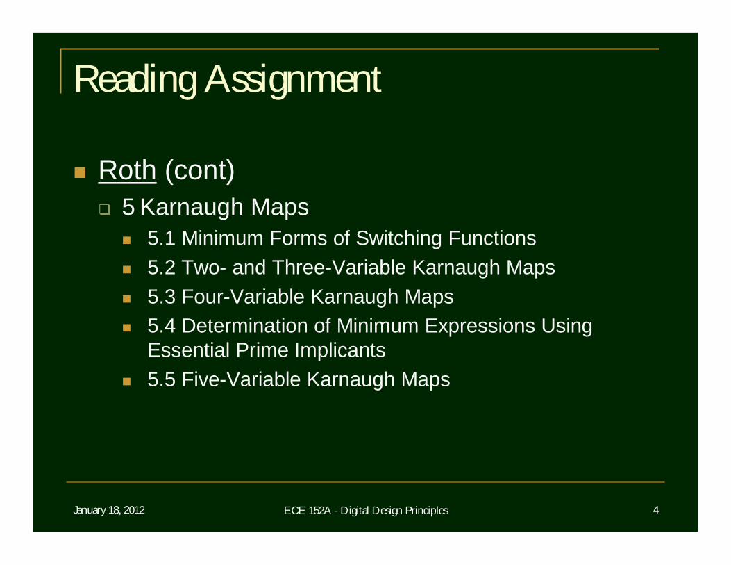
Roth (cont) 5 Karnaugh Maps
5.1 Minimum Forms of Switching Functions 5.2 Two- and Three-Variable Karnaugh Maps 5.3 Four-Variable Karnaugh Maps 5.4 Determination of Minimum Expressions Using
Essential Prime Implicants 5.5 Five-Variable Karnaugh Maps

January 18, 2012 ECE 152A - Digital Design Principles 5
Canonical Forms
The canonical Sum-of-Products (SOP) and Product-of-Sums (POS) forms can be derived directly from the truth table but are (by definition) not simplified Canonical SOP and POS forms are “highest cost”,
two-level realization of the logic function The goal of simplification and minimization is to
derive a lower cost but equivalent logic function

January 18, 2012 ECE 152A - Digital Design Principles 6
Simplification
Reduce cost of implementation by reducing the number of literals and product (or sum) terms Literals correspond to gate inputs and hence both
wires and the size (fan-in) of the first level gates in a two-level implementation
Product (Sum) terms correspond to the number of gates in the first level of a two-level implementation and the size (fan-in) of the second level gate

January 18, 2012 ECE 152A - Digital Design Principles 7
Simplification
Algebraic Simplification Using theorems and properties of Boolean
Algebra Difficult with large number of variables and complex
Boolean expressions Most often incorporated into CAD Tools
Karnaugh Maps Graphical representation of logic function suitable
for manual simplification and minimization

January 18, 2012 ECE 152A - Digital Design Principles 8
Two-Variable Karnaugh Map
Location of minterms and maxterms on a two-variable map Index is the same, expansion is complementary
0
1
0 1
m0 m1
m2 m3
AB
0
1
0 1
M0 M1
M2 M3
AB
January 18, 2012 ECE 152A - Digital Design Principles 9
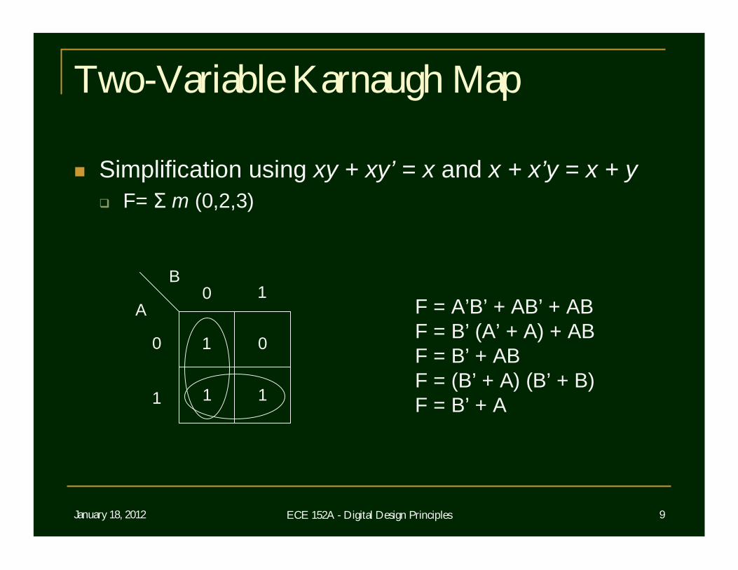
Two-Variable Karnaugh Map
Simplification using xy + xy’ = x and x + x’y = x + y F= Σ m (0,2,3)
0
1
0 1
01
A
B
11
F = A’B’ + AB’ + ABF = B’ (A’ + A) + ABF = B’ + ABF = (B’ + A) (B’ + B)F = B’ + A

January 18, 2012 ECE 152A - Digital Design Principles 10
Three-Variable Karnaugh Map
Location of three-variable minterms
0
1
00 01A
BC11 10
m4 m5 m7
m2m3m1m0
m6

January 18, 2012 ECE 152A - Digital Design Principles 11
Three-Variable Karnaugh Map
Adjacent cells differ in the value of only one variable Known as Gray coding Topological adjacency equates to algebraic
adjacency
000 → 001 → 011 → 010 ↑ ↓
100 ← 101 ← 111 ← 110

January 18, 2012 ECE 152A - Digital Design Principles 12
Three-Variable Karnaugh Map
Three Variable Sum-of-Products Simplification Groupings of 4 (22)
0
1
00 01A
BC11 10
00
0 0
1
11
1F = A’B’C’ + AB’C’ + A’BC’ + ABC’F = (A’ + A) B’C’ + (A’ + A) BC’F = B’C’ + BC’F = (B’ + B) C’F = C’

January 18, 2012 ECE 152A - Digital Design Principles 13
Three-Variable Karnaugh Map
Three Variable Product-of-Sums Simplification Groupings of 4 (22)
0
1
00 01A
BC11 10
00
0 0
1
11
1
A’+B+C’ A’+B’+C’
A+B’+C’A+B+C’
A+C’
A’+C’
F = C’

January 18, 2012 ECE 152A - Digital Design Principles 14
Four-Variable Karnaugh Map
Location of four-variable minterms
00
01
00 01AB
CD11 10
11
10
m4 m5 m7
m2m3m1m0
m6
m8 m9 m11
m14m15m13m12
m10

January 18, 2012 ECE 152A - Digital Design Principles 15
Four-Variable Karnaugh Map
Four-bit Gray code
0000 → 0001 → 0011 → 0010 ↓
0100 ← 0101 ← 0111 ← 0110↓
1100 →1101 → 1111 → 1110↓
1000 ← 1001 ← 1011 ← 1010

January 18, 2012 ECE 152A - Digital Design Principles 16
Four-Variable Sum-of-Products Map
00
01
00 01AB
CD11 10
11
10
0
00 0 0
1
0 1 0
1
1 1 1 1
11A
B’CDF = A + B’CD

January 18, 2012 ECE 152A - Digital Design Principles 17
Implementation with AND/OR/NOT & NAND gates

January 18, 2012 ECE 152A - Digital Design Principles 18
Four-Variable Product-of-Sums Map
00
01
00 01AB
CD11 10
11
10
0
00 0 0
1
0 1 0
1
1 1 1 1
11
(A + B’)
(A + C)(A + D)
F = (A + B’)(A + C)(A + D)

January 18, 2012 ECE 152A - Digital Design Principles 19
Algebraic conversion between SOP and POS forms Multiplying out
POS → SOP
F = (A + B’)(A + C)(A + D)
A + B’A + CAA + AB’
AC + B’CA + AB’ + AC + B’CA + B’CA + DAA + AB’C + AD + B’CD
F = A + B’CD
Factoring SOP → POS
F = A + B’CDF = (A + B’)(A + CD)
F = (A + B’)(A + C)(A + D)

January 18, 2012 ECE 152A - Digital Design Principles 20
Five-Variable Karnaugh Maps
00
01
00 01BC
DE11 10
11
10
1
1 1
1
1
00
01
00 01BC
DE11 10
11
10
11 1 1
1
1 1
11
A=0 A=1
1
B’CD’ BCDE
A’B’D’ AB’C

January 18, 2012 ECE 152A - Digital Design Principles 21
Six-Variable Karnaugh Map
00
01
00 01CD
EF11 10
11
10
AB=00
00
01
00 01CD
EF11 10
11
10
AB=10
00
01
00 01CD
EF11 10
11
10
AB=11
1 1
1 1
1 1
1 1
1 1
1 1 1 1
C’DF
00
01
00 01CD
EF11 10
11
10
AB=01
B’DF
ADF

January 18, 2012 ECE 152A - Digital Design Principles 22
Terminology
Literal An appearance of a variable or its complement
Implicant Any minterm and/or product term for which the
value of the function equals 1 (in SOP form) or any maxterm and/or sum term for which the value of the function equals 0 (in POS form)

January 18, 2012 ECE 152A - Digital Design Principles 23
Terminology
Prime Implicant An implicant that cannot be combined into another
implicant that has fewer literals Essential Prime Implicant A prime implicant that includes at least one
minterm not covered by any other prime implicant

January 18, 2012 ECE 152A - Digital Design Principles 24
Terminology
Cover A collection of implicants that accounts for
(covers) all minterms (or maxterms) for which a given function equals 1 in SOP form (or 0 in POS form)
Cost An heuristic figure of merit determined generally
from the number of product (sum) terms and the number of literals in a given cover
January 18, 2012 ECE 152A - Digital Design Principles 25
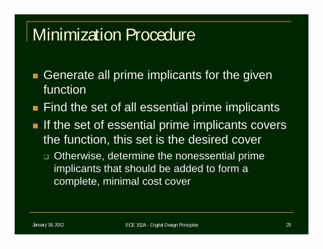
Minimization Procedure
Generate all prime implicants for the given function
Find the set of all essential prime implicants If the set of essential prime implicants covers
the function, this set is the desired cover Otherwise, determine the nonessential prime
implicants that should be added to form a complete, minimal cost cover

January 18, 2012 ECE 152A - Digital Design Principles 26
Minimization Example
00
01
00 01CD
11 10
11
10
0
0 0
1
1 0
1
1 1
11
1
11
0 0
10 Implicants (minterms)6 Prime Implicants
BC’, AB, AC,B’CD, A’B’D, A’C’D
2 Essential Prime ImplicantsBC’, AC
Final Cover with A’B’DF= A’B’D + BC’ + AC
AB

January 18, 2012 ECE 152A - Digital Design Principles 27
Combinational Logic Circuit Design
Specify combinational function using Truth Table, Karnaugh Map, or Canonical sum of minterms (product of maxterms)
This is the creative part of digital design Design specification may lend itself to any of the
above forms

January 18, 2012 ECE 152A - Digital Design Principles 28
Combinational Logic Circuit Design
Find minimal POS or SOP form of the logic function Technology can determine whether POS or SOP
is appropriate solution Nature of function and cost of implementation can
determine whether POS or SOP is better solution

January 18, 2012 ECE 152A - Digital Design Principles 29
Combinational Logic Circuit Design
Implement design using AND/OR (or NAND) gates or OR/AND (or NOR) gates In most technologies NAND and NOR
implementations are superior In terms of both size and speed
Simulate design and verify functionality and performance Design should always be verified before
committing to fabrication

January 18, 2012 ECE 152A - Digital Design Principles 30
Combinational Design Example 1
Design Specification Design a logic network that takes as its input a 4-
bit, one’s complement number and generates a 1 if that number is odd (0 is not odd) Label the inputs A, B, C and D, where A is the most
significant bit
Implement your design in standard sum-of-products representation using only NAND gates

January 18, 2012 ECE 152A - Digital Design Principles 31
Combinational Design Example 1
Recall representation of fixed-point, signed and unsigned numbers from ECE 15A (lecture #14)
-1-0-37111
-2-1-26110
-3-2-15101
-4-3-04100
3333011
2222010
1111001
0+0+00000
Two’s Complement
One’s Complement
Sign-Magnitude
UnsignedBinary

January 18, 2012 ECE 152A - Digital Design Principles 32
Design Example 1 – Truth Table
Odd, One’s complement numbers
01111
10111
01011
10011
01101
10101
01001
10001
11110
00110
11010
00010
11100
00100
11000
00000
FDCBA

January 18, 2012 ECE 152A - Digital Design Principles 33
Design Example 1 – Karnaugh Map
00
01
00 01CD
11 10
11
10
0
1
1 0
1
1
0 0
AB
0 1 01
1 10 0
F = A’D + AD’

January 18, 2012 ECE 152A - Digital Design Principles 34
Incompletely Specified Functions
Some logic functions have input combinations that can never occur Examples:
Sensors indicating a mutually exclusive event has occurred
Processor flags indicating a result was both positive and negative
Interlocked switches that can never be closed at the same time

January 18, 2012 ECE 152A - Digital Design Principles 35
Incompletely Specified Functions
Conditions called “don’t cares” For minterms/maxterms associated with “don’t
care” input combinations, assign output value of 0 or 1 to generate the minimum cost cover
On Karnaugh Map, represent “don’t cares” with X and group with minterms (maxterms) to create prime implicants Any X’s not covered can be ignored and will default to 0
(in SOP form) or 1 (in POS form)

January 18, 2012 ECE 152A - Digital Design Principles 36
Design Example 2
Design Specification Design a combinational circuit that takes as its
input a Binary Coded Decimal (BCD) digit (four bits) and outputs a 1 if the input is an even number (not zero)
Recall Binary Coded Decimal representation from ECE 15A Not most economical representation
10 valid combinations per 4 bits 100 valid combinations per byte

January 18, 2012 ECE 152A - Digital Design Principles 37
Design Example 2
BCD Example
X111170111X111060110X110150101X110040100X101130011X10102001091001100018100000000
ValueBCDValueBCD

January 18, 2012 ECE 152A - Digital Design Principles 38
Design Example 2
Canonical Forms for Incompletely Specified Functions For design example, function determined directly
from design specification Even numbers, not 0
)15,14,13,12,11,10()9,7,5,3,1,0(
)15,14,13,12,11,10()8,6,4,2(
dM
dm

January 18, 2012 ECE 152A - Digital Design Principles 39
Design Example 2 – SOP Karnaugh Map
00
01
00 01CD
11 10
11
10
0 10
1
AB
0
X
01
1 0
0
X
XXXXF = BD’ + AD’ + CD’

January 18, 2012 ECE 152A - Digital Design Principles 40
Design Example 2 – POS Karnaugh Map
00
01
00 01CD
11 10
11
10
0 10
1
AB
0
X
01
1 0
0
X
XXXXF = D’ (A + B + C)

January 18, 2012 ECE 152A - Digital Design Principles 41
Design Example 3
Design Specification In this problem, you are to design the combinational circuit
that controls the ceiling lights in my downstairs hallway There are three wall switches: one at the front door (A),
one at the back door (B) and one in the family room (C) When I walk in the front door, the ceiling lights are off, the
A switch is ON and both the B and C switches are OFF From these initial conditions, changing the position of any
switch should turn the lights on; changing the position of any switch (again) should turn the lights off, etc.
January 18, 2012 ECE 152A - Digital Design Principles 42
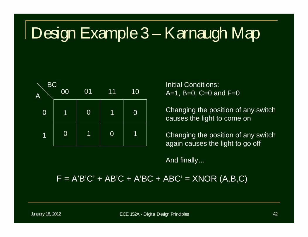
Design Example 3 – Karnaugh Map
0
1
00 01A
BC11 10
00
0 0
1
11
1
Initial Conditions:A=1, B=0, C=0 and F=0
Changing the position of any switchcauses the light to come on
Changing the position of any switchagain causes the light to go off
And finally…
F = A’B’C’ + AB’C + A’BC + ABC’ = XNOR (A,B,C)
January 18, 2012 ECE 152A - Digital Design Principles 43
Design Example Review
From Design Specification to Implementation: Example 1
Generate truth table from specification Example 2
Generate sum of minterms (product of maxterms) from specification
Example 3 Generate Karnaugh map from specification