Journal of Crystal Growth - Qing Pengqpeng.org/publication/pdf/Peng_2016_JCG_AlN.pdf · Properties...
8
Properties of AlN film grown on Si (111) Yiquan Dai a , Shuiming Li a,b,c , Qian Sun b,c , Qing Peng d,e , Chengqun Gui d , Yu Zhou b,c , Sheng Liu d,n a Mechanical Science & Engineering, Huazhong University of Science & Technology, Wuhan 430074, China b Key Laboratory of Nanodevices and Applications, Chinese Academy of Sciences (CAS), Suzhou 215123, China c Suzhou Institute of Nano-Tech and Nano-Bionics (SINANO), Chinese Academy of Sciences (CAS), Suzhou 215123, China d School of Power and Mechanical Engineering, Wuhan University, Wuhan, Hubei 430072, China e Department of Mechanical, Aerospace and Nuclear Engineering, Rensselaer Polytechnic Institute, Troy, NY 12180, USA article info Article history: Received 9 June 2015 Received in revised form 13 November 2015 Accepted 18 November 2015 Communicated by C. Caneau Available online 26 November 2015 Keywords: A1. Characterization A1. X-ray microdiffraction A3. Metalorganic chemical vapor deposition B1. Nitride B2. Semiconductor III–V materials B2. Piezoelectric materials abstract Stress and strain in an AlN film grown on Si (111) substrate have been evaluated by measuring Raman frequency shifts. Mechanical properties and phonon deformation potentials of AlN are evaluated by first principles calculations. The calculation model is verified by comparing the calculated Raman frequencies and frequencies detected from a bulk single crystal. Results show that the two sets of frequencies agree very well with each other. Thus, with the same verified model and parameters, elastic constants and phonon deformation potentials are calculated. Additionally, we successfully develop a numerical model to verify the calculation above and the model itself is also useful to predict properties of crystal films. Finally, the stress, strain, and piezoelectric properties are analyzed and compared for films on different substrates. & 2015 Elsevier B.V. All rights reserved. 1. Introduction Aluminum nitride (AlN) is an attractive candidate material for semiconductor applications [1], such as acoustic wave devices, UV solid-state light sources, MIS (metal–insulator– semiconductor) devices, and as a buffer-layer for gallium nitride (GaN). Though these exciting applications have been reported for years, there are still many problems due to lattice and thermal mismatch [2,3]. Large misfits between films and sub- strates lead to a high dislocation density, even cracking [4]. In order to deal with this problem, different film growth technol- ogies, mechanical characterizations, and growth parameter optimizations have been developed [5]. Furthermore, the stress state of a film is strongly correlated to the reliability of the metal line interconnection in devices and the percentage of disloca- tions in post thermal processing [6]. Directly measuring the strain state of these nitride films or microscale semiconductors is one of the potential techniques used for reliability characterization. In terms of stress/strain measurement, Raman scattering is a very convenient non-destructive stress detection method, espe- cially for materials or electronic devices bearing unknown loading corresponding to intrinsic phonon frequency shifts. Moreover, Raman active phonons are straightforward signatures of bonds within a sample's mixed phase and bonds at interfaces, by which the quality of film crystallization and its in-situ evolution can also be characterized [7]. Currently, its utility in III-V nitride com- pounds mainly depends on the elastic constants' determination and phonon deformation potential (PDP) calibration [8–11]. (PDP is defined as the (constant) coefficient between the Raman fre- quency shift and strain or stress quantization [8]). First principles calculations are one of the effective ways to rebuild Raman frequencies [12,13], based on which elastic con- stants [14–16] and phonons [17–19] can be analyzed theoretically. From recent publications [20–22], and early articles [14,15], one can find comparisons on AlN, which show some fluctuation in results. Most of the calculations are compared or verified just by other calculations, lacking independent theoretical or experi- mental support. For example, the authors in references [9–10,23] confuse whose elastic constants are the best and even calculate several sets of PDP based on different elastic constants. At the same time, the inconsistency of PDP appearing in literature also Contents lists available at ScienceDirect journal homepage: www.elsevier.com/locate/jcrysgro Journal of Crystal Growth http://dx.doi.org/10.1016/j.jcrysgro.2015.11.016 0022-0248/& 2015 Elsevier B.V. All rights reserved. n Corresponding author. E-mail address: [email protected] (S. Liu). Journal of Crystal Growth 435 (2016) 76–83
Transcript of Journal of Crystal Growth - Qing Pengqpeng.org/publication/pdf/Peng_2016_JCG_AlN.pdf · Properties...
Journal of Crystal Growth 435 (2016) 76–83
Contents lists available at ScienceDirect
Journal of Crystal Growth
http://d0022-02
n CorrE-m
journal homepage: www.elsevier.com/locate/jcrysgro
Properties of AlN film grown on Si (111)
Yiquan Dai a, Shuiming Li a,b,c, Qian Sun b,c, Qing Peng d,e, Chengqun Gui d,Yu Zhou b,c, Sheng Liu d,n
a Mechanical Science & Engineering, Huazhong University of Science & Technology, Wuhan 430074, Chinab Key Laboratory of Nanodevices and Applications, Chinese Academy of Sciences (CAS), Suzhou 215123, Chinac Suzhou Institute of Nano-Tech and Nano-Bionics (SINANO), Chinese Academy of Sciences (CAS), Suzhou 215123, Chinad School of Power and Mechanical Engineering, Wuhan University, Wuhan, Hubei 430072, Chinae Department of Mechanical, Aerospace and Nuclear Engineering, Rensselaer Polytechnic Institute, Troy, NY 12180, USA
a r t i c l e i n f o
Article history:Received 9 June 2015Received in revised form13 November 2015Accepted 18 November 2015
Communicated by C. Caneauvery well with each other. Thus, with the same verified model and parameters, elastic constants and
Available online 26 November 2015
Keywords:A1. CharacterizationA1. X-ray microdiffractionA3. Metalorganic chemical vapor depositionB1. NitrideB2. Semiconductor III–V materialsB2. Piezoelectric materials
x.doi.org/10.1016/j.jcrysgro.2015.11.01648/& 2015 Elsevier B.V. All rights reserved.
esponding author.ail address: [email protected] (S. Liu).
a b s t r a c t
Stress and strain in an AlN film grown on Si (111) substrate have been evaluated by measuring Ramanfrequency shifts. Mechanical properties and phonon deformation potentials of AlN are evaluated by firstprinciples calculations. The calculation model is verified by comparing the calculated Raman frequenciesand frequencies detected from a bulk single crystal. Results show that the two sets of frequencies agree
phonon deformation potentials are calculated. Additionally, we successfully develop a numerical modelto verify the calculation above and the model itself is also useful to predict properties of crystal films.Finally, the stress, strain, and piezoelectric properties are analyzed and compared for films on differentsubstrates.
& 2015 Elsevier B.V. All rights reserved.
1. Introduction
Aluminum nitride (AlN) is an attractive candidate materialfor semiconductor applications [1], such as acoustic wavedevices, UV solid-state light sources, MIS (metal–insulator–semiconductor) devices, and as a buffer-layer for gallium nitride(GaN). Though these exciting applications have been reportedfor years, there are still many problems due to lattice andthermal mismatch [2,3]. Large misfits between films and sub-strates lead to a high dislocation density, even cracking [4]. Inorder to deal with this problem, different film growth technol-ogies, mechanical characterizations, and growth parameteroptimizations have been developed [5]. Furthermore, the stressstate of a film is strongly correlated to the reliability of the metalline interconnection in devices and the percentage of disloca-tions in post thermal processing [6]. Directly measuring thestrain state of these nitride films or microscale semiconductorsis one of the potential techniques used for reliabilitycharacterization.
In terms of stress/strain measurement, Raman scattering is avery convenient non-destructive stress detection method, espe-cially for materials or electronic devices bearing unknown loadingcorresponding to intrinsic phonon frequency shifts. Moreover,Raman active phonons are straightforward signatures of bondswithin a sample's mixed phase and bonds at interfaces, by whichthe quality of film crystallization and its in-situ evolution can alsobe characterized [7]. Currently, its utility in III-V nitride com-pounds mainly depends on the elastic constants' determinationand phonon deformation potential (PDP) calibration [8–11]. (PDPis defined as the (constant) coefficient between the Raman fre-quency shift and strain or stress quantization [8]).
First principles calculations are one of the effective ways torebuild Raman frequencies [12,13], based on which elastic con-stants [14–16] and phonons [17–19] can be analyzed theoretically.From recent publications [20–22], and early articles [14,15], onecan find comparisons on AlN, which show some fluctuation inresults. Most of the calculations are compared or verified just byother calculations, lacking independent theoretical or experi-mental support. For example, the authors in references [9–10,23]confuse whose elastic constants are the best and even calculateseveral sets of PDP based on different elastic constants. At thesame time, the inconsistency of PDP appearing in literature also
Y. Dai et al. / Journal of Crystal Growth 435 (2016) 76–83 77
puzzles us and others [11] as to which is the most accurate. In fact,these problems have been noticed by Callsen et al. [8] andŁepkowski [20], which reveal some elastic constants are sensitiveto Raman frequency shifts or calculation methods. This is worthfurther study or clarification aimed for comparison of detectedRaman and calculated frequencies, and then, using this Ramanverified model to estimate the elastic constants and PDP.
Therefore, we prepare good quality films to investigate theproblems mentioned above. Firstly, we characterize the sampleswith XRD (X-ray diffraction) and Raman scattering. Secondly, weexplore parameters to rebuild Raman frequencies and comparethem with single bulk crystal (stress free) experiment and thenuse this Raman verified model and the same parameters to cal-culate elastic constants and PDP. The relationship between thetwo calculations is discussed in detail. Thirdly, the results ofelastic constants and PDP are verified further by Finite ElementModeling (FEM) simulations of the sample's state. At the sametime, the constructed FEM model is also a new way to forecastthe crystal film stress and piezoelectric properties. At last, thestress/strain and piezoelectric properties in films grown on dif-ferent substrates reported recently are evaluated together forcomparison.
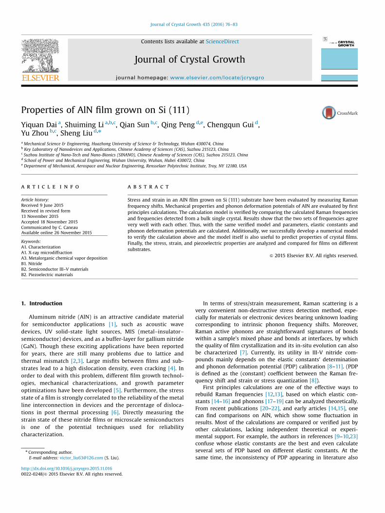
Fig. 1. XRD patterns and sample information. (a) XRD profiles of the AlN thin film. (b) Rroughness is 0.25 nm.
2. Experiment detail
2.1. Sample preparation
The samples of AlN on silicon (111) are grown by MOCVD(Metal-Organic Chemical Vapor Deposition). Trimethylaluminumand ammonia are used as precursors for aluminum and nitrogenrespectively, with hydrogen as the carrier gas. 2-in. silicon (111)wafers are loaded into the reactor through a N2 filled glove boxand the temperature is raised to 950 °C for thermal cleaning andremoval of native oxide. Al pre-seeding is performed after sub-strate preparation and a 200 nm thick AlN epitaxial layer is grownat 1150 °C. The V/III ratio is controlled at 1100 with a pressure of100 mbar during growth. The AFM inspection and characterizationwith XRD and Raman scattering are carried out after cooling toroom temperature. However, just during this cooling process,stresses/strains are introduced due to TEC (Thermal ExpansionCoefficient) mismatch between substrate and film, see Fig. 3.
2.2. XRD analysis
In the x-ray two-theta scan (Fig. 1a), the (0002) AlN peak showsa FWHM (Full Width at Half Maximum) of about 0.175°. This
ocking curve around (0002) reflection. (c) AFM scans of 5 mm�5 mm�10 nm. RMS

Y. Dai et al. / Journal of Crystal Growth 435 (2016) 76–8378
indicates a well-defined c-axis oriented wurtzite AlN [24]. Com-paring the rocking curve (Fig. 1b) with recent studies in literature[25–28], see Table 1, our samples present the lowest value ofFWHM, which implies a higher crystal quality. In addition, thesurface morphology characterized by AFM (Fig. 1c) also indicates aflat and smooth film. This is consistent with the smaller FWHMvalue of the rocking curve which is an indicator of dislocationdensity [26]. In fact, there would be a lot of hexagonal pits on thesurface of the film if the growth conditions are not optimal, as hasbeen observed and verified in our previous work [29].
Commonly, lattice parameters are used as datum for straincharacterization and X-ray diffraction is one of the ways to recordthe variation of the lattice. However, it is more difficult to deter-mine a-lattice length than c-lattice length especially for thinsamples like the film in this paper [24] (see page10 of Ref. [24]).Raman scattering is more convenient for quantitative detection forsuch a film.
Table 1Crystal quality comparison (omega scans).
Ref. FWHM of (0002) Film thickness (nm)
[25] 1° 200[26] 1.2° Unknown[27] 0.68° 380[28] 0.6° 300Present 0.259° 200
Fig. 2. Raman frequencies (Resolution of Raman scan is 0.4 cm�1). (a) Raman shift of silalong diameter. (d) Enlargement of Ehigh2 of interior points.
2.3. Raman analysis
Space group information of AlN's wurtzite structure has beenpublished in the literature [30]. In practice, the frequency shift ofEhigh2 is often used to detect stress/strain in III-nitride compounds,even in-situ monitoring of the film growth [7]. We choose back-scattering geometry with the laser beam incident on the (0001)surface. According to [30], only E2 and A1ðTOÞ are allowed to thedetector in this mode. This is the only suitable geometry mode fora thin film with a dark substrate for in-situ monitoring, and avoidsthe influence of E1ðTOÞ (e.g., see the stronger E1ðTOÞ near Ehigh2 asshown in [31]). A confocal micro-Raman scattering setup (LabRAMHR800, Laser length: λ¼ 5327Δλ nm , Δλr0:65 nm; diameterof laser: �1 μm) is used to accomplish the experiment at roomtemperature (12 °C). As can be seen in Fig. 2, we have performedRaman scatterings on 6 points along the diameter of the wafer'ssurface, see Fig. 2b. However, the trend of Ehigh2 along the radius isnot obvious. The values of FWHM and peak positions show a littlefluctuation for most of the interior points. The spectrums of edgepoints (less than 2 mm to the edge) become relatively weak.
FWHM line-width in Raman spectra is widely recognized as aninversely proportional indication of phonon lifetime, and highercrystal quality is associated with longer lifetime [31]. According tothis, the bulk crystal from Ref. [32] is the best single crystal amongthese carefully selected references and its frequencies will be usedas benchmark frequencies and stress free datum. It is well knownthat the film's stress due to TEC mismatch will degrade the crystalquality [28]. Therefore, the FWHM line-width is a useful indicator
icon wafer. (b) Schematic of Raman scattering points. (c) Raman scattering at points

Table 3Raman frequencies from experiments and calculations (cm�1).
low A1ðTOÞ high E1ðTOÞ
Table 2Comparison with other Raman experiments (cm�1).
Ref. Ehigh2 ΔωðEhigh2 Þ More info
[32] 657 0 Bulk crystal, FWHM(Ehigh2 )o3.8 cm�1
[33] 656 �1 Bulk crystal, FWHM(Ehigh2 )E6.6 cm�1
[17] 655.5 �1.5 Bulk crystal[34] 657.42 0.42 Film, substrate: Sapphire[35] 656.3 �0.7 Film, substrate: SiC[36] 655 �2.0 Film, substrate: Si (001)[37] 649 �8.0 Film, substrate: Si (111)Present 649.9 �7.1 Film, substrate: Si (111)
The value of Present is estimated from Fig. 2 and the uncertainty in stress can alsobe estimated further by comparing the range of Ehigh2 (649.8–650.5 cm�1 in Fig. 2d)with 657 cm�1 of bulk crystal [32].
Y. Dai et al. / Journal of Crystal Growth 435 (2016) 76–83 79
for crystal quality comparison, which we have adopted in ourMOCVD to monitor whether the crystal quality is improved after achange in the growth conditions [29]. As can be seen, our FWHMline-width is around 7 cm�1 which is very close to the singlecrystal's value, 6.6 cm�1 [33]. As mentioned above, the film'sstress can be identified as being proportional to the difference ofΔωðEhigh2 Þ between the film and single crystal of [32].
Theoretically, the surface of the sample is under biaxial stress,which means the stress tensor σz¼0. According to Ref. [8], thefrequency shift for each phonon mode is determined by thedeformation potential constants ~a and ~b for a given stress:
Δω¼ 2 ~aσxþ ~bσz ð1ÞThe mechanical reliability can be analyzed with the value of ~a
to calculate the stress, given σz¼0 in a film. However, it is notenough to investigate piezoelectric properties and the elasticconstants should also be clarified for piezoelectric tensordetermination.
We have observed that the values of FWHM of Raman spectrathat appeared in literature are different and this means the qua-lities of the crystals are different. Specially, the Raman shift causedby this crystal quality degradation is difficult to evaluate. Forexample, the values of Ehigh2 are not identical, even when com-paring only data for bulk crystals (see Table 2). Therefore, theforecast precision of this paper is based on high quality crystals.
E2 E2
[32] 611 657 671 Bulk[33] 609.6 656 669.3 Bulk[17] 247.5 608.5 655.5 669.3 Bulk[19] 248.4 613.8 660 673.4 Film 6 K[19] 248.6 611.0 657.4 670.8 Film 300 KCalculated 247.23 608.08 647.35 662.08 P¼�1.5 GPaCalculated 247.30 615.60 656.52 670.48 P¼0 GPaCalculated 247.34 623.09 665.60 678.80 P¼1.5 GPaCalculated 0.037 5.003 6.083 5.573 �ð2 ~aþ ~bÞ[8] 0.75 1.46 1.66 1.20 � ~bCalculated �0.713 3.543 4.423 4.373 �2 ~a
The records of [19] are AlN films on α-Al2O3 substrate at 6 K and 300 K. Hydrostaticpressure Po0 means being stretched.
Table 4Elastic constants from experiments and calculations (GPa).
C11 C12 C13 C33 C44 C E γzx
[45] 411 149 99 389 125 509.6 346.1 0.1768[46] 410.5 148.4 98.9 384.3 124.0 508.0 345.8 0.1770Calculated 411.2 125.9 92.2 404.0 125.7 495.0 361.9 0.1717
C ¼ C11þC12�2C213
C33; σx ¼ Cεx; γzx ¼ C13
C11 þC12[14,15]; Cij: Elastic constant; γzx: Poisson
ratio; σ: Stress tensor; ε: Strain tensor; E: Young's modulus; the rightmost threecolumns, C, E and γzx are calculated here.
3. Calculations
3.1. Calculation methods and their relationship
The calculations are performed within the framework of den-sity function theory. The GGA (generalized gradient approxima-tion) functional PW91 (Perdew-Wang1991) [38] is adopted torealize an approximation of the electronic subsystem. At the sametime, we selected norm-conserving pseudo-potentials [39] but notultra-soft potentials, which are commonly adopted in similar cal-culations. Ultra-soft potentials allow the calculation to run with alower energy cut-off than norm-conserving pseudo-potentials,which in turn saves much calculation time and has drawn muchattention from investigators [40]. However, it is more complex andmay not give a good expression in linear response calculations inour case [41].
Specifically, Raman spectra are calculated by a hybrid finitedisplacement/density perturbation theory (DFPT) method (alsonamed Linear Response method) [42]. In summary, the DFPTproblem is solved by minimizing the second order perturbation inthe total energy, which gives the first order changes in density,wave functions, and potential [42]. The main idea to determine theelastic constants [14,15] is to set a finite value as stress/strain and
then calculate the corresponding strain/stress after re-minimizingthe total energy. As mentioned above, the two calculations havesome intrinsic relationship all based on total energy with secondorder or first order derivation. In fact, the phonon spectrum fromRaman scattering is one of the fundamental indicators for crystaldynamics, which is strongly correlated to elastic constants [43].Obviously, it is reasonable to take rebuilding of Raman frequenciesas verification of the model used to calculate elastic constants.
In the calculation model, atom-site information of the primitivecell is from ICSD#41482 [44] and the lattice parameters area¼3.11, c¼4.98, and u¼0.382. After relaxation, the lattice para-meters are changed to be a¼3.073, c¼4.948, and u¼0.381. TheMonkhorst-Pack k-point grids are 11�11�11 for Brillouin-zonesampling. Kinetic cut-off energies for the plane wave expression ofthe wave function are set at 1600 eV.
3.2. Results and comparison
The calculation results under different hydrostatic pressureshave been listed in Table 3 together with frequencies from the bulksingle crystal. The maximum deviation between our calculatedvalues and values for bulk single crystal is for A1ðTOÞ and is nomore than 4.6 (615.6–611) cm�1 (the precondition of first princi-ples calculations is Born–Oppenheimer approximation (Tempera-ture-0 K)). At the same time, most of the phonons show a goodlinear relationship with hydrostatic pressure variations, and thus,the �ð2 ~aþ ~bÞ values are listed according to their linear slope (unit:cm�1/GPa). Combined with the experimental value of [8], the Ehigh2phonon value of �2 ~a can be estimated as 4.423 cm�1/GPa. Several�2 ~a values of Ehigh2 from experiment can be found in [10] (3.39,4.5, 3.0 cm�1/GPa) and [8] (3.74 cm�1/GPa). Our result of Ehigh2 isvery close to 4.5 cm�1/GPa and we will also develop a confirma-tion by FEM simulation of our sample in next section. The simu-lation and related theory are very useful to check the crystalquality in growth and post processing of the film.
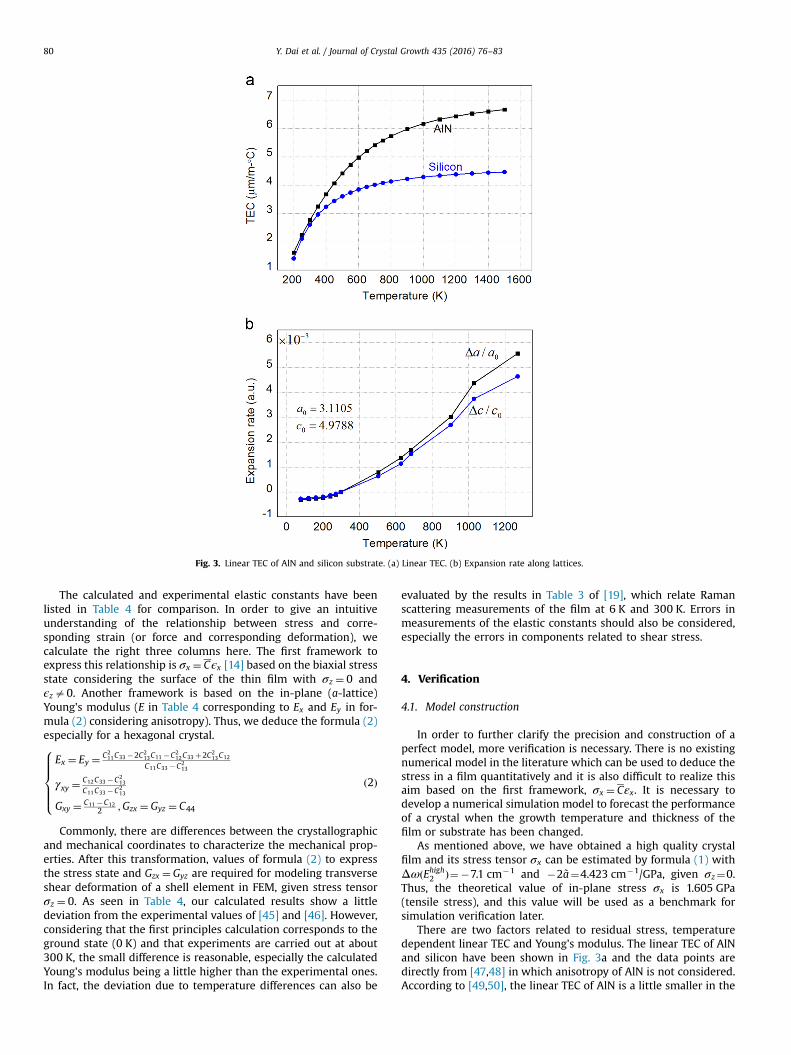
Fig. 3. Linear TEC of AlN and silicon substrate. (a) Linear TEC. (b) Expansion rate along lattices.
Y. Dai et al. / Journal of Crystal Growth 435 (2016) 76–8380
The calculated and experimental elastic constants have beenlisted in Table 4 for comparison. In order to give an intuitiveunderstanding of the relationship between stress and corre-sponding strain (or force and corresponding deformation), wecalculate the right three columns here. The first framework toexpress this relationship is σx ¼ Cϵx [14] based on the biaxial stressstate considering the surface of the thin film with σz ¼ 0 andϵza0. Another framework is based on the in-plane (a-lattice)Young's modulus (E in Table 4 corresponding to Ex and Ey in for-mula (2) considering anisotropy). Thus, we deduce the formula (2)especially for a hexagonal crystal.
Ex ¼ Ey ¼ C211C33 �2C2
13C11 �C212C33 þ2C2
13C12
C11C33 �C213
γxy ¼ C12C33 �C213
C11C33 �C213
Gxy ¼ C11 �C122 ;Gzx ¼ Gyz ¼ C44
8>>>><>>>>:
ð2Þ
Commonly, there are differences between the crystallographicand mechanical coordinates to characterize the mechanical prop-erties. After this transformation, values of formula (2) to expressthe stress state and Gzx ¼ Gyz are required for modeling transverseshear deformation of a shell element in FEM, given stress tensorσz ¼ 0. As seen in Table 4, our calculated results show a littledeviation from the experimental values of [45] and [46]. However,considering that the first principles calculation corresponds to theground state (0 K) and that experiments are carried out at about300 K, the small difference is reasonable, especially the calculatedYoung's modulus being a little higher than the experimental ones.In fact, the deviation due to temperature differences can also be
evaluated by the results in Table 3 of [19], which relate Ramanscattering measurements of the film at 6 K and 300 K. Errors inmeasurements of the elastic constants should also be considered,especially the errors in components related to shear stress.
4. Verification
4.1. Model construction
In order to further clarify the precision and construction of aperfect model, more verification is necessary. There is no existingnumerical model in the literature which can be used to deduce thestress in a film quantitatively and it is also difficult to realize thisaim based on the first framework, σx ¼ Cεx. It is necessary todevelop a numerical simulation model to forecast the performanceof a crystal when the growth temperature and thickness of thefilm or substrate has been changed.
As mentioned above, we have obtained a high quality crystalfilm and its stress tensor σx can be estimated by formula (1) withΔωðEhigh2 Þ¼�7.1 cm�1 and �2 ~a¼4.423 cm�1/GPa, given σz¼0.Thus, the theoretical value of in-plane stress σx is 1.605 GPa(tensile stress), and this value will be used as a benchmark forsimulation verification later.
There are two factors related to residual stress, temperaturedependent linear TEC and Young's modulus. The linear TEC of AlNand silicon have been shown in Fig. 3a and the data points aredirectly from [47,48] in which anisotropy of AlN is not considered.According to [49,50], the linear TEC of AlN is a little smaller in the
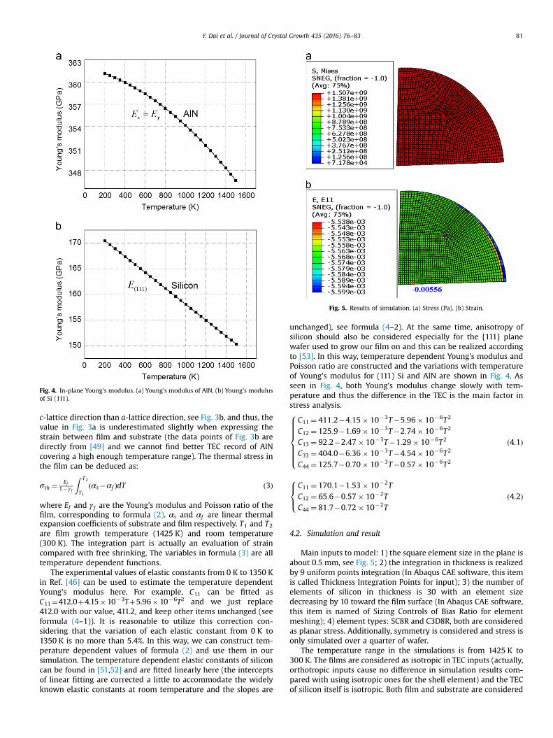
Fig. 4. In-plane Young's modulus. (a) Young's modulus of AlN. (b) Young's modulusof Si (111).
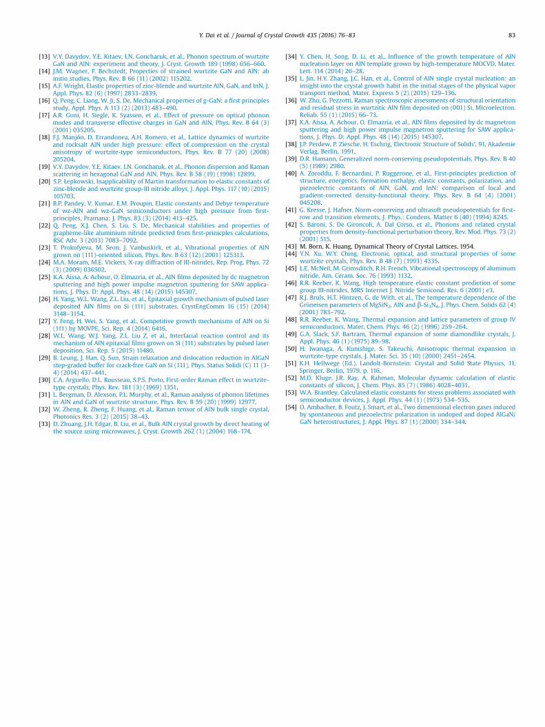
Fig. 5. Results of simulation. (a) Stress (Pa). (b) Strain.
Y. Dai et al. / Journal of Crystal Growth 435 (2016) 76–83 81
c-lattice direction than a-lattice direction, see Fig. 3b, and thus, thevalue in Fig. 3a is underestimated slightly when expressing thestrain between film and substrate (the data points of Fig. 3b aredirectly from [49] and we cannot find better TEC record of AlNcovering a high enough temperature range). The thermal stress inthe film can be deduced as:
σth ¼ Ef1� γf
Z T2
T1
ðαs�αf ÞdT ð3Þ
where Ef and γf are the Young's modulus and Poisson ratio of thefilm, corresponding to formula (2). αs and αf are linear thermalexpansion coefficients of substrate and film respectively. T1 and T2
are film growth temperature (1425 K) and room temperature(300 K). The integration part is actually an evaluation of straincompared with free shrinking. The variables in formula (3) are alltemperature dependent functions.
The experimental values of elastic constants from 0 K to 1350 Kin Ref. [46] can be used to estimate the temperature dependentYoung's modulus here. For example, C11 can be fitted asC11¼412.0þ4.15�10�3Tþ5.96�10�6T2 and we just replace412.0 with our value, 411.2, and keep other items unchanged (seeformula (4–1)). It is reasonable to utilize this correction con-sidering that the variation of each elastic constant from 0 K to1350 K is no more than 5.4%. In this way, we can construct tem-perature dependent values of formula (2) and use them in oursimulation. The temperature dependent elastic constants of siliconcan be found in [51,52] and are fitted linearly here (the interceptsof linear fitting are corrected a little to accommodate the widelyknown elastic constants at room temperature and the slopes are
unchanged), see formula (4–2). At the same time, anisotropy ofsilicon should also be considered especially for the {111} planewafer used to grow our film on and this can be realized accordingto [53]. In this way, temperature dependent Young's modulus andPoisson ratio are constructed and the variations with temperatureof Young's modulus for (111) Si and AlN are shown in Fig. 4. Asseen in Fig. 4, both Young's modulus change slowly with tem-perature and thus the difference in the TEC is the main factor instress analysis.
C11 ¼ 411:2�4:15� 10�3T�5:96� 10�6T2
C12 ¼ 125:9�1:69� 10�3T�2:74� 10�6T2
C13 ¼ 92:2�2:47� 10�3T�1:29� 10�6T2
C33 ¼ 404:0�6:36� 10�3T�4:54� 10�6T2
C44 ¼ 125:7�0:70� 10�3T�0:57� 10�6T2
8>>>>>><>>>>>>:
ð4:1Þ
C11 ¼ 170:1�1:53� 10�2T
C12 ¼ 65:6�0:57� 10�2TC44 ¼ 81:7�0:72� 10�2T
8><>: ð4:2Þ
4.2. Simulation and result
Main inputs to model: 1) the square element size in the plane isabout 0.5 mm, see Fig. 5; 2) the integration in thickness is realizedby 9 uniform points integration (In Abaqus CAE software, this itemis called Thickness Integration Points for input); 3) the number ofelements of silicon in thickness is 30 with an element sizedecreasing by 10 toward the film surface (In Abaqus CAE software,this item is named of Sizing Controls of Bias Ratio for elementmeshing); 4) element types: SC8R and C3D8R, both are consideredas planar stress. Additionally, symmetry is considered and stress isonly simulated over a quarter of wafer.
The temperature range in the simulations is from 1425 K to300 K. The films are considered as isotropic in TEC inputs (actually,orthotropic inputs cause no difference in simulation results com-pared with using isotropic ones for the shell element) and the TECof silicon itself is isotropic. Both film and substrate are considered

Table 5Film properties of AlN film grown on different substrates.
Ref. σx ¼ σyðGPaÞ εxð�10�3Þ εzð�10�3Þ PPEð�10�3C=m2Þ Sub-strate
[34] �0.095 �0.192 0.033 0.279 Sap-phire
[35] 0.158 0.319 �0.055 �0.463 SiC[36] 0.452 0.913 �0.157 �1.325 Si
(001)[25] 1.809 3.655 �0.628 �5.303 Si
(111)Pre-se-nt
1.605 3.242 �0.557 �4.704 Si(111)
Y. Dai et al. / Journal of Crystal Growth 435 (2016) 76–8382
to be in an in-plane stress state and thus the silicon is consideredas isotropic but using {111} plane parameters, such as Young'smodulus and Poisson ratio. The parameters for the shell elementhave been calculated with formula (2) and the model is con-structed to be compatible with the same coordinates to consideranisotropy (the units in simulation are Pa and μm).
As seen in Fig. 5a, the simulated stress value of 1.507 GPa isvery close to the one, 1.605 GPa, deduced from Raman experiment.Considering that the linear TEC of AlN in Fig. 3a is underestimatedslightly, this simulated stress can be used as a conservative esti-mate for film design. The relationship between stress and strain isdifferent from the absolute mechanical relationship due to thermalcoupling. Although the stress is tensile, the system bears com-pressive strain because of cooling shrinkage, as shown in Fig. 5b.These strain values are for crystal growth temperature and are notsuitable for piezoelectric analysis. However, the model can supplynon-linear predictions of strain variation from room temperatureto working temperature by simulating twice.
The simulated stress is 1.51 GPa, close to the analytic value1.605 GPa if the flaw of TEC is not considered. However, there islittle difference between strain components (including εx ¼ εy andεz) in simulation. The main difference between mechanical vari-ables is the in-plane Poisson ratio γxy, see formula (2). This vari-able's value is 0.319 at 300 K in [46] and 0.269 for our calculationresults. The reason for this is still unknown.
4.3. Piezoelectric analysis
According to [54], the piezoelectric tensor PPE has three inde-pendent components (C6V point group):
PPE ¼ e33εzþe31ðεxþεyÞ ð5Þ
where piezoelectric coefficients: e33¼1.46 C/m2 and e31¼�0.6 C/m2 [54]. At the same time, the in-plane strain can be analyzed withσx ¼ Cϵx in Table 4 with σx¼1.605 GPa ðϵx ¼ ϵyÞ and the straintensor in the z direction, εz, can be analyzed according to Hook'slaw (γzx¼0.1717 in Table 4)
ϵzϵx ¼ �γzx ð6Þ
Thus, we obtain the value of the piezoelectric tensorPPE¼�4.7�10�3 C/m2. In this way, we rebuild Table 2 for com-parison in Table 5. As seen in the table, the stress and strain in thefilms grown on sapphire and SiC are much lower than whengrown on a silicon substrate, especially for {111} plane siliconwafers. At the same time, our results are close to the similar waferresults in [25], which is mainly aimed for SAW (Surface AcousticWave) applications.
5. Summary
In summary, we prepared a high quality monocrystalline filmof AlN grown on a Si (111) substrate and then investigated theproperties of AlN, combining experiments and computationalsimulations for understanding and design of high quality singlecrystal films. We calculated the intrinsic frequencies of Ramanactive phonons and compared them with experimental data. Thecalculated results show good agreement with Raman frequenciesfrom a bulk single crystal as stress-free data. Then, we calibratedthe Phonon Deformation Potential coefficient which is importantfor Raman based stress measurements. At the same time, elasticconstants are also calculated and compared with experiments.Both of them are consistent with corresponding experimentalrecords.
We successfully develop a numerical model to verify the cal-culation above and the model itself is also useful to predictproperties of crystal films. We have carried out a simulation usingour model with temperature dependent data records of [46] asinput. The simulated stress is 1.51 GPa, which agree a well with theanalytic value 1.605 GPa. The deviations due to temperature dif-ferences are considered which relate Raman scattering measure-ments of the film at 6 K and 300 K. At last, the stress, strain, andpiezoelectric properties were analyzed and compared with filmson substrates of Sapphire, SiC, and Silicon with different surfaces.
Acknowledgment
The support of Basic Research (973) from Ministry of Scienceand Technology with Contract number of 2011CB309504 is highlyappreciated. Prof. Qian Sun is also grateful to the financial supportfrom the National Natural Science Foundation of China (Grant nos.61534007, 61404156, and 61522407), the National High Technol-ogy Research and Development Program of China (863 Program)(Grant no. 2013AA031901), Suzhou Science and Technology Pro-gram (Grant no. ZXG2013042), and the Recruitment Program ofGlobal Experts (1000 Youth Talents Plan). Authors are also gratefulto the Analytical and Testing Center, Huazhong University of Sci-ence and Technology for technical assistances.
References
[1] P. Motamedi, K. Cadien, Structural and optical characterization of low-temperature ALD crystalline AlN, J. Cryst. Growth 421 (2015) 45–52.
[2] I. Bryan, A. Rice, L. Hussey, et al., Strain relaxation by pitting in AlN thin filmsdeposited by metalorganic chemical vapor deposition, Appl. Phys. Lett. 102 (6)(2013) 061602.
[3] O. Ambacher, Growth and applications of group III-nitrides, J. Phys. D: Appl.Phys. 31 (20) (1998) 2653.
[4] S. Raghavan, J.M. Redwing, Group III-A Nitrides on Si: Stress and Micro-structural Evolution, CRC Press, Boca Raton, 2011.
[5] G. Dhanaraj, K. Byrappa, V. Prasad, et al., Springer Handbook of Crystal Growth,Springer Science & Business Media, 2010.
[6] S.A. Campbell, The Science and Engineering of Microelectronic Fabrication,second ed., Oxford University Press, New York, 1996.
[7] M. Kuball, Raman spectroscopy of GaN, AlGaN and AlN for process and growthmonitoring/control, Surf. Interface Anal. 31 (10) (2001) 987–999.
[8] G. Callsen, M.R. Wagner, J.S. Reparaz, et al., Phonon pressure coefficients anddeformation potentials of wurtzite AlN determined by uniaxial pressure-dependent Raman measurements, Phys. Rev. B 90 (20) (2014) 205206.
[9] A. Sarua, M. Kuball, J.E. Van Nostrand, Deformation potentials of the E2 (high)phonon mode of AlN, Appl. Phys. Lett. 81 (8) (2002) 1426–1428.
[10] J. Gleize, M.A. Renucci, J. Frandon, et al., Phonon deformation potentials ofwurtzite AlN, J. Appl. Phys. 93 (4) (2003) 2065–2068.
[11] T. Kallel, M. Dammak, J. Wang, et al., Raman characterization and stress ana-lysis of AlN: Er3þ epilayers grown on sapphire and silicon substrates, Mater.Sci. Eng.: B 187 (2014) 46–52.
[12] P. Giannozzi, S. De Gironcoli, P. Pavone, et al., Ab initio calculation of phonondispersions in semiconductors, Phys. Rev. B 43 (9) (1991) 7231.
Y. Dai et al. / Journal of Crystal Growth 435 (2016) 76–83 83
[13] V.Y. Davydov, Y.E. Kitaev, I.N. Goncharuk, et al., Phonon spectrum of wurtziteGaN and AlN: experiment and theory, J. Cryst. Growth 189 (1998) 656–660.
[14] J.M. Wagner, F. Bechstedt, Properties of strained wurtzite GaN and AlN: abinitio studies, Phys. Rev. B 66 (11) (2002) 115202.
[15] A.F. Wright, Elastic properties of zinc-blende and wurtzite AlN, GaN, and InN, J.Appl. Phys. 82 (6) (1997) 2833–2839.
[16] Q. Peng, C. Liang, W. Ji, S. De, Mechanical properties of g-GaN: a first principlesstudy, Appl. Phys. A 113 (2) (2013) 483–490.
[17] A.R. Goni, H. Siegle, K. Syassen, et al., Effect of pressure on optical phononmodes and transverse effective charges in GaN and AlN, Phys. Rev. B 64 (3)(2001) 035205.
[18] F.J. Manjón, D. Errandonea, A.H. Romero, et al., Lattice dynamics of wurtziteand rocksalt AlN under high pressure: effect of compression on the crystalanisotropy of wurtzite-type semiconductors, Phys. Rev. B 77 (20) (2008)205204.
[19] V.Y. Davydov, Y.E. Kitaev, I.N. Goncharuk, et al., Phonon dispersion and Ramanscattering in hexagonal GaN and AlN, Phys. Rev. B 58 (19) (1998) 12899.
[20] S.P. Łepkowski, Inapplicability of Martin transformation to elastic constants ofzinc-blende and wurtzite group-III nitride alloys, J. Appl. Phys. 117 (10) (2015)105703.
[21] B.P. Pandey, V. Kumar, E.M. Proupin, Elastic constants and Debye temperatureof wz-AlN and wz-GaN semiconductors under high pressure from first-principles, Pramana: J. Phys. 83 (3) (2014) 413–425.
[22] Q. Peng, X.J. Chen, S. Liu, S. De, Mechanical stabilities and properties ofgrapheme-like aluminium nitride predicted from first-prinicples calculations,RSC Adv. 3 (2013) 7083–7092.
[23] T. Prokofyeva, M. Seon, J. Vanbuskirk, et al., Vibrational properties of AlNgrown on (111)-oriented silicon, Phys. Rev. B 63 (12) (2001) 125313.
[24] M.A. Moram, M.E. Vickers, X-ray diffraction of III-nitrides, Rep. Prog. Phys. 72(3) (2009) 036502.
[25] K.A. Aissa, A. Achour, O. Elmazria, et al., AlN films deposited by dc magnetronsputtering and high power impulse magnetron sputtering for SAW applica-tions, J. Phys. D: Appl. Phys. 48 (14) (2015) 145307.
[26] H. Yang, W.L. Wang, Z.L. Liu, et al., Epitaxial growth mechanism of pulsed laserdeposited AlN films on Si (111) substrates, CrystEngComm 16 (15) (2014)3148–3154.
[27] Y. Feng, H. Wei, S. Yang, et al., Competitive growth mechanisms of AlN on Si(111) by MOVPE, Sci. Rep. 4 (2014) 6416.
[28] W.L. Wang, W.J. Yang, Z.L. Liu Z, et al., Interfacial reaction control and itsmechanism of AlN epitaxial films grown on Si (111) substrates by pulsed laserdeposition, Sci. Rep. 5 (2015) 11480.
[29] B. Leung, J. Han, Q. Sun, Strain relaxation and dislocation reduction in AlGaNstep-graded buffer for crack-free GaN on Si (111), Phys. Status Solidi (C) 11 (3-4) (2014) 437–441.
[30] C.A. Arguello, D.L. Rousseau, S.P.S. Porto, First-order Raman effect in wurtzite-type crystals, Phys. Rev. 181 (3) (1969) 1351.
[31] L. Bergman, D. Alexson, P.L. Murphy, et al., Raman analysis of phonon lifetimesin AlN and GaN of wurtzite structure, Phys. Rev. B 59 (20) (1999) 12977.
[32] W. Zheng, R. Zheng, F. Huang, et al., Raman tensor of AlN bulk single crystal,Photonics Res. 3 (2) (2015) 38–43.
[33] D. Zhuang, J.H. Edgar, B. Liu, et al., Bulk AlN crystal growth by direct heating ofthe source using microwaves, J. Cryst. Growth 262 (1) (2004) 168–174.
[34] Y. Chen, H. Song, D. Li, et al., Influence of the growth temperature of AlNnucleation layer on AlN template grown by high-temperature MOCVD, Mater.Lett. 114 (2014) 26–28.
[35] L. Jin, H.Y. Zhang, J.C. Han, et al., Control of AlN single crystal nucleation: aninsight into the crystal growth habit in the initial stages of the physical vaportransport method, Mater. Express 5 (2) (2015) 129–136.
[36] W. Zhu, G. Pezzotti, Raman spectroscopic assessments of structural orientationand residual stress in wurtzitic AlN film deposited on (001) Si, Microelectron.Reliab. 55 (1) (2015) 66–73.
[37] K.A. Aissa, A. Achour, O. Elmazria, et al., AlN films deposited by dc magnetronsputtering and high power impulse magnetron sputtering for SAW applica-tions, J. Phys. D: Appl. Phys. 48 (14) (2015) 145307.
[38] J.P. Perdew, P. Ziesche, H. Eschrig, Electronic Structure of Solids', 91, AkademieVerlag, Berlin, 1991.
[39] D.R. Hamann, Generalized norm-conserving pseudopotentials, Phys. Rev. B 40(5) (1989) 2980.
[40] A. Zoroddu, F. Bernardini, P. Ruggerone, et al., First-principles prediction ofstructure, energetics, formation enthalpy, elastic constants, polarization, andpiezoelectric constants of AlN, GaN, and InN: comparison of local andgradient-corrected density-functional theory, Phys. Rev. B 64 (4) (2001)045208.
[41] G. Kresse, J. Hafner, Norm-conserving and ultrasoft pseudopotentials for first-row and transition elements, J. Phys.: Condens. Matter 6 (40) (1994) 8245.
[42] S. Baroni, S. De Gironcoli, A. Dal Corso, et al., Phonons and related crystalproperties from density-functional perturbation theory, Rev. Mod. Phys. 73 (2)(2001) 515.
[43] M. Born, K. Huang, Dynamical Theory of Crystal Lattices, 1954.[44] Y.N. Xu, W.Y. Ching, Electronic, optical, and structural properties of some
wurtzite crystals, Phys. Rev. B 48 (7) (1993) 4335.[45] L.E. McNeil, M. Grimsditch, R.H. French, Vibrational spectroscopy of aluminum
nitride, Am. Ceram. Soc. 76 (1993) 1132.[46] R.R. Reeber, K. Wang, High temperature elastic constant prediction of some
group III-nitrides, MRS Internet J. Nitride Semicond. Res. 6 (2001) e3.[47] R.J. Bruls, H.T. Hintzen, G. de With, et al., The temperature dependence of the
Grüneisen parameters of MgSiN2, AlN and β-Si3N4, J. Phys. Chem. Solids 62 (4)(2001) 783–792.
[48] R.R. Reeber, K. Wang, Thermal expansion and lattice parameters of group IVsemiconductors, Mater. Chem. Phys. 46 (2) (1996) 259–264.
[49] G.A. Slack, S.F. Bartram, Thermal expansion of some diamondlike crystals, J.Appl. Phys. 46 (1) (1975) 89–98.
[50] H. Iwanaga, A. Kunishige, S. Takeuchi, Anisotropic thermal expansion inwurtzite-type crystals, J. Mater. Sci. 35 (10) (2000) 2451–2454.
[51] K.H. Hellwege (Ed.), Landolt-Bornstein: Crystal and Solid State Physics, 11,Springer, Berlin, 1979, p. 116.
[52] M.D. Kluge, J.R. Ray, A. Rahman, Molecular dynamic calculation of elasticconstants of silicon, J. Chem. Phys. 85 (7) (1986) 4028–4031.
[53] W.A. Brantley, Calculated elastic constants for stress problems associated withsemiconductor devices, J. Appl. Phys. 44 (1) (1973) 534–535.
[54] O. Ambacher, B. Foutz, J. Smart, et al., Two dimensional electron gases inducedby spontaneous and piezoelectric polarization in undoped and doped AlGaN/GaN heterostructures, J. Appl. Phys. 87 (1) (2000) 334–344.