January 2, 2014, At IISc Bangalore
93
Hiroshi Iwai Frontier Research Center Tokyo Institute of Technology Futur of Nano CMOS Technology Futur of Nano CMOS Technology January 2, 2014, At IISc Bangalore 1
Transcript of January 2, 2014, At IISc Bangalore

Hiroshi Iwai
Frontier Research CenterTokyo Institute of Technology
Futur of Nano CMOS TechnologyFutur of Nano CMOS Technology
January 2, 2014, At IISc Bangalore
1

1. Back ground for nano-CMOS
2

First Computer Eniac: made of huge number of vacuum tubes 1946Big size, huge power, short life time filament
Today's pocket PCmade of semiconductor
has much higher performance with
extremely low power consumption
dreamed of replacing vacuum tube with solid‐state device
3

1960: First MOSFET by D. Kahng and M. Atalla
Top View
Al Gate
Source
Drain
Si
Si
Al
SiO2
Si
Si/SiO2 Interface is extraordinarily good
4

1970,71: 1st generation of LSIs
DRAM Intel 1103 MPU Intel 4004
5

Most Recent SD Card
128GB (Bite) = 128G X 8bit= 1T(Tera)bit
1T = 1012 = 1Trillion
Brain Cell:10~100 BillionWorld Population:7 Billion
Stars in Galaxy:100 Billion
In 2012
6

2.4cm X 3.2cm X 0.21cm
Volume:1. 6cm³ Weight:2g
Voltage:2.7 - 3.6V
Old Vacuum Tube:5cm X 5cm X 10cm, 100g, 50W
128 GB = 1Tbit
What are volume, weight, power consumption for 1Tbit
7

Old Vacuum Tube:5cm X 5cm X 10cm
1Tbit = 10,000 X 10,000 X 10,000 bitVolume = (5cm X 10,000) X (5cm X 10,000)
X (10cm X 10,000)= 0.5km X 0.5km X 1km
500 m
1,000 m
1Tbit
Burji KhalifaDubai, UAE(Year 2010)
828 m
Indian TowerMumbai, India(Year 2016)
700 m
700 m
Pingan IntenationalFinance Center
Shanghai, China(Year 2016)
8

Old Vacuum Tube:50W
1Tbit = 1012bitPower = 0.05kWX1012=50 TW
Nuclear Power Generator1MkW=1BW We need 50,000 Nuclear Power Plant for
just one 128 GB memory
In Japan we have only 54 Nuclear Power Generator
Last summer Tokyo Electric Power Company (TEPCO) can
supply only 55BW.
We need 1000 TEPCO just one 128 GB memory
Imagine how many memories are used in the world! 9

So progress of integrated circuits is extremely
important for power saving
10

Brain: Integrated Circuits
Hands, Legs:Power device
Stomach:PV device
Ear, Eye:Sensor
Mouth:RF/Opto device
11

12
Near future smart-society has to treat huge data.
Demand to high-performance and low power CMOS become much more stronger.

13
Semiconductor Device Market will grow 5 times in 12 years, even
though, it is very matured market!!
Gartner: By K. Kim, CSTIC 2012
300B USD
2011
1,500B USD
2025

2. Current status of Si-CMOS device technologies
14

Downsizing
Thus, important forDecreasing cost, power
Increasing performance15
Decreasing sizeDecreasing capacitance

16
(1970) 10 μm 8 μm 6 μm 4 μm 3 μm 2 μm 1.2 μm
0.8 μm 0.5 μm 0.35 μm 0.25 μm 180 nm 130 nm
90 nm 65 nm 45 nm 32 nm (28 nm ) 22 nm(2012)
Feature Size / Technology Node
From 1970 to 2013 (Last year)
18 generationsLine width: 1/450
Area: 1/200,000
43 years 1 generation2.5 years
Line width: 1/1.43 = 0.70
Area: 1/2 = 0.5

What is the problem problem for downsizing?
Question
17

The problem for downsizing
Ioff increase: Transistor cannot be turned‐off.
Ioff (Off‐leakage current) between S and D
18
1. Punch‐through between S and D
2. Direct‐tunneling between S and D
3. Subthreshold current between S and D
S and D distance small
Ion & Ioff increase

19
1. Punch‐through between S and D

Gate oxide
Gate metal
Source Drain
1V0V0V
Substrate 0V DepletionRegion (DL)by Drain Bias
1V
0V 0V
tox and Vdd have to be decreased for better channel potential control IOFF Suppression
0V < Vdep<1V
0V
0V < Vdep<1VChannel
0V
0V
0V0V
0.5V
Large IOFF
Region governed By drain bias
Region governed by gate bias
tOX, Vdd thinning
DL touch with SRegion (DL)
Large IOFF
No tox. Vddthinning
Vdd
Vdd
20
Problem for downsizing
(Electron current)

21
1. Punch‐through between S and D
There are solutions to suppress the depletion layer
1.Decrease supply voltage Very difficult
2.Decrease tox to enhance the channel potential controllability by gate bias
as explained later
3. Gate/channel configuration change to enhance the channel potential controllability by gate bias
Fin‐FET, ET‐SOI, etc.

22
Decrease tox
Increase the Electric field between Gate &Channel
Increase the channel potential controllability by gate bias.
Suppress the depletion layer
Keep channel potential 0V

LLgate gate and tand toxox(EOT) scaling trend(EOT) scaling trendA. Toriumi (Tokyo Univ), IEDM 2006, Short Course
t ox(
(
23

24
Configuration change for channel and gate structures for better control of channel potential.
Fin‐FET, ET‐SOI, etc.

1V0V
0V
S
0V
0V <V<1V
1V0V
0V
0V
0VS D
G
G
G
Extremely Thin (or Fully-Depleted) SOI
Planar ET (or FD) SOI25
Si
SiO2
Extremely thin Si
Drain bias induced depletion
- Make Si layer thin- Control channel potential also from the bottom

1V0V
0V
S
0V
0V <V<1V
1V0V
0V
0V
0VS D
G
G
G
Surrounding gate structure (Multiple gates)
Planar Multi gate26
Si fin or nanowire
Drain bias induced depletion
- Make Si layer thin- Control channel potential also by multiple gates
not only from top & bottom but maybe also from side

Fin Tri-gate(Variation)
Ω-gate All-around
G G G
G
GNanowire structures in a wide meaning
27
G
Tri-gate

Our work at TIT: Our work at TIT: ΩΩ--gate Si Nanowiregate Si NanowireS. Sato et al., pp.361, ESSDERC2010 (Tokyo Tech.)
19 nm
12 nm
1.E-12
1.E-11
1.E-10
1.E-09
1.E-08
1.E-07
1.E-06
1.E-05
1.E-04
1.E-03
-1.5 -1.0 -0.5 0.0 0.5 1.010-12
Gate Voltage (V)
pFET nFET
10-11
10-10
10-9
10-8
10-7
10-6
10-5
10-4
10-3
Dra
in C
urre
nt (A
)
Vd=-50mV
Vd=-1V
Vd=50mV
Vd=1V
1.E-12
1.E-11
1.E-10
1.E-09
1.E-08
1.E-07
1.E-06
1.E-05
1.E-04
1.E-03
-1.5 -1.0 -0.5 0.0 0.5 1.010-12
Gate Voltage (V)
pFET nFET
10-11
10-10
10-9
10-8
10-7
10-6
10-5
10-4
10-3
Dra
in C
urre
nt (A
)
Vd=-50mV
Vd=-1V
Vd=50mV
Vd=1V
0 0.5 1 1.5 2ION (mA/µm)
Lg=65nm
0 0.5 1 1.5 2ION (mA/µm)
Lg=65nm
Lg=65nm
Poly-Si
SiO2
SiNSiN
SiO2
NW
・Conventional CMOS process
・High drive current
(1.32 mA/µm @ IOFF=117 nA/µm)
・DIBL of 62mV/V and SS of 70mV/dec for nFET 28

29
2. Direct‐tunneling between S and D
Wave function of electron penetrates the gate oxide potential barriers by quantum mechanical physics, when the gate oxide physical thickness is around 3 nm.

Tunnelingdistance
3 nm
Source DrainChannel
30
Ene
rgy
or P
oten
tial
for E
lect
ron
Direct‐tunnelcurrent
There is no solutions!
Downsizing limit is @ Lg = 3 nm.

31
3. Subthreshold current between S and D

32
Vg
Id
Vth (Threshold Voltage)
Vg=0V
SubthreshouldLeakage Current
Subtheshold leakage current of MOSFET
ONOFF
Ion
Subthresholdregion

33
Vg (V)1
0.3 V
0.5 V 1.0 V
Ion
Ioff
Id (A/µm)
10-7
10-5
10-11
10-9
Vd
Vth
0.15 V
0 0.5
Subthreshold leakage current
Electron EnergyBoltzmann statics
Exp (qV/kT)
Lg 1/2
Vd, Vg 1/2Vth 1/2
Ioff 103 in this exampleHowever
Because of log-linear dependence

34
Vg
Id
Vth (Threshold Voltage)
Vg=0V
SubthreshouldLeakage Current
Subtheshold leakage current of MOSFET
Subthreshold CurrentIs OK at Single Tr. level
But not OKFor Billions of Trs.
ONOFF
Ion
Subthresholdregion

35
3. Subthreshold current between S and D
Solution: however very difficult
Keep Vth as high as possible‐ Do not decrease supply voltage, Vd
‐ Suppress variability in VthHowever, punchthough enhanced
Thus, subthreshold current will limit the downsizing, especially for mobile devices

36Subthreshold Leakage (A/µm)
Ope
ratio
n Fr
eque
ncy
(a.u
.)
e)
100
10
1
Source: 2007 ITRS Winter Public Conf.
The limit is deferent depending on application

How far can we go for production?
10µm 8µm 6µm 4µm 3µm 2µm 1.2µm 0.8µm 0.5µm
0.35µm 0.25µm 180nm 130nm 90nm 65nm 45nm 32nm
(28nm) 22nm 14nm 11.5 nm 8nm 5.5nm? 4nm? 2.9 nm?
Past 0.7 times per 2.5 years
Now Future
・At least 4,5 generations to 8 ~ 5 nm
37
Intermediatenode
Direct-tunnelSubthresholdpunchthrough
Limit depending on applications
Fundamentallimit

However, careful about the name of technology!
22 nm Technology by Intel
Lg (Gate length) = 30 nm (HP), 34 nm (MP), 34 nm or larger (SP)
IEDM 2012, VLSI 2013
10 nm Technology by Leti (FD-SOI)
Lg (Gate length) = 15 nm
ECS 2013
Recently, Gate length (Lg) is much larger than the Technology name

The rate for the shrinkage for the gate length and line pitch will be larger than 0.7 in near future, because of the subthreshold leakage, and also because of the delay in EUV lithography.
As a result, we will have more technology generations until reaching the downsizing limit,and the time to reach the limit will be delayed.

HP MP SP
TOX,E (nm) 0.9 0.9 0.9
LGATE (nm) 30 34 34
IOFF (nA/um) 20-100 5-20 1-5
Tri-gate has been implemented since 22nm node, enabling further scaling
C. Auth et al., pp.131, VLSI2012 (Intel)
TriTri--gate implementation for transistors gate implementation for transistors
40

How far can we go for production?
41
Thus, we may go down to “5 nm”technology by choozing whatever gate length we want for the application.

More Moore to More More MooreMore Moore to More More Moore
65nm 45nm 32nm
Technology node
M. Bohr, pp.1, IEDM2011 (Intel)P. Packan, pp.659, IEDM2009 (Intel)C. Auth et al., pp.131, VLSI2012 (Intel)T. B. Hook, pp.115, IEDM2011 (IBM)S. Bangsaruntip et al., pp.297, IEDM2009 (IBM)
Lg 35nm Lg 30nm
(Fin,Tri, Nanowire)
22nm 15nm, 11nm, 8nm, 5nm, 3nm
Alternative (III-V/Ge) Channel FinFET
Emerging Devices
Tri-Gate
Now Future
Si channelSi
Others
(ETSOI)Planar
Si is still main stream for future !! ET: Extremely Thin28nm

HighHigh--k gate dielectricsk gate dielectrics
Continued research and development
SiO2 IL (Interfacial Layer) is used at Si interface to realize good mobility
Technology for direct contact of high-k and Si is necessary
Remote SiO2-IL scavengingHfO2 (IBM)
EOT=0.52 nm
Si
La-silicate
MG
Direct contact with La-silicate (Tokyo.Tech)
T. Ando, et al., p.423, IEDM2009, (IBM) T. Kawanago, et al., T-ED, vol. 59, no. 2, p. 269, 2012 (Tokyo Tech.)
K. Mistry, et al., p.247, IEDM 2007, (Intel)
TiN
HfO2
Si
SiO2
EOT=0.9nmHfO2/SiO2(IBM)
T.C. Chen, et al., p.8, VLSI 2009, (IBM)
Hf-based oxides
45nmEOT:1nm
32nmEOT:0.95nm
22nmEOT:0.9nm
15nm, 11nm, 8nm, 5nm, 3nm,
K. Kakushima, et al., p.8, IWDTF 2008, (Tokyo Tech.)
EOT=0.37nm EOT=0.40nm EOT=0.48nm
0.48 → 0.37nm Increase of Id at 30%43

How far can we go for production?
44
Now, Ion/Ioff ratio is typically 106.
However, it degrades significantly with decrease in Vsupply.
Rather than Ioff value, Ion/Ioff ratio is important.

[a] C. Auth et al., pp.131, VLSI2012 (Intel).[b] K. Mistry et al., pp.247, IEDM2007 (Intel).[c] H.-J. Cho et al., pp.350, IEDM2011 (Samsung).[d] S. Saitoh et al., pp.11, VLSI2012 (Toshiba).[e] S. Bangsaruntip et al., pp.297, IEDM2009 (IBM).
[f] T. Yamashita et al., pp.14, VLSI2011 (IBM).[g] A. Khakifirooz et al., pp.117, VLSI2012 (IBM).
IIONON and Iand IOFFOFF benchmarkbenchmark
[h] G. Bidal et al., pp.240, VLSI2009 (STMicroelectronics).[i] S. Sato et al., pp.361, ESSDERC2010 (Tokyo Tech.)[j] K. Cheng et al., pp.419, IEDM2012 (IBM)
1
10
100
1000
10000
0.6 0.8 1 1.2 1.4 1.6 1.8 2 2.2ION [mA/µm]
I OFF
[nA
/µm
]NMOS
Intel [a]Bulk 32nmVDD=0.8V
Intel [a]Tri-Gate 22nmVDD=0.8V
Intel [b]Bulk 45nmVDD=1V
Toshiba [d]Tri-Gate NWVDD=1V
Samsung [c]Bulk 20nmVDD=0.9V
IBM [5]GAA NWVDD=1V
IBM [g]FinFET 25nmVDD=1V
IBM [g]ETSOIVDD=0.9V
IBM [g]ETSOIVDD=1V
STMicro. [h]GAA NWVDD=0.9V
STMicro. [h]GAA NWVDD=1.1V
Tokyo Tech. [i]Ω-gate NWVDD=1V
IBM [j]ETSOIVDD=0.9VIeff
1
10
100
1000
10000
0.6 0.7 0.8 0.9 1 1.1 1.2 1.3 1.4 1.5 1.6ION [mA/µm]
I OFF
[nA
/µm
]
PMOSIntel [a]Bulk 32nmVDD=0.8V
Intel [a]Tri-Gate 22nmVDD=0.8V
Intel [b]Bulk 45nmVDD=1V
IBM [g]ETSOIVDD=1VSamsung [c]
Bulk 20nmVDD=0.9V
IBM [e]GAA NWVDD=1V
IBM [f]FinFET 25nmVDD=1V
IBM [g]ETSOIVDD=0.9V
STMicro. [h]GAA NWVDD=1.1V
IBM [j]ETSOIVDD=0.9VIeff

Nanowire/Tri gate MOSFETs have advantage not only suppressing Ioff, but also for increasing Ion over planer MOSFETs
46
1. Because of higher mobility due to lower vertical electric field
2. Because of higher carrier density at the round corner

47
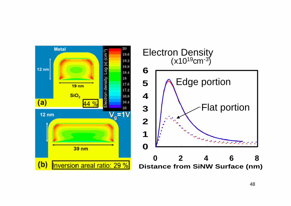
0 .E + 0 0
1 .E + 1 9
2 .E + 1 9
3 .E + 1 9
4 .E + 1 9
5 .E + 1 9
6 .E + 1 9
0 2 4 6 8Distance from SiNW Surface (nm)
6543210
角の部分
平らな部分
電子濃度(x1019cm-3)Electron Density
Edge portion
Flat portion
48

3. Problems
49
We have to decrease Si layer thickness to better control of channel potential by gate bias.
Significant decrease in conduction or Ion.

ShortShort--channel effectchannel effectT. Skotnicki, IEDM 2009 Short Course (STMicroelectronics)
50

DrainDrain--induced barrier loweringinduced barrier loweringT. Skotnicki, IEDM 2010 Short Course (STMicroelectronics)
51

SubSub--threshold Slopethreshold SlopeT. Skotnicki, IEDM 2010 Short Course (STMicroelectronics)
110 mV/dec
85 mV/dec
75 mV/dec
65 mV/dec
95 mV/dec
52

3. Problems
53
Mobility degradation.

S. Bangsaruntip et al., pp.297, IEDM2009 (IBM), K. Tachi et al., pp.313, IEDM2009 (CEA-LETI)
Decreasing the diameter of NW
Problems in MultiProblems in Multi--gategate
Improvedshort-channel control
Severe mobility degradation
Significant µ degradationat diameter < 10 nm
Need to decrease diameter for SCH
54

K. Uchida et al., pp.47, IEDM2002 (Toshiba)
Problems in SOIProblems in SOI
Mobility is also decreased with decreasing the Si thickness of SOI transistor similar to the NW transistor. 55
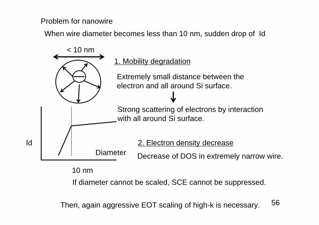
When wire diameter becomes less than 10 nm, sudden drop of IdProblem for nanowire
IdDiameter
10 nm
2. Electron density decrease
If diameter cannot be scaled, SCE cannot be suppressed.
Then, again aggressive EOT scaling of high-k is necessary. 56
< 10 nm1. Mobility degradation
Extremely small distance between the electron and all around Si surface.
Strong scattering of electrons by interaction with all around Si surface.
Decrease of DOS in extremely narrow wire.

3. Problems
57
Carrier density degradation.

Number of quantum channels
Energy band of Bulk Si
Eg
By Prof. Shiraishi of Tsukuba univ.
Energy band of 3 x 3 Si wire
4 channels can be used
Eg
58

59By Profs. Oshiyama and Iwata, U. of Tokyo
Diameter dependence

By Profs. Oshiyama and Iwata, U. of Tokyo
Wire cross section dependence.
What cross section gives best solution forSCE suppression and drive current?.
60

J. B. Chang et al., pp.12, VLSI2012 (IBM)
VVthth variabilityvariability
nFETs pFETs
Significant increase in Vth variability with decreasing Fin width
61

K. Kim, pp.1, IEDM2010 (Samsung)1.21.1
1
0.9
0.8
0.7
0.6
0.5
EO
T [n
m]
202020152010Year
12
10
8
6
4
2
0
Body Thickness [nm
]
Multi-Gate
Planar
ITRS2011
Fin width
Trend 1
Trend 2
Trend 3 ?
EOT Scaling TrendsEOT Scaling Trends
Smaller wire/fin width is necessary for SCE suppression
But mobility and ION severely degrade with wire/fin width reduction
Therefore even in multi-gate structures, EOT scaling should be accelerated to provide SCE immunity 62

High-k beyond 0.5 nm
63

Limit in tLimit in toxox thinningthinning
R.Chau, et al., (Intel) IWGI 2003
64
Gate oxide should be thicker than mono atomic layer
0.8 nm gate oxide thickness MOSFETs operate0.8 nm Distance of 3 Si atoms 2 mono layers

Limit in tLimit in toxox thinningthinningR.Chau, et al., (Intel) IWGI 2003
1 0.010.1
1
10
100
1000
0.1
0.01
0.001
Pow
er D
ensi
ty [W
/cm
2 ]
Gate Length [µm]
Active Power
Passive PowerGate
Leakage
Gate Leakage Power Density becomes significantly large with Lg reduction, and thus, with tox thinning!!
W.F.Clark, (IBM) VLSI 2007 Short Course
65

To use high-k dielectrics
Thin SiO2
Thick high-k dielectrics
Almost the same electric characteristics
However, very difficult and big challenge!
K: Dielectric Constant
5 times thicker
Small leakageCurrent
K=4K=20
SolutionSolution
SiO2 High-k
66

Equivalent Oxide Thickness (EOT)Equivalent Oxide Thickness (EOT)
Silicon Substrate
S D
Silicon Substrate
S D
SiO2
Poly-Si
C Poly
COX
CSi
High-kCOX
CSi
Equivalent Oxide Thickness (EOT): gate dielectrics itself, Cox
Capacitance Equivalent Thickness (CET): entire gate stack,
Metal gate can eliminate the poly-Si depletion.
Inversion CET = Tinv ≈ EOT + 0.4nm with metal gate electrode
Metal
Cmetal
Poly-Si(1020cm-3)
K. Natori, et al., (Tsukuba Univ) SSDM 2005, p.286
CMetal(EOT: 0.1 nm)
Depletion
Cmetal is finite because of quantum effect. In other words electron is not a point charge
located at the interface but distributed charge.
(EOT: 0.3 nm)
Combination of high-k and metal gate is important
67

R. Hauser, IEDM Short Course, 1999Hubbard and Schlom, J Mater Res 11 2757 (1996)
Gas or liquidat 1000 K
H
Radio activeHe
Li BeB C N O F Ne
① Na Mg Al Si P S Cl Ar
② ① ① ① ① ① ① ① ① ① ① K Ca Sc Ti V Cr Mn Fc Co Ni Cu Zn Ga Ge As Se Br Kr ① ① ① ① ① ① ① ① ① ① Rh Sr Y Zr Nb Mo Tc Ru Rb Pd Ag Cd In Sn Sb Te I Xe ③ ① ① ① ① ① ① ① Cs Ba
HfTa W Re Os Ir Pt Au Hg Tl Pb Bi Po At Rn
Fr Ra Rf Ha Sg Ns Hs Mt
La Ce Pr Nd Pm Sm Eu Gd Tb Dy Ho Er TmYb Lu Ac Th Pa U Np Pu Am Cm Bk Cf Es Fm Md No Lr
Candidates
Na Al Si P S Cl Ar
② ① ① ① ① ① ① ① ① ① K Sc Ti V Cr Mn Fc Co Ni Cu Zn Ga Ge As Se Br Kr ① ① ① ① ① ① ①
Ac Th Pa U Np Pu Am Cm Bk Cf Es Fm Md No Lr
②
③
Unstable at Si interfaceSi + MOX M + SiO2①
Si + MOX MSiX + SiO2
Si + MOX M + MSiXOY
Choice of High-k elements for oxide
HfO2 based dielectrics are selected as the
first generation materials, because of
their merit in1) band-offset,
2) dielectric constant3) thermal stability
La2O3 based dielectrics are
thought to be the next generation materials, which may not need a
thicker interfacial layer
68

0 10 20 30 40 50Dielectric Constant
4
2
0
-2
-4
-6
SiO2
Ban
d D
isco
ntin
uity
[eV]
Si
XPS measurement by Prof. T. Hattori, INFOS 2003
Conduction band offset vs. Dielectric Constant
Band offset
Oxide
Leakage Current by Tunneling
69

SiO2-ILHfSix (k~4)
VO
IO
IOVO
VO
IOIO
VOHfO2
Si substrate SiO2-IL(k~4)
LaSix
VO
IOVO
IO
VO
IOLa2O3silicate
La-rich Si-rich
Si substrate
High PO2Low PO2 High PO2Low PO2
HfO2 case La2O3 case
Direct contact can be achieved with La2O3 by forming silicate at interfaceControl of oxygen partial pressure is the key for processing.
Our approach
K. Kakushima, et al., VLSI2010, p.69
Direct high-k/Si by silicate reaction

SiO2-ILHfSix (k~4)
VO
IO
IOVO
VO
IOIO
VOHfO2
Si substrate SiO2-IL(k~4)
LaSix
VO
IOVO
IO
VO
IOLa2O3silicate
La-rich Si-rich
Si substrate
High PO2Low PO2 High PO2Low PO2
SiO2 IL formation
Si substrate
silicate formation
Si substrate
HfO2 case La2O3 case
Direct contact can be achieved with La2O3 by forming silicate at interfaceControl of oxygen partial pressusre is the key for processing.
Our approach
K. Kakushima, et al., VLSI2010, p.69
Direct high-k/Si by silicate reaction

1837184018431846Binding energy (eV)
Inte
nsity
(a.u
)
Si sub.
Hf SilicateSiO2
500 oC
1837184018431846Binding energy (eV)
Inte
nsity
(a.u
)
Si sub.
Hf SilicateSiO2
500 oC
SiOx-IL
HfO2
W
1 nm
k=4
k=16
SiOx-IL growth at HfO2/Si Interface
HfO2 + Si + O2→ HfO2 + Si + 2O*→HfO2+SiO2
Phase separator
SiOx-IL is formed after annealingOxygen control is required for optimizing the reaction
Oxygen supplied from W gate electrode
XPS Si1s spectrum
D.J.Lichtenwalner, Tans. ECS 11, 319
TEM image500 oC 30min
H. Shimizu, JJAP, 44, pp. 6131

La-Silicate Reaction at La2O3/Si
La2O3
La-silicate
W
500 oC, 30 min
1 nm
k=8~14
k=23
1837184018431846Binding energy (eV)
Inte
nsity
(a.u
)
as depo.
300 oC
La-silicate
Si sub.
500 oC
1837184018431846Binding energy (eV)
Inte
nsity
(a.u
)
as depo.
300 oC
La-silicate
Si sub.
500 oC
La2O3 + Si + nO2→ La2SiO5, La2Si2O7,
La9.33Si6O26, La10(SiO4)6O3, etc.La2O3 can achieve direct contact of high-k/Si
XPS Si1s spectra TEM image
Direct contact high-k/Si is possible

5m
Robot
Flash Lamp
ALDRTAEntrance
Sputterfor MG
EB Deposition for HK5m
Cluster tool for HKMG Stack
74

Cluster Chambers for HKMG Gate Stack
Flash Lamp Anneal
EB Deposition: HK Sputter: MG
ALD: HK
Robot
RTA
Entrance
75

76
Shutter movement
Chip
Si Si SiSi
Metal Metal Metal Metal
Thin Thick
high-k
15cm
0.0E+00
5.0E-04
1.0E-03
1.5E-03
2.0E-03
2.5E-03
3.0E-03
3.5E-03
0 0.2 0.4 0.6 0.8 1
Vg=0VVg=0.2VVg=0.4VVg=0.6VVg=0.8VVg=1.0VVg=1.2V
0 0.2 0.4 0.6 0.8 1
Vg=0VVg=0.2VVg=0.4VVg=0.6VVg=0.8VVg=1.0VVg=1.2V
0 0.2 0.4 0.6 0.8 1
Vg=0VVg=0.2VVg=0.4VVg=0.6VVg=0.8VVg=1.0VVg=1.2VI d
(V)
Vth=-0.04VVth=-0.05VVth=-0.06V

Substrate
Moving Mask
SourceElectron Beam
Flux
Deposited thin film
77

78

79
L=0.5~100µm (8 kinds)W=10, 20, 50, 100µm(4 kinds)
30 different Trs
26 c
hips
1cm
1cm
1cm×1cm
p-Si
S Dn+ Sn+SiO2

1.E-05
1.E-04
1.E-03
1.E-02
1.E-01
1.E+00
1.E+01
0 0.5 1 1.5 2 2.5 3
EOT ( nm )
Cur
rent
den
sity
( A
/cm
2 )Al2O3HfAlO(N)HfO2HfSiO(N)HfTaOLa2O3Nd2O3Pr2O3PrSiOPrTiOSiON/SiNSm2O3SrTiO3Ta2O5TiO2ZrO2(N)ZrSiOZrAlO(N)
Gate Leakage vs EOT, (Vg=|1|V)
La2O3
HfO2
80

81
2
1.5
1
0.5
0
Cap
acita
nce
[µF/
cm2 ]
-1 -0.5 0 0.5 1Gate Voltage [V]
10kHz 100kHz 1MHz
20 x 20µm2 1.5
1
0.5
0
Cap
acita
nce
[µF/
cm2 ]
-1.5 -1 -0.5 0 0.5Gate Voltage [V]
20 x 20µm2
10kHz 100kHz 1MHz
2
1.5
1
0.5
0
Cap
acita
nce
[µF/
cm2 ]
-1.5 -1 -0.5 0 0.5Gate Voltage [V]
20 x 20µm2
10kHz 100kHz 1MHz
FGA500oC 30min FGA700oC 30min FGA800oC 30min
A fairly nice La-silicate/Si interface can be obtained with high temperature annealing. (800oC)
However, high-temperature anneal is necessary for the good interfacial property

substrate
①La gas feed
②Ar purge ③H2O feed
④Ar purge
Laligand H
O
substrate substrate substrate
1 cycle
La
C 3H7
3
L a
C 3H7
3
L a
C 3H7
3
CLaN
NH
C3H7
C3H7
La(iPrCp)3 La(FAMD)3
Precursor (ligand)
ALD is indispensable from the manufacturing viewpoint- precise control of film thickness and good uniformity
K. Ozawa, et al., (Tokyo Tech. and AIST) Ext. Abstr. the 16th Workshop on Gate Stack Technology and Physics., 2011, p.107.
82
ALD of La2O3

83
① silicate-reaction-formedfresh interface
metal
Si sub.
metal
Si sub.
La2O3 La-silicateSi Si
Fresh interface with silicate reaction
J. S. Jur, et al., Appl. Phys. Lett., Vol. 87, No. 10, (2007) p. 102908
② stress relaxation at interface by glass type structure of La
silicate.
La atomLa-O-Si bonding
Si sub.
SiO4tetrahedron network
FGA800oC is necessary to reduce the interfacial stress
S. D. Kosowsky, et al., Appl. Phys. Lett., Vol. 70, No. 23, (1997) pp. 3119
Physical mechanisms for small DitPhysical mechanisms for small Dit

0.4
0.6
0.8
1.0
1.2
1.4
1.6
1.8
2.0
600 700 800 900 1000As depo
~ ~
Annealing temperature (oC)
EOT
(nm
)
Annealed for 2 sLa2O3(3.5 nm)
W(60 nm)
TiN/W(12 nm)
TiN/W(6 nm)
TiN(45nm)/W(6nm)
00.5
11.5
22.5
33.5
44.5
-1 -0.5 0 0.5
Vg (V)
Cg
(uF/
cm2 )
Experiment
Cvc fittingTheory
EOT=0.55nm
TaN/(45nm)/W(3nm)900oC, 30min
EOT=0.55nm
84

-0.4
-0.3
-0.2
-0.1
0
0.1
0.2
0.5 0.55 0.6 0.65 0.7
Flat
-ban
d vo
ltage
(V)
EOT(nm)
TaN(45nm)/W(3nm)
900oC, 30min
Qfix=1×1011 cm-2
Fixed Charge density: 1×1011 cm-2
85

0 0.2 0.4 0.6 0.8 1.0
Drain Voltage (V)
0.2
0.4
0.6
0.8
1.0
Dra
in C
urre
nt (m
A)
Vg= 0.4V
Vg= 0.6V
Vg= 0.8V
Vg= 1.0V
Vg= 0.2V
Vg= 0 V
L/W = 5/20µm
T = 300K
Nsub = 3×1016cm-3
0
20
40
60
80
100
120
140
0 0.5 1 1.5 2 2.5
EOT = 0.40nm
L/W = 5/20µm
T = 300K
Nsub = 3×1016cm-3
Eeff [MV/cm]
Elec
tron
Mob
ility
[cm
2 /Vse
c]
EOT=0.40nm
Our Work at TIT: HighOur Work at TIT: High--k k
86
Our result at TIT

1.E-02
1.E-01
1.E+00
1.E+01
1.E+02
1.E+03
1.E+04
0.3 0.4 0.5 0.6 0.7 0.8
ITRS requirement
J gat
1 V
(A/c
m2 )
EOT (nm)
Benchmark of LaBenchmark of La--silicate dielectricssilicate dielectrics
T. Ando, et al., (IBM) IEDM 2009, p.423
0
50
100
150
200
250
300
0.3 0.4 0.5 0.6 0.7 0.8 0.9 1EOT (nm)
Mob
ility
(cm
2 /Vse
c)
at 1 MV/cm
Open square : Hf-based oxides
Solid circle: Our data
Our data: La-silicate gate oxide
La-silicate gate oxide
L.-Å. Ragnarsson, et al., (IMEC) Microelectron. Eng, vol. 88, no. 7, pp. 1317–1322, 2011.
87
Gate Leakage current Effective Mobility

Si-sub.
Metal
SiO2-IL
High-kSmall interfacial state
density at high-k/Si
Oxygen diffusion control for prevention of EOT increase
and oxygen vacancy formation in high-k
Thinning or removal of SiO2-IL for small EOT
Flat metal/high-k interface for better
mobility
O
Workfunction engineering for Vth control
Interface dipole control for Vth tuning
Suppression of oxygen vacancy
formation
Control of interface reaction and Si diffusion to high-k
Oxygen concentration control for prevention of EOT
increase and oxygen vacancy formation in high-k
Suppression of metal diffusion
Endurance for high temperature process
Remove contaminationintroduced by CVD
Reliability: PBTI, NBTI, TDDB
Suppression of gate leakage current
Suppression of FLP
88
Issues in high-k/metal gate stack

Si benchmark (nMOSFET)Si benchmark (nMOSFET)
89
EOT Mobility Vth SS DIBLGate stack Ref.
0.45nmTiN/Cap/HfO2 115cm2/Vs
(at 1x1013cm-2)IMEC
MEE20110.3V
(Lg=10um)
0.52nmTiN/Cap/HfO2 110cm2/Vs
(at 1x1013cm-2)IBM
VLSI2011~0.4V
(Lg=24nm) 90mV/dec 147mV/V
0.59nmMetal/HfO2 130cm2/Vs
(at 1MV/cm)0.45V
(Lg=1um) 75mV/decSematechVLSI2009
0.65nmMetal/Hf-basedSamsungVLSI2011
0.3~0.4V(Lg=~30nm) 90mV/dec 100mV/V
0.95nmMetal/Hf-basedIntel
IEDM2009~0.3V
(Lg=30nm) 100mV/dec ~200mV/V
0.62nmW/La-silicateTokyo Tech.T-ED2012
-0.08V(Lg=10um) ~70mV/dec
155cm2/Vs (at 1MV/cm)
0.55nmTiN/Cap/HfO2 140cm2/Vs
(at 1MV/cm)IBM
VLSI2009

90
Conclusions 1
Downsizing of MOSFETs is still important for high-speed low-power operation of logic LSIs.
Ioff will limit the downsizing.
Punchthrough component of Ioff will be suppressed by thinning tox and adopting new configuration such as FinFET or nanowire FET.
Direct tunneling will limit the downsizing @Lg = 3 nm.
Even before that, subthreshould leakage would limit the downsizing @ Lg > 3nm, depending on the application.

91
Conclusions 2
In the application, Ion/Ioff ratio is important.
The ratio is typically 106 for the present devices, however, it degrades significantly with decreasing the supply voltage.
Si nanowire FET has advantage not only on Ioff over planer FET, but also on Ion, because of better mobility and higher channel carrier density..
In order to suppress Ioff with decrease in Lg, the diameter of nanowire, width of fin, or thickness of Si film of SOI need to be shirked,
.However, with decreasing the above diameter, width or thickness less than several nano-meter, very significant decrease on Ion occurs, because of the degradation on mobility and carrier concenrtation.

92
Conclusions 3
If the diameter, width or thickness cannot be decreased, we need to decrease the EOT of high-k aggressively in order to suppress Ioff.
High-k EOT reduction trend is very slow – 0.05 nm for each generation --, for the moment.
The limit of EOT scaling is expected to be around 0.4 nm or so, considering the additional capacitances of channel and metal gate.
By changing the high-k material from HfO2 to La-silicate, we can obtain the good operation of MOSFET with EOT = 0.4 nm,
.Metal silicide Shottoky S/D will become important in order to suppress the S/D encroachment to the channel by dopant diffusion.

93
Conclusions 3
.
Downsizing of MOFET is becoming more and more important for low power high performance application in the future smart society, and will be accomplished in another 10 to 15 years, although the rate of the downsizing will become slow.
Thus, many challenging technology development will be necessary for another q0 to 15 years.
Thank you very much for your attention.