J. Asare, E. Türköz, B. Agyei-Tuffour, O. K. Oyewole, A. A ... deformation of wavy/buckle...
11
Effects of pre-buckling on the bending of organic electronic structures J. Asare, E. Türköz, B. Agyei-Tuffour, O. K. Oyewole, A. A. Fashina, J. Du, M. G. Zebaze Kana, and W. O. Soboyejo Citation: AIP Advances 7, 045204 (2017); doi: 10.1063/1.4975396 View online: http://dx.doi.org/10.1063/1.4975396 View Table of Contents: http://aip.scitation.org/toc/adv/7/4 Published by the American Institute of Physics
Transcript of J. Asare, E. Türköz, B. Agyei-Tuffour, O. K. Oyewole, A. A ... deformation of wavy/buckle...

Effects of pre-buckling on the bending of organic electronic structuresJ. Asare, E. Türköz, B. Agyei-Tuffour, O. K. Oyewole, A. A. Fashina, J. Du, M. G. Zebaze Kana, and W. O.Soboyejo
Citation: AIP Advances 7, 045204 (2017); doi: 10.1063/1.4975396View online: http://dx.doi.org/10.1063/1.4975396View Table of Contents: http://aip.scitation.org/toc/adv/7/4Published by the American Institute of Physics

AIP ADVANCES 7, 045204 (2017)
Effects of pre-buckling on the bending of organicelectronic structures
J. Asare,1,2 E. Turkoz,3 B. Agyei-Tuffour,4 O. K. Oyewole,1,2 A. A. Fashina,1,5
J. Du,3,6,7 M. G. Zebaze Kana,1,8 and W. O. Soboyejo6,9,a1Department of Theoretical and Applied Physics, African University of University of Scienceand Technology, Km 10 Airport Road, Abuja, Federal Capital Territory, Nigeria2Department of Physics, Faculty of Computing and Applied Sciences, Baze University,Plot 686 Cadastral Zone C00, Kuchigoro, Abuja, Federal Capital Territory, Nigeria3Department of Mechanical and Aerospace Engineering, Princeton University, 41 Olden Street,Princeton, New Jersey 08544, USA4Department of Materials Science and Engineering, African University of Scienceand Technology, Kilometer 10 Airport Road, Abuja, Federal Capital Territory, Nigeria5Department of Physical Sciences, Kampala International University, Kampala, Uganda6Department of Biomedical Engineering, Gateway Park Life Sciences and BioengineeringCenter, Worcester Polytechnic Institute, 60 Prescott Street, Worcester,Massachusetts 01605, USA7Department of Mechanical & Nuclear Engineering, Pennsylvania State University,University Park, Pennsylvania 16802, USA8Department of Materials Science and Engineering, Kwara State University, Malete,Kwara State, Nigeria9Department of Mechanical Engineering, Worcester Polytechnic Institute, 100 Institute Road,Worcester, Massachusetts 01609, USA
(Received 10 November 2016; accepted 20 January 2017; published online 6 April 2017)
This paper explores the extent to which pre-buckling of layers (in thin film mul-tilayered structures) can be used to increase the flexibility of organic electronicdevices. The deformation of wavy/buckle profiles, with a range of nano- andmicro-scale wavelengths, is modeled using finite element simulations. The pre-dictions from the models are then validated using experiments that involve thebending of layered structures that are relevant to flexible organic electronics. Theintroduction of pre-buckled profiles is shown to increase the range of deforma-tion that is applied to model structures, prior to onset of significant stresses andstrains. The implications of the work are discussed for the design of robust flex-ible organic solar cells. © 2017 Author(s). All article content, except where oth-erwise noted, is licensed under a Creative Commons Attribution (CC BY) license(http://creativecommons.org/licenses/by/4.0/). [http://dx.doi.org/10.1063/1.4975396]
I. INTRODUCTION
In recent years, there has been considerable interest in the development of low cost flexibleorganic solar cells with the potential to replace conventional silicon cells that are fabricated typicallyon glass substrates.1–3 However, the rigidity of the glass substrates limits the extent to which flexibleelectronics structures can be deformed without inducing cracks in the rigid and brittle glass substrates.4
There is, therefore, a need for approaches that can improve the deformation of flexible organic solarcells, without inducing cracks in the underlying substrates.5
Two approaches have been used in literature to improve the flexibility of organic solar cellsstructures.6–13 One involves the replacement of the glass substrates with bendable polymers, suchas polyethylene terephthalate (PET)14–19 or polydimethylsiloxane (PDMS),10,20–23 while the second
aCorrespondence to Professor Wole Soboyejo. Email: [email protected], Phone: +1-508-831-4694. Materials Program,Department of Mechanical Engineering, Worcester Polytechnic Institute, Worcester, MA 01605-2280, USA.
2158-3226/2017/7(4)/045204/10 7, 045204-1 © Author(s) 2017

045204-2 Asare et al. AIP Advances 7, 045204 (2017)
approach involves the introduction of pre-buckles that stretch and flatten out during deformation. Thepre-buckles also increase the range of deformation that can be applied to flexible organic electronicsprior to the onset of cracking and other stress/strain-induced failure mechanisms.24
Prior work on the deformation of flexible and stretchable organic electronics structures has beenreported by Bao et al.,4,25 Volinski et al.,26 Groenwold,27 Huang,28–30 Stafford et al.31 and Sariciftciand co-workers.6,32,33 Their work shows that pre-buckles with different wavelengths can improvethe flexibility of layered organic solar cell structures with different substrates. Similar reports ofimproved deformability have also been presented by Huang and co-workers,30,34–37 while Rogers etal.38 and Akogwu et al.20 have used pre-buckles to improve the “stretch-ability” of flexible organicelectronic structures.
Bao et al.4 have presented two methods that can be used to influence the elasticity of rigidmaterials. The first involves the dispersion of conductive materials in an elastic matrix (as exploitedby Wagner,39 Suo,40 Rogers,41 Sariciftci33), while the second involves the pre-buckling of elec-tronic structures deposited on elastomeric substrates. The latter have been investigated by Stafford,42
Sariciftci,43 Tarasovs and Andersons.44 The results show clearly that the potential application ofpre-buckled films (with controlled wavelengths and amplitudes) could have a significant effect onthe deformability and reliability of electronic devices.
Rogers et al.38 have also suggested that the buckle wavelength increases with increasing bucklefilm thickness. However, there have been only limited prior efforts to model the deformation offlexible organics cell structures under bending loads and deformation conditions45 that are relevantto flexible organic electronics.41
Furthermore, the flexibility of transparent electrodes has been achieved by structurally config-uring devices to accommodate most of the strain under mechanical deformation that minimizes thestrains in the conducting materials. These structural configurations have been classified into out-of-plane and in-plane structures.47–50 The most common out-of-plane structure is the ‘wavy’ structure,which is generally obtained by depositing conductive materials on pre-strained elastomeric substrates.When subsequently released, these conductive films spontaneously form periodic wavy structures inwhich most of the induced strains are absorbed by the structural changes.47 These have been likenedto accordion bellows, where increased buckling wavelengths and decreased buckling amplitudes canbe achieved.47,51,52
The fundamental advantage of the presented pre-buckled structure is its ability to permit largeelastic deformation protecting the active layers with limited strains. Thin films fabricated this wayare more compliant when compared to the bending strain which is less than that of pre-stretch.47–53
However, although the effects of pre-buckling have been studied,53 there is only a limited under-standing of pre-buckling on the deformation of flexible organic structures. Hence, this paper, therefore,presents the results of an experimental and computational study of the effects of this most commonout-of-plane structure (pre-buckling) on the deformation and failure of flexible organic solar cellstructures on polydimethylsiloxane (PDMS) substrates. The effects of pre-buckle wavelengths andamplitudes are modeled using finite element method. The stress/strain distributions and the defor-mation profiles associated with the bending of the pre-buckled profiles are computed for the modelflexible multilayer structures deposited experimentally. The increased deformation associated withthe flattening of the pre-buckles is determined for pre-buckles with different wavelengths and ampli-tudes. The implications of the results are then discussed for the design of flexible organic electronicstructures.54,55
II. EXPERIMENTAL PROCEDURE
This section utilizes un-stretched, pre-stretched and post-stretched structures in a study of thebending of model organic semiconductor layers on flexible PDMS substrates. It is important tonote that the un-stretched condition corresponds to the un-stretched PDMS substrate, while thepre-stretched condition corresponds to the stretched condition prior to the deposition of poly 3,4-ethylenedioxythiophene polystyrene sulfonate (PEDOT:PSS) thin film layer. The post-stretchedcondition corresponds to the subsequent deformation of the pre-buckled structure that is formed afterthe release of the PEDOT:PSS/PDMS structure.
045204-3 Asare et al. AIP Advances 7, 045204 (2017)
A. PDMS substrate preparation
The PDMS substrate was prepared from a Sylgard 184 elastomeric base and a silicone curingagent with 1:10 weight ratio, as described in our prior work.56 Observations show that increasing theweight ratio of the silicon curing agent makes the resulting PDMS less stretchable, as expected, sincesilicon acts as the cross-link (hardener) agent between the polymer chains.20 In any case, PDMSsubstrates with dimensions of 1.5mm and 4.5 cm × 1.25 cm were prepared by casting and curingthem in an aluminum mold.
B. PEDOT:PSS coating deposition
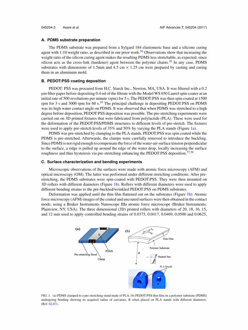
PEDOT: PSS was procured from H.C. Starck Inc., Newton, MA, USA. It was filtered with a 0.2µm filter paper before depositing 0.4 ml of the filtrate with the Model WS 650 Laurel spin-coater at aninitial rate of 500 revolutions per minute (rpm) for 5 s. The PEDOT:PSS was then spin coated at 1500rpm for 3 s and 3000 rpm for 60 s.18 The principal challenge in depositing PEDOT:PSS on PDMSwas its high water contact angle on PDMS. It was observed that when PDMS was stretched to a highdegree before deposition, PEDOT:PSS deposition was possible. The pre-stretching experiments werecarried out on 3D printed fixtures that were fabricated from polylactide (PLA). These were used forthe deformation of the PEDOT:PSS/PDMS structures to different levels of pre-stretch. The fixtureswere used to apply pre-stretch levels of 35% and 50% by varying the PLA stands (Figure 1a).
PDMS was pre-stretched by clamping to the PLA stands. PEDOT:PSS was spin coated while thePDMS is pre-stretched. Afterwards, the clamps were carefully removed to introduce the buckling.Since PDMS is not rigid enough to compensate the force of the water-air-surface tension perpendicularto the surface, a ridge is pulled up around the edge of the water drop, locally increasing the surfaceroughness and thus hysteresis via pre-stretching enhancing the PEDOT:PSS deposition.57,58
C. Surface characterization and bending experiments
Microscopic observations of the surfaces were made with atomic force microscopy (AFM) andoptical microscopy (OM). The latter was performed under different stretching conditions. After pre-stretching, the PDMS substrates were spin-coated with PEDOT:PSS. They were then mounted on3D rollers with different diameters (Figure 1b). Rollers with different diameters were used to applydifferent bending strains to the pre-buckled/wrinkled PEDOT:PSS on PDMS substrates.
Deformation was applied until the thin film flattened out on the substrates (Figure 1b). Atomicforce microscopy (AFM) images of the coated and uncoated surfaces were then obtained in the contactmode, using a Bruker Instruments Nanoscope IIIa atomic force microscope (Bruker Instruments,Plainview, NY, USA). The three dimensional (3D) printed rollers with diameters of 20, 18, 16, 15,and 12 mm used to apply controlled bending strains of 0.0375, 0.0417, 0.0469, 0.0500 and 0.0625,
FIG. 1. (a) PDMS clamped to a pre-stretching stand made of PLA. (b) PEDOT:PSS thin film on a polymer substrate (PDMS)undergoing bending showing its acquired radius of curvature, R when placed on PLA stands with different diameters.(Ref. 62,87).

045204-4 Asare et al. AIP Advances 7, 045204 (2017)
respectively. The axial strains were determined using the following expression:59–63
Strain=
(Thickness − of − PDMS
2
)Diametter − of − Roller
(1)
AFM was then used to characterize the wavelengths of the surfaces of the wrinkled/buckledPEDOT:PSS layers on PDMS. This was done after pre-stretching and bending to different strainlevels. AFM imaging was carried out in the contact mode using a Bruker Instruments Dimension3000 atomic force microscope (Bruker Instruments, Plainview, NY, USA).
III. MODELING
Finite element simulations where used to model the effects of bending on the pre-buckled films.The structures were modeled undergoing three-point bending, after introducing pre-buckled profileswith different wavelengths. Finite element modeling was carried out using the ABAQUS softwarepackage (ABAQUS CAE 6.12-1, Dassault Systemes, Pawtuckett, Rhode Island, USA). A 2D (twodimensional) plane stress model was built (Figures 2a and 2b).
The thickness of the PDMS was 1.5 mm in the model. This corresponded to the thickness ofthe PDMS substrate that was used in the experiments. It should be noted that the pre-buckles weresimulated using profiles of PEDOT:PSS that were in partial contact with the PDMS substrates priorto the application of bending (Figure 2a). The deformation of the pre-buckled structures then resultedin the flattening of the layers as the bending strains were increased (Figure 2b).
The mechanical properties of the individual layers (Young moduli and Poisson’s ratios) that wereused in the simulation are presented in Table I.63–66 Linear elastic deformation was also assumedin each of the layers. Structured quadrilateral meshes were used in the finite element model, alongwith standard bi-linear plane stress elements with incompatible modes. The two aluminum stoppersat both ends were fixed in the X, Y and Z directions (i.e. U1, U2 and U3, respectively). The middleroller was constrained to displace upward (i.e. move only in the U2 direction) upon the applicationof pressure.
The above procedure was repeated for the other layered structures in which the anode layer (ITO),the active layer (P3HT: PCBM), and the cathode (Aluminum) were pre-buckled and deformed on therelevant layers in model organic photovoltaic structures.16,18,19,67–71 The layer mechanical propertiesthat were used in the simulations are summarized in Table I.
FIG. 2. (a) Schematics of multilayer parts designed for the finite element analysis taking into consideration the experimentalparameters and (b) elemental view of buckle on PDMS.
TABLE I. Material Properties.
Materials Young’s Modulus, E/GPa Poisson’s ratio References
PDMS 0.003 0.48 64,86,87PEDOT: PSS 1.42 0.3 64Al 70 0.3 63

045204-5 Asare et al. AIP Advances 7, 045204 (2017)
IV. RESULTS AND DISCUSSION
A. Effects of pre-stretching on surface Topography
The AFM images revealed the presence of buckles, following release from small pre-stretchesof 18%, 25% and larger pre-stretches of 35% and 50% (Figure 3a–3d). These show clearly thatthe wavelengths of the resulting buckles decreased with increasing pre-stretch. Optical Microscopyimages of the surfaces of the PDMS and PEDOT:PSS/PDMS structures also revealed similar trendsin the pre- and post-stretched conditions (Figures 4a–4c)). These images also showed that the surfaceroughness (wavelengths) decrease with increasing pre-stretch.
Plots of the wavelengths of the buckled profiles (obtained from the contact mode AFM images)are presented in Figure 5. These were obtained for surfaces that were subjected to different levelsof pre-stretch. These show clearly that the wavelengths of the pre-buckled profiles decrease withincreasing pre-stretch. Similar results have been reported by Oyewole et. al.23 for the formation ofpre-buckles on the surfaces of pre-stretched and released Au films on PDMS substrates.
B. Effects of deformation on surface topography
In general, increased pre-stretch resulted in a reduction in the wavelengths of the pre-buckled pro-files (Figures 3 and 5). However, upon subsequent bending of the pre-buckled structures, the surfacesof the pre-buckled structures flattened out (Figures 6a and 6b). In the case of the samples producedafter 50% pre-stretch, the initial pre-buckled surfaces had wavelengths of about 0.13 microns. Thesurface wavelengths increased to 0.4545 microns, after applying a bending strain 0.0417. This isconsistent with a tendency to flatten out the buckles with increasing applied strain. In the case of thesamples that were subjected to a pre-stretch of 70%, the initial PEDOT:PSS/PDMS structures hadpre-buckles with a wavelength of about 16.7 nanometers. However, upon applying a bending strainof 0.0417, the surface to about 1.67 microns (See Table II).
C. Finite element simulations of three-point bending
The finite element simulations of the deformation of the pre-buckled PEDOT:PSS profiles on aPDMS substrate are presented in Figures 7a–7c. These show the progression of stress and deformationprofiles from the initial pre-buckled states to the conditions at which the buckles become flattened outdue to the application of tensile stresses through bending. The results clearly show that the stretchingof the surface layers flattens out the initially sinusoidal profiles.
The finite element predictions of the initial pre-buckle flattening conditions confirmed resultspresented in Table II, along with the experimental measurements of the forces per unit width requiredfor the flattening of the pre-buckles. These forces were observed to increase with decreasing pre-buckle wavelength. Hence, increased pre-stretch of the films, which gives rise to decreased pre-buckled wavelengths, is likely to increase the apparent film “deformability”.
FIG. 3. AFM images of micro-wrinkles observed with pre-stretched PDMS substrates after PEDOT:PSS deposition. (a): 18%pre-stretch. (b): 25% pre-stretch. (c): 35% pre-stretch. (d): 50% pre-stretch. [Note that the wavelength decreases in this order:(a) > (b) > (c) > (d)].

045204-6 Asare et al. AIP Advances 7, 045204 (2017)
FIG. 4. Optical Microscopic images of the surface topology of PDMS and PEDOT:PSS/PDMS structures; (a) is an opticalimage of un-stretched PDMS substrate; (b) 35% post-stretched PDMS substrate with PEDOT:PSS deposition, showing lesswrinkles, and (c) 50% post-stretched PDMS substrate with PEDOT:PSS deposition showing deep crack/trench images observedas surface features indicating more wrinkles.
Furthermore, the computed von Mises stress distributions obtained for the deformedpre-buckled films were used to characterize the deformation in multilayered structures(Al/P3HT:PCBM/PEDOT:PSS/ITO/PDMS and Al/P3HT:PCBM/PEDOT:PSS/PDMS) that are rele-vant to organic solar cells. The results are presented in Figures 8a and 8b. These show that the bendingof the films (for different initial pre-buckle wavelengths) results in increased von Mises stresses thatcan lead ultimately to the onset of plastic deformation in the Al cathode layers and the polymericlayers within the model organic solar cell structures.
Hence, the deformation that occurs, prior to flattening, is likely to extend the deforma-bility of the flexible multilayer structures, while the deformation that occurs, after the flat-tening can result in the build-up of stresses until the onset pf plasticity or fracture. Inter-facial failure can also occur between the layers, depending on the adhesion between thelayers.12,72,73
Finally, it is important to discuss the potential effects of transparent indium tin oxide (ITO) layersthat are often used as the anode of organic solar cells. Since these layers have relatively high moduli(Table I), they can result in higher stress distributions and elastic strain energies in flexible modelsolar cell structures (Figures 8a and 8b). These can lead ultimately to the cracking of the ITO layer,as observed in earlier work.17,70,74,75 There is, therefore, a need to avoid the use of ITO layers in thedevelopment of flexible organic solar cells.
FIG. 5. Buckling/wrinkling wavelengths changes as a function of pre-stretching percentage.

045204-7 Asare et al. AIP Advances 7, 045204 (2017)
FIG. 6. Schematics of an AFM tip measuring the wavelength of a substrate with wrinkles/buckles undergoing bending ondifferent PLA rollers; (a) Buckles exhibit small wavelengths due to less bending strains applied by courtesy of larger diameterPLA roller used, (b) Buckles flattened implying very high wavelength values due to large bending strain achieved on a smalldiameter PLA roller.
TABLE II. Pre-buckled wavelength before and after bending.
Pre-buckled Wavelength before Bending/µm Pre-buckled Wavelength after Bending/µm
0.1300 0.45450.0167 1.6700
D. Implications
The implications of the results are very significant. First, they show that pre-buckling can beused to increase the deformability of flexible organic solar cells (see Figures 8a and 8b), priorto the onset of failure by the plasticity or fracture of the film constituents. The improvements inflexibility can also be enhanced by the control of initial buckle wavelengths and amplitudes, whichcan be achieved by the use of pre-stretching methods (as done in the experimental section of thispaper).50,76
However, increased pre-buckle wavelengths can also result in higher film stresses that can inducefailure within the layers or between them. A balanced approach is, therefore, needed to deter-mine the pre-buckled configurations that improve flexibility/deformability, without compromisingthe conditions for final film failure.
Furthermore, from the literature,6,46,48,77,78 it is clear that further flexibility can be achievedby fabricating the devices on ultra-thin polymer substrates and laminating them unto a pre-strainedelastomers such as PDMS. The application of such ultra-thin substrates could decrease the bending
FIG. 7. Pre-buckled structure of PEDOT: PSS on PDMS with von Misses stress distribution at the onset of flattening forvarious wavelengths; (a) buckle with wavelength, λ0, at 15 N/mm2 pressure (b) buckle wavelength gradual increase on furtherapplication of bending moment to λ1 due to the stretching of the buckle at 37 N/mm2 pressure, and (c) complete flattening ofbuckle on PDMS substrate on applying 50 N/mm2 pressure.

045204-8 Asare et al. AIP Advances 7, 045204 (2017)
FIG. 8. Maximum strain and von Misses stresses in the different films for different amplitudes at constant wavelength witheffects of indium tin oxide layers in the pre-buckle structures; (a) strain energy variations and (b) stress distribution in thedifferent layers.
strains. However, the compliance of these structures would also be increased significantly. In anycase, the model PEDOT:PSS transparent electrode, explored in the current work is consistent withthe work of Drack et al.48 and Kim et al.77 who have produced flexible devices in which resistanceincreases to ∼30% after 10,000 cycles of stretching to strains of 50%.48,77
Furthermore, the current work suggests that improvements in the flexibility of pre-buckledorganic electronic structures can be estimated by considering the ratio of the strains to flatteningof a pre-buckled structure to the strain to failure of a non-pre-buckled structure. This means thatthe surface area of the device (if it is a solar cell) would have more wavy characteristics that couldimprove the harnessing of sunlight for photo-conversion to electricity.
The fabrication of the above organic solar cell structures could be achieved by the use of roll-to-roll printing16,79,80 and lamination processes.64,81 The optimization of such manufacturing processescould lead to the future scale up of emerging approaches for the design and fabrication of flexi-ble solar cells.82 The flexible organic solar cells could also be integrated into roofing tiles83 andelectronic textiles84–86 in which significant bending strains87 can be applied during fabrication andservice.
V. SUMMARY AND CONCLUDING REMARKS
This paper presents the results of an experimental and computational study of the deformationbehavior of pre-buckled thin films structures that are relevant to the deformation of flexible organicelectronics. The results show that the additional strain to flattening (of the pre buckles) enhances thedeformability/flexibility of the films. The strains to flattening also increase with increased pre-bucklewavelength. However, such increased pre-buckle amplitudes and wavelengths may also induce failureby film plasticity, fracture or delamination. A balanced approach is, therefore, needed for the designof robust pre-buckled layers for potential applications in flexible organic electronic structures.
ACKNOWLEDGMENTS
The authors are grateful to the World Bank STEP-B Program, the African Centers of ExcellenceProgram, the African Capacity Building Foundation, the African Development Bank, the Pan AfricanMaterials Institute (PAMI), the African University of Science and Technology (AUST), PrincetonUniversity, the Worcester Polytechnic Institute (WPI) and the Nelson Mandela Institution for theirfinancial support. Appreciation is also extended to scientist and technologists at the Physics AdvancedLaboratory at Sheda Science and Technology Complex, Abuja, Nigeria, and Princeton University,New Jersey, USA, for their assistance with experimental techniques.1 M.-C. Choi, Y. Kim, and C.-S. Ha, Prog. Polym. Sci. 33, 581 (2008).2 K. A. Arpin, A. Mihi, H. T. Johnson, A. J. Baca, J. A. Rogers, J. A. Lewis, and P. V Braun, Adv. Mater. 22, 1084 (2010).

045204-9 Asare et al. AIP Advances 7, 045204 (2017)
3 C. Battaglia, J. Escarre, K. Soderstrom, L. Erni, L. Ding, G. Bugnon, A. Billet, M. Boccard, L. Barraud, S. De Wolf,F.-J. Haug, M. Despeisse, and C. Ballif, Nano Lett. 11, 661 (2010).
4 D. J. Lipomi, B. C.-K. Tee, M. Vosgueritchian, and Z. Bao, Adv. Mater. 23, 1771 (2011).5 C. H. Hsueh and A. A. Wereszczak, J. Appl. Phys. 96, 3501 (2004).6 M. Kaltenbrunner, M. S. White, E. D. Głowacki, T. Sekitani, T. Someya, N. S. Sariciftci, and S. Bauer, Nat. Commun. 3, 1
(2012).7 Y. Zhang, Y. Huang, and J. A. Rogers, Curr. Opin. SOLID STATE Mater. Sci. ELSEVIER LTD. 10 (2015).8 M. Li, J. Xiao, J. Wu, R.-H. Kim, Z. Kang, Y. Huang, and J. A. Rogers, Acta Mech. Solida Sin. 23, 592 (2010).9 E.-H. Kil, K.-H. Choi, H.-J. Ha, S. Xu, J. A. Rogers, M. R. Kim, Y.-G. Lee, K. M. Kim, K. Y. Cho, and S.-Y. Lee, Adv.
Mater. 25, 1395 (2013).10 A. Blau, A. Murr, S. Wolff, E. Sernagor, P. Medini, G. Iurilli, C. Ziegler, and F. Benfenati, Biomaterials 32, 1778 (2011).11 Y. Zhang, H. Fu, Y. Su, S. Xu, H. Cheng, J. A. Fan, K.-C. Hwang, J. A. Rogers, and Y. Huang, Acta Mater. 61, 7816 (2013).12 D. Yu, O. K. Oyewole, D. Kwabi, T. Tong, V. C. Anye, J. Asare, E. Rwenyagila, A. Fashina, O. Akogwu, J. Du, and W.
O. Soboyejo, J. Appl. Phys. 116, 74506 (2014).13 H. Y. Low and S. J. Chua, Mater. Lett. 53, 227 (2002).14 C. Koidis, S. Logothetidis, A. Laskarakis, I. Tsiaoussis, and N. Frangis, Micron 40, 130 (2009).15 C. T. Pan, Z. H. Liu, Y. C. Chen, and C. F. Liu, Sensors Actuators A Phys. 159, 96 (2010).16 S. R. Dupont, E. Voroshazi, P. Heremans, and R. H. Dauskardt, Org. Electron. Physics, Mater. Appl. 14, 1262 (2013).17 C.-J. Chiang, C. Winscom, S. Bull, and A. Monkman, Org. Electron. 10, 1268 (2009).18 J. Asare, B. Agyei-Tuffour, O. K. Oyewole, V. C. Anye, D. Y. Momodu, and W. O. Soboyejo, Adv. Mater. Res. 1132, 125
(2016).19 J. Asare, B. Agyei-Tuffour, O. K. Oyewole, G. M. Zebaze-Kana, and W. O. Soboyejo, Adv. Mater. Res. 1132, 116 (2016).20 O. Akogwu, D. Kwabi, S. Midturi, M. Eleruja, B. Babatope, and W. O. Soboyejoa, Elsevier J. Mater. Sci. Eng. B32 (2010).21 I. Bernardeschi, F. Greco, G. Ciofani, A. Marino, V. Mattoli, B. Mazzolai, and L. Beccai, Biomed. Microdevices (2015).22 O. K. Oyewole, J. Asare, D. O. Oyewole, V. C. Anye, M. G. Z. Kana, and W. O. Soboyejo, Adv. Mater. Res. 1132, 89
(2016).23 O. K. Oyewole, D. Yu, J. Du, J. Asare, D. O. Oyewole, V. C. Anye, A. Fashina, M. G. Z. Kana, and W. O. Soboyejo, J.
Appl. Phys. 117, 235501 (2015).24 P. Zioupos and J. D. Currey, J. Mater. Sci. Lett. 15, 991 (1996).25 D. J. Lipomi, H. Chong, M. Vosgueritchian, J. Mei, and Z. Bao, Sol. Energy Mater. Sol. Cells 107, 355 (2012).26 A. L. Volynskii, S. Bazhenov, O. V. Lebedeva, and N. F. Bakeev, J. Mater. Sci. 35, 547 (2000).27 J. Groenewold, Physica A 298, 32 (2001).28 M. Huang, P. Rugheimer, M. G. Lagally, and F. Liu, Phys. Rev. B 72, 85450 (2005).29 R. Huang, UT-MSSM Report No. 04/01 (Univ. Texas, Austin, 2004).30 J. Lee, J. Wu, M. Shi, J. Yoon, S. Park, M. Li, Z. Liu, Y. Huang, and J. A. Rogers, Adv. Mater. 23 (2011).31 C. M. Stafford, C. Harrison, K. L. Beers, A. Karim, E. J. Amis, M. R. Vanlandingham, H. Kim, W. Volksen, R. D. Miller,
and E. V. A. E. Simonyi, Nat. Mater. 3, 545 (2004).32 A. I. Mardare, M. Kaltenbrunner, N. S. Sariciftci, S. Bauer, and A. W. Hassel, Phys. Status Solidi 209, 813 (2012).33 M. S. White, M. Kaltenbrunner, E. D. Głowacki, K. Gutnichenko, G. Kettlgruber, I. Graz, S. Aazou, C. Ulbricht, D. A.
M. Egbe, M. C. Miron, Z. Major, M. C. Scharber, T. Sekitani, T. Someya, S. Bauer, and N. S. Sariciftci, Nat. Photonics 1(2013).
34 D. Kim, N. Lu, R. Ma, Y. Kim, R. Kim, S. Wang, J. Wu, S. Won, H. Tao, A. Islam, K. Yu, T. Kim, R. Chowdhury, M. Ying,L. Xu, M. Li, H. Chung, H. Keum, M. McCormick, P. Liu, Y. Zhang, F. Omenetto, Y. Huang, T. Coleman, and J. Rogers,Science (80-. ) 333, 838 (2011).
35 D.-Y. Khang, H. Jiang, Y. Huang, and J. A. Rogers, Science (80-. ) 311, 208 (2006).36 Y. Song, Y. Xie, V. Malyarchuk, J. Xiao, I. Jung, K. Choi, Z. Liu, H. Park, C. Lu, R. Kim, R. Li, K. Crozier, Y. Huang, and
J. Rogers, Nature 497, 95 (2013).37 Y. Zhang, S. Xu, H. Fu, J. Lee, J. Su, K.-C. Hwang, J. A. Rogers, and Y. Huang, Soft Matter 9, 8062 (2013).38 B. Y. Sun and J. A. Rogers, Adv. Mater. 19, 1897 (2007).39 S. P. Lacour, S. Wagner, Z. Huang, and Z. Suo, Appl. Phys. Lett. 82, 2404 (2003).40 N. S. Lu, X. Wang, Z. G. Suo, and J. J. Vlassak, Appl. Phys. Lett. 91, 221909 (2007).41 S. Hwang, C. hwang Lee, H. Cheng, J. Jeong, S.-K. Kang, J. Kim, J. Shin, J. Yang, Z. Liu, G. A. Ameer, Y. Huang, and J.
A. Rogers, Nano Lett. (2015).42 C. M. Stafford, C. Harrison, K. L. Beers, A. Karim, E. J. Amis, M. R. VanLandingham, H.-C. Kim, W. Volksen, R. D. Miller,
and E. E. Simonyi, Nat. Mater. 3, 545 (2004).43 C. J. Brabec, F. Padinger, J. C. Hummelen, R. A. J. Janssen, and N. S. Sariciftci, Synth. Met. 102, 861 (1999).44 S. Tarasovs and J. Andersons, Int. J. Solids Struct. 45, 593 (2008).45 N. E. Dowling, Mechanical Behavior of Materials: Engineering Methods for Deformation, Fracture, and Fatigue (Prentice
hall, 1993).46 M. S. White, M. Kaltenbrunner, E. D. Głowacki, K. Gutnichenko, G. Kettlgruber, I. Graz, S. Aazou, C. Ulbricht, D. A.
M. Egbe, M. C. Miron, Z. Major, M. C. Scharber, T. Sekitani, T. Someya, S. Bauer, and N. S. Sariciftci, Nat. Photonics 7,811 (2013).
47 A. Manekkathodi, M.-Y. Lu, C. W. Wang, and L.-J. Chen, Adv. Mater. 22, 4059 (2010).48 M. Drack, I. Graz, T. Sekitani, T. Someya, M. Kaltenbrunner, and S. Bauer, Adv. Mater. 27, 34 (2015).49 D.-H. Kim, J. Xiao, J. Song, Y. Huang, and J. A. Rogers, Adv. Mater. 22, 2108 (2010).50 W. M. Choi, J. Song, D.-Y. Khang, H. Jiang, Y. Y. Huang, and J. A. Rogers, Nano Lett. 7, 1655 (2007).51 Y. Shang, X. He, Y. Li, L. Zhang, Z. Li, C. Ji, E. Shi, P. Li, K. Zhu, Q. Peng, C. Wang, X. Zhang, R. Wang, J. Wei, K. Wang,
H. Zhu, D. Wu, and A. Cao, Adv. Mater. 24, 2896 (2012).

045204-10 Asare et al. AIP Advances 7, 045204 (2017)
52 F. Xu, W. Lu, and Y. Zhu, ACS Nano 5, 672 (2010).53 R. E. Erkmen and M. M. Attard, "Lateral-torsional buckling analysis of thin-walled beams including shear and pre-buckling
deformation effects," International Journal of Mechanical Sciences 53, 10 (2011).54 M. B. Tucker, D. R. Hines, and T. Li, J. Appl. Mech. 106, 103504 (2009).55 J. Asare, S. A. Adeniji, O. K. Oyewole, B. Agyei-Tuffour, J. Du, E. Arthur, A. A. Fashina, M. G. Zebaze Kana, and W.
O. Soboyejo, AIP Adv. 6, 65125 (2016).56 O. K. Oyewole, D. Yu, J. Du, J. Asare, V. C. Anye, A. Fashina, M. G. Z. Kana, and W. O. Soboyejo, J. Appl. Phys. 118
(2015).57 C. Chen, J. Wang, and Z. Chen, Langmuir 20, 10186 (2004).58 M. Morra, E. Occhiello, R. Marola, F. Garbassi, P. Humphrey, and D. Johnson, J. Colloid Interface Sci. 137, 11 (1990).59 P. H. Townsend, D. M. Barnett, and T. A. Brunner, J. Appl. Phys. 62, 4438 (1987).60 S. Timoshenko and S. Woinowsky-Krieger, Theory Of Plates And Shells, 2nd ed. (1959).61 S. Timoshenko and J. N. Goodier, Theory of Elasticity, Second (McGraw-Hill, New York, 1951).62 O. E. Akogwu, Ph.D. thesis, Princeton Press, Princeton University, 2010.63 W. Soboyejo, Mechanical Properties of Engineered Materials (Marcel Dekker, Inc., New York, NY, 2003).64 J. Du, T. Tong, W. Akande, A. Tsakiridou, and W. Soboyejo, Disp. Technol. J. 9, 601 (2013).65 A. Aref-Azar, F. Biddlestone, J. N. Hay, and R. N. Haward, Polymer (Guildf). 24, 1245 (1983).66 D. G. Neerinck and T. J. Vink, Thin Solid Films 278, 12 (1996).67 S. Il Kim, K. W. Lee, B. B. Sahu, and J. G. Han, Jpn. J. Appl. Phys. 54, 90301 (2015).68 M. Sibinski, K. Znajdek, S. Walczak, M. Słoma, M. Gorski, and A. Cenian, Mater. Sci. Eng. B 177, 1292 (2012).69 Z. Wang, C. Zhang, D. Chen, S. Tang, J. Zhang, Y. Wang, G. Han, S. Xu, and Y. Hao, IEEE Photonics J. 1943, 1 (2015).70 P. Bouten, P. Slikkerveer and Y. Leterrier, in Flex. Flat Panel Displays (Wiley, Grawford, England, 2005), p. 117.71 B. Ray and M. a. Alam, Sol. Energy Mater. Sol. Cells 99, 204 (2012).72 T. Tong, B. Babatope, S. Admassie, J. Meng, O. Akwogu, W. Akande, and W. O. Soboyejo, J. Appl. PHYSICS, Am. Inst.
Phys. 106, 1 (2009).73 D. Y. Momodu, T. Tong, M. G. Z. Kana, A. V Chioh, and W. O. Soboyejo, J. Appl. Phys. 84504, 1 (2014).74 W. Cao, Y. Zheng, Z. Li, E. Wrzesniewski, W. T. Hammond, and J. Xue, Org. Electron. 13, 2221 (2012).75 O. van der Sluis, a. a. Abdallah, P. C. P. Bouten, P. H. M. Timmermans, J. M. J. den Toonder, and G. de With, Eng. Fract.
Mech. 78, 877 (2011).76 J. A. Rogers, T. Someya, and Y. Huang, Science (80-. ) 327, 1603 (2010).77 K. Kim, J. Kim, B. G. Hyun, S. Ji, S.-Y. Kim, S. Kim, B. W. An, and J.-U. Park, Nanoscale © R. Soc. Chem. 2012(0), 20
(2015).78 M. Kaltenbrunner, T. Sekitani, J. Reeder, T. Yokota, K. Kuribara, T. Tokuhara, M. Drack, R. Schwodiauer, I. Graz, S. Bauer-
Gogonea, S. Bauer, and T. Someya, Nature 499, 458 (2013).79 J. Fahlteich, M. Fahland, W. Schonberger, and N. Schiller, Thin Solid Films 517, 3075 (2009).80 F. Zhu, in Org. Light. Mater. Devices (2007), pp. 483–525.81 T. Sugiyama, K. Chonan and M. Kambe, in Mater. Res. Soc. Symp. Proc. Yokohama, 2012.82 M. Kaltenbrunner, M. S. White, E. D. Głowacki, T. Sekitani, T. Someya, N. S. Sariciftci, and S. Bauer, Nat. Commun. 3, 1
(2012).83 H. Aguas, S. K. Ram, A. Araujo, D. Gaspar, A. Vicente, S. A. Filonovich, E. Fortunato, R. Martins, and I. Ferreira, Energy
Environ. Sci. 4, 4620 (2011).84 R. B. Katragadda and Y. Xu, Sensors Actuators A Phys. 143, 169 (2008).85 C. Ababei, S. Yuvarajan, and D. L. Schulz, Sol. Energy 84, 1111 (2010).86 A. Bietsch and B. Michel, J. Appl. Phys. 88, 4310 (2000).87 N. Bowden, S. Brittain, A. G. Evans, J. W. Hutchinson, and G. M. Whitesides, Nature 393, 146 (1998).