Ito Feature April07
41
Page 1 of 41 Indium Tin Oxide Technology (ITO) ITO in Display Manufacture: TVs and
-
Upload
amandeep-sharma -
Category
Documents
-
view
114 -
download
2
Transcript of Ito Feature April07
Page 1 of 41
Indium Tin Oxide Technology (ITO)
ITO in Display Manufacture: TVs and

Page 2 of 41
AbstractThis review is a valuable introduction to the specialist field of transparent conductive oxide
technology. Particular emphasis is given to the application of thin films of Indium Tin Oxide
(ITO) by various sputtering technologies. A review of indium supply provides current insight
into drivers and enablers for ITO target production and an overview of this technology is given.
An analysis of sputtering techniques is given containing important processing parameters,
valuable for those wishing to experiment or indeed trouble-shoot production problems in the
light of academic research. BizEsp provides turnkey packages for manufacture of large TFT-
LCD grade ITO targets as well as all associated sputter processing technologies and know-how.
Key words: ITO, indium, target, sputtering, nodules, density, substrate-temperature,
sputtering-voltage, evaporation, film-properties
Page 3 of 41
Contents
INTRODUCTION 4
INDIUM MARKET 6
SPUTTERING 7
INDIUM TIN OXIDE TARGET MANUFACTURE 11
SPUTTERING PROCESS PARAMETERS 13
VACUUM EVAPORATION 14
DIRECT EVAPORATION 15
WHY SPUTTER 16
ELECTRO-OPTICAL & STRUCTURAL PROPERTIES OF SPUTTERED FILMS 16
ITO THIN FILM PARAMETERS 16
EFFECT OF SUBSTRATE TEMPERATURE AND ANNEALING 16
EFFECT OF SPUTTERING VOLTAGE (V) 20
HIGH RATE INDIUM TIN OXIDE SPUTTERING 30
PRESSURE STABILITY IN DC REACTIVE MAGNETRON SPUTTERING 31
CONCLUSIONS 35
REFERENCES 37
INTRODUCTION
The science of thin film deposition is now a set of well established technologies playing
critical roles in many segments of industry. In the electronics industry, thin film deposition
is used for producing resistors, capacitors, memory devices, and is an essential
component in the fabrication of integrated circuits. Methods employed are dictated by
throughput, materials technology and end application, and include: vacuum evaporation by
e-beam, or resistive heating, sputtering, various chemical vapor deposition routes,
chemical methods (electro- and electroless plating, ion plating, anodization, gaseous
anodization, thermal growth). The advantages and disadvantages of the various methods
are summarized in Table 1. Evaporation and sputtering technologies are perhaps the most
commonly used because of their wider applicability (Table 2).
Among thin film coatings, transparent conductive oxides (TCO) receive much attention
because of their many important applications, e.g. window electrodes of solar cells,
transparent electrodes in display devices (liquid crystal display, electro-luminescent
display, and electrochromic displays), conductive windscreens for aircraft, and EMI
shielding. There are also several applications of TCO coatings for architectural use (e.g. IR
reflective coatings - heat mirrors). The market for transparent conductors is growing
despite a fluctuating world economy. This continued upward trend in TCO usage is driven
by popularity of lap-top computers, the introduction of flat screen monitors for desk-top
PC’s and a growing market for LCD-TV’s, all of which require TCO on screens. Typical
TCO coatings use an In90:Sn10 composition and so the price and availability of indium
metal impacts indium-tin-oxide (ITO) sputtering target pricing.
Page 4 of 41
Page 5 of 41
Methods of applying thin films (M=Metals, S=Semiconductors, I=Insulators)
Method Order of rateof deposition,
Å S-1
Rate control Type Advantages Disadvantages
Electroplating
Chemicalreduction
Vapor phase
Anodization
Thermal
Evaporation
Sputtering
Up to 104
normally 102 –
103
10
1-103
10
1 - 103
10
Current density
Solution temp
Pressure, temp
Current density
Pressure,temp.
Source temp.
Currentdensity.Target
potential
M
M
M, S,I
I
I
M, S,I
M, S,I
Simple apparatus
Simple apparatus. Can putmetals on insulators
Single crystal, clean films arepossible
Simple Apparatus.Amorphous films, continuousat low thickness can beobtained
Simple Apparatus
Large range of materials andsubstrates possible
High Adhesion. Using RFtechniques, very wide rangeof materials possible
Metallic substrate -
Limited number of materials withsuitable reactions
Substrate temp may have to be high(>1000°C). Low-pressure gassystems may be required
Metallic substrate. Only limitednumber of metals can be anodized.Total thickness limited.
Limited number of materials givecoherent films
Vacuum apparatus required.Some materials decompose onheating
Suitable target required. Vacuumapparatus required

Page 6 of 41
Table 2. Applicability of Thin Film Deposition Methods in Microelectronics
Electroplating Chemical
Reduction
Vapor
Phase
Anodising Thermal Evaporation Sputtering
Conductors,
Resistors, etc
Insulators,
capacitors
Active devices
Magnetic
Materials
Superconductors
Single hatching indicates the component can be prepared by the method and cross-
hatching indicates the method is widely used.
INDIUM MARKET
Indium occurs as an impurity in zinc and, occasionally is also found in tin, lead and copper.
Indium has a similar abundance to silver, however, its extraction for industrial usage has
only developed over the last ~30 years and demand has grown sharply over the last
decade being almost exponential growth since 1997. As a result the relatively insubstantial
supply base and previously low demand of indium has contributed to significant price
instability. This instability coupled with (until recently) a relatively small worldwide
consumption of indium is the reason why few zinc producers bother to extract indium.
The massive recent demand for indium and the lack of supply, exacerbated by closure of
zinc refineries (probably driven by reduction in zinc usage) led to increase in indium prices
from ~ US$60.00/kg to prices exceeding US$600.00/Kg and in early 2005 prices as high
as US$1100/Kg. Zinc refineries in China and elsewhere may re-open to address this

Page 7 of 41
Substrate
Target
Anode(+)
Cathode(-)
Ion (+)
Electron (-)
Atom of target material
Gas in
Vacuum
Figure 1
Substrate
Target
Anode(+)
Cathode(-)
Ion (+)
Electron (-)
Atom of target material
Gas in
Vacuum
Substrate
Target
Anode(+)
Cathode(-)
Ion (+)
Electron (-)
Atom of target material
Substrate
Target
Anode(+)
Cathode(-)
Ion (+)
Electron (-)
Atom of target material
Gas in
Vacuum
Figure 1
shortage and the economic drivers are there for this to happen, though the price of zinc
may fall as a result. However technology will not be thwarted for long by lack of materials
and cheaper alternatives based on Zn-Al couples and various tin binaries are being
investigated as alternative TCO’s, but are not in mass usage for displays due to insufficient
and reliable conductivity and transmittance.
SPUTTERING
Sputtering is a process in which material is removed from a target (the cathode) by ion
bombardment, carried by a plasma and deposited on a substrate (the anode) Figure 1.
Theoretical aspects of sputtering have been dealt with in several text books and review
articles and are beyond the scope of this report. The interested reader is referred to
references 1,3, & 4. Many types of thin films for various applications have been produced
by sputter deposition (Table 3). The method is versatile with regard to the range of
materials which can be deposited. Several types of sputter deposition systems have been
used. These systems are classified according to the different discharges by which the
plasmas are generated, in addition to the arrangement of target and substrate. The types
of discharge currently most widely used are the diode types (operated by DC or RF) and
the magnetron types (either RF or DC).
A cross-sectional view of an electrode used in diode-type equipment operated by DC or
Page 8 of 41
RF is shown in Figure 2. The target is water cooled from the back to prevent an increase in
temperature and is surrounded by shields (which are normally grounded~. The shields
serve to avoid any occurrences of discharge at undesirable regions of the electrode
surface and to localize the sputtering to only the target surface.
If a magnetic field is applied perpendicular to an electric field, electrons are trapped near
the surface of the target (cathode) and trace cycloidal orbits. Such devices using crossed
electric and magnetic fields are called magnetrons. They can be cylindrical, circular, or
planar and can be operated by either DC or RF. A cross-sectional view of a planar
magnetron electrode is shown in Figure 3.
Target
InsulatorShield
Cooling Water
Figure 2 Cross Section of cathode used in diode type equipment
Target
InsulatorShield
Cooling Water
Figure 2 Cross Section of cathode used in diode type equipment

Page 9 of 41
Permanent magnets are arranged to form a toroidal-type magnetic tunnel in which
electrons are trapped and follow cycloidal motions (Figure 4). The plasma density
increases in this magnetically confined region, which causes a decrease in discharge
impedance.
Therefore, by using magnetrons, a higher ion current density can be obtained. This
enables an increase in the deposition rate of films. Consequently, the deposition rate per
unit power density, at the target, also increases and results in more efficient utilization of
energy.
Figure 3. Planar Magnetron Electrode
Cathode Body
Target
MagnetsInsulatorCooling Water
Figure 3. Planar Magnetron Electrode
Cathode Body
Target
MagnetsInsulatorCooling Water
Electron Motion
Magnetic Field
Sputter region
Figure 4. Electric & Magnetic Fields and electron motion in a planar magnetron electrode
Electron Motion
Magnetic Field
Sputter region
Figure 4. Electric & Magnetic Fields and electron motion in a planar magnetron electrode
Page 10 of 41
The typical current voltage characteristics of DC or RF planar magnetrons, DC- and RF-
diodes are shown in Figure 5. Another advantage of magnetrons is that since high-energy
electrons are kept in the vicinity of the target, electron bombardment of the substrate is
suppressed. As a result, temperature rise of the substrate and damage to ITO thin film (by
impinging electrons) are restrained.
A typical sputter deposition apparatus is depicted in Figure 6. The pressure in the reaction
chamber is controlled by adjusting the argon flow rate using a variable leak valve or a
mass flow controller. An oil diffusion pump is commonly used for evacuating the reaction
chamber. Recently, turbo-molecular pumps or cryo-pumps have also been used. The
electrode configuration in which the substrate is placed in the face-up manner is commonly
employed.
10-1
100
101
102
Tar
get
Cu
rren
tD
ensi
ty(m
A.c
m-2
)
Target Voltage (V)102 103 104
Figure 5 Current – Voltage characteristics of three types of sputtering systems
Planar Magnetron
RF DiodeDC Diode
10-1
100
101
102
Tar
get
Cu
rren
tD
ensi
ty(m
A.c
m-2
)
Target Voltage (V)102 103 104
Figure 5 Current – Voltage characteristics of three types of sputtering systems
Planar Magnetron
RF DiodeDC Diode

Page 11 of 41
ITO thin films can be deposited by reactive sputtering using an indium tin alloy target and
plasma containing oxygen as tile reactive gas, or by essentially non-reactive
sputtering with a ceramic ITO target of tile same stoichiometry as the thin film26. The
advantage of reactive sputtering is that it is not limited by availability of suitable target
material and can be used to prepare a range of thin films. The disadvantages are poor
controllability of deposition process, poor reproducibility of results, and extreme sensitivity
to changes in operating parameters (e.g. 02 flow rate). In contrast, sputtering using a
ceramic oxide target is a more robust process and is now the main method for ITO thin film
preparation.
INDIUM TIN OXIDE TARGET MANUFACTURE
To prepare ITO targets. an intimate mixture of oxide powders is prepared and then hot
pressed, hot isostatically pressed or slip cast and sintered. A common composition is In2O3
Evacuation System
Cooling Water
DC or RF
Vacuum Gauge
Roughingvalve
Oil rotary pump
Baffle
Liquid N2 Trap
CoolingWaterSubstrate holder
Regulator valves
Target
Electrode
Substrate
Gas System
Variableleak valve
Figure 6. Typical Magnetron Sputtering system
Evacuation System
Cooling Water
DC or RF
Vacuum Gauge
Roughingvalve
Oil rotary pump
Baffle
Liquid N2 Trap
CoolingWaterSubstrate holder
Regulator valves
Target
Electrode
Substrate
Gas System
Variableleak valve
Figure 6. Typical Magnetron Sputtering system

Page 12 of 41
(90%) : SnO2 (10%). Sputtering using a In90:Sn10 target leads to ITO thin films with
carrier density 1021 cm3. It can be shown that such a carrier density requires a dopant
concentration of only 3.5%. However sputtering using an ITO target with SnO2 3.5 wt. %
leads to films of carrier density <1021 cm3. This implies that most of the dopant is trapped
in crystalline defects and is electrically inactive. A 10wt.% Sn02 content gives optimum
electrical properties. Dopant levels significantly greater than 10 wt.% have an adverse
effect on electrical characteristics. By optimizing target properties (particularly density),
enhancement of sputtering rate is obtained. Other important target performance
parameters are: porosity, thermal conductivity, resistivity, resistance to cracking, target life-
time, stoichiometry, purity, sputtering rate, and degree of oxide reduction. Typical target
performance parameter values are shown in Appendix 1 for a TOSOH target. TOSOH
have now started to market what they claim is an enhanced profile ITO target7. These
targets feature additional ITO material in the erosion track of the target, providing a target
material utilization of up to 50% to 60%. TOSOH claim that traditional planar ITO targets
experience material utilization of 20-30%. TOSOH offer one piece targets of 5” x 2” or
larger sizes as multipiece constructions.
ITO powder for manufacture of targets used in literature studies is prepared by heating an
intimate oxide mixture of In90:Sn10 at a temperature of around 1500 °C for many hours.
This powder is completely soluble in 6N HCI, whereas Sn02 powder is insoluble. It has
been shown by conversion electron and transmission Mossbauer spectrometry that all the
Sn atoms in the powder are in the Sn(IV) state and incorporated in the 1n203 lattice.8 There
are no Sn atoms which are in the segregated Sn(IV) state (like Sn atoms in Sn02) or in the
Sn(II) state. XRD peaks of the ITO powder and pure 1n203 powder heat-treated at 1500 °C
are shown in Figure 7 for (222), (400), (440), and (622) planes. All the peaks have been
assigned to the cubic bixbyite structure of In2O3. The presence of SnO2 peaks was not
observed. The lattice parameter of the ITO powder was higher by 0.18% than the lattice
constant of pure In2O3 powder. This result has been used to infer that since the ionic
radius of In(III) and Sn(IV) are 0.81 and 0.71 A. a large amount of Sn(IV) must exist as
interstitial atoms in the In2O3 lattice.

Page 13 of 41
SPUTTERING PROCESS PARAMETERS
Sputtering
Tile process parameters are:
Substrate temperature Ts
Total system pressure ps
Oxygen partial pressure p0
Argon flow rate FRAr
Sputtering power Ps
Rate of deposition Rd
Typical conditions for the growth of ITO films by RF sputtering are: target composition
In2O3 : SnO2 (90:10) ; ps l0-2 torr; p0 (3-4) x 10-5 torr; FRAr 20 cm3/min.; Ps (RF) 550W: Ts
450°C. The Rd obtained was in the range 100 - 200 Å/min. The method is essentially non-
reactive. The oxygen is used because it results in significant improvement in crystallinity,
mobility, visible transmittance, and IR reflectance. RF reactive deposition of ITO films has
Figure 7 XRD peaks of ITO 90:10 and In2O3Figure 7 XRD peaks of ITO 90:10 and In2O3

Page 14 of 41
also been reported. Typical process parameters are: target composition In:Sn (90:10
wt.%); plasma composition 80%Ar / 20% 02 vol %: Ps density (RF) 1.9 W/cm2 (13.56 MHz
frequency); Ts 350°C. Power densities as high as 190-260 W/cm2 have been reportedly
used in RF reactive sputtering. Typical DC magnetron sputtering parameters reported for
ITO films are: Ts 300°C; ps 7.3 x 10⁻³ torr; p0 (0 - 8) x 10-5 torr; Ps (DC) 1.40 W/cm2 (power
densities of up to 11 W/cm2 have been reported): Rd 2 nm/s using In2O3:Sn02 (90: 10 Wt.
%) hot pressed 429 cm2 target. ITO films have been deposited also by DC magnetron
reactive sputtering using In:Sn (90:10 wt.%) targets (12.7 x 33.6 cm2). Typical process
parameters are: Ts 300 °C; ps 7.5 x l0-4 torr; p0 4.9 x l0-4 torr; Ps density (DC) 90-100
W/cm2: Rd 0.1 nm/s.
In the above processes, it is normal practice to pre-sputter the target for 0-15 minutes
before deposition on to the actual substrate. Film deposited onto unheated substrate tends
to be amorphous and increasing the substrate temperature or annealing improves the
crystallinity and grain size and decreases the density of structural defects, leading to
higher mobility and carrier concentration. The optimum values of the substrate and
annealing temperature obtained by various workers vary over a wide range from 150 to
600 °C.
VACUUM EVAPORATION
Various vacuum evaporation methods have been used to prepare transparent conducting
films. Advantages of vacuum evaporation are its simplicity, economy, and efficiency
(higher deposition rate than by sputtering). In contrast to sputtering, the amount of
literature on ITO thin films deposited by vacuum evaporation is relatively low. This is a
reflection of the popularity of sputtering. Important control parameters are evaporation rate,
substrate temperature, source-to-substrate distance, and oxygen partial pressure, high
vacuum (l0-5 torr). The entire vacuum chamber and substrate are baked at 400 °C to
remove adsorbed material such as water that would prevent good adhesion of the film 1,2.

Page 15 of 41
DIRECT EVAPORATION
Thin films of IO, ITO, and zinc oxide have been deposited by thermal or electron beam
evaporation of oxides. Owing to its high melting point TO is deposited by electron beam or
flash evaporation methods. When pure or mixed oxides are evaporated they reduce and
form opaque films of lower oxides. To obtain transparent conducting oxides, introduction of
oxygen during evaporation, or post-deposition oxidation of the lower oxides film is
necessary.
ITO material for evaporation is prepared by mixing SnO2 and In2O3 (7.5 - 10 % wt. SnO2)
and then pressing into small pellets. Most of the recent studies reported in the literature
employ electron bombardment for supplying heat required for evaporation9a. This is termed
electron beam deposition. Typically, Ts 25-400 °C; ps l0-4 –10-6 torr (Ar and 0-50% O2, at.
volume ratio); Rd upto 6.7nm/s. Hjortsberg et al. (Chalmers University of Technology,
Gothenberg, Sweden) have reported on ITO thin films deposited by reactive electron beam
evaporation9b. They used In2O3 9mol% SnO2 (obtained from Kyodo International, Japan,
99.99% purity), 8 kW electron gun. Corning 7059 glass substrate, electron gun/substrate
distance of 50cm, Ts 25 - 400°C, Rd, 0.2 nm/s. The atmosphere during evaporation was
controlled by continuous inlet of O2, through a precision valve at full pump capacity.
Mizuhashi (Ashi Glass Co., Japan) has reported on ITO thin films deposited by thermal
evaporation and studied the effect of varying In2O3:SnO2 ratio on film properties9c.
Mizuhashi used beryllia crucibles, P02 10-4 torr, Ps 10-5 torr, substrate to crucible distance
of 30 cm, and soda-lime glass substrate. A tantalum foil heater was used to avoid
contamination of ITO films because tantalum oxide has a fairly low vapour pressure
compared with tungsten oxide or molybdenum oxide. Mizuhashi has also reported on ITO
thin films obtained by evaporation of sub-oxides followed by oxidation in air. These films,
however, have relatively high resistivity (2 x l0-3 ohm cm).

Page 16 of 41
WHY SPUTTER
In sputtering, atoms ejected from the target strike the substrate surface with energies
between ten and several hundred electron volts. Some of the sputtered atoms develop
sufficient energy to penetrate several atomic layers of substrate surface, resulting in
anchoring and films of excellent adhesion. The high energy of the depositing atoms also
leads to highly compact, dense films with the highest degree of optical transmission and
the lowest resistivity.
ELECTRO-OPTICAL FILMS AND STRUCTURAL PROPERTIES OF SPUTTEREDFILMS
ITO THIN FILM PARAMETERS
ITO thin film parameters are:
Film thickness
Resistivity
Optical Transmittance
Carrier Concentration
Hall Mobility
The resistivity, carrier concentration and Hall mobility are determined by the four-point
probe method and Hall effect measurements. The relationship between ITO thin film
parameters and film structure have been extensively studied1,2,4,6,8-13. The effect of target
and process parameters on thin film properties/structure has also been examined.
EFFECT OF SUBSTRATE TEMPERATURE AND ANNEALING
Latz et al. (Leybold AG, Germany) using DC magnetron sputtering with ITO ceramic
targets have reported ITO film resistivity rapidly decreases and optical transmittance
increases as Ts increases above 84°C10. This has been attributed to growing of the
crystalline phases of ITO films. At room temperature and at 84 °C there is only a weak
indication for a (222)-orientated crystalline phase. At 109°C, the (222)-orientation shows a

Page 17 of 41
high increase. As Ts increases over 200 °C, the (400)-orientation becomes intense. At Ts =
300°C, the (400)-orientation exceeds the (222)-orientation. SEM analysis has shown that
grain size grows with increasing Ts. At Ts = 300°C. 1µm long grains with a predominant
(400)-orientation can be detected. Such large grains cause less scattering of carriers
because there are less grain boundaries. Additionally, a high Ts leads to a more uniform
distribution of tin and oxygen atoms. Latz has reported a resistivity of 1.4 x l06 ohm/cm
(film thickness 100 nm) at Ts 300°C.
Similar phenomena have been reported by Oyama et al. (Ashi Glass Co., Japan) on ITO
thin films deposited at Ts 50, 125, 180 °C using EB evaporation9. The film deposited at 50
°C showed an amorphous phase, whereas the film deposited at Ts 180 °C was
polycrystalline. The film deposited at Ts 125 °C showed the coexistence of amorphous and
crystalline phases, clearly demonstrated by the halo pattern around the (222) peak of
In2O3 in the XRD pattern (Figure 8).
Inte
nsi
ty
2 (deg)20 30 40 50 60 70
Figure 8. XRD patterns of ITO films deposited at different Ts: Film A 50oCFilm B 125oC and Film C 180oC
Inte
nsi
ty
2 (deg)20 30 40 50 60 70
Inte
nsi
ty
2 (deg)20 30 40 50 60 70
Figure 8. XRD patterns of ITO films deposited at different Ts: Film A 50oCFilm B 125oC and Film C 180oC
Page 18 of 41
The co-existence of crystalline and amorphous phases has been explained as follows. In
the initial stage of the deposition, the substrate temperature (approx. 125 °C) is just below
the crystallization temperature of ITO and, as a result, the film begins to grow in the
amorphous phase. In the successive deposition process, the substrate temperature
gradually increases because of the high radiation from the evaporation sources. When Ts
= crystallization temperature, the arriving atoms and molecules form the crystalline ITO
film on top of the amorphous film. At almost the same time, the underlying amorphous
layer begins to re-crystallize. In the process of re-crystallization, the volume of the film
decreases because of the difference in density of the two phases. Oyama has reported an
ITO film surface deposited at 100°C, showing the onset of re-crystallization. Several small
crystalline parts indicating the gathering of small grains are observed in the amorphous
structure with smooth surface. The density difference leads to dimples at the crystalline
parts.
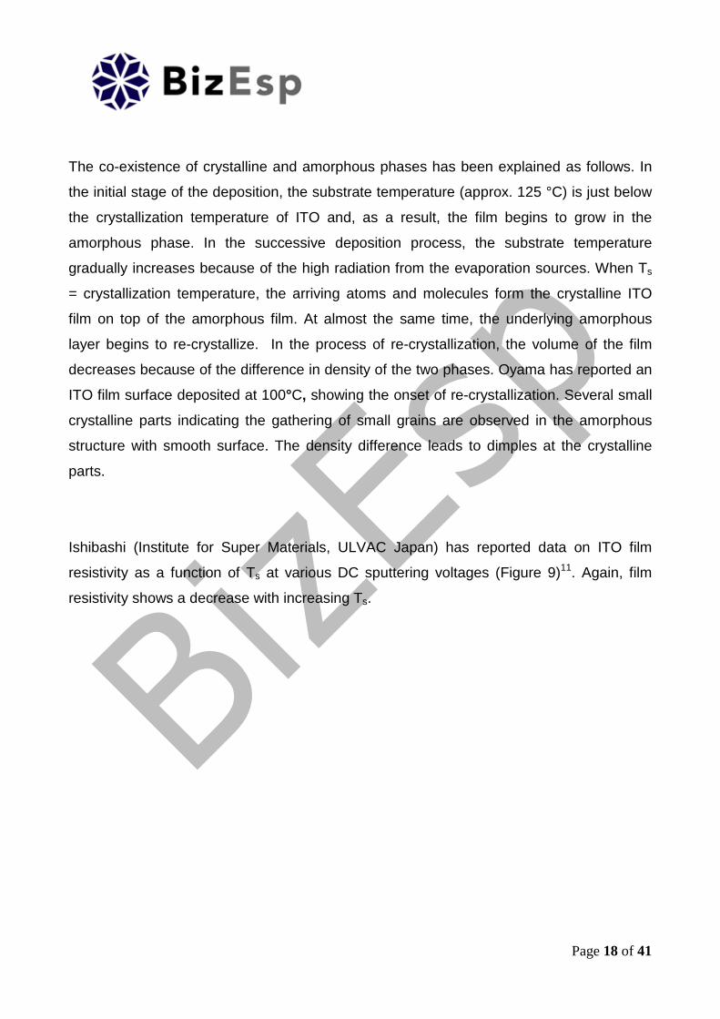
Ishibashi (Institute for Super Materials, ULVAC Japan) has reported data on ITO film
resistivity as a function of Ts at various DC sputtering voltages (Figure 9)11. Again, film
resistivity shows a decrease with increasing Ts.
Page 19 of 41
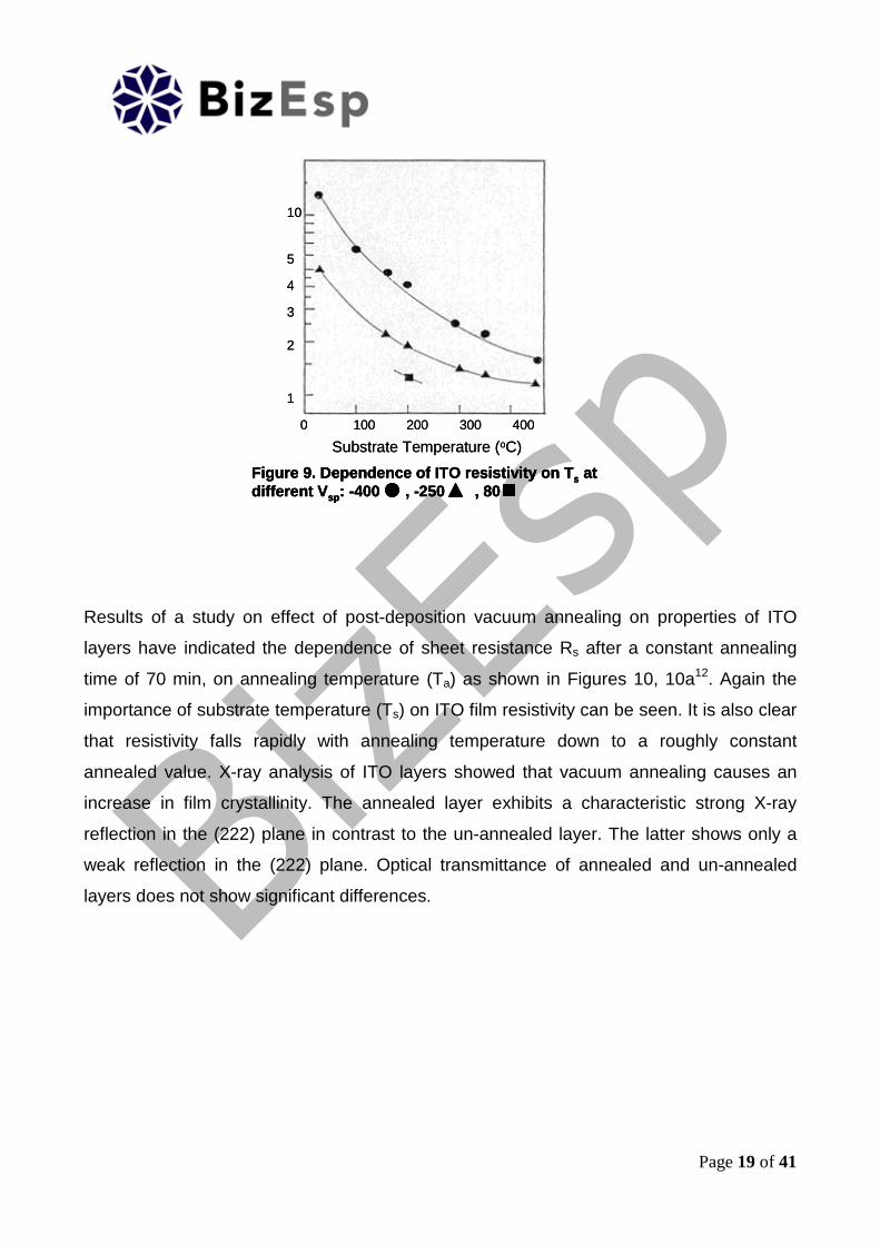
Results of a study on effect of post-deposition vacuum annealing on properties of ITO
layers have indicated the dependence of sheet resistance Rs after a constant annealing
time of 70 min, on annealing temperature (Ta) as shown in Figures 10, 10a12. Again the
importance of substrate temperature (Ts) on ITO film resistivity can be seen. It is also clear
that resistivity falls rapidly with annealing temperature down to a roughly constant
annealed value. X-ray analysis of ITO layers showed that vacuum annealing causes an
increase in film crystallinity. The annealed layer exhibits a characteristic strong X-ray
reflection in the (222) plane in contrast to the un-annealed layer. The latter shows only a
weak reflection in the (222) plane. Optical transmittance of annealed and un-annealed
layers does not show significant differences.
Substrate Temperature (oC)
0 100 200 300 400
1
2
3
4
5
10
Figure 9. Dependence of ITO resistivity on Ts atdifferent Vsp: -400 , -250 , 80
Substrate Temperature (oC)
0 100 200 300 400
1
2
3
4
5
10
Figure 9. Dependence of ITO resistivity on Ts atdifferent Vsp: -400 , -250 , 80Figure 9. Dependence of ITO resistivity on Ts atdifferent Vsp: -400 , -250 , 80

Page 20 of 41
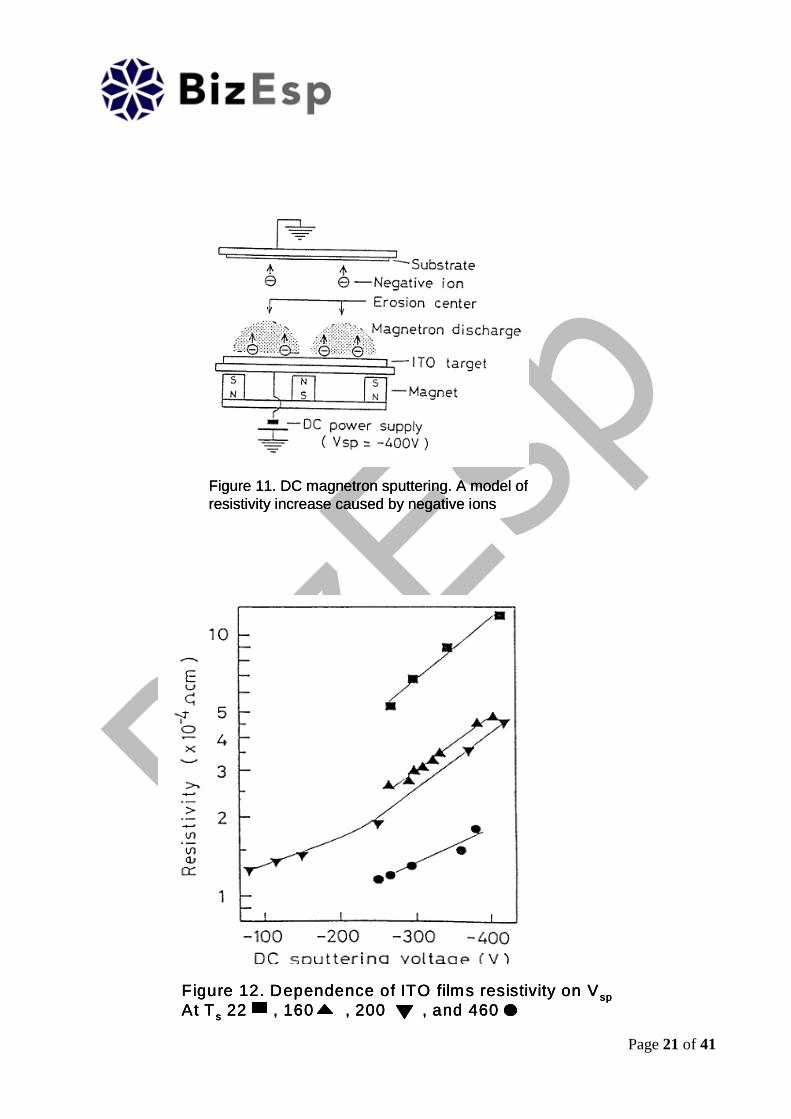
EFFECT OF SPUTTERING VOLTAGE (V)
Ishiibashi has reported on low resistivity and high transmittance ITO film deposited on
glass by DC magnetron sputtering11. The set-up used is depicted in Figure 11. The results
obtained at a VSsp of -370 V at Ts 22, 200, and 350°C are shown in Figure 12.
Figure 10a. XRD pattern of ITOlayer deposited onto glass substrate(Ts = 420K) before (a) and after(b) annealing (ta = 90min Ta=640K)
50 40 30 20
2
Inte
nsity
Figure 10a. XRD pattern of ITOlayer deposited onto glass substrate(Ts = 420K) before (a) and after(b) annealing (ta = 90min Ta=640K)
50 40 30 20
2
Inte
nsity
400 500 600 700400
500
1000
1500
2000
500 600 700
Ta (K)
Rs
(/)
Figure 10. Dependence of ITOSheet resistance (after 760minspost-deposition anneal) onaneealingtemperature (Ta) for films depositedat various Ts
400 500 600 700400
500
1000
1500
2000
500 600 700
Ta (K)
Rs
(/)
400 500 600 700400
500
1000
1500
2000
500 600 700
Ta (K)
Rs
(/)
Figure 10. Dependence of ITOSheet resistance (after 760minspost-deposition anneal) onaneealingtemperature (Ta) for films depositedat various Ts
Page 21 of 41
Figure 12. Dependence of ITO films resistivity on V sp
At T s 22 , 160 , 200 , and 460Figure 12. Dependence of ITO films resistivity on V sp
At T s 22 , 160 , 200 , and 460Figure 12. Dependence of ITO films resistivity on V sp
At T s 22 , 160 , 200 , and 460
Figure 11. DC magnetron sputtering. A model ofresistivity increase caused by negative ionsFigure 11. DC magnetron sputtering. A model ofresistivity increase caused by negative ions

Page 22 of 41
As discussed earlier, the effect of Ts on resistivity can be ascribed to improved crystallinity
of films. Another point to note is that at each Ts, the thin film directly above the erosion
area shows higher resistivity than the film at other positrons. Ishibashi has attributed the
increase of resistivity to ITO film damage caused by impinging negative ions (Figure 11).
Negative ions. e.g. oxygen ions, generated in target surface are accelerated by the
negative potential in almost direct angle from the target, and collide with the substrate to
cause ITO film damage. The negatively charged oxygen ion density is high on the erosion
areas because, in magnetron discharge, the plasma is concentrated on the erosion area.
Therefore, film damage by negative ions is larger above the erosion area and so is the
resistivity. Above the centre of the target, however, there are less negative ions colliding
with the film and resistivity is lower. It follows, therefore, that a lower collision energy of
negative ions could reduce the resistivity of ITO film. Ishibashi has reported on ITO films
deposited at a lower voltage of -110 V (Figure 13).
Position (mm)-50 0 50
Re
sis
tivi
ty(x
10
-4
cm
1
2
3
4
5
Figure 13. Resistivities of ITO films deposited on fixed 200C substratesAt each plasma position (see also Figure 11) when Vs were –370 , -250 ,and –110
Position (mm)-50 0 50
Re
sis
tivi
ty(x
10
-4
cm
1
2
3
4
5
Figure 13. Resistivities of ITO films deposited on fixed 200C substratesAt each plasma position (see also Figure 11) when Vs were –370 , -250 ,and –110
Figure 13. Resistivities of ITO films deposited on fixed 200C substratesAt each plasma position (see also Figure 11) when Vs were –370 , -250 ,and –110
Page 23 of 41
The results show a decrease in resistivity at each substrate temperature and no increase
of resistivity directly above erosion area. Evidently, lowering Vsp leads to a decrease in ITO
film damage caused by negative ions. Variation of resistivity with plasma positions at Vsp -
370, -250. and -110 V (Figure 13) shows a reduction in resistivity, at all plasma positions,
with lower Vsp. Furthermore, the degree of resistivity increase above the erosion area
becomes smaller. Thus a lower Vsp is very effective in reducing ITO film resistivity.
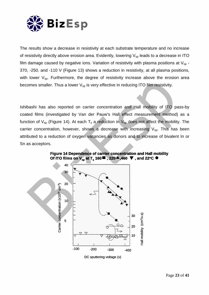
Ishibashi has also reported on carrier concentration and Hall mobility of ITO pass-by
coated films (investigated by Van der Pauw’s Hall effect measurement method) as a
function of Vsp (Figure 14). At each Ts a reduction in Vsp does not affect the mobility. The
carrier concentration, however, shows a decrease with increasing Vsp. This has been
attributed to a reduction of oxygen vacancies as donors and to increase of bivalent In or
Sn as acceptors.
DC sputtering voltage (v)
-100 -200 -300 -400
10
20
30
Hall
mobili
ty(c
m2/v
.s)
Carr
ier
concentr
atio
n(x
10
20
cm-3
)
5
10
20
30
40
Figure 14 Dependence of carrier concentration and Hall mobilityOf ITO films on Vsp at Ts 160 , 220 ,460 , and 22oC
DC sputtering voltage (v)
-100 -200 -300 -400
10
20
30
Hall
mobili
ty(c
m2/v
.s)
Carr
ier
concentr
atio
n(x
10
20
cm-3
)
5
10
20
30
40
Figure 14 Dependence of carrier concentration and Hall mobilityOf ITO films on Vsp at Ts 160 , 220 ,460 , and 22oCFigure 14 Dependence of carrier concentration and Hall mobilityOf ITO films on Vsp at Ts 160 , 220 ,460 , and 22oC
Page 24 of 41
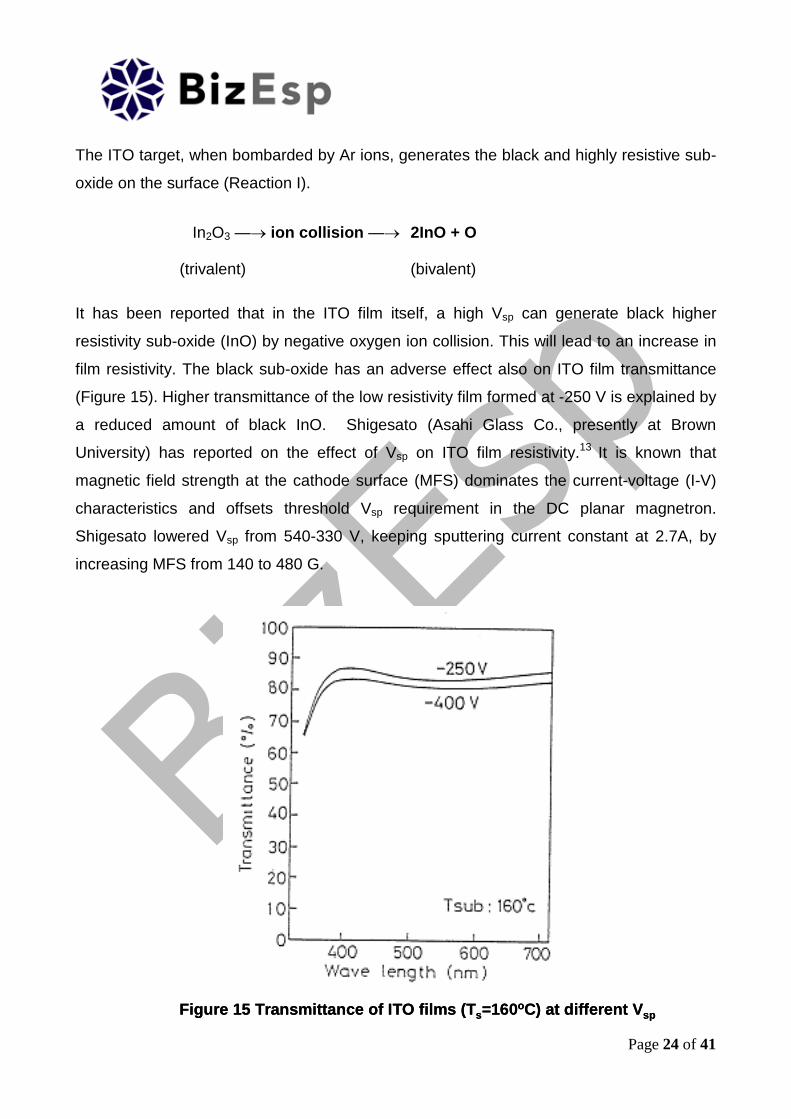
The ITO target, when bombarded by Ar ions, generates the black and highly resistive sub-
oxide on the surface (Reaction I).
In2O3 — ion collision — 2InO + O
(trivalent) (bivalent)
It has been reported that in the ITO film itself, a high Vsp can generate black higher
resistivity sub-oxide (InO) by negative oxygen ion collision. This will lead to an increase in
film resistivity. The black sub-oxide has an adverse effect also on ITO film transmittance
(Figure 15). Higher transmittance of the low resistivity film formed at -250 V is explained by
a reduced amount of black InO. Shigesato (Asahi Glass Co., presently at Brown
University) has reported on the effect of Vsp on ITO film resistivity.13 It is known that
magnetic field strength at the cathode surface (MFS) dominates the current-voltage (I-V)
characteristics and offsets threshold Vsp requirement in the DC planar magnetron.
Shigesato lowered Vsp from 540-330 V, keeping sputtering current constant at 2.7A, by
increasing MFS from 140 to 480 G.
Figure 15 Transmittance of ITO films (Ts=160oC) at different VspFigure 15 Transmittance of ITO films (Ts=160oC) at different Vsp
Page 25 of 41
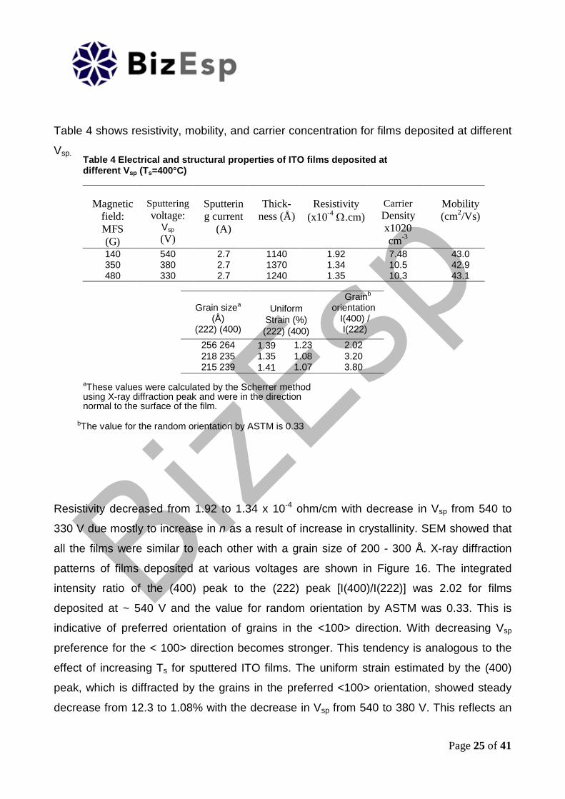
Table 4 Electrical and structural properties of ITO films deposited atdifferent Vsp (Ts=400°C)
Magneticfield:MFS(G)
Sputteringvoltage:
Vsp
(V)
Sputtering current
(A)
Thick-ness (Å)
Resistivity(x10-4 .cm)
CarrierDensityx1020cm-3
Mobility(cm2/Vs)
140 540 2.7 1140 1.92 7.48 43.0350 380 2.7 1370 1.34 10.5 42.9480 330 2.7 1240 1.35 10.3 43.1
Grain sizea
(Å)(222) (400)
UniformStrain (%)(222) (400)
Grainb
orientationI(400) /I(222)
256 264 1.39 1.23 2.02218 235 1.35 1.08 3.20215 239 1.41 1.07 3.80
aThese values were calculated by the Scherrer methodusing X-ray diffraction peak and were in the directionnormal to the surface of the film.
bThe value for the random orientation by ASTM is 0.33
Table 4 shows resistivity, mobility, and carrier concentration for films deposited at different
Vsp.
Resistivity decreased from 1.92 to 1.34 x 10⁻⁴ ohm/cm with decrease in Vsp from 540 to
330 V due mostly to increase in n as a result of increase in crystallinity. SEM showed that
all the films were similar to each other with a grain size of 200 - 300 Å. X-ray diffraction
patterns of films deposited at various voltages are shown in Figure 16. The integrated
intensity ratio of the (400) peak to the (222) peak [I(400)/I(222)] was 2.02 for films
deposited at ~ 540 V and the value for random orientation by ASTM was 0.33. This is
indicative of preferred orientation of grains in the <100> direction. With decreasing Vsp
preference for the < 100> direction becomes stronger. This tendency is analogous to the
effect of increasing Ts for sputtered ITO films. The uniform strain estimated by the (400)
peak, which is diffracted by the grains in the preferred <100> orientation, showed steady
decrease from 12.3 to 1.08% with the decrease in Vsp from 540 to 380 V. This reflects an

Page 26 of 41
increase in crystallinity of ITO films. The higher
crystallinity results in a decrease in concentration of electrically inactive dopants (Sn or
oxygen vacancy) trapped at crystalline defects (caused by bombardment of high energy
negative oxygen ions during deposition) and hence increase electrically active species
inside each grain. By using a stronger magnetic field, plasma impedance is decreased and
low damaged films are deposited with a low resistivity of 1.34 x 10⁻⁴ ohm/cm.
0
1.0
0
1.0
1.0
Inte
nsity
(kcps)
20 30 40 50 60 70
Figure 16. XRD patterns of ITO films (thickness 1200Å)deposited by DC magnetron sputtering at different Vsp
0
1.0
0
1.0
1.0
Inte
nsity
(kcps)
20 30 40 50 60 700
1.0
0
1.0
1.0
Inte
nsity
(kcps)
20 30 40 50 60 70
Figure 16. XRD patterns of ITO films (thickness 1200Å)deposited by DC magnetron sputtering at different Vsp

Page 27 of 41
RECENT MODIFICATIONS OF SPUTTERING PROCEDURES
a) Face Target Sputtering (FTS)
One point in common amongst the sputtering methods discussed earlier is that either the
substrate has to be heated above 200 -400 °C during deposition or post-deposition
annealing at > 300 °C in controlled atmospheres is necessary. However, for certain
applications, the use of an elevated substrate or post-deposition annealing temperature is
undesirable. Lee et al. (Mitsubishi Materials Corporation. Japan) have reported the
deposition at low temperature (23°C) and pressure (0.1 - 10mTorr) of highly transparent
and conductive ITO films by the face transfer sputtering (FTS) process in pure argon14.
The FTS system used was FTS-C3 (Osaka Vacuum) with a 140mm distance between the
targets (Figure 17) (125 mm diameter, In2O3 : SnO2 90:10%Wt., 70% density made by
Mitsubishi Materials Corporation, Japan). A RF discharge (13.56 MHz) of 200W was used
and the targets were pre-sputtered for 15 mm before deposition. As the magnetic field of
150 Oe acts perpendicular to target planes, the plasma is confined between the two
targets. Thus, bombardment damage of the substrate and growing ITO film by high energy
particles such as electrons and negative ions is largely avoided.
In the FTS system, the ITO thin film parameters are almost temperature independent.

Page 28 of 41
Figure 18 shows XRD patterns of films deposited at various Ts and at pressures of 10
mTorr and 1 mTorr. At 10 mTorr, the usual trend of increasing crystallinity with Ts is
observed. But the effect of Ts is completely eclipsed by a change in pressure and the films
deposited at 1 mTorr are amorphous even at Ts 300°C. At 10 mTorr / Ts =200 & 300 °C, a
grainy surface is obtained. At 1 mTorr / Ts = 200 & 300 °C, a plate-like structure is
obtained and at Ts = 300 °C a grainy surface, with occasional spherical particles ranging
from 0.2 to 0.3 mm, is observed at T, 200 °C. When the sputtering pressure is lowered to
0. 1 mTorr and Ts set at 300 °C, a rough grainy surface results. If Ts is lowered to 200 °C a
surface with pin-holes results. Thus, low pressure facilitates formation of pin-holes. This
effect of pressure has not been rationalised by Lee et al.
The
resistivity, carrier concentration and mobility of ITO films deposited at different Ts under
various pressures are shown in Figure 19. At 0.1 mTorr and 1 mTorr there is no significant

Page 29 of 41
Figure 19Figure 19
change in resistivity and carrier concentration with Ts. All the films reported by Lee et al.
have low carrier mobility and (u) varies from about 15 to 44 cm2/Vs. In the FTS method of
Lee et al., the transmittance of tile films between 400 - 900 nm does not vary significantly
with either ps or Ts. Since the films change from an amorphous to a textured crystalline
phase at ps 10 mTorr, it indicates that transmittance does not depend on the degree of
crystallinity or orientation of films or surface morphology. Whether the film is covered with
pin-holes or consists of fine grains, transmittance does not change significantly.

Page 30 of 41
As discussed earlier, it has been reported by various authors that ITO film properties are
improved by adding a small amount of oxygen to the sputtering system during deposition.
Lee et al. have reported, however, that the presence of oxygen in the FTS system is
detrimental to the electrical properties of ITO thin films. Lee et al. have suggested that with
increased oxygen partial pressure, the concentration of oxygen vacancies in the film is
reduced. As the conductivity of ITO results from oxygen deficiency and a higher valent
cation doping of In2O3, a decrease in charge carriers. Therefore, resistivity increases as
oxygen is added during sputtering. The problem with this explanation is that if it was
correct then a similar phenomenon should be observed in normal sputtering procedures.
Why should it be limited to FTS? To conclude, the FTS system can be used to deposit
films at low Ts which are comparable in their electrical properties to films deposited at
higher Ts in normal sputtering procedures.
HIGH RATE INDIUM TIN OXIDE SPUTTERING
Most of the studies reported in the literature on high rate ITO sputtering have used DC
planar magnetron reactive sputtering. As discussed earlier, reactive sputtering is difficult to
control. In high rate large-scale deposition, the main problem is that as the reactive gas
flow is increased, a transition occurs at the target surface from a metallic to a poisoned
(oxide) target surface. Sputtering from a metallic target surface leads to high deposition
rates. It is therefore desirable to operate the magnetron with a largely metallic target
surface while having sufficient reactive gas pressure at the substrate to form the film.
For stable production of ITO film, it is necessary to have at the substrate surface:
a) a constant metal flux
b) a constant arrival rate of oxygen
c) a constant utilization of oxygen.
These parameters are inter-related in a way that can lead to instability. The metal flux
depends on the state ~ the target which depends on the total reactive gas pressure (Po2)

Page 31 of 41
F ig u r e 2 0 M e c h a n is m o f in s ta b i l i ty in re a c t iv e D C m a g n e tr o nF ig u r e 2 0 M e c h a n is m o f in s ta b i l i ty in re a c t iv e D C m a g n e tr o n
The arrival rate of oxygen at the substrate also depends on (Po2). It follows therefore that
(Po2) is a very important process parameter.
PRESSURE STABILITY IN DC REACTIVE MAGNETRON SPUTTERING
Spencer et al. (Loughborough university of Technology, UK) have reported on the effect of
(Po2) on target poisoning in reactive DC magnetron sputtering15 At the target, the surface is
constantly being poisoned (oxide build-up) and sputtered clean. When the poisoning rate
exceeds the cleaning rate, a poisoned surface exists (leading to decrease in 02
consumption caused by a decrease in metal flux, and increase in (Po2) and with increase in
(Po2) the proportion of poisoned surface increases. This cycle continues until the target is
completely poisoned and then the metal flux remains roughly constant (Figure 21a).

Page 32 of 41
At the substrate, at low reactive gas (Po2) the formation of ITO is limited by the arrival rate
and utilization of the reactive gas and so a metal rich film is formed. As the reactive gas
pressure is increased, the arrival rate of reactive gas increases and the film becomes less
Page 33 of 41
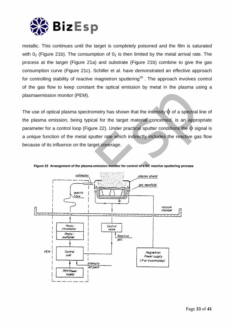
Figure 22 Arrangement of the plasma-emission monitor for control of a DC reactive sputtering processFigure 22 Arrangement of the plasma-emission monitor for control of a DC reactive sputtering process
metallic. This continues until the target is completely poisoned and the film is saturated
with 02 (Figure 21b). The consumption of 02 is then limited by the metal arrival rate. The
process at the target (Figure 21a) and substrate (Figure 21b) combine to give the gas
consumption curve (Figure 21c). Schiller et al. have demonstrated an effective approach
for controlling stability of reactive magnetron sputtering16 . The approach involves control
of the gas flow to keep constant the optical emission by metal in the plasma using a
plasmaemission monitor (PEM).
The use of optical plasma spectrometry has shown that the intensity of a spectral line of
the plasma emission, being typical for the target material concerned, is an appropriate
parameter for a control loop (Figure 22). Under practical sputter conditions the signal is
a unique function of the metal sputter rate which indirectly includes the reactive gas flow
because of its influence on the target coverage.

Page 34 of 41
Figure 23. In-line sputtering plant for double-sided coating of glass substrates with reactive DC magnetronsputtering process controlled by PEM monitor at both sources.Figure 23. In-line sputtering plant for double-sided coating of glass substrates with reactive DC magnetronsputtering process controlled by PEM monitor at both sources.
As shown in Figure 23, after the plasma emission has been coupled out in the vicinity of
the target with the aid of a suitable collimator, it is passed on via a fibre-optics system and
a monochromator. The resultant intensity of a characteristic spectral line is converted into
a signal by means of photomultiplier and applied to the PEM controller as the actual
value. With the aid of a piezoelectric valve, the PEM controller then adjusts the reactive
gas flow to keep the intensity constant. The system shown in Figure 29 has been used for
ITO deposition. It is a HZ5-04 in-line sputter plant from VEB Electromat, Dresden
(Germany) in which double sided coating is carried out to increase plant productivity. Two
PPS-5 magnetron sources with a target size 610 x 160 mm are arranged below and above
the substrate carrier of 500 x 500 mm designed to accommodate glass substrate. Each
source is equipped with the power supply unit for the sputter source, the reactive gas inlet
and manifold, the fibre-optics system and the PEM controller. The equipment can give
deposition rates of up to 10 nm/s.
Other less important problems encountered in large-scale reactive sputtering are:
Page 35 of 41
Arcing
Gillery (PPG Industries Inc.. USA) has reported that in a large system, the whole power of
25 kW power supply can be diverted into an arc17. The arcs can adversely effect the
equipment and also the cathode surface (localized melting due to a hot spot).
Nodule Formation
As explained earlier, ITO targets when sputtered by argon ions, generate black and high
resistivity sub-oxide On the surface:
In2O3 — ion collision — 2InO + O
High resistivity oxide sputters at a lower rate and gives rise to nodules. High resistivity
impurities in the target matrix can have a similar effect. Gehman et al. (Leybold
Materials Inc.. USA) have suggested that there is a correlation between oxide target
density and nodule population18 . Their results indicate that dense targets have lower
tendency for nodule formation. The reasons for this are not understood. Formation of
nodules has also been observed by Czukor et al. (Courtaulds Performance Films. CA,
USA) in DC magnetron sputter roll coater reactive sputtering using a metallic alloy target.19
One of the targets studied by Czukor developed a layer of black, glassy nodules on the
periphery of the magnetron racetrack. Czukor et al. report that the nodules have a much
lower sputtering yield than the unmodified metallic target material. It is likely that nodules
observed by Czukor are composed of the lower oxide of indium.
CONCLUSIONS
The market for products utilizing ITO thin films is continuing to grow, despite an often
ambivalent world economy, due to increasing demand for LCDs. This trend is likely to
continue, for example with the growing popularity of lap-top computers, flat screen desk-
top monitors, hand-held gadgets and flat-screen TV’s, and the future for ITO
manufacturers looks rosy. The only future threat to ITO thin film market may come from
Page 36 of 41
cheaper TCO materials such as doped zinc oxide films, provided that stability of electro--
optical properties in zinc oxide films can be attained.
Currently, sputtering is the main method for ITO thin film production. Reactive sputtering
using In:Sn alloy target has been a popular method as shown by the plethora of
publications on the subject. This is attributed to the unavailability and expense of high
quality oxide targets combined with the difficulty of bonding oxide targets to metal backing
plates. The process of reactive sputtering is, however, very difficult to control. This method
therefore has declined in popularity with increasing availability of high quality ITO targets.
Non-reactive sputtering using ITO targets is now the most popular method for ITO thin film
deposition due to excellent progress on: (1) optimizing target performance parameters, (2)
solving difficulties encountered in non-reactive sputtering, for example, nodule formation.
and (3) developing suitable target bonding materials.
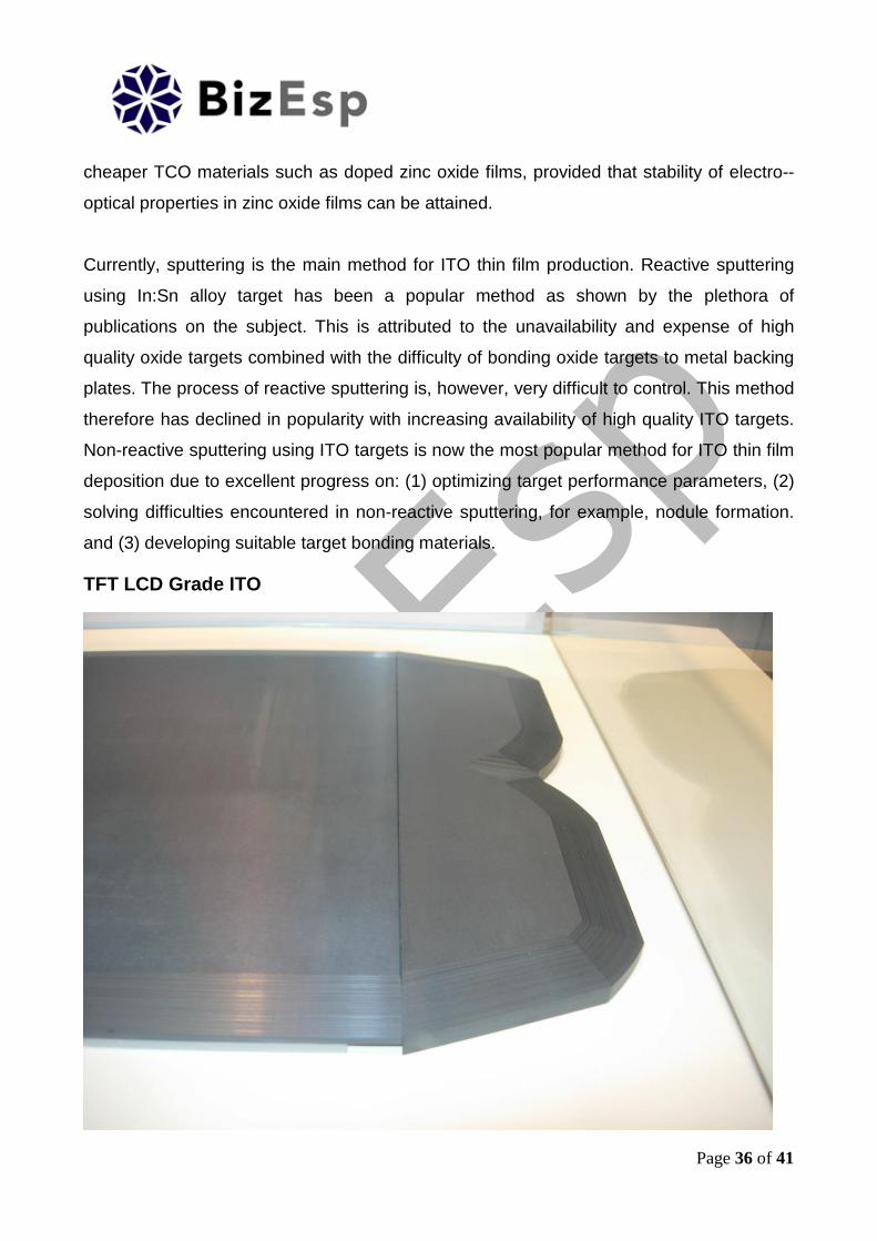
TFT LCD Grade ITO
Page 37 of 41
REFERENCES
1. ‘Handbook of Thin Film Technology’, Eds. L. I. Maissel and R. Glang, McGraw Hill
Book Company, 1970, New York.
2. K. L. Chopra et a!., Transparent Conductors - A Status Review, Thin Solid
Films, 1983, 1Q~, 1.
3. H. Oechsner, Sputtering - A Review of Some Recent Experimental and
Theoretical Aspects, Applied Physics, 1975. ~, 185.
4. M. Konurna, Film Deposition by Plasma Techniques, Springer, 1992,
Heidelberg, ISBN 3-540-54057-1.
5. W. D. Westwood, Reactive Sputtering, in Physics of Thin Films, M. H. Francombe
and J. L. Vossen, Volume 14, Academic Press Inc. (London) Ltd., 1989, ISBN 0-
12- 533014-6.
6. J. L. Vossen, Transparent Conducting Films, in Physics of Thin Films, 1977,
Volume~, 1.
7. Superconductor Industry, 1993, Volume 6, No. 2, 45.
8. Y. Shigesato et al., Crystallinity and Electrical Properties of Till-Doped Indium
Oxide Films Deposited by DC Magnetron Sputtering, Applied Surface Science,
1991, 48/49, 269.
9. T. Oyama et al., Low Resistance Indium Tin Oxide Films on Large Scale Glass
Substrate, J. Vac. Sci. Technol. A, 1992, jQ, 4, 1682. (b) A. Hjortsberg et al.,
Transparent and Heat Reflecting Indium Tin Oxide Films Prepared By
Reactive Electron Beam Evaporation. Thin Solid Films, 1982, 90, 323. (c) M.
Mizuhashi, Electrical Properties of VaCLJUn1 Deposited Indium Oxide and Indium
Page 38 of 41
Tin Oxide Films, Thin Solid Films, 1980. 70, 91 and refs. therein. (d) M.
10. Mizuhashi, Electrical Properties of Post Oxidized In.,01:Sn Films, Thin Solid
Films, 1981, 76, 97.
11. R. Latz et al., High Conducting Large Area Indium Tin Oxide Electrodes for
Displays Prepared by DC Magnetron Sputtering, Jap. J. AppI. Physics, 1991,
30, 2A, L149.
12. S. Ishibashi et al., Low Resistivity indium Tin Oxide Transparent Conductive Films.
Effect of Sputtering Voltage ~n Electrical Property of Films, J. Vac. Sd. Technol. A,
1990, 8, 3, 1403 and refs. therein.
13. M. Libra and L. Bardos, Effect of Post-Deposition Vacuum Annealing of
Properties of ITO Layers, Vacuum, 1988, 38, 6, 455.
14. Y. Shigesato et al., Electrical avid Structural Properties of Low Resistivity TIn
Doped Indium Oxide Films, J. Appl. Physics, 1992, 7 1(7), 3356 and refs.
therein.
15. W. K. Lee et al., Low Pressure and Temperature Deposition of Transparent
Conductive Indium Timi Oxide Films by the Face Target Sputtering Process,
Thin Solid Films, 1993, 224, 105.
16. A.G. Spencer et al., Pressure Stability in Reactive Magnetron Sputtering, Thin
Solid Films, 1988, 158, 141.
17. S. Schiller et al., Reactive DC High Rate Sputtering As Production
Technology, Surface and Coatings Technology, 1987, 33, 405 and refs.
therein.
18. F. H. Gillery, Large Scale Sputtering of indium Tin Oxide, J. Vac. Sci. Technol.,

Page 39 of 41
1978, 15(2), 306.
19. B. L. Gehman, Influence of Manufacturing Process of Indium Tin Oxide
20. Sputtering Targets on Sputtering Behaviour, Thin Solid Films, 1992, 220, 333.
21. J. Czukor et al., The Effects of Process Conditions on the Quality and
Deposition Rate of Sputtered Indium Tin Oxide Coatings. Society of Vacuum
Coaters, 34th Annual Technical Conference Proceedings, 1991. 190.
Page 40 of 41
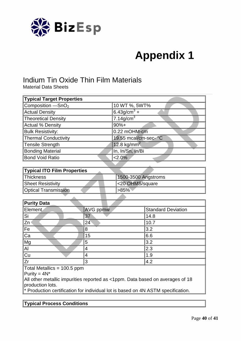
Indium Tin Oxide Thin Film MaterialsMaterial Data Sheets
Typical Target Properties
Composition —SnO2 10 WT %, 5WT%
Actual Density 6.43g/cm3 +
Theoretical Density 7.14g/cm3
Actual % Density 90%+
Bulk Resistivity: 0.22 mOHM-cm
Thermal Conductivity 19.55 mcal/cm-sec- °C
Tensile Strength 12.8 kg/mm2
Bonding Material In, In/Sn, In/Bi
Bond Void Ratio <2.0%
Typical ITO Film Properties
Thickness 1500-3500 Angstroms
Sheet Resistivity <20 OHMS/square
Optical Transmission >85%
Purity Data
Element AVG ppmw Standard Deviation
Si 37 14.8
Zn 24 10.7
Fe 8 3.2
Ca 15 6.6
Mg 5 3.2
Al 4 2.3
Cu 4 1.9
Zr 3 4.2
Total Metallics = 100.5 ppmPurity = 4N*All other metallic impurities reported as <1ppm. Data based on averages of 18production lots.* Production certification for individual lot is based on 4N ASTM specification.
Typical Process Conditions
Appendix 1

Page 41 of 41
Power Density 3.0-7.0 W/cm2
Operating Pressure 3-5mTorr
Process Gas Flow 30-100 SCCM
O2 Partial pressure % 0-2%
Target/Substrate Dist. 1.5-4.0"
Substrate Temperature 20°C-350°C
Note: These typical process conditions are meant only as a guide to the use ofthese materials and are not indicative of the optimum process conditions you canachieve with your system