Towards Logic Programming as a Service: Experiments in tuProlog

UNIVERSITY OF OTTAWA
FACULTY OF ENGINEERING
SCHOOL OF INFORMATION TECHNOLOGY AND ENGINEERING
ITI1100
Laboratory Experiments
A. Karmouch, V. Groza and A. Al-Dhaher
Winter 2008

ELG1100 Introduction to Electrical and Computer Engineering Lab Manual
TABLE OF CONTENTS
GENERAL GUIDELINES Laboratory instructions Laboratory report format
GENERAL INTRODUCTION Digital Test Equipment Combinational Logic Circuits
LABORATORY EXPERIMENTS Lab 1: Logic gates Lab 2: Boolean logic Lab 3: Decoders, displays and multiplexers Lab 4: Adders (using Altera) Lab 5: Flip Flops Lab 6: Counters (using Altera)
University of Ottawa, School of Information Technology and Engineering 2

ELG1100 Introduction to Electrical and Computer Engineering Lab Manual
LABORATORY INSTRUCTIONS Attendance Please be available at the beginning of the laboratory session. Lab sessions will start by taking the attendance, and then there will be a 15-20 minute introduction in which the TAs will explain the experiment. During this time you may ask your TAs any questions about the experiment. Absence from any lab session will result in a zero lab mark and the report will not be accepted. Working group Laboratory groups will consist of two students only. Students are required to stay in the same group and with the same TA for the whole semester. Every group performing the experiment is required to record their data on page(s) and this should be seen and signed by the TA. The data should be attached to the submitted report. One lab report is expected from each group after each lab. The lab report should be prepared according to the guidelines outlined in the next page. If you are in doubt, please ask your TA. Reports are due one week from the date of performing the experiments. Marked reports will be returned in the following lab session. Late submission of lab reports will result in a 5% deduction for each late day. Tools Each group should have the following: (1) breadboard (1) pair of pliers (1) pair of side-cutter/wire strippers (1) small screwdriver General recommendations
• Please do not place your coat, bags etc. on the bench.
• It is highly recommended that you observe caution in working with equipment to avoid any risk to yourself and to your partner or cause damage to the lab or lab equipment.
• Have your circuit checked by the TA before you switch it ON.
• Make sure you clean your bench before you leave. Any trash should be put in its place.
• In order to finish your experiment in the time allotted, it is advisable that you stay at your
workbench and not wonder around the lab.
University of Ottawa, School of Information Technology and Engineering 3

ELG1100 Introduction to Electrical and Computer Engineering Lab Manual
LABORATORY REPORT FORMAT Cover page A cover page should include the title of the experiment, student names and numbers and the date in which the experiment was performed. Objectives State the main objectives and all sub-objectives. Also anystate laws/rules that will be verified. Equipments and components used List all instruments and components used in the experiment. Clearly mention their model/type. Circuit diagram Draw circuit diagrams to be tested or used in the lab with all the values and component types used. Experimental data and data processing Using tables, show experimental data referring to procedure step number. Also, present the data in the same order as the procedure. Perform calculations using measured data. All circuit diagrams must be drawn using a ruler. Comparison of expected data and experimental data Perform a side-by-side comparison of expected and experimental data in a table and highlight or circle major deviations. Discussion and conclusion Discuss matching of expected and experimental data in general and state what laws have been verified, what sub-objectives have been met and try to find logical explanation for major deviations. Give summary of results in tabular form if necessary and state whether main objectives were met. Laboratory data sheets Include with the report the laboratory data sheet signed by the TA who supervised the experiment.
University of Ottawa, School of Information Technology and Engineering 4

ELG1100 Introduction to Electrical and Computer Engineering Lab Manual
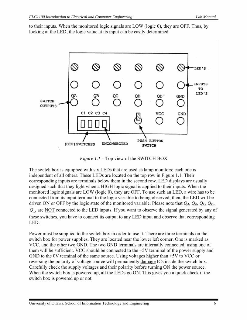
GENERAL INTRODUCTION DIGITAL TEST EQUIPMENT Breadboarding and testing equipment used with digital circuits generally include the following functions: Power Supply The power supply provides a regulated +5 volts DC voltage to be used to power TTL integrated circuits. Note that some units may also contain additional fixed voltages or a variable DC power source for other types of circuits. Lamp Monitors The lamp monitors indicate the voltage level at various points in the digital circuit being tested. The lamp monitors will light when a digital “high” voltage is applied to them. Logic Switches The logic switches input either of the two logic levels (voltages) to the circuit being tested. A switch in the ‘down’ position will provide a logic low voltage (approximately 0 volts), while a switch in the up position will provide a logic high voltage (approximately + 5 volts). Pushbuttons or pushers A pushbutton provides a momentary “bounce free” logic input to the test circuit. Pulsers that are provided on some testing systems produce a short duration (narrow) pulse or change in the logic level of the pulser’s output. ClockThe clock provides a variable frequency pulse waveform that can be used for the timing control of some digital circuits. Switch Box
Four toggle logic switches in one dual-in-line package (DIP) are provided on the switch box (see Figure 1.1 for a top view of the switch box). Only the first three switches Cl, C2 and C3 are connected to terminals (marked QA, QB and QC respectively ) on the box, to providing logic signals; e.g., if Cl is ON, QA will present a high voltage (i.e., a logic 1) and if it is OFF, QA will exhibit a low voltage (i.e. a logic 0). The switch C4 is totally unconnected and useless.
There is also a push-button switch on the switch box. When pushed, it will provide a single 20 ms wide pulse. The positive version of this pulse is generated at the terminal marked QD, while its complemented version can be obtained from DQ . QD is normally low until the push-button is pressed, then it goes high for 20 ms and then goes back low again.
The three toggle switches will provide you with three independent logic variables to be used as inputs in your circuits. The push-button switch can be used when pulses are needed for clocking or counting purposes.
The switch box is equipped with light-emitting diodes (LEDs) that are used as lamp monitors. LED displays are usually designed such that the light is ON when a HIGH logic signal is applied
University of Ottawa, School of Information Technology and Engineering 5
ELG1100 Introduction to Electrical and Computer Engineering Lab Manual
to their inputs. When the monitored logic signals are LOW (logic 0), they are OFF. Thus, by looking at the LED, the logic value at its input can be easily determined.
Figure 1.1 – Top view of the SWITCH BOX
The switch box is equipped with six LEDs that are used as lamp monitors; each one is independent of all others. These LEDs are located on the top row in Figure 1.1. Their corresponding inputs are terminals below them in the second row. LED displays are usually designed such that they light when a HIGH logic signal is applied to their inputs. When the monitored logic signals are LOW (logic 0), they are OFF. To use such an LED, a wire has to be connected from its input terminal to the logic variable to being observed; then, the LED will be driven ON or OFF by the logic state of the monitored variable. Please note that QA, QB, QB C, QD,
DQ are NOT connected to the LED inputs. If you want to observe the signal generated by any of these switches, you have to connect its output to any LED input and observe that corresponding LED.
Power must be supplied to the switch box in order to use it. There are three terminals on the switch box for power supplies. They are located near the lower left corner. One is marked as VCC, and the other two GND. The two GND terminals are internally connected; using one of them will be sufficient. VCC should be connected to the +5V terminal of the power supply and GND to the 0V terminal of the same source. Using voltages higher than +5V to VCC or reversing the polarity of voltage source will permanently damage ICs inside the switch box. Carefully check the supply voltages and their polarity before turning ON the power source. When the switch box is powered up, all the LEDs go ON. This gives you a quick check if the switch box is powered up or not.
University of Ottawa, School of Information Technology and Engineering 6
ELG1100 Introduction to Electrical and Computer Engineering Lab Manual
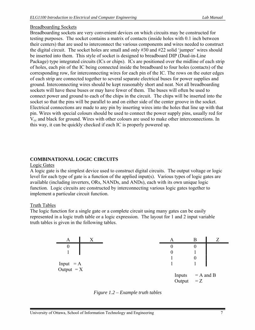
Breadboarding SocketsBreadboarding sockets are very convenient devices on which circuits may be constructed for testing purposes. The socket contains a matrix of contacts (inside holes with 0.1 inch between their centers) that are used to interconnect the various components and wires needed to construct the digital circuit. The socket holes are small and only #30 and #22 solid ‘jumper’ wires should be inserted into them. This style of socket is designed to breadboard DIP (Dual-in-Line Package) type integrated circuits (ICs or chips). ICs are positioned over the midline of each strip of holes, each pin of the IC being connected inside the breadboard to four holes (contacts) of the corresponding row, for interconnecting wires for each pin of the IC. The rows on the outer edges of each strip are connected together to several separate electrical buses for power supplies and ground. Interconnecting wires should be kept reasonably short and neat. Not all breadboarding sockets will have these buses or may have fewer of them. The buses will often be used to connect power and ground to each of the chips in the circuit. The chips will be inserted into the socket so that the pins will be parallel to and on either side of the center groove in the socket. Electrical connections are made to any pin by inserting wires into the holes that line up with that pin. Wires with special colours should be used to connect the power supply pins, usually red for Vcc and black for ground. Wires with other colours are used to make other interconnections. In this way, it can be quickly checked if each IC is properly powered up. COMBINATIONAL LOGIC CIRCUITS Logic GatesA logic gate is the simplest device used to construct digital circuits. The output voltage or logic level for each type of gate is a function of the applied input(s). Various types of logic gates are available (including inverters, ORs, NANDs, and ANDs), each with its own unique logic function. Logic circuits are constructed by interconnecting various logic gates together to implement a particular circuit function. Truth TablesThe logic function for a single gate or a complete circuit using many gates can be easily represented in a logic truth table or a logic expression. The layout for 1 and 2 input variable truth tables is given in the following tables.
A X A B Z 0 0 0 1 0 1
1 0 Input = A 1 1 Output = X
Inputs = A and B Output = Z
Figure 1.2 – Example truth tables
University of Ottawa, School of Information Technology and Engineering 7
ELG1100 Introduction to Electrical and Computer Engineering Lab Manual
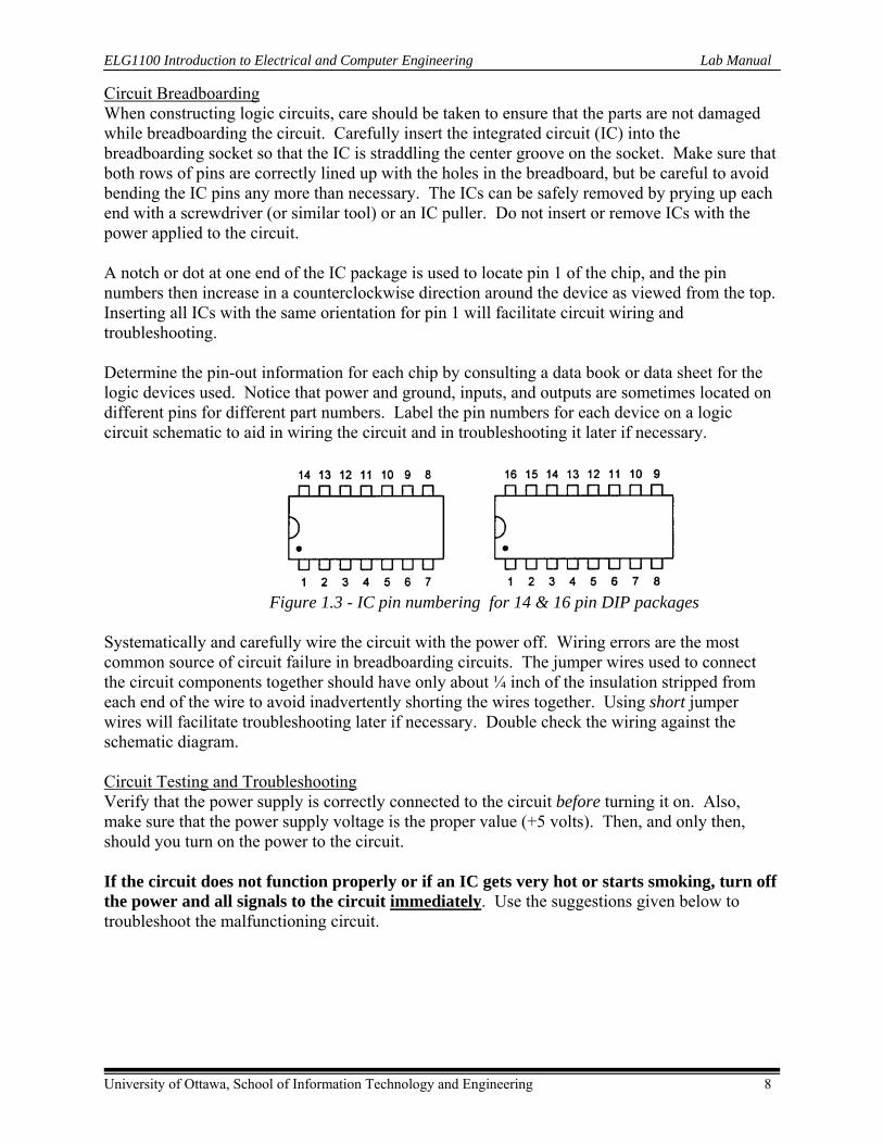
Circuit Breadboarding When constructing logic circuits, care should be taken to ensure that the parts are not damaged while breadboarding the circuit. Carefully insert the integrated circuit (IC) into the breadboarding socket so that the IC is straddling the center groove on the socket. Make sure that both rows of pins are correctly lined up with the holes in the breadboard, but be careful to avoid bending the IC pins any more than necessary. The ICs can be safely removed by prying up each end with a screwdriver (or similar tool) or an IC puller. Do not insert or remove ICs with the power applied to the circuit.
A notch or dot at one end of the IC package is used to locate pin 1 of the chip, and the pin numbers then increase in a counterclockwise direction around the device as viewed from the top. Inserting all ICs with the same orientation for pin 1 will facilitate circuit wiring and troubleshooting.
Determine the pin-out information for each chip by consulting a data book or data sheet for the logic devices used. Notice that power and ground, inputs, and outputs are sometimes located on different pins for different part numbers. Label the pin numbers for each device on a logic circuit schematic to aid in wiring the circuit and in troubleshooting it later if necessary.
Figure 1.3 - IC pin numbering for 14 & 16 pin DIP packages
Systematically and carefully wire the circuit with the power off. Wiring errors are the most common source of circuit failure in breadboarding circuits. The jumper wires used to connect the circuit components together should have only about ¼ inch of the insulation stripped from each end of the wire to avoid inadvertently shorting the wires together. Using short jumper wires will facilitate troubleshooting later if necessary. Double check the wiring against the schematic diagram.
Circuit Testing and TroubleshootingVerify that the power supply is correctly connected to the circuit before turning it on. Also, make sure that the power supply voltage is the proper value (+5 volts). Then, and only then, should you turn on the power to the circuit.
If the circuit does not function properly or if an IC gets very hot or starts smoking, turn off the power and all signals to the circuit immediately. Use the suggestions given below to troubleshoot the malfunctioning circuit.
University of Ottawa, School of Information Technology and Engineering 8

ELG1100 Introduction to Electrical and Computer Engineering Lab Manual
Troubleshooting Checklist
• Do the parts used in the circuit match the schematic? • Have the pin numbers been identified correctly in the schematic? • Are the parts inserted correctly in the breadboard? • Is the correct voltage supply being used to power the circuit? • Is the power properly connected to each chip? • Are there any wires shorted to another? • Is the circuit wired correctly? • Has the circuit been analyzed correctly? • Has the circuit been designed correctly?
Breadboarding logic circuits can be manually tested during a digital test system like the one described in the previous unit. Connect a separate logic switch to each of the circuit’s inputs and a lamp monitor to the circuit’s output. Apply various input logic levels with the switches and monitor the output produced by the circuit with the lamp. List the resultant functional operation of the circuit in a truth table. Determine if the circuit is operating properly. Example of Combinational Logic CircuitDetermine the logic expression for the circuit given in Fig. 1.4 and predict the theoretical operation for that circuit. Also, show how to wire this logic circuit on a breadboarding socket. The schematic contains two-input NANDs and one inverter. Therefore, two chips will be needed – the 74LS00, which contains four 2-input NAND gates, and the 74LS04, which contains six inverters. The selected parts will have two extra NANDs and five extra NOTs. The schematic has been annotated with appropriate part numbers and pin numbers. Note that other equally good pin number combinations could have been selected for the implementation of this circuit design. A sketch of the wiring layout for this circuit on a breadboard socket is shown in Figure 1.5. Note that only a portion of the breadboard socket is shown. The heavy black lines represent the appropriate wiring connections for this schematic.
74LS0474LS00
74LS00AB
1
23 X 1 2 Y 4
56 Z
C
Figure 1.4 - Schematic for example The logic expression for each gate output node is determined as follows:
CYZ
XY
BAX
⋅=
=
⋅=
University of Ottawa, School of Information Technology and Engineering 9
ELG1100 Introduction to Electrical and Computer Engineering Lab Manual
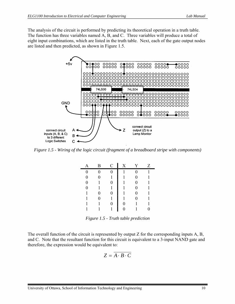
The analysis of the circuit is performed by predicting its theoretical operation in a truth table. The function has three variables named A, B, and C. Three variables will produce a total of eight input combinations, which are listed in the truth table. Next, each of the gate output nodes are listed and then predicted, as shown in Figure 1.5.
Figure 1.5 - Wiring of the logic circuit (fragment of a breadboard stripe with components)
A B C X Y Z 0 0 0 1 0 1 0 0 1 1 0 1 0 1 0 1 0 1 0 1 1 1 0 1 1 0 0 1 0 1 1 0 1 1 0 1 1 1 0 0 1 1 1 1 1 0 1 0
Figure 1.5 - Truth table prediction
The overall function of the circuit is represented by output Z for the corresponding inputs A, B, and C. Note that the resultant function for this circuit is equivalent to a 3-input NAND gate and therefore, the expression would be equivalent to:
CBAZ ⋅⋅=
University of Ottawa, School of Information Technology and Engineering 10
ELG1100 Introduction to Electrical and Computer Engineering Lab Manual
Lab 1 Logic Gates OBJECTIVES:
• To construct simple combinational logic circuits from a schematic. • To test simple combinational logic circuits to determine the functional operation of the
circuits. • To identify common logic functions produced by various circuit configurations by the
resulting truth table. • To connect various gates together to create simple logic functions. • To analyze combinational logic circuits and predict their operation. • To construct and test more complex, combinational logic circuits.
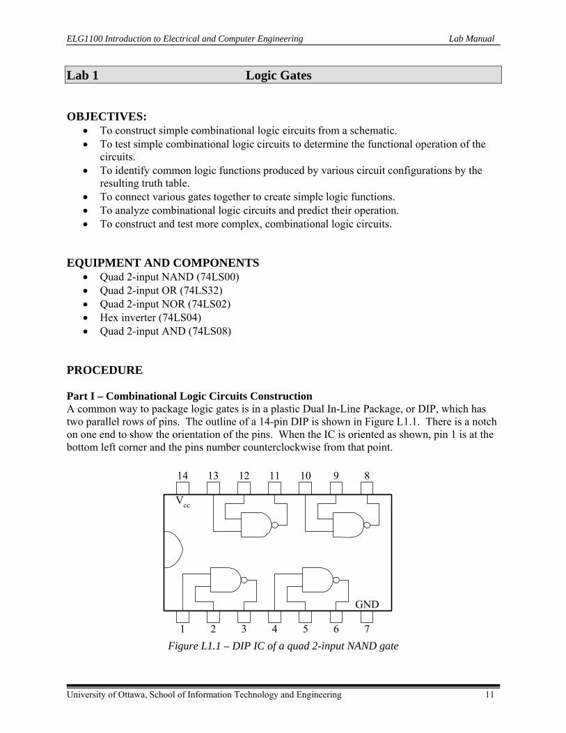
EQUIPMENT AND COMPONENTS • Quad 2-input NAND (74LS00) • Quad 2-input OR (74LS32) • Quad 2-input NOR (74LS02) • Hex inverter (74LS04) • Quad 2-input AND (74LS08)
PROCEDURE Part I – Combinational Logic Circuits Construction A common way to package logic gates is in a plastic Dual In-Line Package, or DIP, which has two parallel rows of pins. The outline of a 14-pin DIP is shown in Figure L1.1. There is a notch on one end to show the orientation of the pins. When the IC is oriented as shown, pin 1 is at the bottom left corner and the pins number counterclockwise from that point.
1213 11
1 2 3
9 810
654 7
14
Vcc
GND
Figure L1.1 – DIP IC of a quad 2-input NAND gate
University of Ottawa, School of Information Technology and Engineering 11

ELG1100 Introduction to Electrical and Computer Engineering Lab Manual
In addition to the gate inputs and outputs, there are two more connections to be made on each chip: the power and ground connections. VCC (pin 14) must be connected to +5 volts and GND (pin 7) to ground to provide power supply connections. The gates won’t work without these connections. Logic levels at the other pin inputs are derived from their power supply voltages by connecting them to + 5 volts for logic 1 and ground for logic 0. You can use the same +5V source to power up both your breadboard and your switch box. If you use different +5V power supplies, make sure you link together their 0V terminals to a common ground. Consult the data sheets at the end of the textbook to see the internal diagrams of the various gates used throughout this laboratory. For each of the following circuits:
1. Write the logic expression. 2. Write the logic truth table. 3. Add on the logic diagram both the codes of the integrated circuits and the pin-out of the
corresponding used gates (see example of Figure 1.4). Build the circuit. 4. Experimentally find out the truth table of the logic function that is implemented by your
built circuit; use each combination of the input logic variables from the truth table as the inputs to your circuit. Verify that the actual output of the circuit matches the corresponding output from the truth table you have theoretically derived (at step 2.).
A. One-chip logic circuit
AB
C R
Figure L1.2 - One- chip logic circuit B. Two-chip logic circuit
ABCD
U
Figure L1.3 - Two-chip logic circuit
University of Ottawa, School of Information Technology and Engineering 12
ELG1100 Introduction to Electrical and Computer Engineering Lab Manual
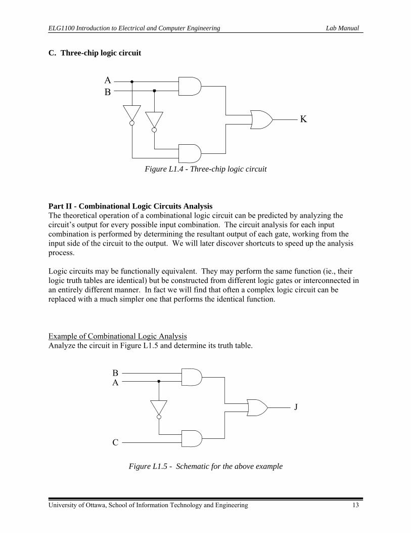
C. Three-chip logic circuit
A
K
B
Figure L1.4 - Three-chip logic circuit
Part II - Combinational Logic Circuits Analysis The theoretical operation of a combinational logic circuit can be predicted by analyzing the circuit’s output for every possible input combination. The circuit analysis for each input combination is performed by determining the resultant output of each gate, working from the input side of the circuit to the output. We will later discover shortcuts to speed up the analysis process.
Logic circuits may be functionally equivalent. They may perform the same function (ie., their logic truth tables are identical) but be constructed from different logic gates or interconnected in an entirely different manner. In fact we will find that often a complex logic circuit can be replaced with a much simpler one that performs the identical function. Example of Combinational Logic AnalysisAnalyze the circuit in Figure L1.5 and determine its truth table.
A
J
B
C
Figure L1.5 - Schematic for the above example
University of Ottawa, School of Information Technology and Engineering 13
ELG1100 Introduction to Electrical and Computer Engineering Lab Manual
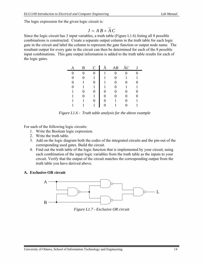
The logic expression for the given logic circuit is:
CABAJ += Since the logic circuit has 3 input variables, a truth table (Figure L1.6) listing all 8 possible combinations is constructed. Create a separate output column in the truth table for each logic gate in the circuit and label the column to represent the gate function or output node name. The resultant output for every gate in the circuit can then be determined for each of the 8 possible input combinations. This gate output information is added to the truth table results for each of the logic gates.
A B C Ā AB ĀC J 0 0 0 1 0 0 0 0 0 1 1 0 1 1 0 1 0 1 0 0 0 0 1 1 1 0 1 1 1 0 0 0 0 0 0 1 0 1 0 0 0 0 1 1 0 0 1 0 1 1 1 1 0 1 0 1
Figure L1.6 - Truth table analysis for the above example
For each of the following logic circuits:
1. Write the Boolean logic expression. 2. Write the truth table. 3. Add on the logic diagram both the codes of the integrated circuits and the pin-out of the
corresponding used gates. Build the circuit. 4. Find out the truth table of the logic function that is implemented by your circuit, using
each combination of the input logic variables from the truth table as the inputs to your circuit. Verify that the output of the circuit matches the corresponding output from the truth table you have derived above.
A. Exclusive-OR circuit
L
A
B
Figure L1.7 - Exclusive OR circuit
University of Ottawa, School of Information Technology and Engineering 14
ELG1100 Introduction to Electrical and Computer Engineering Lab Manual
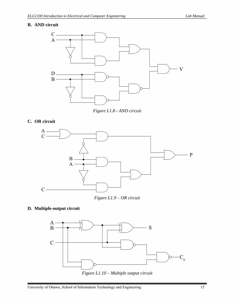
B. AND circuit
CA
DB
V
Figure L1.8 - AND circuit
C. OR circuit
A
P
C
C
BA
Figure L1.9 – OR circuit
D. Multiple-output circuit
SAB
C
Co
Figure L1.10 – Multiple output circuit
University of Ottawa, School of Information Technology and Engineering 15

ELG1100 Introduction to Electrical and Computer Engineering Lab Manual
Lab 2 Boolean Logic OBJECTIVES:
• To simplify logic functions starting from their logic truth tables or Boolean expressions • To synthesize, implement and test minimized combinational circuits. • To devise and design combinational logic circuits from specifications. • To implement combinational circuits using any type of available logic gates. • To implement combinational circuits using NAND gates only.
EQUIPMENT AND COMPONENTS
• Quad 2-input NAND (74LS00) • Quad 2-input AND (74LS08) • Triple 3-input NAND (74LS10) • Quad 2-input OR (74LS32) • Quad 2-input NOR (74LS02) • Quad 2-input XOR (74LS86) • Hex inverter (74LS04)
PROCEDURE Part I – Combinational Logic Circuits minimization by Boolean Algebra
A logic function is given by the following Boolean expression:
BADCBADCBAY +++⋅++⋅⋅⋅= )()( (1)
1. Draw the logic circuit that implements this logic function. 2. Derive the truth table of Y as a function of logic variables A, B, C and D. 3. Use the rules of Boolean algebra to simplify expression (1) as much as possible. 4. Draw the logic circuit that implements this minimized function. Write on it both the
codes of the integrated circuits and the pin-out of the corresponding used gates. 5. Build the minimized logic circuit on your breadboard. 6. Find experimentally the truth table of your circuit by applying each combination of
the logic variables A, B, C and D to its inputs. Verify that the output of the minimized circuit matches the corresponding output from the truth table you initially found.
University of Ottawa, School of Information Technology and Engineering 16

ELG1100 Introduction to Electrical and Computer Engineering Lab Manual
Part II – Combinational Logic Circuits minimization by the Karnaugh Map Method
A logic function is given by the following truth table
A B C D Y 0 0 0 0 0 1 1 0 0 0 1 0 2 0 0 1 0 1 3 0 0 1 1 0 4 0 1 0 0 0 5 0 1 0 1 0 6 0 1 1 0 0 7 0 1 1 1 0 8 1 0 0 0 1 9 1 0 0 1 1
10 1 0 1 0 1 11 1 0 1 1 1 12 1 1 0 0 0 13 1 1 0 1 0 14 1 1 1 0 1 15 1 1 1 1 0
1. Derive the canonic sum-of-products (SOP) expression of the function Y(A, B, C, D)
from the above truth table. 2. Use the Karnaugh map method to reduce this canonic SOP expression to the simplest
SOP form.
CD 00 01 11 10 AB
00 0 1 3 2
Y
01 4 5 7 6
11 12 13 15 14
10 8 9 11 10
3. Draw the logic diagram of the SOP minimized circuit. 4. Use the De Morgan’s theorems to express the simplest SOP in terms of NAND
operators; implement this expression using NAND gates only. Draw the logic diagram of this circuit (specifying the pin-out of the component gates) and built it on your breadboard.
University of Ottawa, School of Information Technology and Engineering 17

ELG1100 Introduction to Electrical and Computer Engineering Lab Manual
5. Find out the truth table of the minimized circuit that you have built with NAND gates, by applying each combination of the logic variables A, B, C and D to its inputs. Verify that its output matches the corresponding output from the given truth table.
6. Use the Karnaugh map method to find the simplest product-of-sums (POS) expression of the function Y(A, B, C, D).
7. Draw the logic diagram of the circuit that implements the POS minimized expression. Analyze the circuit that implements the POS minimized expression and determine its truth table
8. Show that your POS minimized circuit is equivalent with the previous one that implemented the simplest SOP form.
Part III – Design of Combinational Logic Circuits
4 bit numbers (N) are presented to the inputs (D3, D2, D1, D0), of the logic circuit from the block diagram of figure L2.1. D3 is the most significant bit (msb) of the binary representation of N, while D0 is the least significant bit (lsb). The output (P) of this circuit has to be HIGH if the current input number N is prime and LOW if that number is divisible.
Logic circuit
D3
D2
D1
D0
P
Figure L2.1 – Block diagram of a prime number detector
1. Devise and write down the truth table of P as a function of logic variables D3, D2, D1 and D0.
N D3 D2 D1 D0 P 0 0 0 0 0 1 0 0 0 1 2 0 0 1 0 3 0 0 1 1 4 0 1 0 0 5 0 1 0 1 6 0 1 1 0 7 0 1 1 1 8 1 0 0 0 9 1 0 0 1
10 1 0 1 0 11 1 0 1 1 12 1 1 0 0 13 1 1 0 1 14 1 1 1 0 15 1 1 1 1
University of Ottawa, School of Information Technology and Engineering 18

ELG1100 Introduction to Electrical and Computer Engineering Lab Manual
2. Derive the canonical sum-of-products (SOP) expression of the function P(D3, D2, D1,
D0) from its truth table. 3. Use the Karnaugh map method to reduce this canonical SOP expression to the
simplest SOP form. 4. Use the De Morgan’s theorems to express the simplest SOP in terms of NAND
operators; implement this expression using NAND gates only. Draw the logic diagram of this circuit and built it on your breadboard.
5. Find experimentally the truth table of your circuit by applying to its inputs all numbers from 0 to 15 in binary form. Verify that the output of the minimized circuit matches the corresponding output from the truth table you initially devised.
6. Using Boolean algebra, try to minimize further the simplest SOP, at the expense of increasing the number of levels of logic gates.
7. Draw the logic diagram of the circuit that implements the last minimized expression and built it on your breadboard.
8. Show that your minimized circuit is equivalent with the previous one that implemented the simplest SOP form, by verifying experimentally that they have identical truth tables.
University of Ottawa, School of Information Technology and Engineering 19
ELG1100 Introduction to Electrical and Computer Engineering Lab Manual
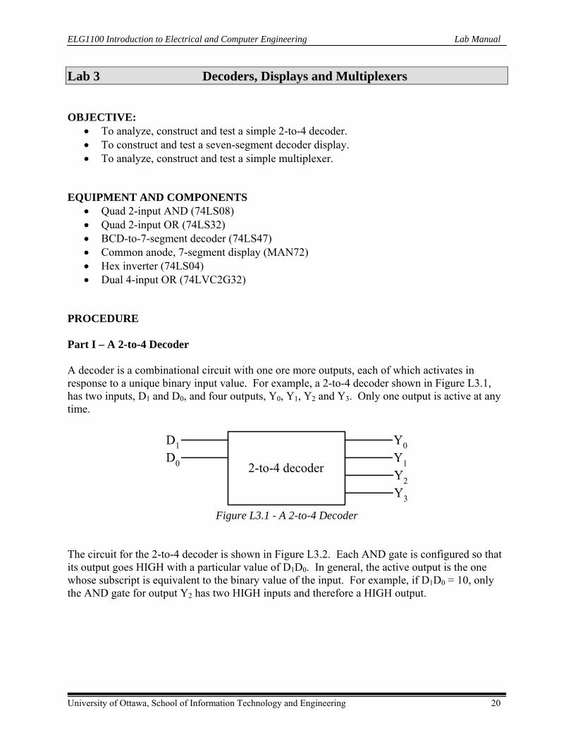
Lab 3 Decoders, Displays and Multiplexers OBJECTIVE:
• To analyze, construct and test a simple 2-to-4 decoder. • To construct and test a seven-segment decoder display. • To analyze, construct and test a simple multiplexer.
EQUIPMENT AND COMPONENTS
• Quad 2-input AND (74LS08) • Quad 2-input OR (74LS32) • BCD-to-7-segment decoder (74LS47) • Common anode, 7-segment display (MAN72) • Hex inverter (74LS04) • Dual 4-input OR (74LVC2G32)
PROCEDURE Part I – A 2-to-4 Decoder A decoder is a combinational circuit with one ore more outputs, each of which activates in response to a unique binary input value. For example, a 2-to-4 decoder shown in Figure L3.1, has two inputs, D1 and D0, and four outputs, Y0, Y1, Y2 and Y3. Only one output is active at any time.
2-to-4 decoder
D1D0
Y0Y1Y2Y3
Figure L3.1 - A 2-to-4 Decoder The circuit for the 2-to-4 decoder is shown in Figure L3.2. Each AND gate is configured so that its output goes HIGH with a particular value of D1D0. In general, the active output is the one whose subscript is equivalent to the binary value of the input. For example, if D1D0 = 10, only the AND gate for output Y2 has two HIGH inputs and therefore a HIGH output.
University of Ottawa, School of Information Technology and Engineering 20
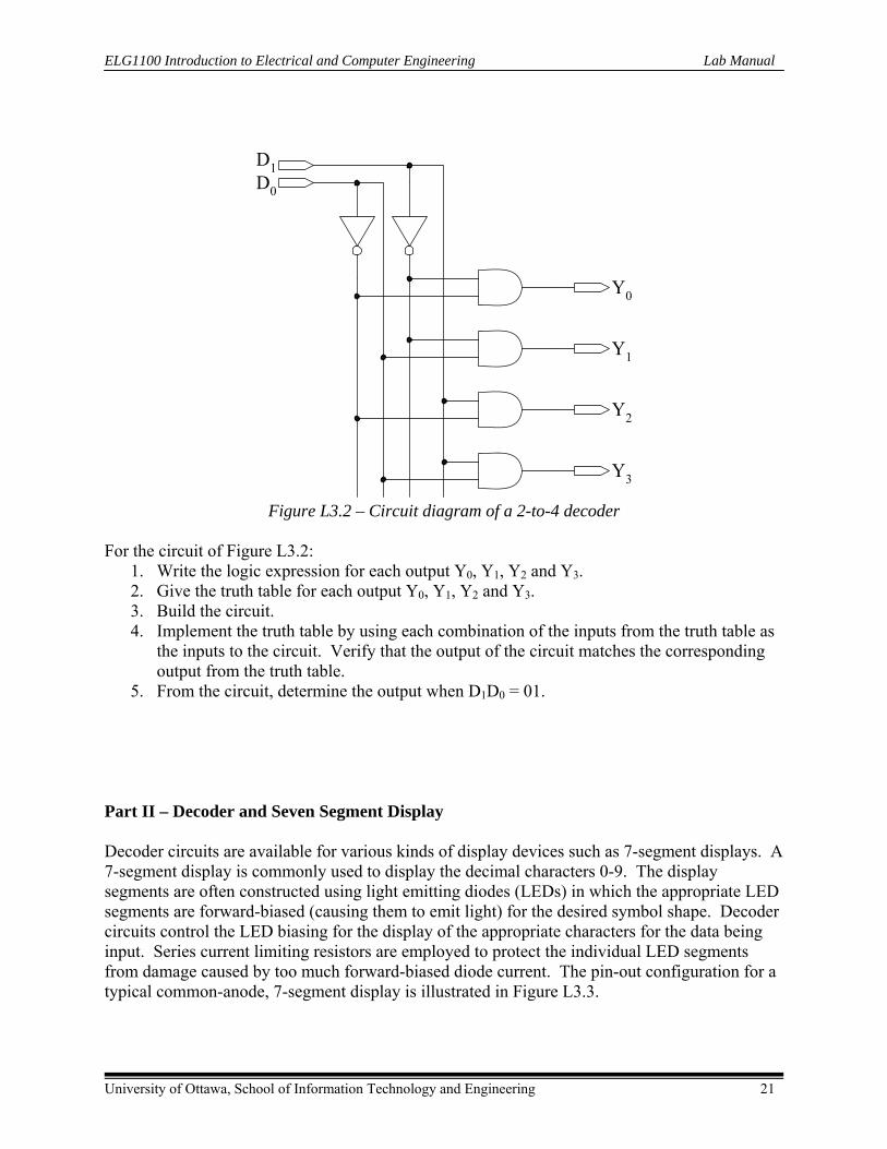
ELG1100 Introduction to Electrical and Computer Engineering Lab Manual
Y0
Y1
Y2
Y3
D1D0
Figure L3.2 – Circuit diagram of a 2-to-4 decoder
For the circuit of Figure L3.2:
1. Write the logic expression for each output Y0, Y1, Y2 and Y3. 2. Give the truth table for each output Y0, Y1, Y2 and Y3. 3. Build the circuit. 4. Implement the truth table by using each combination of the inputs from the truth table as
the inputs to the circuit. Verify that the output of the circuit matches the corresponding output from the truth table.
5. From the circuit, determine the output when D1D0 = 01. Part II – Decoder and Seven Segment Display Decoder circuits are available for various kinds of display devices such as 7-segment displays. A 7-segment display is commonly used to display the decimal characters 0-9. The display segments are often constructed using light emitting diodes (LEDs) in which the appropriate LED segments are forward-biased (causing them to emit light) for the desired symbol shape. Decoder circuits control the LED biasing for the display of the appropriate characters for the data being input. Series current limiting resistors are employed to protect the individual LED segments from damage caused by too much forward-biased diode current. The pin-out configuration for a typical common-anode, 7-segment display is illustrated in Figure L3.3.
University of Ottawa, School of Information Technology and Engineering 21
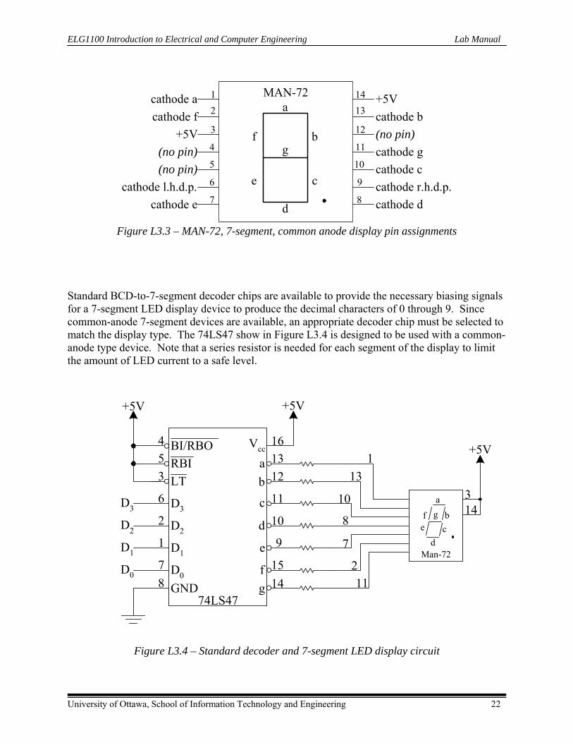
ELG1100 Introduction to Electrical and Computer Engineering Lab Manual
MAN-72a
g
d
bf
ce
cathode acathode f
+5V(no pin)(no pin)
cathode l.h.d.p.cathode e
+5Vcathode b(no pin)cathode gcathode ccathode r.h.d.p.cathode d
12
3
4
5
6
7
1413
12
11
10
9
8
Figure L3.3 – MAN-72, 7-segment, common anode display pin assignments
Standard BCD-to-7-segment decoder chips are available to provide the necessary biasing signals for a 7-segment LED display device to produce the decimal characters of 0 through 9. Since common-anode 7-segment devices are available, an appropriate decoder chip must be selected to match the display type. The 74LS47 show in Figure L3.4 is designed to be used with a common-anode type device. Note that a series resistor is needed for each segment of the display to limit the amount of LED current to a safe level.
D3
D2
D1
D0
LTRBIBI/RBO Vcc
ab
c
d
e
fgGND
453
6
2
1
78
161312
11
10
9
1514
113
10
8
7
211
314D3
D2
D1
D0
+5V +5V
+5V
74LS47
e
a
bc
d
f g
Man-72
Figure L3.4 – Standard decoder and 7-segment LED display circuit
University of Ottawa, School of Information Technology and Engineering 22
ELG1100 Introduction to Electrical and Computer Engineering Lab Manual
For the circuit in Figure L3.4:
1. Build the circuit. 2. Complete the table below with the display that the 7-segment LED produces for the given
inputs of D3D2D1D0. 3. Verify that the corresponding display is correct by comparing it to the truth table given in
your textbook on page 174.
D3D2D1D0 Corresponding Display
D3D2D1D0 Corresponding Display
0000 0001
0010 0011
0100 0101
0110 0111
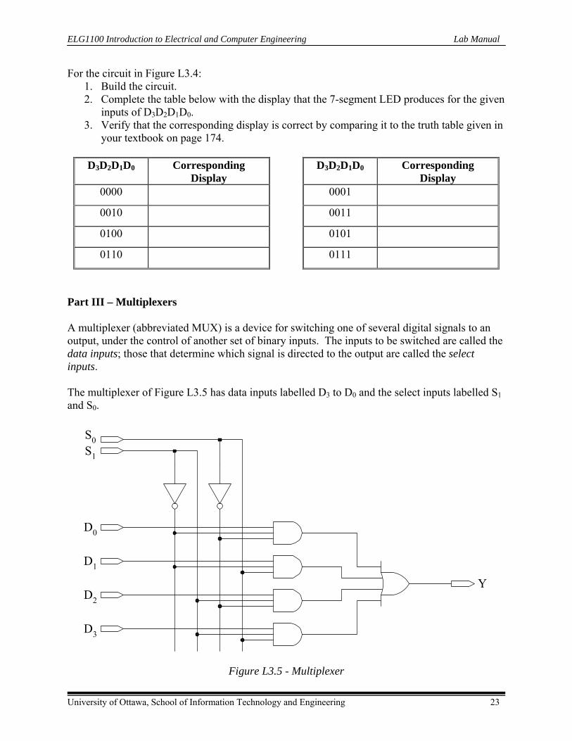
Part III – Multiplexers A multiplexer (abbreviated MUX) is a device for switching one of several digital signals to an output, under the control of another set of binary inputs. The inputs to be switched are called the data inputs; those that determine which signal is directed to the output are called the select inputs. The multiplexer of Figure L3.5 has data inputs labelled D3 to D0 and the select inputs labelled S1 and S0.
S0S1
D0
D1
D2
D3
Y
Figure L3.5 - Multiplexer
University of Ottawa, School of Information Technology and Engineering 23

ELG1100 Introduction to Electrical and Computer Engineering Lab Manual
For the circuit in Figure L3.5:
1. Determine the kind of multiplexer the circuit represents (i.e. Is it a 2-1 MUX or a 4-1 MUX?).
2. Write the Boolean expression that describes this MUX. 3. From the Boolean expression, determine what Y is when S1S0 = 01. 4. Determine the truth table with S1 and S0 as the selection inputs, D0, D1, D2 and D3 as the
data inputs and Y as the output. 5. Build the circuit. 6. Implement the truth table by using each combination of the inputs from the truth table as
the inputs to the circuit. Verify that the output of the circuit matches the corresponding output from the truth table.
University of Ottawa, School of Information Technology and Engineering 24

ELG1100 Introduction to Electrical and Computer Engineering Lab Manual
Lab 4 Arithmetic Circuits
OBJECTIVE:
• Create and simulate a full adder, assign pins to the design, and test it on the Altera UP-1 CPLD circuit board.
• Use a full adder as a component in an 8-bit adder/subtractor. • Create a hierarchical design, including components for full adders and seven-segment
decoders, using the QUARTUS II graphic editor. • Design an overflow detector for use in a two’s complement adder/subtractor.
EQUIPMENT AND COMPONENTS
• QUARTUS II Student Edition Software • Altera UP-1 CPLD circuit board • AC adapter, minimum output: &VDC, 250mA DC • Anti-static wrist straps • #22 solid-core wires • Wire strippers
Note: You are required to go over and practice “Short Tutorial on Altera Quartus II” appendix presented at the end of this manual before you attempt this laboratory experiment. DOWNLOADING AND INSTALLING QUARTUS II (AT HOME, LAPTOP) Download: The web edition of the software can be downloaded from Altera website at the following link: https://www.altera.com/support/software/download/altera_design/quartus_we/dnl-quartus_we.jsp Installation: Instructions to install the software are given at the following link: https://www.altera.com/support/software/download/altera_design/quartus_we/ins-webdnl_consol.html Setting up licensing: In order to run the web edition of the Quartus II you need to obtain free academic license, this can be obtained from the following link: https://www.altera.com/support/software/download/ins-license.html
University of Ottawa, School of Information Technology and Engineering 25

ELG1100 Introduction to Electrical and Computer Engineering Lab Manual
EXPERIMENTAL NOTES Arithmetic Circuits Circuits for performing binary arithmetic are based on half adders, which add two bits and produce a sum and carry, and full adders, which also account for a carry added from the lesser-significant bit. Full adders can be grouped together to make a parallel binary adder, with n full adders allowing two n-bit numbers to be added, generating an n-bit sum and a carry output. A parallel adder can be converted to a two’s complement adder/subtractor by including XOR functions on the inputs of one set of operand bits, say input B, allowing the operations A + B or A - B to be performed. A control input, SUB (for SUBtract), causes XORs to invert the B bits if HIGH, producing the one’s complement of B. SUB will not invert B if LOW, transferring B to the parallel adder without modification. If SUB is also tied to the carry input of the parallel adder, the result is (A + B + 0 = A + B) when SUB = 0 and ( BABA −=++ 1 ) when SUB = 1, where B is the one’s complement of B and ( B + 1) is its two’s complement. Sign-bit overflow occurs when a two’s complement sum of difference exceeds the permissible range of numbers for a given bit size. This can be detected by an SOP circuit that compares the operands and result sign bits of a parallel adder if the 2’s complement is used to represent the. PROCEDURE Part I – Full Adders
1. The logic diagram for a full adder is shown in Figure L4.1. Use the QUARTUS II graphic editor to capture this logic diagram into a Block Diagram/Schematic File (name it F_Adder.bdf). Compile the project. Assign pin numbers to the design, as shown in Figure L4.2.
AB
C_IN
C_OUT
SUM
Figure L4.1 – Full adder circuit
Function Device Pin A SW1-1 34 B SW1-2 33
C_IN SW1-3 36 C_OUT LED1 44
SUM LED2 45
University of Ottawa, School of Information Technology and Engineering 26

ELG1100 Introduction to Electrical and Computer Engineering Lab Manual
Figure L4.2 – Pin assignments for a full adder 2. Compile the file. 3. Create and run a simulation for the full adder and show it to your instructor. 4. Download the full adder design to your CPLD board. Invert the inputs and outputs of the
full adder to make them active-LOW. Take the truth table of the full adder to verify its operation. Show the results to your instructor.
NOTE: The Switches, LEDs on the Altera UP-1 are active-LOW (illuminated by logic 0 and represent 0 when pressed respectively). To transform these devices into active-HIGH devices you have to connect them to your circuit through 5 not inverters. Notice that these invertors should not be used during simulation.
Part II – Parallel Adder
1. Create an 8-bit parallel adder using the previous full adder in your graphic editor. From main menu go to: File>create-Update>Create Symbol File for Current file Open a new Block Diagram/Schematic File double click on the empty Schematic file and from the libraries under Project insert F_Adder symbol. Repeat this process 8 times to create 8 different instances of you One Bit Full Adder.
2. Save this file as TopLevel.bdf. 3. Inside Project Navigator window click on Files Tab, right click on TopLevel.bdf and
Set As Top-Level Entry. 4. Connect all the inputs and outputs. Make sure that the inputs and outputs of the full adder
component are active-HIGH (no not gate), even if you used active-LOW inputs and outputs in the previous section to use with switches and LEDs. Make sure that the switche inputs , sum and carry outputs of the parallel adder are active-LOW (i.e., inverted) to display them properly on the Altera-UP1 board LEDs.
NOTE: The circuit outputs can be inverted either with inverters or by using the Edit Ports/Parameters function of the QUARTUS II graphic editor, as follows. Click on one of the F_Adder symbol in TopLevel.bdf to highlight it, then right-click to get the pop-up menu. Select Properties; then go to Ports Tab, dialog box will appear. Select the output you want to modify from the Name box and check All in the inversion box. Do not click OK just yet, but rather select another output you want to change and invert it. Click OK after you finished.
5. Follow the examples shown below to add the unsigned binary numbers in Figure L4.3, giving the sum in both binary and hexadecimal. Show the carry output separately. e.g.: 10111111 + 10000001 = 01000000 (Carry output = 1); Hexadecimal equivalent: BFH + 81H = 40H (Carry output = 1) e.g.: 00111111 + 0000001 = 01000000 (Carry output = 0) Hexadecimal equivalent: 3FH + 01H = 40H (Carry output = 0)
Binary Inputs Carry Binary Sum Hex Equivalent 01111111 + 00000001
11111111 + 00000001
11000000 + 01000000
11000000 + 10000000
University of Ottawa, School of Information Technology and Engineering 27

ELG1100 Introduction to Electrical and Computer Engineering Lab Manual
Figure L4.3 – Sample Sums for an 8-bit Parallel Adder
6. Use the sums calculated in Figure L4.3 to create a simulation of the 8-bit parallel adder. The sums in the simulation must match those in Figure L4.3. Show the simulation to your instructor.
7. Assign pins to the 8-bit adder as shown in Figure L4.4. Wire up the circuit inputs to 16 onboard DIP switches (A0-A7, B0-B7) and C_IN to a Pushbutton. Wire up the circuit outputs (S0-S7 and C_OUT) to 9 onboard LEDs.
8. Compile the file and download the design for the 8-bit parallel adder to your CPLD board. Test the operation of the 8-bit parallel adder by applying the combinations of inputs A and B listed in Figure L4.4. Show the results to your instructor.
Figure L4.4 – Pin assignments for an 8-bit Parallel Adder
Part III – Two’s Complement Adder/Subtractor (Optional)
1. Modify the 8-bit adder you created to make an 8-bit two’s complement adder/subtractor. Include an overflow detector that will turn on a LED when the output of the adder/ subtractor overflows beyond the permissible range of the values for an 8-bit (2’s complement) signed number. Display the sum outputs on LEDs, as with the previous 8-bit adder from Part II.
University of Ottawa, School of Information Technology and Engineering 28

ELG1100 Introduction to Electrical and Computer Engineering Lab Manual
2. Follow the examples shown to add the signed binary numbers in Figure L4.5, giving the sum in both binary and hexadecimal. Show the carry and overflow outputs separately from the sum. (Note that the CARRY OUTPUT is not used for signed additions and subtractions. However, we retain the function so that the same circuit can be used for both signed and unsigned arithmetic.)
e.g.: 01111111 + 01000001 = 11000000 (Overflow = 1, Carry output = 0); Hexadecimal equivalent: 7FH + 41H = C0H
e.g.: 00000000 - 00000011 = 11111101 (Overflow = 0, Carry output = 0); Hexadecimal equivalent: 00H – 03H = FDH (two’s complement: FDH = 11111101 = (-310))
Binary Inputs Overflow Carry Binary Sum Hex Equivalent Two’s Compl.
01111111 + 00000001
11111111 + 00000001
00000000 - 00000001
00000000 - 01111111
11000000 + 01000000
11000000 + 10000000
Figure L4.5 – Sample sums and differences for an 8-bit adder/subtractor
3. Leave the pin assignments and wiring the same as for the 8-bit adder, except for Add/Sub input which will be tied to a the second onboard Pushbutton and port 11 and overflow output which will be tied to a free LED through port 51.
4. Compile the file and download it to the CPLD board. Test the operation of the circuit by
applying the A and B inputs from Figure L4.5. Show the results to your instructor.
University of Ottawa, School of Information Technology and Engineering 29

ELG1100 Introduction to Electrical and Computer Engineering Lab Manual
Lab 5 Latches and Flip-Flops OBJECTIVES: • To provide insight into the characteristics of several important latches and flip-flops. • To build latches and flip-flops from basic gates. • To explain concepts of latching and edge-triggering. • To test latches and flip-flops to understand their operation EQUIPMENT AND COMPONENTS
• Quad 2-input NAND (74LS00) • Quad 2-input AND (74LS08) • Hex inverter (74LS04) • Quad positive-edge triggered D flip-flops (74LS175)
A sequential circuit is a digital circuit whose output depends not only on the present combination of input, but also on the history of the circuit. A sequential circuit element is a basic memory element that can store 1 bit. There are two basic types of sequential circuit elements: the latch and the flip-flop. The difference is the condition under which the stored bit changes. PROCEDURE Part I – SR Latch The simplest sequential circuit element is the SR latch. It presents two asynchronous inputs (SET –that makes the device store a logic 1 and RESET – an input that makes the device store a logic 0) and two complementary outputs, Q and Q that are always in opposite logic states (Fig. L5.1)
Figure L 5.1 SR latch
The SR latch presents two stable states: SET or ON when Q = 1 and Q = 0. RESET or OFF when Q = 0 and Q = 1.
University of Ottawa, School of Information Technology and Engineering 30
ELG1100 Introduction to Electrical and Computer Engineering Lab Manual
The four possible input combinations will generate the following actions of the latch:
S R Action 0 0 Output does not change from the previous state 0 1 RESET 1 0 SET 1 1 Forbidden condition: it doesn’t make any sense
to ask to store at the same time both 0 and 1!!!!!!
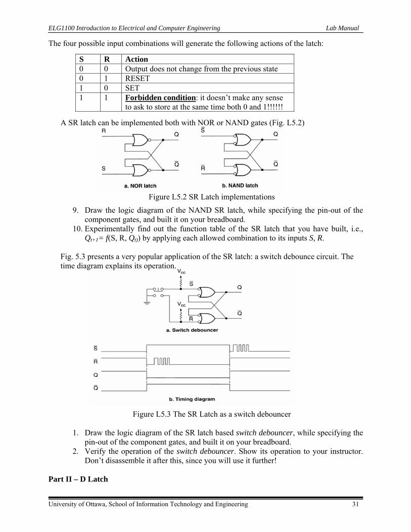
A SR latch can be implemented both with NOR or NAND gates (Fig. L5.2)
Figure L5.2 SR Latch implementations
9. Draw the logic diagram of the NAND SR latch, while specifying the pin-out of the component gates, and built it on your breadboard.
10. Experimentally find out the function table of the SR latch that you have built, i.e., Q = f(S, R, Qt+1 t)) by applying each allowed combination to its inputs S, R.
Fig. 5.3 presents a very popular application of the SR latch: a switch debounce circuit. The time diagram explains its operation.
Figure L5.3 The SR Latch as a switch debouncer
1. Draw the logic diagram of the SR latch based switch debouncer, while specifying the pin-out of the component gates, and built it on your breadboard.
2. Verify the operation of the switch debouncer. Show its operation to your instructor. Don’t disassemble it after this, since you will use it further!
Part II – D Latch
University of Ottawa, School of Information Technology and Engineering 31

ELG1100 Introduction to Electrical and Computer Engineering Lab Manual
The forbidden state is eliminated in the D latch (Fig. L5.4). This latch has two operating modes that are controlled by the ENABLE input (EN): when the EN is active, the latch output follows the data input (D) and when EN is inactive, the latch stores the data that was present when EN was last active.
D
•
•
•
•
EN
Q
Q
S R
Figure L 5.4. (Transparent) D latch The D latch behaviour is presented in the following function table: EN D Q Action Comment
1+tQ t+1
0 x Q Output does not change from the previous state Store tQ t
1 0 0 1 RESET Transparent 1 1 1 0 SET
1. Draw the logic diagram of the NAND D latch, while specifying the pin-out of
component gates, and built it on your breadboard. 2. Use the switch debouncer to generate the EN input. Find out the function table of the
D latch that you have built, and compare it with the one given above. 3. Experimentally show that the latch output follows the D input when EN is HIGH, but
doesn’t change with D as the EN is LOW. Show to your instructor. Part III – D Flip-Flop A Flip-Flop is a gated latch with a clock input. The flip-flop output changes when its CLOCK input (CLK) detects an edge. This sequential circuit element is edge-sensitive (and not level-sensitive, as the latch). Figure L5.5 presents the symbols for a Positive-Edge Triggered D Flip-Flop and a Negative-Edge Triggered D Flip-Flop.
D Q CLK Q
D Q CLK Q
Fig L5.5 Positive-Edge Triggered D Flip-Flop and Negative-Edge Triggered D Flip-Flop
The following table presents the operation of a Positive-Edge Triggered D Flip-Flop. It shows that the D input is sampled during the positive edge of the clock signal (CLK) and it is stored in the D Flip-Flop and presented to its output. Any other changes that may occur at the both CLK
University of Ottawa, School of Information Technology and Engineering 32

ELG1100 Introduction to Electrical and Computer Engineering Lab Manual
and D inputs, while the CLK input is stable (at 0 or 1) or it is down going, will have no effect to the flip-flop state and its output.
CLK D Q Function 1+tQ t+1
↑ 0 0 1 RESET ↑ 1 1 0 SET 0 X Q Inhibited
tQ t
1 X Q Inhibited tQ t
The following experiment will be performed on one of the four positive-edge triggered D flip-flops with common CLOCK and common RESET from the TTL IC 74175 (Fig.L5.6)
+----------+ +-----------------------+ RST |1 +--+ 16| VCC | RST| CLK| D | Q |Q | t+1 t+1
Q1 |2 15| Q4 |----+----+---+-----+---| /Q1 |3 14| /Q4 | 0 | X | X | 0 | 1 | D1 |4 74 13| D4 | 1 | | | 0 | 0 | 1 | D2 |5 175 12| D3 | 1 | | | 1 | 1 | 0 | /Q2 |6 11| /Q3 | 1 |no| | X | Q | Q | t t
Q2 |7 10| Q3 +-----------------------+ GND | | CLK 8 9 +----------+
Fig. L5.6 74175 pin-out and function table
1. Draw the block diagram of the positive-edge triggered D flip-flop from 74715 with
the CLK generated by the switch debouncer you have built in part I.; specify the pin-out of the used components, and build this circuit on your breadboard.
2. Experimentally determine on which edge of the CLK signal triggering occurs. Note in your lab report the procedures you have used.
3. Experimentally find out the function table of the positive-edge triggered D flip-flop that you have built, and compare it with the one given above.
Part IV – T Flip-Flop A T Flip-Flop is a flip-flop whose output toggles between HIGH and LOW on each clock pulse when input T is active.
1. Design a T flip-flop based on a positive-edge triggered D flip-flop. Draw its logic diagram, while specifying the pin-out of the used components. Built the T flip-flop on your breadboard.
2. Experimentally find out the function table of the built T flip-flop.
University of Ottawa, School of Information Technology and Engineering 33

ELG1100 Introduction to Electrical and Computer Engineering Lab Manual
Lab 6 Synchronous Counters
OBJECTIVES: Upon completion of this laboratory exercise, you should be able to:
• Design synchronous counters; enter the design using the QUARTUS II graphic editor. • Simulate the functions of the various counters in this laboratory exercise. • Assign pins to the designs; download them into the EPM7128S CPLD of the Altera UP-1
circuit board. • Display counters outputs as binary values on LEDs and test these counters.
EQUIPMENT AND COMPONENTS
• Altera UP-1 Circuit Board with ByteBlaster Download Cable and Altera EPM7128S CPLD
• QUARTUS II Student Edition Software • AC adapter, minimum output: &VDC, 250mA DC • Anti-static wrist straps • #22 solid-core wire • Wire strippers
DESIGN NOTES The count sequence is the starting point in the design of synchronous counters; it can be specified by a table or a state diagram. In the following example will illustrate the design process of a synchronous counter with the count sequence given by the state diagram of figure L6.1.
11110001
0000 1000 1100 1101
0011 0010 0110 1110
Reset
Figure L6.1 Since the state codes are represented by 4 bits, there are required 4 flip-flops to implement the synchronous counter. Based on this state diagram, the counter’s state table is derived: the first 2 groups (each of 4 columns) of Figure L6.2 describe the present and the next state of the counter’s 4 flip-flops (Q3, Q , Q , Q ). 2 1 0 While synchronous counters can be designed using any type of flip-flop, JK and D flip-flops are commonly used for this function; our example is making use of JK flip-flops. The corresponding JK inputs are derived for every transition from the excitation table of the JK flip-flop.
University of Ottawa, School of Information Technology and Engineering 34
ELG1100 Introduction to Electrical and Computer Engineering Lab Manual
University of Ottawa, School of Information Technology and Engineering 35
Present state(n) Next state(n+1) Q3 input Q2 input Q1 input Q0 input
Q3 Q2 Q1 Q0 Q3 Q2 Q1 Q0 J3 K3 J2 K2 J1 K1 J0 K0
0 0 0 0 1 0 0 0 1 x 0 x 0 x 0 x 0 0 0 1 0 0 0 0 0 x 0 x 0 x x 1 0 0 1 0 0 0 1 1 0 x 0 x x 0 1 x 0 0 1 1 0 0 0 1 0 x 0 x x 1 x 0 0 1 0 0 x x x x x x x x x x x x 0 1 0 1 x x x x x x x x x x x x 0 1 1 0 0 0 1 0 0 x x 1 x 0 0 x 0 1 1 1 x x x x x x x x x x x x 1 0 0 0 1 1 0 0 x 0 1 x 0 x 0 x 1 0 0 1 x x x x x x x x x x x x 1 0 1 0 x x x x x x x x x x x x 1 0 1 1 x x x x x x x x x x x x 1 1 0 0 1 1 0 1 x 0 x 0 0 x 1 x 1 1 0 1 1 1 1 1 x 0 x 0 1 x x 0 1 1 1 0 0 1 1 0 x 1 x 0 x 0 0 x 1 1 1 1 1 1 1 0 x 0 x 0 x 0 x 1
Figure L6.2
The equations of the synchronous inputs are found from the corresponding Karnaugh maps, making use of the don’t care terms of the excitation table (x) and the unused combinations (marked with bold x’s)
Q1Q0 00 01 11 10 Q1Q0 00 01 11 10 Q3Q2 Q3Q2
00 1 0 0 0 00 x x x x 01 x x x 01 x x x x 11 x x x x 11 0 0 0 1 10 x x x x 10 0 x x x
013 QQJ ⋅= 013 QQK ⋅=
Q1Q0 00 01 11 10 Q1Q0 00 01 11 10 Q3Q2 Q3Q2
00 0 0 0 0 00 x x x x 01 x x x x 01 x x x 1 11 x x x x 11 0 0 0 0 10 1 x x x 10 x x x x
32 QJ = 32 QK =
Q1Q0 00 01 11 10 Q1Q0 00 01 11 10

ELG1100 Introduction to Electrical and Computer Engineering Lab Manual
Q Q Q Q 3 2 3 2
00 0 0 x x 00 x x 1 0 x x x 01 x 01 x x x 0
11 0 1 x x 11 x x 0 0 x x x x x x 10 0 10 x
031 QQK ⋅= 031 QQJ ⋅=
Q Q 00 01 11 10 Q Q 00 01 11 10 1 0 1 0Q Q Q Q 3 2 3 2
00 0 x x 1 00 x 1 0 x x x x 01 0 01 x x x x
11 1 x x 0 11 x 0 1 x x x x 10 0 10 x x x x
130 QQK ⊕=120 QQJ ⊕= Based on these equations, the logic diagram of Figure L6.3 is drawn. For more detail, see Section 9.3, pp. 376-384, in Digital Design with CPLD Applications and VHDL. Procedure
4-bit Synchronous Counter 1. Use the QUARTUS II graphic editor to
enter the 4-bit synchronous counter shown in Figure L6.3. Capture the logic diagram from this .bdf file and save it in graphic format (.bmp, .jpeg, .gif, etc…) for your lab report.
2. Compile and simulate your design. 3. Create a Symbol for this counter by
going to File > Create/Update > Create Symbol File for Current File Menu. Now you can use this circuit as a component (sub-circuit) of another circuit to be designed in next steps.
Figure L6.3
University of Ottawa, School of Information Technology and Engineering 36
ELG1100 Introduction to Electrical and Computer Engineering Lab Manual
4. In order to manually clock the counter from procedure 1 with a pushbutton switch, we require a switch debouncer, which is provided in the file debounce.tdf from the C:\max2work\ahdl directory in the computers in laboratory. Copy this file to your working folder (don’t forget to remove its read-only property!), open the file. Create a default symbol for the debouncer as you did in step 3. (Do not worry about understanding how it works)
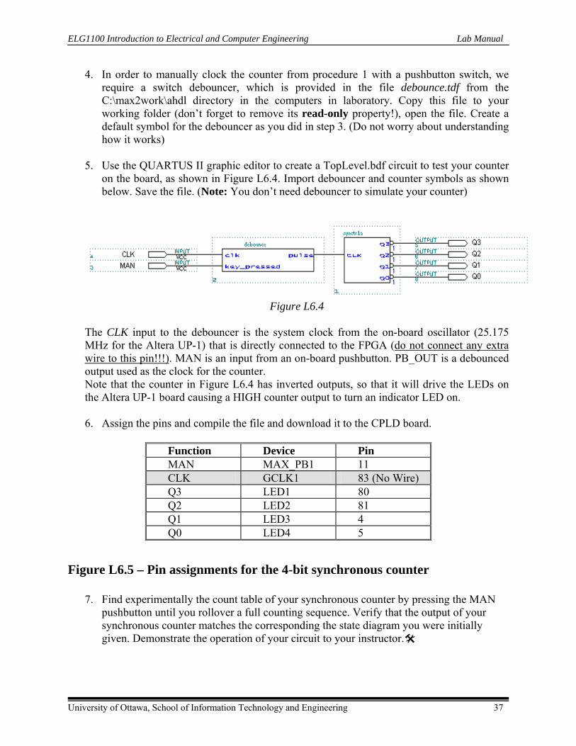
5. Use the QUARTUS II graphic editor to create a TopLevel.bdf circuit to test your counter
on the board, as shown in Figure L6.4. Import debouncer and counter symbols as shown below. Save the file. (Note: You don’t need debouncer to simulate your counter)
Figure L6.4 The CLK input to the debouncer is the system clock from the on-board oscillator (25.175 MHz for the Altera UP-1) that is directly connected to the FPGA (do not connect any extra wire to this pin!!!). MAN is an input from an on-board pushbutton. PB_OUT is a debounced output used as the clock for the counter. Note that the counter in Figure L6.4 has inverted outputs, so that it will drive the LEDs on the Altera UP-1 board causing a HIGH counter output to turn an indicator LED on. 6. Assign the pins and compile the file and download it to the CPLD board.
Function Device Pin MAN MAX_PB1 11 CLK GCLK1 83 (No Wire) Q3 LED1 80 Q2 LED2 81 Q1 LED3 4 Q0 LED4 5
Figure L6.5 – Pin assignments for the 4-bit synchronous counter 7. Find experimentally the count table of your synchronous counter by pressing the MAN
pushbutton until you rollover a full counting sequence. Verify that the output of your synchronous counter matches the corresponding the state diagram you were initially given. Demonstrate the operation of your circuit to your instructor.
University of Ottawa, School of Information Technology and Engineering 37

ELG1100 Introduction to Electrical and Computer Engineering Lab Manual
ITI1100 Laboratory Manual 38