
IS31SE5100 - ISSI · IS31SE5100 Integrated Silicon Solution, Inc. ... CAP5 CAP6 CAP7 CAP8 AD SCL...
13
IS31SE5100 Integrated Silicon Solution, Inc. – www.issi.com 1 Rev. C, 03/18/2013 8-CH CAPACITIVE TOUCH SENSOR WITH AUTO CALIBRATION March 2013 GENERAL DESCRIPTION The IS31SE5100 is an ultra low power, fully integrated 8-channel solution for capacitive touch-buttons applications. The chip allows electrodes to project sense fields through any dielectric such as glass or plastic. On-chip calibration logic continuously monitors the environment and automatically adjusts on-and-off threshold levels to prevent false sensor activation. The IS31SE5100 supports the 400kHz I²C serial bus data protocol and includes a field programmable slave address. An INTB is generated when a button event (touched or released) occurs, triggered and cleared condition could be configured by setting the interrupt register. IS31SE5100 is available in QFN-24 (4mm × 4mm) and SSOP-24 packages. It operates from 2.7V to 5.5V over the temperature range of -40°C to +85°C. FEATURES Complete eight sensors capacitive touch controller for buttons Auto offset compensation Sensitivity adjustable by external capacitor or internal register Extremely low power optimized for portable application Interrupt output 400kHz fast-mode I²C interface 8kV ESD HBM Operating temperature T A = −40°C ~ +85°C QFN-24 (4mm × 4mm) and SSOP-24 packages APPLICATIONS Mobile phones GPS PDAs TYPICAL APPLICATION CIRCUIT Figure 1 Typical Application Circuit Note 1: The IC should be placed far away from the mobile antenna in order to prevent the EMI. Note 2: The RS resistor should place as close as possible to reduce EMI.
Transcript of IS31SE5100 - ISSI · IS31SE5100 Integrated Silicon Solution, Inc. ... CAP5 CAP6 CAP7 CAP8 AD SCL...

IS31SE5100
Integrated Silicon Solution, Inc. – www.issi.com 1 Rev. C, 03/18/2013
8-CH CAPACITIVE TOUCH SENSOR WITH AUTO CALIBRATION
March 2013
GENERAL DESCRIPTION
The IS31SE5100 is an ultra low power, fully integrated 8-channel solution for capacitive touch-buttons applications. The chip allows electrodes to project sense fields through any dielectric such as glass or plastic. On-chip calibration logic continuously monitors the environment and automatically adjusts on-and-off threshold levels to prevent false sensor activation.
The IS31SE5100 supports the 400kHz I²C serial bus data protocol and includes a field programmable slave address. An INTB is generated when a button event (touched or released) occurs, triggered and cleared condition could be configured by setting the interrupt register.
IS31SE5100 is available in QFN-24 (4mm × 4mm) and SSOP-24 packages. It operates from 2.7V to 5.5V over the temperature range of -40°C to +85°C.
FEATURES
Complete eight sensors capacitive touch controller for buttons
Auto offset compensation Sensitivity adjustable by external capacitor or
internal register Extremely low power optimized for portable
application Interrupt output 400kHz fast-mode I²C interface 8kV ESD HBM Operating temperature TA = −40°C ~ +85°C QFN-24 (4mm × 4mm) and SSOP-24 packages
APPLICATIONS
Mobile phones GPS PDAs
TYPICAL APPLICATION CIRCUIT
Figure 1 Typical Application Circuit
Note 1: The IC should be placed far away from the mobile antenna in order to prevent the EMI.
Note 2: The RS resistor should place as close as possible to reduce EMI.

IS31SE5100
Integrated Silicon Solution, Inc. – www.issi.com 2 Rev. C, 03/18/2013
PIN CONFIGURATION
Package Pin Configuration (Top View)
QFN-24
1
2
3
4
24
14
15
16
17
23 22 21
7 8 9 10
5
11
18
20
6
12
13
19
CA
P5
CA
P6
CA
P7
CA
P8
AD
SC
L
SDA
INTB
SDB
OUT1
OUT2
OUT3
CAP1
CAP4
CAP2
CAP3
VCC
GND
GN
D
OU
T4
OU
T5
OU
T6
OU
T7
OU
T8
SSOP-24
1
2
3
4 21
22
23
24
OUT8
OUT4
GND OUT3
GND
OUT5
OUT7
OUT6
5
6
7
8 17
18
19
20
CAP2
OUT1
CAP3 INTB
SDB
OUT2
CAP1
VCC
9
10
11
12 13
14
15
16
CAP5
SCL
CAP6 CAP7
AD
SDA
CAP8
CAP4

IS31SE5100
Integrated Silicon Solution, Inc. – www.issi.com 3 Rev. C, 03/18/2013
PIN DESCRIPTION
No. Pin Description
QFN SSOP
1,19 4,22 GND Ground.
2 5 VCC Power supply.
3~10 6~9, 11~13,10
CAP1~CAP8 Input sense channel 1 ~ 8. Each channel should connect to GND if it is not used and disabled by the 01h register (Page 8).
11 14 AD I2C address setting.
12 15 SCL I2C serial clock.
13 16 SDA I2C serial data.
14 17 INTB Interrupt output, active low.
15 18 SDB Shutdown the chip when pulled low.
16~18 19~21 OUT1~OUT3 Channel 1 ~ 3 outputs. Pull low when input sense channel is pressed. Each channel should be floating if it is not used.
20~24 23,24, 1~3
OUT4~OUT8 Channel 4 ~ 8 outputs. Pull low when input sense channel is pressed. Each channel should be floating if it is not used.
- Thermal Pad Connect to GND.
Copyright © 2013 Integrated Silicon Solution, Inc. All rights reserved. ISSI reserves the right to make changes to this specification and its products at any time without notice. ISSI assumes no liability arising out of the application or use of any information, products or services described herein. Customers are advised to obtain the latest version of this device specification before relying on any published information and before placing orders for products. Integrated Silicon Solution, Inc. does not recommend the use of any of its products in life support applications where the failure or malfunction of the product can reasonably be expected to cause failure of the life support system or to significantly affect its safety or effectiveness. Products are not authorized for use in such applications unless Integrated Silicon Solution, Inc. receives written assurance to its satisfaction, that: a.) the risk of injury or damage has been minimized; b.) the user assume all such risks; and c.) potential liability of Integrated Silicon Solution, Inc is adequately protected under the circumstances

IS31SE5100
Integrated Silicon Solution, Inc. – www.issi.com 4 Rev. C, 03/18/2013
ORDERING INFORMATION Industrial Range: -40°C to +85°C
Order Part No. Package QTY
IS31SE5100-QFLS2-TR
IS31SE5100-SALS2
QFN-24, Lead-free
SSOP-24, Lead-free
2500/Reel
58/Tube

IS31SE5100
Integrated Silicon Solution, Inc. – www.issi.com 5 Rev. C, 03/18/2013
ABSOLUTE MAXIMUM RATINGS
Supply voltage, VCC -0.3V ~ +6.0V Voltage at any input pin -0.3V ~ VCC+0.3V Maximum junction temperature, TJMAX 150°C Storage temperature range, TSTG -65°C ~ +150°C Operating temperature range, TA −40°C ~ +85°C
Note:
Stresses beyond those listed under “Absolute Maximum Ratings” may cause permanent damage to the device. These are stress ratings only and functional operation of the device at these or any other condition beyond those indicated in the operational sections of the specifications is not implied. Exposure to absolute maximum rating conditions for extended periods may affect device reliability.
ELECTRICAL CHARACTERISTICS
TA = 25°C, VCC = 2.7V ~ 5.5V, unless otherwise noted. Typical value are TA = 25°C, VCC = 3.6V.
Symbol Parameter Condition Min. Typ. Max. Unit
VCC Supply voltage 2.7 5.5 V
ICC Quiescent power supply current VSDB = VCC = 3.6V 11 175 345 μA
ISD Shutdown current VSDB = 0V, VCC = 5.5V 0 0.5 2.3 μA
VHR Current Sink headroom voltage IOUT = 20mA, VCC = 3.6V 218 312 412 mV
∆CS Minimum detectable capacitance CS = 5pF (Note 1) 0.2 pF
Logic Electrical Characteristics
VIL Logic “0” input voltage VCC = 2.7V 0.4 V
VIH Logic “1” input voltage VCC = 5.5V 1.4 V
IIL Logic “0” input current VINPUT = 0V(Note 1) 5 nA
IIH Logic “1” input current VINPUT = VCC(Note 1) 5 nA
DIGITAL INPUT SWITCHING CHARACTERISTICS (Note 1)
Symbol Parameter Condition Min. Typ. Max. Unit
fSCL Serial-Clock frequency 400 kHz
tBUF Bus free time between a STOP and a START condition
1.3 μs
tHD, STA Hold time (repeated) START condition 0.6 μs
tSU, STA Repeated START condition setup time 0.6 μs
tSU, STO STOP condition setup time 0.6 μs
tHD, DAT Data hold time 0.9 μs
tSU, DAT Data setup time 100 ns
tLOW SCL clock low period 1.3 μs
tHIGH SCL clock high period 0.7 μs
tR Rise time of both SDA and SCL signals, receiving
(Note 2) 20+0.1Cb 300 ns
tF Fall time of both SDA and SCL signals, receiving
(Note 2) 20+0.1Cb 300 ns
Note 1: Guaranteed by design.
Note 2: Cb = total capacitance of one bus line in pF. ISINK ≤ 6mA. tR and tF measured between 0.3 × VCC and 0.7 × VCC.
IS31SE5100
Integrated Silicon Solution, Inc. – www.issi.com 6 Rev. C, 03/18/2013
DETAILED DESCRIPTION
I2C INTERFACE
The IS31SE5100 uses a serial bus, which conforms to the I2C protocol, to control the chip’s functions with two wires: SCL and SDA. The IS31SE5100 has a 7-bit slave address (A7:A1), followed by the R/W bit, A0. Set A0 to “0” for a write command and set A0 to “1” for a read command. The value of bits A1 and A2 are decided by the connection of the AD pin.
The complete slave address is:
Table 1 Slave Address
Bit A7:A3 A2:A1 A0
Value 10001 AD 1/0
AD connected to GND, AD = 00; AD connected to VCC, AD = 11; AD connected to SCL, AD = 01; AD connected to SDA, AD = 10;
The SCL line is uni-directional. The SDA line is bi-directional (open-collector) with a pull-up resistor (typically 4.7kΩ). The maximum clock frequency specified by the I2C standard is 400kHz. In this discussion, the master is the microcontroller and the slave is the IS31SE5100.
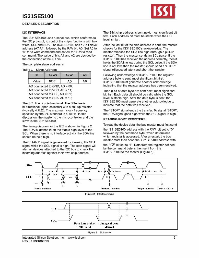
The timing diagram for the I2C is shown in Figure 2. The SDA is latched in on the stable high level of the SCL. When there is no interface activity, the SDA line should be held high.
The “START” signal is generated by lowering the SDA signal while the SCL signal is high. The start signal will alert all devices attached to the I2C bus to check the incoming address against their own chip address.
The 8-bit chip address is sent next, most significant bit first. Each address bit must be stable while the SCL level is high.
After the last bit of the chip address is sent, the master checks for the IS31SE5100’s acknowledge. The master releases the SDA line high (through a pull-up resistor). Then the master sends an SCL pulse. If the IS31SE5100 has received the address correctly, then it holds the SDA line low during the SCL pulse. If the SDA line is not low, then the master should send a “STOP” signal (discussed later) and abort the transfer.
Following acknowledge of IS31SE5100, the register address byte is sent, most significant bit first. IS31SE5100 must generate another acknowledge indicating that the register address has been received.
Then 8-bit of data byte are sent next, most significant bit first. Each data bit should be valid while the SCL level is stable high. After the data byte is sent, the IS31SE5100 must generate another acknowledge to indicate that the data was received.
The “STOP” signal ends the transfer. To signal “STOP”, the SDA signal goes high while the SCL signal is high.
READING PORT REGISTERS
To read the device data, the bus master must first send
the IS31SE5100 address with the R/W____
bit set to “0”, followed by the command byte, which determines which register is accessed. After a restart, the bus master must then send the IS31SE5100 address with
the R/W____
bit set to “1”. Data from the register defined by the command byte is then sent from the IS31SE5100 to the master (Figure 5).
Figure 2 Interface timing
Figure 3 Bit transfer

IS31SE5100
Integrated Silicon Solution, Inc. – www.issi.com 7 Rev. C, 03/18/2013
Figure 4 Writing to IS31SE5100
Figure 5 Reading from IS31SE5100

IS31SE5100
Integrated Silicon Solution, Inc. – www.issi.com 8 Rev. C, 03/18/2013
Table 2 Register Function
Address Name Function Table Default
00h Configuration Register Set software shutdown mode and sensitivity 3 0000 0000
01h Channel Control Register Set the 8 channels enable 4 1111 1111
02h State Register 1 Store state of action for 8 channels 5
0000 0000 03h State Register 2 Show state of 8 channels changes or not 6
04h Interrupt Register Set interrupt function 7
Table 3 00h Configuration Register
Bit D7 D6:D5 D4:D0
Name SSD SS -
Default 0 00 00000
The Configuration Register sets software shutdown mode and sensitivity. SSD Software Shutdown Enable 0 Normal operation 1 Software shutdown mode
SS Sensitivity Selection 00 Normal sensitivity 01 High sensitivity 10 Low sensitivity 11 Not a valid state Table 4 01h Channel Control Register
Bit D7:D0
Name CH8: CH1
Default 1111 1111
The Channel Control Register sets the 8 channels enable. CHx Channel Enable 0 Disable 1 Enable
Table 5 02h State Register 1 (Read only)
Bit D7:D0
Name AS8: AS1
Default 0000 0000
The State Register 1 stores state of action for 8 channels. ASx Action State Bit 0 Button released 1 Button pressed Table 6 03h State Register 2 (Read only)
Bit D7:D1
Name SC8: SC1
Default 0000 0000
The State Register 2 shows state of 8 channels changes or not. SCx State Change Bit 0 No state change 1 Button touched or released event occurs Table 7 04h Interrupt Register
Bit D7:D6 D5:D0
Name ACI -
Default 00 000000
The Interrupt Register sets interrupt function. ACI Automatically Clear Interrupt 00 No auto clear 01 Auto clear after 8ms 10 Auto clear after 32ms 11 Not a valid state
IS31SE5100
Integrated Silicon Solution, Inc. – www.issi.com 9 Rev. C, 03/18/2013
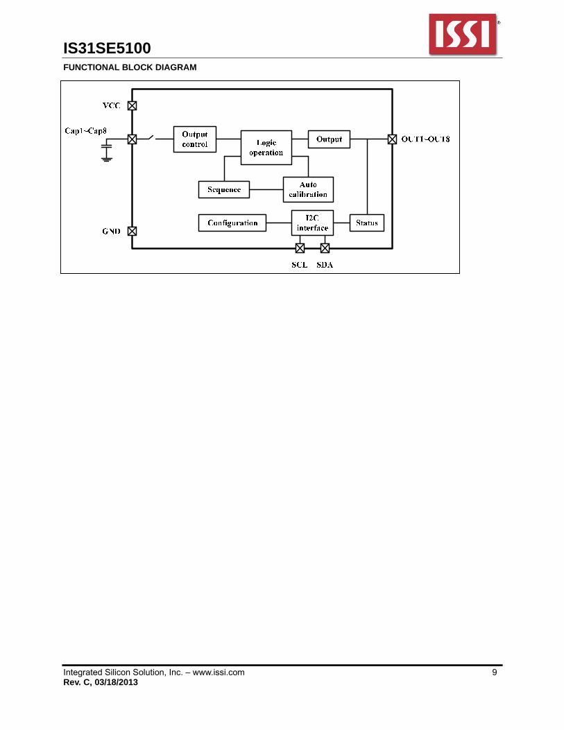
FUNCTIONAL BLOCK DIAGRAM

IS31SE5100
Integrated Silicon Solution, Inc. – www.issi.com 10 Rev. C, 03/18/2013
TYPICAL APPLICATION GENERAL DESCRIPTION
The IS31SE5100 is an ultra low power, fully integrated 8-channel solution for capacitive touch-buttons applications. The chip allows electrodes to project sense fields through any dielectric such as glass or plastic.
SENSITIVITY ADJUSTING
Sensitivity can be adjusted by the external capacitor or internal register.
The value of capacitor is higher the sensitivity is lower; value of capacitor is lower the sensitivity is higher.
The SS bit of Configuration Register (00h) is used to modulate sensitivity. By setting the SS bit to “00” sensitivity is normal. Sensitivity is high when SS bit is set to “01”. Sensitivity is low when SS bit is set to “10”. Setting SS bit to “11” is not a valid state.
OUTPUT CONTROL
There are 8 output ports for 8 sensitivity channels. The corresponding output will be pulled low to drive LED or other device if sensitivity channel is pressed.
For example, in Figure 1, when some sensitivity channels are pressed, the corresponding LEDs will be light up.
ACTION INFORMATION
The action information is stored in the State Register (02h, 03h). If the AS bit is set to “0”, the corresponding channel is released. If the AS bit is set to “1”, the corresponding channels is pressed. If the SC bit is set to “0”, the corresponding channel has no status changing. If the SC bit is set to “1”, the corresponding channel has status changing.
INTERRUPTION
The changing of action can be signed by the INTB pin. The INTB pin will be pulled low when sensitivity channel is pressed or released. And the MCU can get the information via reading the Status Register (02h, 03h). The INTB will be back to high until the MCU reading the Status Register 2 (03h).
The ACI bit of Interrupt Register (04h) is used to configure the automatically interrupt function. If the ACI bit is set to “00”, the automatically interrupt function disable. If the ACI bit is set to “01”, the function enable and he INTB pin will be high automatically when it stays low last 8ms. If the ACI bit is set to “10”, the INTB pin will be high automatically when it stays low last 32ms. Setting ACI bit to “11” is not a valid state.
SHUTDOWN MODE
Shutdown mode can be used as a means of reducing power consumption. During shutdown mode all registers retain their data.
SOFTWARE SHUTDOWN
By setting SSD bit of the Configuration Register (00h) to “1”, the IS31SE5100 will operate in software shutdown mode.
HARDWARE SHUTDOWN
The chip enters hardware shutdown mode when the SDB pin is pulled low, wherein they consume only 0.5μA (typ.) current.

IS31SE5100
Integrated Silicon Solution, Inc. – www.issi.com 11 Rev. C, 03/18/2013
CLASSIFICATION REFLOW PROFILES Profile Feature Pb-Free Assembly
Preheat & Soak
Temperature min (Tsmin) Temperature max (Tsmax) Time (Tsmin to Tsmax) (ts)
150°C 200°C 60-120 seconds
Average ramp-up rate (Tsmax to Tp) 3°C/second max.
Liquidous temperature (TL) Time at liquidous (tL)
217°C 60-150 seconds
Peak package body temperature (Tp)* Max 260°C
Time (tp)** within 5°C of the specified classification temperature (Tc)
Max 30 seconds
Average ramp-down rate (Tp to Tsmax) 6°C/second max.
Time 25°C to peak temperature 8 minutes max.
Figure 6 Classification profile

IS31SE5100
Integrated Silicon Solution, Inc. – www.issi.com 12 Rev. C, 03/18/2013
PACKAGE INFORMATION QFN-24

IS31SE5100
Integrated Silicon Solution, Inc. – www.issi.com 13 Rev. C, 03/18/2013
SSOP-24
Note: All dimensions in millimeters unless otherwise stated.


![F3JR MB R20 1211[31731]ncandelier.free.fr/asus/ASUS_F3JR_R20.pdfH_D#50 H_TMS H_TDO H_TCK H_TRST# H_PREQ# +VCCP +VCCP +VCCP +VCCP GND GND GND GND GND GND GND TPC26T 1 T1 R8 1 2 56Ohm](https://static.fdocuments.us/doc/165x107/5faf0ab01979a324157ec2b6/f3jr-mb-r20-121131731-hd50-htms-htdo-htck-htrst-hpreq-vccp-vccp-vccp.jpg)


