Introduction to FPGA Circuits -...
27
Introduction to FPGA Circuits Arnaud Tisserand CNRS, IRISA laboratory, CAIRN research team ´ Ecole ARCHI Col-de-Porte, Is` ere March 25–29th 2013 Summary Part I Introduction Implementations Targets Historical Aspects FPGA Overview Economic Issues Part II FPGA Elements Logic Blocks Routing I/O Blocks Clock Resources Hard RAM Blocks Hard DSP Blocks Part III Processors in FPGAs Motivations for Processors in FPGAs Hard Block Processors Soft-Core Processors Part IV References Journals and Conferences Articles and Chapters Books A. Tisserand, CNRS–IRISA–CAIRN. Introduction to FPGA Circuits 2/107 Part I Introduction Implementations Targets Historical Aspects FPGA Overview Economic Issues A. Tisserand, CNRS–IRISA–CAIRN. Introduction to FPGA Circuits 3/107 Software versus Hardware Implementation reg. file FU 1 FU 2 FU 3 LSU memory hierarchy D instructions managment + control I @ @ SW HW CTRL op. reg. op. reg. op. reg. op. reg. memory FLEXIBILITY EXCELLENT limited SPEED slow fast AREA large small ENERGY large small DEVEL. COST small HUGE A. Tisserand, CNRS–IRISA–CAIRN. Introduction to FPGA Circuits 4/107
-
Upload
hoangkhanh -
Category
Documents
-
view
259 -
download
0
Transcript of Introduction to FPGA Circuits -...

Introduction to FPGA Circuits
Arnaud Tisserand
CNRS, IRISA laboratory, CAIRN research team
Ecole ARCHICol-de-Porte, Isere
March 25–29th 2013
Summary
Part I
Introduction
Implementations TargetsHistorical AspectsFPGA OverviewEconomic Issues
Part II
FPGA Elements
Logic BlocksRoutingI/O BlocksClock ResourcesHard RAM BlocksHard DSP Blocks
Part III
Processors in FPGAs
Motivations for Processors in FPGAsHard Block ProcessorsSoft-Core Processors
Part IV
References
Journals and ConferencesArticles and ChaptersBooks
A. Tisserand, CNRS–IRISA–CAIRN. Introduction to FPGA Circuits 2/107
Part I
Introduction
Implementations Targets
Historical Aspects
FPGA Overview
Economic Issues
A. Tisserand, CNRS–IRISA–CAIRN. Introduction to FPGA Circuits 3/107
Software versus Hardware Implementation
reg.file
FU1 FU2 FU3LSU
mem
ory
hie
rarc
hy
D
instructions managment + controlI
@@
SW
HW
CT
RL
op
.
reg
.
op
.
reg
.
op
.
reg
.
op
.
reg
.
memory
FLEXIBILITY
EXCELLENT
limited
SPEED
slow
fast
AREA
large
small
ENERGY
large
small
DEVEL. COST
small
HUGE
A. Tisserand, CNRS–IRISA–CAIRN. Introduction to FPGA Circuits 4/107

Implementations Targets
choice?
software
hardware
GPP: general purpose processorIntel Core i3-5-7 & Xeon, AMD Athlon & Opteron
ARM Cortex Ax, Cell, Power. . .
ASP: application specific processorDSP digital signal processors: C60000, MSC81xx.. . .
network proc., security proc., power manager.. . .
µcontroller8051, AVR, ColdFire, MSP, PIC. . .
full-custom circuitscustomize all elements and layers
standard-cell circuitsfunctions = cells from library, only “draw” connexions
gate-arrays circuits1) predefined but unconnected transistors (active elem.)2) connections using top metals
FL
EX
IBIL
ITY
PE
RF
OR
MA
NC
ES
+ FPGA
A. Tisserand, CNRS–IRISA–CAIRN. Introduction to FPGA Circuits 5/107
Full-Custom vs. Standard Cell vs. Gate Arrays
gate arraystandard cellfull custom
perfs +++
costs +++
perfs ++
costs ++
perfs +
costs +
A. Tisserand, CNRS–IRISA–CAIRN. Introduction to FPGA Circuits 6/107
PLA: Programmable Logic Array
• User programmable device for combinational logic (197x)
• Sum-of-product canonical form
• Crossing planes of wires before configuration
• Configuration (programming): (un)set (un)wanted connections
• Inputs xi (xi ), outputs yj
p1 = x1x2
p2 = x2x3
p3 = x1x3
p4 = x1x2x3
y1 = x1x2 + x2x3 + x1x3
y2 = x2x3 + x1x2x3
x1
x2
x3
p1 p2 p3 p4 p5 p6
y1
y2
ANDplane
ORplane
NORs / NANDs are used in practice for CMOS circuits.
A. Tisserand, CNRS–IRISA–CAIRN. Introduction to FPGA Circuits 7/107
Terminology
acronym type prog.
ASIC application-specific integrated circuit N
MPGA masked programmable logic array Y
PROM programmable read-only memory Y
EPROM erasable PROM Y
EEPROM electrically EPROM Y
PAL programmable array logic Y
PLA programmable logic array Y
GAL generic array logic1 Y
PLD programmable logic device Y
EPLD erasable PLD Y
SPLD simple PLD Y
CPLD complex PLD Y
FPGA field-programmable gate array Y
1 GALs 6= GALS (globally asynchronous locally synchronous)
A. Tisserand, CNRS–IRISA–CAIRN. Introduction to FPGA Circuits 8/107

From Gate-Arrays to FPGAs
End of book:Bob Hartmann, Paul Newhagen and Michael MagranetGate Arrays: Implementing LSI Technology, 1982
”The probabilities are high that someone will produce anelectrically alterable logic array.”
June 3rd, 1983:Foundation of the Altera society byBob Hartmann1, Paul Newhagen1, Michael Magranet1,Jim Sansburry2 and Jim Hazle1
Source: “Altera: A History of Innovation” from Altera website
1previously at Fairchild Semiconductor, 2previsouly at HP.
A. Tisserand, CNRS–IRISA–CAIRN. Introduction to FPGA Circuits 9/107
First Commercial FPGA
1984:Xilinx society founded by Ross Freeman and Bernard Vonderschmitt
1985: XC2064
• CMOS 2.5µm (Seiko), 85 kT
• ≈ 1000 gates
• 64 CLBs, 122 FFs, LUT3
• 58 I/O (68-pin PLCC package)
• 18 MHz ext. crystal oscillator
• Config.: 12 038 bits
Source: IEEE SSC Mag. Vol. 3 No. 4 2011 p. 18
& Xilinx Data Sheet
A. Tisserand, CNRS–IRISA–CAIRN. Introduction to FPGA Circuits 10/107
History of PLD Startups
Source: EE TimesA. Tisserand, CNRS–IRISA–CAIRN. Introduction to FPGA Circuits 11/107
FPGAs Application Domains
• ASIC Prototyping
• Audio, video & image processing
• Automotive
• Aviation
• Consumer Electronics
• Industrial
• Test & measures
• Networks, wired and wireless communications
• Data centers, high-performance computing and storage
• Medical
• Security and defense
• Aerospace
• . . .
A. Tisserand, CNRS–IRISA–CAIRN. Introduction to FPGA Circuits 12/107

Xilinx FPGAs on MARS!
“According to NASA’s Jet Propulsion Laboratory in Pasadena, California,the Spirit Mars Exploration Rover (MER) launched June 10, 2003 and theOpportunity MER launched July 7, 2003 will employ some of the mostadvanced radiation tolerant Xilinx Virtex FPGAs once they reach Mars.The Xilinx devices will be used to control the pyrotechnic devices on thelander, and several motor control functions on the rover, includingcontrollers for the wheels, steering, and antenna gimbals.
Chosen because of their re-programmability and density, the Virtex FPGAsserve as the ’main brain’ of the motor control boards. ”
Source: Xilinx press release n. 03104, 2003, July 21st, San Jose, California.
See also: http://www.xilinx.com/publications/archives/xcell/Xcell50.pdf
A. Tisserand, CNRS–IRISA–CAIRN. Introduction to FPGA Circuits 13/107
FPGA Overview
active layer
specific I/O block
transceiver
config block
clock manag. & distrib.
logic blockrouting
I/O block
RAM block
DSP block
hard processor
virtual configuration layer
A. Tisserand, CNRS–IRISA–CAIRN. Introduction to FPGA Circuits 14/107
Configuration Cell Technology: Anti-Fuse (1/2)Principle:
wire
wire
AF
beforeprog.
afterprog.
substrate
via
M1
M2
AF
Example:
• 15-20 A nitride-oxide (NO) dieletricbetween 2 polysilicon layers
• 5.5 V circuit supply voltage
• 13.6 V programming voltage
• 0.8 × 0.8µm cell footprint
Source: IEEE Electron Device Letters, vol. 12,
n. 4, pp. 151–153, 1991 (doi: 10.1109/55.75747)
A. Tisserand, CNRS–IRISA–CAIRN. Introduction to FPGA Circuits 15/107
Configuration Cell Technology: Antifuse (2/2)
Cross section of antifuses in ACTEL (now Microsemi) FPGAs:
Unprogrammed Programmed
A. Tisserand, CNRS–IRISA–CAIRN. Introduction to FPGA Circuits 16/107

Configuration Cell Technology: FLASH (1/2)
source drain
oxide control grid/gate (CG)
floating grid/gate (FG)
VGS
ID
VT1 VT2
emp
ty
char
ged
floating grid state
• Electrons can be trapped in the FG• Threshold voltage (VT ) depends on the charge in the FG• READ: apply intermediate voltage on the CG, then sense channel• STORE: inject electrons in the FG• ERASE: remove electrons from the FG (tunneling)
Source: http://www.actel.com/products/solutions/security/securitydevicearch.aspx
A. Tisserand, CNRS–IRISA–CAIRN. Introduction to FPGA Circuits 17/107
Configuration Cell Technology: FLASH (2/2)FLASH cell evolution for data storage (not always applicable to FPGAs)
Source: Proc. IEEE, vol. 91, n. 4, pp. 503-522, 2003 (doi:10.1109/JPROC.2003.811703 )A. Tisserand, CNRS–IRISA–CAIRN. Introduction to FPGA Circuits 18/107
Configuration Cell Technology: SRAM
1-bit static RAM cell (std. CMOS techno.) for each programmable element
config. data
write config.
prog. element
Source: Microelectronics J., vol. 42,
n. 11, pp. 1187-1207, 2011
(doi:10.1016/j.mejo.2011.07.008)
A. Tisserand, CNRS–IRISA–CAIRN. Introduction to FPGA Circuits 19/107
Typical FPGA Configuration Cell Types
FPGA configuration cell
volatile cellnon-volatile cell
antifuse FLASH SRAM
reconfigurable: no yes yes
config. at power down: saved saved lost
fabrication process: special FLASH std. CMOS
radiation tolerance: very good good medium
A. Tisserand, CNRS–IRISA–CAIRN. Introduction to FPGA Circuits 20/107

Overview of IC Production Economics (1/2)
C =F
N+ V
• C cost per circuit
• F fixed costs F = FNRE + Fother
I FNRE non-recurring engineering costs: prototyping, masks, packagingtooling, personnel costs, training, support, CAD tools, computers, . . .
I Fother all other fixed costs: documentation, marketing, administration,after-sales, . . .
• N number of circuits to sell
• V variable cost per circuit V = Vprocess + Vpackaging + Vtest
I Vprocess cost for producing one die
I Vpackaging package and “transformations” costs
I Vtest cf. specific course (depends on complexity and duration)
A. Tisserand, CNRS–IRISA–CAIRN. Introduction to FPGA Circuits 21/107
Overview of IC Production Economics (2/2)
Vprocess =W
K · YW · YPK = π
(r 2
A− 2r√
2A
)• W wafer cost (depends on process technology and wafer radius r)
• K number of complete die per wafer
• YW die yield per wafer
• YP packaging yield
• A die area
A. Tisserand, CNRS–IRISA–CAIRN. Introduction to FPGA Circuits 22/107
Economic Motivations for FPGAs vs ASICs (1/4)
Time to market (TTM):
AS
ICF
PG
A
time
specifications
system design
system verification
fabrication
system integration
production
shipping
GAIN
A. Tisserand, CNRS–IRISA–CAIRN. Introduction to FPGA Circuits 23/107
Economic Motivations for FPGAs vs ASICs (2/4)
Early arrival on the market:
time
revenue
MARKET WINDOWstart end
FPGA
TTM ASICTTM
Longer product life due to reconfigurability:
time
revenue
MARKET WINDOW
ASICFPGA
A. Tisserand, CNRS–IRISA–CAIRN. Introduction to FPGA Circuits 24/107
Economic Motivations for FPGAs vs ASICs (3/4)
FPGA domain vs ASIC domain (arbitrary scales):
FPGA domain ASIC domainFPGA domain ASIC domain
volume
total cost
n n + m n + 2m
“new”
“old”
ASIC
“old” “new”FPGA
A. Tisserand, CNRS–IRISA–CAIRN. Introduction to FPGA Circuits 25/107
Economic Motivations for FPGAs vs ASIC (4/4)
ASIC advantages:
• ultra high performances and very low power
• low unit cost
• small form factor
FPGA advantages:
• simple design and verification cycles
• no NRE costs
• low (re)design risk
• fast time to market
• reconfiguration (flexible systems)
A. Tisserand, CNRS–IRISA–CAIRN. Introduction to FPGA Circuits 26/107
Economic Aspects: Altera Corp. Values for 2012 (1/2)Net sales: 1 783 035 $ ≈ 2 600 employees worldwide
Main markets:
44%
21%
17%18%
Telecom & WirelessIndustrial Automation, Military & Automotive
Networking, Computer & Storage
Other
Geographic sales distribution:
43%
25%
18%
14%
Asia PacificEurope, Middle East and Africa
AmericasJapan
Source: Altera website http://investor.altera.com/, News ReleaseA. Tisserand, CNRS–IRISA–CAIRN. Introduction to FPGA Circuits 27/107
Economic Aspects: Altera Corp. Values for 2012 (2/2)
Products categories:
84%
9%7%
FPGA
CPLD
Other
32%
30%
38%
New (Stratix IV/V, Arria II/V, Cyclone IV/V, . . . )
Mainstream (Stratix III, Cyclone III, . . . )
Mature and Other
Source: Altera website http://investor.altera.com/, News Release
A. Tisserand, CNRS–IRISA–CAIRN. Introduction to FPGA Circuits 28/107

Economic Aspects: Xilinx Corp. Values for 2012 (1/2)Net sales: 2 240 700 $ ≈ 3 400 employees worldwide
Main markets:
47%
36% 15%
2%
Communications & Data Center
Industrial & A & DBroadcast, Consumer & Auto
Other
Geographic sales distribution:
34%
32%
25%
10%
Asia Pacific
North AmericaEurope
Japan
Source: Xilinx website http://investor.xilinx.com/releases.cfm, Investor FactsheetA. Tisserand, CNRS–IRISA–CAIRN. Introduction to FPGA Circuits 29/107
Economic Aspects: Xilinx Corp. Values for 2012 (2/2)
41%
25%
30%
4%
Mainstream
New
BaseSupport
Source: Xilinx website http://investor.xilinx.com/releases.cfm, Investor Factsheet
A. Tisserand, CNRS–IRISA–CAIRN. Introduction to FPGA Circuits 30/107
FPGA Companies
Achronix Semiconductor www.achronix.com
Altera www.altera.com
Lattice Semiconductor www.latticesemi.com
Microsemi (previously Actel) www.microsemi.com
QuickLogic www.quicklogic.com
Tabula www.tabula.com
Xilinx www.xilinx.com
A. Tisserand, CNRS–IRISA–CAIRN. Introduction to FPGA Circuits 31/107
FPGA Companies Revenues over 1999–2012
0.0
0.5
1.0
1.5
2.0
2.5
1999 2000 2001 2002 2003 2004 2005 2006 2007 2008 2009 2010 2011 2012
year
$billion
Altera
Xilinx
Source: FPGA companies websites
A. Tisserand, CNRS–IRISA–CAIRN. Introduction to FPGA Circuits 32/107

Reconfigurable Architectures
• Fine grain reconfigurable architectures:
Def.: reconfiguration at the bit/signal/gate level
Pros.: huge flexibility
Cons.: high configuration cost (area, time)
Examples: FPGAs
• Coarse grain reconfigurable architectures
Def.: reconfiguration at the function/bloc level:
Pros.: small configuration cost
Cons.: limited flexibility
Examples: TensilicaExamples: DART (IRISA), Systolic Ring (LIRMM), . . .
A. Tisserand, CNRS–IRISA–CAIRN. Introduction to FPGA Circuits 33/107
Part II
FPGA Elements
Logic Blocks
Routing
I/O Blocks
Clock Resources
Hard RAM Blocks
Hard DSP Blocks
A. Tisserand, CNRS–IRISA–CAIRN. Introduction to FPGA Circuits 34/107
Logic BlockResources:
• input and output pins
• configurable logic function generator(s) (FG)f is an arbitrary function of the inputs
• flip-flop(s) some intermediate registers and pipelining
• configurable internal selection and routing between resources
LOGIC BLOCK
inp
uts
outp
ut
I0
I1
I2
I3
FGf (I0, I1, I2, I3)
clk
O
A. Tisserand, CNRS–IRISA–CAIRN. Introduction to FPGA Circuits 35/107
Look Up Tables (LUT)
• Programmable memory cells: configuration of the truth table for allpossible values
• Address bits: selection of the truth table line
• Typical LUT types: 1 or 2 outputs, 3 to 6 inputs
sLUT
s
a 0
a 3
a 2
a 1
a 0
a 3
a 2
a 1
A. Tisserand, CNRS–IRISA–CAIRN. Introduction to FPGA Circuits 36/107

One Possible Implementation of a LUT-3
con
figu
rab
lem
emor
yp
oin
ts(≈
1by
teR
AM
)
000
001
010
011
100
101
110
111
a0 a1 a2
out
a0
a1
a2
out
A. Tisserand, CNRS–IRISA–CAIRN. Introduction to FPGA Circuits 37/107
Examples of LUT-4 Configurations
a3 1 1 1 1 1 1 1 1 0 0 0 0 0 0 0 0a2 1 1 1 1 0 0 0 0 1 1 1 1 0 0 0 0a1 1 1 0 0 1 1 0 0 1 1 0 0 1 1 0 0a0 1 0 1 0 1 0 1 0 1 0 1 0 1 0 1 0
f 1 0 0 0 0 0 0 0 0 0 0 0 0 0 0 0
a3 1 1 1 1 1 1 1 1 0 0 0 0 0 0 0 0a2 1 1 1 1 0 0 0 0 1 1 1 1 0 0 0 0a1 1 1 0 0 1 1 0 0 1 1 0 0 1 1 0 0a0 1 0 1 0 1 0 1 0 1 0 1 0 1 0 1 0
f 1 1 1 1 1 1 1 1 1 1 1 1 1 1 1 0
a3 1 1 1 1 1 1 1 1 0 0 0 0 0 0 0 0a2 1 1 1 1 0 0 0 0 1 1 1 1 0 0 0 0a1 1 1 0 0 1 1 0 0 1 1 0 0 1 1 0 0a0 1 0 1 0 1 0 1 0 1 0 1 0 1 0 1 0
f 0 1 1 0 1 0 0 1 1 0 0 1 0 1 1 0
A. Tisserand, CNRS–IRISA–CAIRN. Introduction to FPGA Circuits 38/107
XC 2064 Configurable Logic Block (CLB)
Source: Xilinx data sheet XC 2064/2018 Logic Cell Array p. 2.64
A. Tisserand, CNRS–IRISA–CAIRN. Introduction to FPGA Circuits 39/107
Actel ACT1 and ACT3 Logic Blocks
D00
D01
D10
D11
S1 S0
QDOUT
CLK CLRA1 B1 B0A0
ACT3ACT1
Source: Actel data sheet
A. Tisserand, CNRS–IRISA–CAIRN. Introduction to FPGA Circuits 40/107

Old Quicklogic Logic Block
OC
OR
OS
A1
A2
A3
A5
A6
B1
B2
C1
C2
D1
D2
E1
E2
F1
F2
F3
F4
F5
A4
F5
AZ
OZ
OZ
NZ
FZ
N
A
B
C
D
E
F
M
OS
D Q
Q
R
Source: Quicklogic data sheet
A. Tisserand, CNRS–IRISA–CAIRN. Introduction to FPGA Circuits 41/107
Xilinx XC3000 Logic Block
DI
A
B
C
D
E
LUT
RD
RG
O
1
CE
CLK
X
Y
Source: Xilinx data sheet
A. Tisserand, CNRS–IRISA–CAIRN. Introduction to FPGA Circuits 42/107
Carry Propagation Problem
Building high-speed addersis very costly using flexiblelogic blocks and generalrouting resources
Most of applications usemany adders
Parallel prefix adders:
0
4
3
2
1
5
6
Brent−Kung
15 14 13 12 11 10 9 8 7 6 5 4 3 2 1 0
0
2
1
3
Han−Carlson
4
5
15 14 13 12 11 10 9 8 7 6 5 4 3 2 1 0
A. Tisserand, CNRS–IRISA–CAIRN. Introduction to FPGA Circuits 43/107
Carry Propagation SolutionAdd dedicated resources for high-speed addition
There is a tradeoff between performances, cost and flexibility
LOGIC BLOCK
inp
uts
outp
ut
I0
I1
I2
I3
FGsum
carry propagation
cin
cout
clk
O
A. Tisserand, CNRS–IRISA–CAIRN. Introduction to FPGA Circuits 44/107
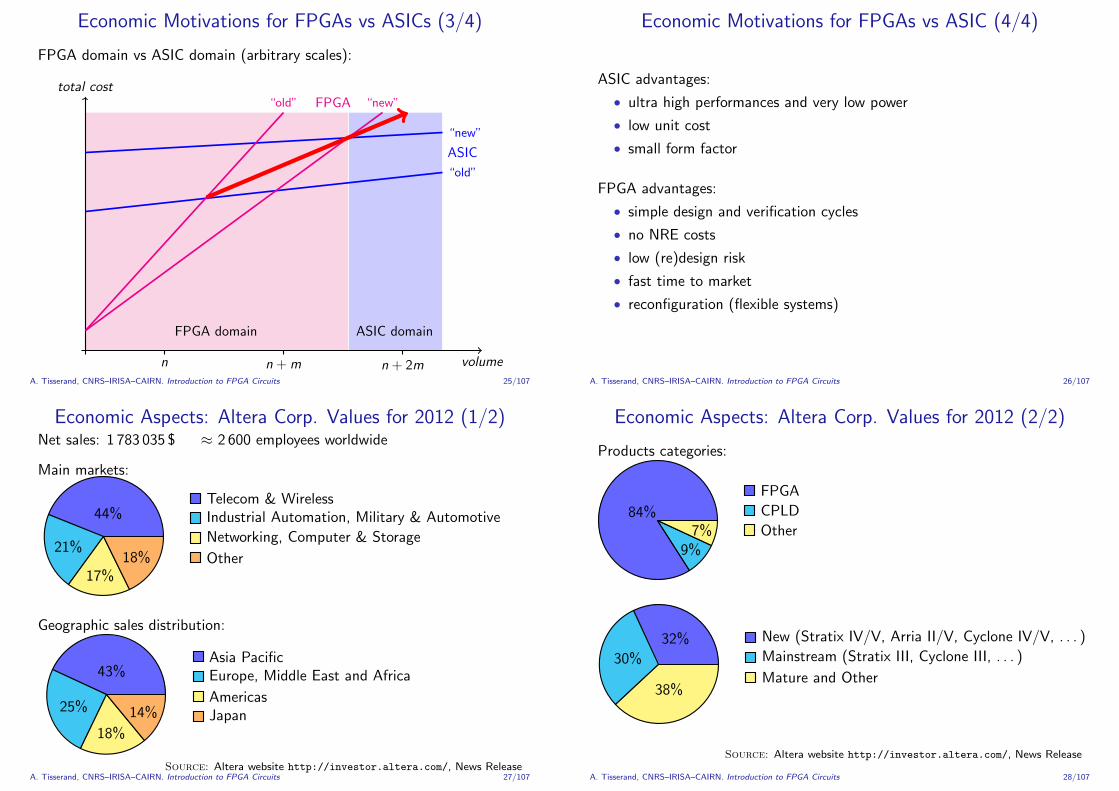
Carry Logic in a Xilinx XC 4000 E
Source: Xilinx data sheetA. Tisserand, CNRS–IRISA–CAIRN. Introduction to FPGA Circuits 45/107
Xilinx Spartan II E Configurable Logic Block
CA
RR
Y +
CT
RL
CA
RR
Y +
CT
RL
F1
COUT
CIN
XB
X
XQ
YQ
Y
YB
G4
G3
G2
G1
F5IN
BY
SR
F4
F3
F2
CE
CLK
BX
LUT
LUT DFF
DFF
A. Tisserand, CNRS–IRISA–CAIRN. Introduction to FPGA Circuits 46/107
Shift Registers in Logic Blocks
n
D Q D Q D Q D QD Qn
clk
LUT
clk
D Q31
n
Qn
A. Tisserand, CNRS–IRISA–CAIRN. Introduction to FPGA Circuits 47/107
Towards Larger LUTs
MUXF5
MUXF5
MUXF6
CLB
SLICE
LUT
LUT
LUT
LUT
A. Tisserand, CNRS–IRISA–CAIRN. Introduction to FPGA Circuits 48/107

Adaptive Logic Module in a Altera Stratix V
Source: Altera data sheet stx5 51002 p. 1.7A. Tisserand, CNRS–IRISA–CAIRN. Introduction to FPGA Circuits 49/107
Xilinx Virtex 7 Configurable Logic Block (1/3)
Source: Xilinx data sheet
UG474 p. 12
Resources per CLB:
Arithmetic &Slices LUT-6 Flip-Flops Carry Chains DRAM Shift Register
2 8 16 2 256 bits 128 bits
A. Tisserand, CNRS–IRISA–CAIRN. Introduction to FPGA Circuits 50/107
Xilinx Virtex 7 Configurable Logic Block (2/3)
SLICEM
Source: Xilinx data
sheet UG474 p. 14
A. Tisserand, CNRS–IRISA–CAIRN. Introduction to FPGA Circuits 51/107
Xilinx Virtex 7 Configurable Logic Block (3/3)
SLICEL
Source: Xilinx data
sheet UG474 p. 15
A. Tisserand, CNRS–IRISA–CAIRN. Introduction to FPGA Circuits 52/107

Evolution of Xilinx CLBs
XC 2000
LUTD Q
XC 3000
LUT
D Q
D Q
XC 4000
LUT
LUT
D Q
D Q
VIRTEX
slice
LUT
LUT propagation
D Q
D Q
slice
LUT
LUT propagation
D Q
D Q
VIRTEX 7
slice
LUT
LUT
LUT
LUT
propagation
+logique
D Q
D Q
D Q
D Q
slice
LUT
LUT
LUT
LUT
propagation
+logique
D Q
D Q
D Q
D Q
A. Tisserand, CNRS–IRISA–CAIRN. Introduction to FPGA Circuits 53/107
Typical Routing Overview
routing point
long line connexion
direct connexion
general purpose channel
logic block
switch matrix
A. Tisserand, CNRS–IRISA–CAIRN. Introduction to FPGA Circuits 54/107
Xilinx XC 3000 Switch Matrix
21 3 4 5
6 7 8 9 10
11 12 13 14 15
16 17 18 19 20
Source: Xilinx
data sheet
A. Tisserand, CNRS–IRISA–CAIRN. Introduction to FPGA Circuits 55/107
Routing Elements in Xilinx XC 4000 E
Source: Xilinx
data sheet
A. Tisserand, CNRS–IRISA–CAIRN. Introduction to FPGA Circuits 56/107

Routing Elements in a Xilinx Spartan II E
CLB CLB CLBCLB
Source: Xilinx data sheet
A. Tisserand, CNRS–IRISA–CAIRN. Introduction to FPGA Circuits 57/107
Routing Elements in Xilinx Virtex II
24 V24 H
120 H120 V
40 V40 H
16 8
Source: Xilinx data sheetA. Tisserand, CNRS–IRISA–CAIRN. Introduction to FPGA Circuits 58/107
Routing Elements in Xilinx Virtex 4 & Virtex 5
Virtex 4Virtex 5
CLB
1 lien
2 liens
3 liens
Source: Xilinx data sheet
A. Tisserand, CNRS–IRISA–CAIRN. Introduction to FPGA Circuits 59/107
Cross Section of a Virtex 5 FPGA 65 nm
12 metal layers (11 copper, 1 aluminium), 300 mm wafers, 1 V core supply
Source: http://www.eetimes.com/showArticle.jhtml?articleID=197003451
A. Tisserand, CNRS–IRISA–CAIRN. Introduction to FPGA Circuits 60/107

Input/Output Block in a Xilinx Virtex II
Q1
Q2
D1
CE
CLK1
SR
REV
CLK2
D2
OQ
3états
sortie
entrée
plot
Source: Xilinx data sheet
A. Tisserand, CNRS–IRISA–CAIRN. Introduction to FPGA Circuits 61/107
I/O Element in a Altera Stratix V
Source: Altera data sheet stx5 51006 p. 5.15A. Tisserand, CNRS–IRISA–CAIRN. Introduction to FPGA Circuits 62/107
I/O Have to Support Various Interface Standards
For “old” FPGAs:
TTL CMOS TTL/CMOS CMOS 3V
0.8 V0.4 V
2.7 V
0.5 V
3.5 V
1.0 V
4.5 V
3.9 V
0.8 V0.4 V
0.8 V0.4 V
2.4 V
3.3 V
0.0 V 0.0 V 0.0 V 0.0 V 0.0 V 0.0 V 0.0 V 0.0 V
2.0 V2.0 V2.0 V
5.0 V 5.0 V 5.0 V 5.0 V 5.0 V 5.0 V
3.3 V
5 V
4 V
3 V
2 V
1 V
0 V0
11
0
x
porteinV Vout
11
00
x
0
x
00
x
0
1
1
1 1
A. Tisserand, CNRS–IRISA–CAIRN. Introduction to FPGA Circuits 63/107
Some of the Supported Interface Standards in Virtex 7HSTL I DCI, DIFF HSTL I DCI, SSTL18 I DCI, DIFF SSTL18 I DCI, HSTL I DCI 18, DIFF HSTL I DCI 18,SSTL18 II DCI, DIFF SSTL18 II DCI, HSTL II DCI, DIFF HSTL II DCI, SSTL18 II T DCI, DIFF SSTL18 II T DCI,HSTL II DCI 18, DIFF HSTL II DCI 18, SSTL15 DCI, DIFF SSTL15 DCI, HSTL II T DCI, DIFF HSTL II T DCI,SSTL15 T DCI, DIFF SSTL15 T DCI, HSTL II T DCI 18, DIFF HSTL II T DCI 18, SSTL135 DCI, DIFF SSTL135 DCI,SSTL135 T DCI, DIFF SSTL135 T DCI, SSTL12 DCI, DIFF SSTL12 DCI, SSTL12 T DCI, DIFF SSTL12 T DCI
HSTL I DCI, DIFF HSTL I DCI, SSTL18 I DCI, DIFF SSTL18 I DCI, HSTL I DCI 18, DIFF HSTL I DCI 18,SSTL18 II DCI, DIFF SSTL18 II DCI, HSTL II DCI, DIFF HSTL II DCI, SSTL15 DCI, DIFF SSTL15 DCI,HSTL II DCI 18, DIFF HSTL II DCI 18, SSTL135 DCI, DIFF SSTL135 DCI, SSTL12 DCI, DIFF SSTL12 DCI
HSTL II T DCI, SSTL18 II T DCI, DIFF SSTL18 II T DCI, HSTL II T DCI 18, SSTL15 T DCI, DIFF SSTL15 T DCI,DIFF HSTL II T DCI, SSTL135 T DCI, DIFF SSTL135 T DCI , DIFF HSTL II T DCI 18, SSTL12 T DCI,DIFF SSTL12 T DCI
LVDCI 18, HSTL I DCI, DIFF HSTL I DCI, SSTL18 I DCI, DIFF SSTL18 I DCI, LVDCI 15, HSTL I DCI 18,DIFF HSTL I DCI 18, SSTL18 II DCI, DIFF SSTL18 II DCI, LVDCI DV2 18, HSTL II DCI, DIFF HSTL II DCI,SSTL18 II T DCI, DIFF SSTL18 II T DCI, LVDCI DV2 15, HSTL II DCI 18, DIFF HSTL II DCI 18, SSTL15 DCI,DIFF SSTL15 DCI, HSLVDCI 18, HSTL II T DCI, DIFF HSTL II T DCI, SSTL15 T DCI, DIFF SSTL15 T DCI,HSLVDCI 15, HSTL II T DCI 18, DIFF HSTL II T DCI 18, SSTL135 DCI, DIFF SSTL135 DCI, SSTL135 T DCI,DIFF SSTL135 T DCI, SSTL12 DCI, DIFF SSTL12 DCI, SSTL12 T DCI, DIFF SSTL12 T DCI, HSUL 12 DCI,DIFF HSUL 12 DCI
LVDCI 18, LVDCI DV2 18, HSLVDCI 18, HSUL 12 DCI, LVDCI 15, LVDCI DV2 15, HSLVDCI 15, DIFF HSUL 12 DCI
HSTL I, DIFF HSTL I, SSTL15 R, DIFF SSTL15 R, HSTL II, DIFF HSTL II, SSTL15, DIFF SSTL15, HSTL I 18,DIFF HSTL I 18, SSTL135 R, DIFF SSTL135 R, HSTL II 18, DIFF HSTL II 18, SSTL135, DIFF SSTL135, SSTL18 I,DIFF SSTL18 I, SSTL18 II, DIFF SSTL18 II,
Source: Xilinx data sheet ug471 7Series SelectIO.pdf
A. Tisserand, CNRS–IRISA–CAIRN. Introduction to FPGA Circuits 64/107

Packages for Xilinx Virtex II
package CS144 FG256 FG456 FG676 BG575 BG728 FF896 FF1152 FF1517 BF957
pitch (mm) 0.80 1.00 1.00 1.00 1.27 1.27 1.00 1.00 1.00 1.27
size (mm) 12x12 17x17 23x23 27x27 31x31 35x35 31x31 35x35 40x40 40x40
nb. I/O 92 172 324 484 408 516 624 824 1,108 684
FPGA→ XC2V
package ↓ 40 80 250 500 1000 1500 2000 3000 4000 6000 8000
CS144 88 92 92 - - - - - - - -
FG256 88 120 172 172 172 - - - - - -
FG456 - - 200 264 324 - - - - - -
FG676 - - - - - 392 456 484 - - -
FF896 - - - - 432 528 624 - - - -
FF1152 - - - - - - - 720 824 824 824
FF1517 - - - - - - - - 912 1 104 1 108
BG575 - - - - 328 392 408 - - - -
BG728 - - - - - - - 516 - - -
BF957 - - - - - - 624 684 684 684 -
Source: Xilinx data sheet
A. Tisserand, CNRS–IRISA–CAIRN. Introduction to FPGA Circuits 65/107
Some Packages used in FPGAs
CS144 Chip-ScaleBGA
1 2 3 4 5 6 7 8 9 10 11 12 13
M
L
K
J
I
H
G
F
E
D
C
B
A
12 mm
0.8 mm
1.2 mm
FF1517 Flip-Chip Fine-Pitch BGA40 mm
AJ
AH
AG
AF
AE
AD
AA
AB
AC
AK
AL
AM
J
H
G
F
E
D
A
B
C
K
L
M
1 mm
1 2 3 4 5 6 7 8 9 10 11 12 13
3.2 mm
AN
AP
AR
AT
AU
AV
AW
N
P
R
T
U
V
W
Y
14 15 16 17 18 19 20 21 22 23 24 25 26 27 28 29 30 31 32 33 34 35 36 37 38 39
A. Tisserand, CNRS–IRISA–CAIRN. Introduction to FPGA Circuits 66/107
Transceivers in Xilinx Virtex 6 & Virtex 7
Data rates:
40 nm 28 nm
type Spartan 6 Virtex 6 Artix 7 Kintex 7 Virtex 7
T XT HT
GTP 3.125 6.6
GTX 6.6 12.5 12.5 12.5
GTH 11.18 13.1 13.1
GTZ 28.05
A. Tisserand, CNRS–IRISA–CAIRN. Introduction to FPGA Circuits 67/107
Clock Generation in a Virtex II
DCM
BUF
CLK
CLKFB
CTRL
CLK0CLK90
CLK180CLK270CLKx2
CLK180x2CLKDIV
STATUS
DCM
signal
clock pad
internal
distrib. to region
DCM: digital clock manager
Possible clock division in a Virtex II: 1.5, 2, 2.5, 3, 3.5, 4, 4.5, 5, 5.5, 6,6.5, 7, 7.5, 8, 9, 10, 11, 12, 13, 14, 15, 16.
Source: Xilinx data sheet
A. Tisserand, CNRS–IRISA–CAIRN. Introduction to FPGA Circuits 68/107
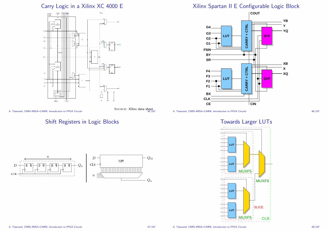
Clock Distribution in a Virtex II
NENW
SESW8
88
8
8 max
Source: Xilinx data sheet
A. Tisserand, CNRS–IRISA–CAIRN. Introduction to FPGA Circuits 69/107
Clocking Resources in a Virtex 6 (1/2)
MMCM: Mixed-Mode Clock Manager
Fout = Fin ×DI
DO6 to 18 clock regions depending on the FPGA size
Source: Xilinx data sheet: Virtex 6 FPGA Clocking Resources (UG362) p. 40
A. Tisserand, CNRS–IRISA–CAIRN. Introduction to FPGA Circuits 70/107
Clocking Resources in a Virtex 6 (2/2)
MMCM Application Example:
Source: Xilinx data sheet: Virtex 6 FPGA Clocking Resources (UG362) p. 61
A. Tisserand, CNRS–IRISA–CAIRN. Introduction to FPGA Circuits 71/107
Dedicated Hard Blocks of RAM in a Virtex II
• Single ou dual port 18 Kb BRAM (Block RAM)
• 4 (XC2V40) to 168 (XC2V8000) BRAMs
• Possible configurations for each BRAM:16K x 1, 8K x 2, 4K x 4, 1K x 18, 2K x 9, 512 x 36
Source: Xilinx Virtex II data sheet (DS083) pp. 44–46
A. Tisserand, CNRS–IRISA–CAIRN. Introduction to FPGA Circuits 72/107

BRAMs in a Virtex 7
• 36 Kb BRAMs
• 135 (XC7A100T) to1 880 (XC7VX1140T) BRAMs!!!
• RAM or FIFO configurations
• Cascade of 2 blocks
• ECC configurable support
Source: Xilinx Virtex 7 memory resource data
sheet (UG473)
A. Tisserand, CNRS–IRISA–CAIRN. Introduction to FPGA Circuits 73/107
Distributed RAM in a Virtex 7
SLICEMs distributed RAM configurationin a Virtex 7 CLB
#word× ports #
wordsize conf. R W LUT
32×1 S @1 @1 1
32×1 D @1@2 @1 2
32×2 Q @1@2@3@4 @1 4
32×6 SDP @1 @2 4
64×1 S @1 @1 1
64×1 D @1@2 @1 2
64×1 Q @1@2@3@4 @1 4
64×3 SDP @1 @2 4
128×1 S @1 @1 2
128×1 D @1@2 @1 4
256×1 Q @1@2@3@4 @1 4
Source: Xilinx Virtex 7 Configurable Logic Block User Guide (UG474)
A. Tisserand, CNRS–IRISA–CAIRN. Introduction to FPGA Circuits 74/107
Yet Another Dedicated Hard Block Type
Acc ←− Acc ± X ×Y
Multiply-and-accumulate is widely used in many applications:
• FIR and IIR filters
• FFT
• Matrix / vector computations
• Polynomial approximations
• Discrete Cosine Transform (DCT)
• . . .
=⇒ dedicated blocks
A. Tisserand, CNRS–IRISA–CAIRN. Introduction to FPGA Circuits 75/107
DSP Block Configuration in a Altera Stratix VVariable precision DSP bloc :• 2 multipliers 18× 18 bits per bloc• pre-adder/subtractor before the multipliers• adder/subtractor after the multipliers• e.g. (a× b)± (c × d)• 64-bit programmable accumulator (split 2 × 32)
in 1 bloc in 2 blocs
#op. op. #op. op.
3 x〈9〉 × y〈9〉 3 x〈18〉 × y〈18〉
2 x〈16〉 × y〈16〉 2 x〈27〉 × y〈27〉
x〈18〉 × y〈18〉 x〈36〉 × y〈36〉
1 x〈27〉 × y〈27〉 1 x〈18〉 ×C y〈18〉
x〈36〉 × y〈18〉
x〈n〉 denotes a n-bit operand x
Source: Altera data sheetA. Tisserand, CNRS–IRISA–CAIRN. Introduction to FPGA Circuits 76/107
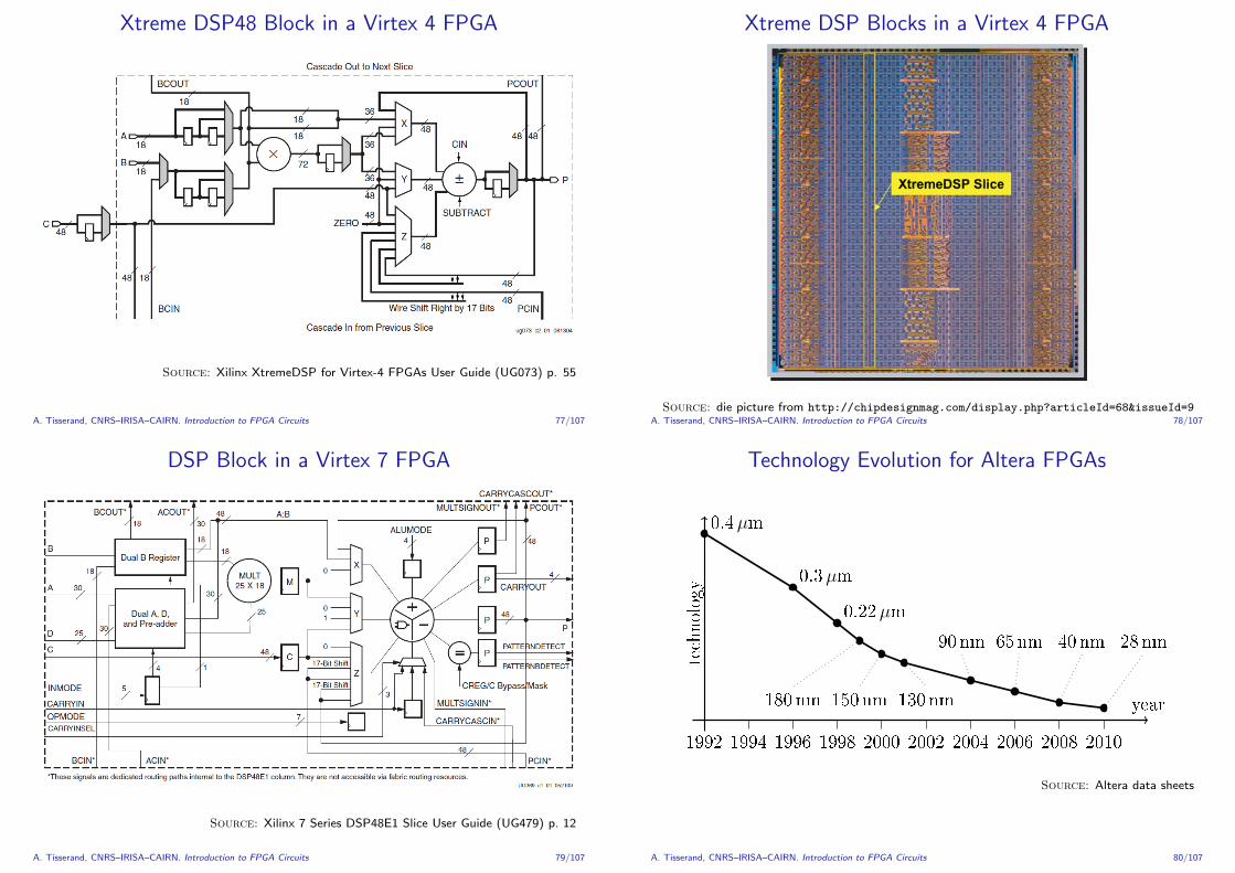
Xtreme DSP48 Block in a Virtex 4 FPGA
Source: Xilinx XtremeDSP for Virtex-4 FPGAs User Guide (UG073) p. 55
A. Tisserand, CNRS–IRISA–CAIRN. Introduction to FPGA Circuits 77/107
Xtreme DSP Blocks in a Virtex 4 FPGA
Source: die picture from http://chipdesignmag.com/display.php?articleId=68&issueId=9A. Tisserand, CNRS–IRISA–CAIRN. Introduction to FPGA Circuits 78/107
DSP Block in a Virtex 7 FPGA
Source: Xilinx 7 Series DSP48E1 Slice User Guide (UG479) p. 12
A. Tisserand, CNRS–IRISA–CAIRN. Introduction to FPGA Circuits 79/107
Technology Evolution for Altera FPGAs
yeartech
nology
1992 1994 1996 1998 2000 2002 2004 2006 2008 2010
0.4µm
0.3µm
0.22µm
180 nm 150 nm 130 nm
90 nm 65 nm 40 nm 28 nm
Source: Altera data sheets
A. Tisserand, CNRS–IRISA–CAIRN. Introduction to FPGA Circuits 80/107

Architecture Evolution for Altera FPGAs
Flex 8K
IO
IO
IO
IO IO IO
. . .
. . .
.
.
....
.
.
.
LAB
LE
Stratix V
IO
blocs
logiques
blocs
DSP
blocs
mémoire
blocs
logiques
blocs
DSP
blocs
mémoire
blocs
logiques
IO
Source: Altera data sheets
A. Tisserand, CNRS–IRISA–CAIRN. Introduction to FPGA Circuits 81/107
Altera FPGAs Evolution
Stratix
I II III IV V
year 2002 2004 2006 2008 2010
techno. [nm] 130 90 65 40 28
Vdd [V] 1.5 1.2 1.1 0.9 0.85
max. freq. [MHz] 350 450 550 600 700
# logic blocks 80 k 180 k 338 k 813 k 950 k
# DSP blocks [18×18] 88 384 768 1 288 4 096
RAM blocks [Mb] 7 9 18 23 33
transceivers 20 20 – 48 66
d.m.t. [Gb·s−1] 3.18 6.37 – 11.3 28
clocks glob./reg. 16/22 16/32 16/88 16/88 16/92
Source: Altera data sheets
A. Tisserand, CNRS–IRISA–CAIRN. Introduction to FPGA Circuits 82/107
Xilinx Spartan II Overview
IOB
CL
B
CL
B
CL
B
CL
B
CL
B
CL
B
CL
B
CL
B
CL
B
CL
B
CL
B
CL
B
CL
B
CL
B
CL
B
CL
B
CL
B
CL
B
CL
B
CL
B
CL
B
CL
B
CL
B
CL
B
CL
B
CL
B
CL
B
CL
B
CL
B
CL
B
CL
B
CL
B
CL
B
CL
B
CL
B
CL
B
CL
B
CL
B
CL
B
CL
B
CL
B
CL
B
CL
B
CL
B
CL
B
CL
B
CL
B
CL
B
CL
B
CL
B
CL
B
CL
B
CL
B
CL
B
CL
B
CL
B
CL
B
CL
B
CL
B
CL
B
CL
B
CL
B
CL
B
CL
B
BL
OC
K R
AM
BL
OC
K R
AM
BL
OC
K R
AM
BL
OC
K R
AM
DLL DLL
DLL DLL
A. Tisserand, CNRS–IRISA–CAIRN. Introduction to FPGA Circuits 83/107
Xilinx Spartan II FPGAs
# # equiv. matrix # # diff. DRAM BRAM
type gates gates L × C CLB I/O I/O bits bits
XC2S50E 1 728 23 000 – 50 000 16 × 24 384 182 83 24 576 32K
XC2S100E 2 700 37 000 – 100 000 20 × 30 600 202 86 38 400 40K
XC2S150E 3 888 52 000 – 150 000 24 × 36 864 265 114 55 296 48K
XC2S200E 5 292 71 000 – 200 000 28 × 42 1 176 289 120 75 264 56K
XC2S300E 6 912 93 000 – 300 000 32 × 48 1 536 329 120 98 304 64K
XC2S400E 10 800 145 000 – 400 000 40 × 60 2 400 410 172 153 600 160K
C2S600E 15 552 210 000 – 600 000 48 × 72 3 456 514 205 221 184 288K
Packages famille Spartan II E : TQ144, PQ208, FT256, FG456, FG676
Configuration bitstream size (in bits):
XC2S50E XC2S100E XC2S150E XC2S200E XC2S300E XC2S400E XC2S600E
630 048 863 840 1 134 496 1 442 016 1 875 648 2 693 440 3 961 632
A. Tisserand, CNRS–IRISA–CAIRN. Introduction to FPGA Circuits 84/107
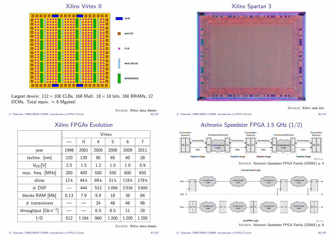
Xilinx Virtex II
BRAM(18Kb)
Mult (18x18)
CLB
plot E/S
DCM
Largest device: 112× 108 CLBs, 168 Mult. 18× 18 bits, 168 BRAMs, 12DCMs. Total equiv. ≈ 8 Mgates!
Source: Xilinx data sheetsA. Tisserand, CNRS–IRISA–CAIRN. Introduction to FPGA Circuits 85/107
Xilinx Spartan 3
Source: Xilinx web site
A. Tisserand, CNRS–IRISA–CAIRN. Introduction to FPGA Circuits 86/107
Xilinx FPGAs Evolution
Virtex
— II 4 5 6 7
year 1998 2001 2005 2006 2009 2011
techno. [nm] 220 130 90 65 40 28
VDD[V] 2.5 1.5 1.2 1.0 1.0 0.9
max. freq. [MHz] 200 400 500 550 600 650
slices 12 k 44 k 89 k 51 k 118 k 178 k
# DSP — 444 512 1 056 2 016 3 600
blocks RAM [Mb] 0.13 7.9 9.9 18 38 84
# transceivers — — 24 48 48 96
throughput [Gb·s−1] — — 6.5 6.5 11 28
I/O 512 1 164 960 1 200 1 200 1 200
Source: Xilinx data sheets
A. Tisserand, CNRS–IRISA–CAIRN. Introduction to FPGA Circuits 87/107
Achronix Speedster FPGA 1.5 GHz (1/2)
Source: Achronix Speedster FPGA Family (DS001) p. 4
Source: Achronix Speedster FPGA Family (DS001) p. 6
A. Tisserand, CNRS–IRISA–CAIRN. Introduction to FPGA Circuits 88/107

Achronix Speedster FPGA 1.5 GHz (2/2)
Source: Achronix Speedster FPGA Family (DS001) p. 6
A. Tisserand, CNRS–IRISA–CAIRN. Introduction to FPGA Circuits 89/107
Part III
Processors in FPGAs
Motivations for Processors in FPGAs
Hard Block Processors
Soft-Core Processors
A. Tisserand, CNRS–IRISA–CAIRN. Introduction to FPGA Circuits 90/107
Processors in FPGAs
Processors are widely used in electronic systems and FPGAs:
• the main processor at system level (32-bit, MMU, cache, “OSfriendly”, . . . )
• small processors (8/16-bit) used for local control (forcoprocessors/accelerators), “smart FSMs”
• FPGAs are larger and larger but implementing embedded processors isstill costly (area and design time)
• Embedded and low-power systems =⇒ single chip solution
Two solutions for embedded processors in FPGAs:
• dedicated hard blocks processor core(s)
• soft-core processors (synthezised on the FPGA resources)
A. Tisserand, CNRS–IRISA–CAIRN. Introduction to FPGA Circuits 91/107
PowerPC 405 in a Xilinx Virtex II (1/2)
• 0.13µm implementation of the IBMPowerPC 405D4 core
• 300 MHz+
• 32-bit address modes
• 64-bit operations
Source: xilinx data sheet (DS083) p. 29
A. Tisserand, CNRS–IRISA–CAIRN. Introduction to FPGA Circuits 92/107

PowerPC 405 in a Xilinx Virtex II (2/2)
Source: xilinx data sheet (DS083) p. 63
A. Tisserand, CNRS–IRISA–CAIRN. Introduction to FPGA Circuits 93/107
Xilinx Zynq 7000
Source: xilinx data sheet (DS190)
• hard block: dual-coreARM Cortex A9
• 28 nm implementation
• 667, 733, 800 MHz and1 GHz
• 1GB address space
• 64-bit operations
• Cache L1 I 32 KB4-way set-associative
• Cache L1 D 32 KB4-way set-associative
• Cache L2 I+D 512 KB8-way set-associative
• On-chip boot ROM
• 256 KB on-chip RAMA. Tisserand, CNRS–IRISA–CAIRN. Introduction to FPGA Circuits 94/107
Hard Processors Evolution in Xilinx FPGAs
Virtex Zynq
II Pro 4 5 7000
processor PowerPC PowerPC PowerPC ARM
405 405 440 Cortex A9
#core 1 or 2 1 or 2 1 or 2 1 double
max. freq. [MHz] 300 450 550 800
#pipe. stages 5 5 7 8
L1 [Ko] 16I+16D 16I+16D 32I+32D 32I+32D
L2 [Ko] — — — 512
o.o.o. no no yes yes
FPU no no no 32/64 b
Source: Xilinx data sheets
A. Tisserand, CNRS–IRISA–CAIRN. Introduction to FPGA Circuits 95/107
Soft-Core ProcessorsDefinition: embedded processor implemented using typical FPGA resources(logic blocks, RAM blocks, DSP blocks,. . . )
Examples:
pipe.
processor archi. #bit stages CPI MMU FPU license
NIOS II f NIOS II 32 6 1 yes opt. prop. Altera
NIOS II s NIOS II 32 5 1 no no prop. Altera
NIOS II e NIOS II 32 no 6 no no prop. Altera
MicroBlaze MicroBlaze 32 3 / 5 1 opt. opt. prop. Xilinx
PicoBlaze PicoBlaze 8 no 2 no no prop. Xilinx
Cortex M1 ARM V6 32 3 1 no yes prop. ARM
LEON 2 SPARC V8 32 5 1 yes yes LPGL
LEON 3 SPARC V8 32 7 1 yes yes GPL
OpenRISC OpenRISC
1200 1000 32 5 1 yes yes LGPL
. . .A. Tisserand, CNRS–IRISA–CAIRN. Introduction to FPGA Circuits 96/107

Xilinx MicroBlaze (1/2)
Source: Xilinx MicroBlaze Processor Reference Guide p. 9
A. Tisserand, CNRS–IRISA–CAIRN. Introduction to FPGA Circuits 97/107
Xilinx MicroBlaze (2/2)Supported FPGAs: Spartan 3/6, Virtex-4/5/6/7, Artix-7, Kintex-7,Zynq-7000
Various supported and optional features:
• Execution Hardware Acceleration• Instruction Set Extensions• Cache size configurable: 2kB to 64kB (BRAM)• Microcache size configurable: 64B to 1024B (DRAM)• Direct mapped write-through or write-back operation• Branch optimizations and prediction logic• Error Correction Codes (ECC)• Parity protection on internal BRAMs and caches• 32-bit Floating Point Unit (FPU) IEEE 754• Memory Management Unit (MMU)• MPU mode for region protection for secure RTOS applications• JTAG control via a debug support core
Source: Xilinx LogiCORE IP MicroBlaze (DS865)
A. Tisserand, CNRS–IRISA–CAIRN. Introduction to FPGA Circuits 98/107
Part IV
References
Journals and Conferences
Articles and Chapters
Books
A. Tisserand, CNRS–IRISA–CAIRN. Introduction to FPGA Circuits 99/107
Journals
• ACM Transactions on Reconfigurable Technology and Systems(TRETS)
• IEEE Transactions on Circuits and Systems (TCAS)
• IEEE Transactions on Computers (TC)
• IEEE Transactions on VLSI Systems (TVLSI)
• . . .
A. Tisserand, CNRS–IRISA–CAIRN. Introduction to FPGA Circuits 100/107

Conferences
Domain specific conferences:
• FPGA: ACM/SIGDA International Symposium on Field-ProgrammableGate Arrays
• FCCM: IEEE International Symposium on Field-Programmable CustomComputing Machines
• FPL: International Conference on Field Programmable Logic andApplications
• FPT: International Conference on Field-Programmable Technology
Sessions in general conferences:
• DAC: Design Automation Conference
• DATE: Design, Automation, and Test in Europe conference
• CHES: Workshop on Cryptographic Hardware and Embedded Systems
A. Tisserand, CNRS–IRISA–CAIRN. Introduction to FPGA Circuits 101/107
Articles and Chapters I
S. Brown.
FPGA architectural research: a survey.
IEEE Design & Test of Computers, 13(4):9–15, December 1996.
I. Kuon, R. Tessier, and J. Rose.
FPGA architecture: Survey and challenges.
Foundations and Trends in Electronic Design Automation, 2(2):135–253,2008.
O. Sentieys and A. Tisserand.
Architectures reconfigurables FPGA.
In Technologies logicielles Architectures des systemes, number H 1 196, pages1–22. Techniques de l’Ingenieur, August 2012.
A. Tisserand, CNRS–IRISA–CAIRN. Introduction to FPGA Circuits 102/107
Books on FPGAs (1/2)
FPGA Design
Best Practices for Team-Based Design
Philip Simpson
2010
Springer
ISBN: 978–1–4419–6339–0
FPGA Architecture
Survey and Challenges
Russell Tessier, Jonathan Rose and Ian Kuon
2008
Now Publishers Inc
ISBN: 978–1601981264
A. Tisserand, CNRS–IRISA–CAIRN. Introduction to FPGA Circuits 103/107
Books on FPGAs (2/2)
FPGA Design Automation
A Survey
Deming Chen, Jason Cong and Peichen Pan
2006
Now Publishers Inc
ISBN: 978-1933019383
A. Tisserand, CNRS–IRISA–CAIRN. Introduction to FPGA Circuits 104/107

Good Books: Circuit Technology & Design
CMOS VLSI Design
A Circuits and Systems Perspective
Neil Weste and David Harris
3rd edition, 2004
Addison Wesley
ISBN: 0–321–14901–7
Micro et nano-electronique
Bases, Composants, Circuits
Herve Fanet
2006
Dunod
ISBN: 2–10–049141–5
A. Tisserand, CNRS–IRISA–CAIRN. Introduction to FPGA Circuits 105/107
Other Topics on FPGAs
• Configuration
• Partial dynamic reconfiguration
• Low-power aspects
• Security aspects
• Programming
• CAD tools
• FPGA to ASIC conversion solutions
• . . .
A. Tisserand, CNRS–IRISA–CAIRN. Introduction to FPGA Circuits 106/107
The end, some questions ?
Contact:
• mailto:[email protected]
• http://people.irisa.fr/Arnaud.Tisserand/
• CAIRN Group http://www.irisa.fr/cairn/
• IRISA Laboratory, CNRS–INRIA–Univ. Rennes 16 rue Kerampont, CS 80518, F-22305 Lannion cedex, France
Thank you
A. Tisserand, CNRS–IRISA–CAIRN. Introduction to FPGA Circuits 107/107