Introduction to CMOS VLSI Design (E158) Harris Lecture 11...
22
MAH E158 Lecture 12 1 David Harris Harvey Mudd College [email protected] Based on EE271 developed by Mark Horowitz, Stanford University Introduction to CMOS VLSI Design (E158) Harris Lecture 11: Decoders and Delay Estimation
Transcript of Introduction to CMOS VLSI Design (E158) Harris Lecture 11...

1
nford University
n (E158)
timation
MAH E158 Lecture 12
David Harris
Harvey Mudd College
Based on EE271 developed by Mark Horowitz, Sta
Introduction to CMOS VLSI DesigHarris
Lecture 11: Decoders and Delay Es

2
tion
e will look at various d column multiplexer
f the decoder. This ation and gate sizing
MAH E158 Lecture 12
Decoders and Delay Estima
Reading
W&E 4.5-4.6
Introduction
In the last lecture, we looked at memory design. Today wmethods for building decoders to drive the word lines ancircuitry.
To build a fast memory, we need to minimize the delay ochallenge will serve as a jumping off point for delay estimto minimize delay.

3
nd the column select er -- something to
MOS memories.
MAH E158 Lecture 12
Peripheral Circuits
We need to build the decoder and wordline drive circuits, aand bitline drive circuits. For both we need to build a decodselect the correct line. Lets look at building decoders for C
mux
decoder

4
D gates, where each
gates. And we want to ay)
MAH E158 Lecture 12
Decoders
A decoder is just a structure that contains a number of ANgate is enabled for a different input value.
For a n-bit to 2n decoder, we need to build 2n, n-input ANDbuild these AND gates so they layout nicely (in a regular w

5
e large fanin implies a est way to do this is to
rk well. So
MAH E158 Lecture 12
Large Fanin AND Gates
In CMOS building this type of gate causes a problem, sincseries stack. We will see a little later in the notes that the buse a two-level decoder by predecoding the inputs.
In nMOS the problem was easy, large fanin NOR gates wo
a collection of NOR gates solves the problem very nicely.

6
eed to build a decoder el decoder.
ecoder
by a factor of two.
MAH E158 Lecture 12
CMOS Decoders
In CMOS, a large fanin gate implies a series stack. So we nthat does not use a large fanin gate. But how? Use a 2-lev
• An n-bit decoder requires 2n wires
A0, A0, A1, A1, …
Each gate is an n bit NOR (NAND gate)
• Could predecode the inputs
Send A0 A1, A0 A1, A0 A1, A0 A1, A2 A3 …
Instead of A0, A0, A1, A1, …
Maps 4 wires into 4 wires that need to go to the d
Reduces the number of inputs to the decode gate

7
A0 A1
A0 A1
A0 A1
A0 A1
MAH E158 Lecture 12
Predecode Example
A0
A1A0
A1
A0 A1
A0 A1
A0 A1
A0 A1
2 Bit Predecode No Predecode

8
ke a single six input
e all possible inputs. any ‘final’ decode
MAH E158 Lecture 12
Predecode
Predecode is just like what we did when we needed to maAND gate. Did it in a few levels:
One can do a 2 input predecode, or a 3 input predecode
• A 2 input predecoder generates 4 outputs
• A 3 input predecoder generates 8 outputs
The difference with standard logic is that we need to decodThis means that each predecode gate can be reused by mgates. A little planning can yield a regular layout.
decode gate
predecode

9
A4 A5
MAH E158 Lecture 12
Predecode
A predecoded decoder:
A0 A1 A2 A3
10
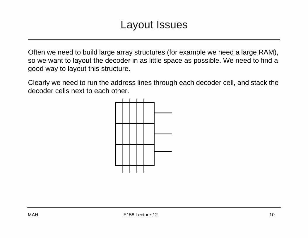
we need a large RAM), ible. We need to find a
oder cell, and stack the
MAH E158 Lecture 12
Layout Issues
Often we need to build large array structures (for example so we want to layout the decoder in as little space as possgood way to layout this structure.
Clearly we need to run the address lines through each decdecoder cells next to each other.

11
s lines.
rter buffer as the
left of the address
MAH E158 Lecture 12
Predecode Layout
The output of the predecode gate need to drive the addres
• These address lines are usually high capacitance
So usually it is better to use a NAND with an invepredecode cells.
• Cells can be placed on top of the address lines, or to thelines.
decode cells
predecode cells

12
MAH E158 Lecture 12Decoder Cell Layout
• Need to have n and p transistors
• Need to take up minimum space
• Want it to be easy to ‘program’ the cell
While layout is regular each cell is different
It connects to a different set of inputs
• Look at a couple of layout styles

13
sted. All of the area under the wires.
Vdd
MAH E158 Lecture 12
Decoder Layout
Cell Area is proportional to n2. Decoder area is n3.
The problem with this layout is that most of the space is waunder the wires is wasted. We should rotate the gate to fit
A2A2A1A1A0A0 Gnd

14
yout
ire contacts that are ou optimize the decode
nd
Out1
Out0
MAH E158 Lecture 12
A Slightly Better Decoder La
Better cell design (like we have talked about)
In this layout, the basic cell remains unchanged, it is the wprogrammed. This is sometimes a good idea, since it lets ycell (in this case the 3 input gate)
A2A2A1A1A0A0GVdd

15
tal.
t0
t1
ss lines in M2/Poly
MAH E158 Lecture 12
A Smaller Layout
Leave space for all the tracks in the cell
Need to program the decoder by placing transistors, or me
With predecode, you have more tracks per transistor.
A2A2A1A1A0A0
Gnd
Vdd
Ou
Ou
Addre

16
ge skew
iver
gate
e devices
MAH E158 Lecture 12
Wordline Driver
Decoder is just part of the wordline drive circuit
• Also need to qualify the wordline (AND with clock)
• Also need to buffer the signal to drive WL cap
Clock qualification can be done in the decoder
• A0 … An Phi1 - just another input to the decoder
Usually not a great idea, since this can lead to lar
Clock AND is usually done in last stage before dr
Φ1
decode_s1 wordline_q1
or use normal NAND
can be larg

17
ut not that large either. ter pitch. For many of
inimum useful space is
parallel, to reduce the
ontacts canbe shared
16λOut
MAH E158 Lecture 12
Thin Drivers
Wordline pitch of memory cell is not that tight (about 40λ), bThere are some memories (ROMs, dRAMs) with much tighthese applications you need thin gates and drivers. The m16λ
For the wordline driver, I might use two of these drivers in horizontal length (effectively fold the transistors again)
Gnd Vdd C
Decoderis here
In

18
software
e cell and its mirror
coder
coder
Pre
deco
der
Address
R/W
MAH E158 Lecture 12
Putting it Together
Floorplan for a memory
Built using Array constructs
• Decoder base is often array, with programming done by
Memory is built by arraying a cell that contains th
Column Mux
Row
Decode
Memory Array
Bit Line Precharge
De
2:1 Mux
Bit IO Bit IO&
Drv
Drv De
Φ1
Mem
Mem

19
high cap wires
ts the device size
ut gates
essor
apacitance
etal2)
llinging
MAH E158 Lecture 12
Transistor Sizing
For memories (and other structures) you end up with long
• Need to drive these large capacitors quickly, and this se
• We will look at chain of inverters first, and then think abo
Factors to consider in gate sizing:
• Need to think about the load you are driving
• Need to think about the load you present to your predec
Why transistor sizes matter when you are driving a large c
2pF (10mm of mmin
13ns fa26ns ris
4λ:2λ

20
match (why?)
ugh gates.
s
MAH E158 Lecture 12
Buffer (or Gate) Sizing
But bigger gates have bigger input capacitance too:
Clearly we need to make the predriver larger too. Is there an optimal solution? Yes, in a way
• Minimize delay of chain - for the minimum all delays will
• Equalizing delay principle applies to any critical path thro
400-p200-n
2pF
Delay = 0.3n
min
Delay = 4ns - falling8ns - rising
1 f f2 f3

21
MAH E158 Lecture 12
22
MAH E158 Lecture 12