Introduction to Arria 10 FPGAs and SoCs - pldworld.com · Agenda Optimized next generation...
96
Introduction to Arria 10 FPGAs and SoCs June 2013
Transcript of Introduction to Arria 10 FPGAs and SoCs - pldworld.com · Agenda Optimized next generation...

Introduction to Arria 10 FPGAs and SoCs
June 2013

Notes to Presenters
This deck is a complete, self-contained presentation for
introducing Arria 10 FPGAs and SoCs More detail on the Arria 10 SoC and HPS can be found in the Arria 10 SoC
customer presentation
When giving a combined Arria 10 / Stratix 10
presentation, we recommend you present the Arria 10
deck first, then present the Stratix 10 Blue Angels deck
second The beginning of the Arria 10 deck includes Intel announcement info and
tailored portfolio info
You can delete the Intel announcement information from the start of the Stratix 10 Blue Angels deck to eliminate redundancy
2

Agenda
Optimized next generation portfolio
Introduction to Altera’s expanded
20 nm mid-range FPGA and SoC family
Target applications for Arria 10 devices
Detailed look at Arria 10 features
Summary

February Altera Announcement
Altera will build next-generation,
high-performance FPGAs on
Intel’s 14 nm tri-gate process technology
Next-generation 14 nm tri-gate products
enable breakthrough levels of performance
and power efficiencies not otherwise
possible
Delivers a significant advantage for Altera’s
customers only major FPGA company
with access to 14 nm tri-gate technology
4

What Industry Observers are Saying
“In the hands of a competent
FPGA company, a two-process-
node lead could be deadly”
“With 14 nm silicon Altera will
get to leapfrog Xilinx, which will
be stuck.”
14 nm
4th
Generation
HK+MG
2nd
Generation
Tri-Gate

… And We Agree
6
"This will put us two to four years ahead of any of our
competitors"
—John Daane, Altera CEO

Extending Altera’s Tailored Approach With 14 nm
7
Today’s Portfolio
Single Node
28 nm
Next-Gen Portfolio
Multiple Nodes
14 nm, 20 nm, 55 nm
55 nm
20 nm
14 nm Tri-Gate
28LP
28HP

8
Altera’s Next-Generation Tailored Portfolio Roadmap
8
Cap
ab
ilit
ies
Time
High End, Mid Range FPGAs & SoCs
High End FPGAs & SoCs
Arria 10 FPGAs
Next-Gen Low Cost - TSMC 55 nm Flash
Stratix 10 FPGAs
Low Cost FPGAs
Tailored to deliver optimized capabilities to meet a
broad range of applications
Breakthrough performance with
14 nm Tri-Gate and architectural
innovations
Highest performance and
lowest power mid-range FPGAs
and SoCs
Non-volatile, lowest cost per
I/O CPLD and FPGA platform

Altera’s Next Generation Portfolio Goes to 10
9
High End
FPGAs
& SoCs
Intel 14 nm
Tri-Gate Process
TSMC
20 nm Process
60% faster vs. Arria V FPGAs,
15% vs. Stratix V FPGAs
40% lower power vs. Arria V FPGAs,
60% vs. Stratix V FPGAs
96 XCVRs, up to 28.05 Gbps
High-Performance
Mid Range
FPGAs & SoCs
2x performance of Stratix V FPGAs
Up to 70% lower power vs. Stratix V FPGAs
4M+ LEs, Up to 56 Gbps XCVRs
10+ TFLOPs DSP performance
Pin Migration

Altera’s 10th Generation Portfolio – 2x More
10 * Core performance versus previous generation
Up to 1 GHz
Core Performance
“All-In” with
ARM for SoC
60-70%
Lower Power
2x More
Bandwidth
Power
Bandwidth
SoC
Speed Arria 10: 28.05 Gbps Stratix 10: 56 Gbps
Power Saving Innovations
SoC across Density Range >2x more Fabric Density
Arria 10: 1.6x more than Arria V Stratix 10: 2x more than Stratix V

Arria V GX/GT Arria 10 Advantage
Density 500K LE 1,150K LE 2x
Multipliers 2,312 3,356 1.5x
Core Performance 300 MHz+ 500 MHz+ 1.6x
Transceiver Max Data
Rate 10 Gbps 28.05 Gbps 2.8x
Memory Interface 1333 Mbps 2666 Mbps 2x
Total Power* 1.0 0.6 40% Lower
Cross Migration No Yes to Stratix
10 Yes
11
A 2x Leap Forward with 10th Generation

Arria 10 to Stratix 10 Migration
12
GX 1150 GT 1150
1st & Largest Devices
1st Stratix 10 Device
F1152 / F1517 / F1932 Multiple Packages
Notes:
Preliminary and subject to change

Applications: 10th Gen Mid-Range and High-End FPGAs
13
More Power & Cost Sensitive More Bandwidth Intensive
Applications Industries Applications
Up to 100G Line Cards,
Nx100G Bridging & Aggregation
200G/400G Line Cards,
200G/400G Bridging & Aggregation
40G/100G Muxponders/Transponders, ODU 200G/400G Muxponders/Transponders, ODU
10G GPON / NGPON 100G TM, Packet Processing, NGPON-2
Remote Radio Heads, Channel & Switch Cards
High BW Remote Radio Heads Mobile Backhaul
Electro-Optical/IR Signal Intelligence
Guidance/Control High-End
Radar / Electronic Warfare / Secure Comms Radar, Electronic Warfare, Secure Comms
Pro AV / Videoconferencing High-End Broadcast Studio / Distribution
Studio Switcher / Server / Transport Headend Encoder / EdgeQAM / CMAP
Flash Cache & Cloud Computing
High- End
Acceleration & Custom Servers,
Diagnostic Imaging Acceleration, Custom Servers,
Diagnostic Imaging
Compute,
Storage & Medical
Broadcast
Defense
Wireless
Communications
Wireline
Communications
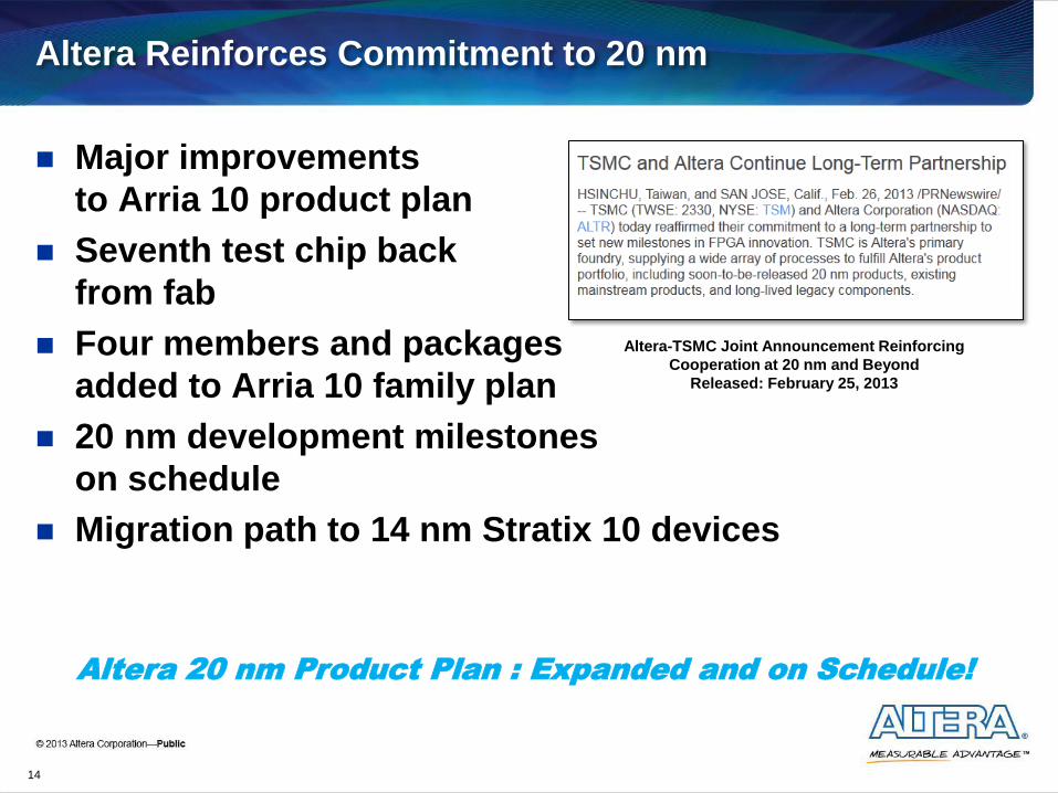
Altera Reinforces Commitment to 20 nm
Major improvements
to Arria 10 product plan
Seventh test chip back
from fab
Four members and packages
added to Arria 10 family plan
20 nm development milestones
on schedule
Migration path to 14 nm Stratix 10 devices
14
Altera-TSMC Joint Announcement Reinforcing
Cooperation at 20 nm and Beyond
Released: February 25, 2013
Altera 20 nm Product Plan : Expanded and on Schedule!

Altera 20 nm Transceiver Test Chip Lab Setup
15
Lab Setup
20 nm Test Chip Eval Board
20 nm
Test Chip

Industry’s First Transceivers @20 nm Transmit Eye at 32 Gbps
16
First Transceivers @ 20 nm Validate
28G Operation for Arria 10

17
Arria 10 FPGAs and SoCs: Reinventing the Midrange
High performance and bandwidth
Over 60% faster than prior generation
Over 15% faster than Stratix V FPGAs
Over 3.6 Tbps of transceiver bandwidth Up to 28.05G chip-to-chip, 17.4G backplane
Over 850 Gbps of DDR4 bandwidth
Over 1.2 Tbps of serial memory bandwidth
Lowest power midrange FPGAs and SOCs
Up to 60% lower power than Stratix V FPGAs, up to 40% lower than Arria V FPGAs
Comprehensive power reduction features
Highest level of integration in the midrange
Up to 1.15 million logic elements and 53 Mb embedded memory
Up to 96 transceivers
Over 3.3K 18x19 multipliers
Dual-core ARM Cortex A9 processor and subsystem
Highest Performance and Lowest Power
for Midrange Applications
Highest Performance Midrange Devices
Up to 60% Lower Power
NEW
NEW
NEW

Up to 28.05G chip-to-chip, 17.4G backplane transceivers
High-performance logic fabric
M20K embedded memory blocks
Variable-precision DSP blocks
DDR4 Support up to 2666 Mbps
PCI Express® (PCIe®) Gen1, Gen2, Gen 3
Arria 10 FPGAs and SoCs
GX
Up to 17.4 Gbps XCVRs
Up to 1.15M LEs
Up to 53 Mbits Block RAM
Up to 768 IO
GT
Up to 28.05 Gbps XCVRs
Up to 1.15M LEs
Up to 53 Mbits Block RAM
Up to 624 IO
SX
Integrated ARM Cortex-A9 Processor
Up to 17.4 Gbps XCVRs
Up to 660K LEs
Up to 42 Mbits Block RAM
Up to 624 IO NEW
28G-Capable
Family Members

Arria 10 FPGA Family Plan
19
FPGA Core Interconnects PLLs Hard IP
Device Name Logic
Elements (KLE)
M20K Blocks
M20K Bits (Mbits)
MLAB Counts
MLAB (Mbits)
18x19 Mults
Max IOs
Max XCVRs
fPLLs IO
PLLs PCIe HIPs
(x8)
GX
GX 160 160 440 9 1680 1 312 288 12 6 6 1
GX 220 220 583 11 2227 1.4 384 288 12 6 6 1
GX 270 270 750 15 3537 2.2 1600 384 24 8 8 2
GX 320 320 891 17 4673 2.9 1970 384 24 8 8 2
GX 480 480 1438 28 7137 4.4 2736 492 36 12 12 2
GX 570 570 1800 35 8241 5.0 3223 588 48 16 16 2
GX 660 660 2133 42 9345 5.7 3356 588 48 16 16 2
GX 900 900 2423 47 15080 9.2 3036 768 96 32 16 4
GX 1150 1150 2713 53 20814 12.7 3036 768 96 32 16 4
GT GT 900 900 2423 47 15080 9.2 3036 624 96 32 16 4
GT 1150 1150 2713 53 20814 12.7 3036 624 96 32 16 4
Notes:
Preliminary and subject to change
NEW Family
Members

Arria 10 GX and GT Package Plan (1 of 2)
20
Device U484 F672 F780 F1152 F1152*
Size 19x19mm 27x27mm 29x29mm 35x35mm 35x35mm 35x35mm
Package Code U19 F27 F29 F34 F35 F36
XCVR Code C (6 XCVRs) E (12 channels) E (12 channels) H (24 channels) H, K (24, 36 channels) K (36 channels)
GX FPGAs GP IO
3V IO
LVDS Pairs
XCVR GP IO
3V IO
LVDS Pairs
XCVR GP IO
3V IO
LVDS Pairs
XCVR GP IO
3V IO
LVDS Pairs
XCVR GP IO
3V IO
LVDS Pairs
XCVR GP IO
3V IO
LVDS Pairs
XCVR
GX 160 192 48 72 6 240 48 96 12 288 48 120 12
GX 220 192 48 72 6 240 48 96 12 288 48 120 12
GX 270 240 48 96 12 360 48 156 12 384 48 168 24 384 48 168 24
GX 320 240 48 96 12 360 48 156 12 384 48 168 24 384 48 168 24
GX 480 360 48 156 12 492 48 222 24 396 48 174 36
GX 570 492 48 222 24 396 48 174 36
GX 660 492 48 222 24 396 48 174 36 432 48 174 36
GX 900 528 0 264 24 432 0 216 36
GX 1150 528 0 264 24 432 0 216 36
Pin migration across
devices within family
Notes:
a) Preliminary and subject to change
b) GPIO counts include 3V IO and LVDS IO; GPIO that do not support 3V IO can support LVDS
c) Each LVDS pair can be configured as either a differential input or as a differential output
d) Up to 48 GPIO pins may be used for programming
e) All packages are 1.0mm ball pitch except U484 which is 0.8mm ball pitch
f) Packages of similar footprint (ie, the two F1152 columns shown in table above) may have different package form factors. Please consult package outlines.
*These packages will each have two different package outlines
NEW NEW
Pin Migration to Stratix 10 Devices

Arria 10 GX and GT Package Plan (2 of 2)
21
Device F1517* F1517 F1932 F1932 F1932
Size 40x40mm 40x40mm 45x45mm 45x45mm 45x45mm
Package Code F40 F40 F45 F45 F45
XCVR Code N (48 channels) R (66 channels) N (48 channels) S (72 channels) U (96 channels)
GX FPGAs GPIO 3V IO LVDS Pairs
XCVR GPIO 3V IO LVDS Pairs
XCVR GPIO 3V IO LVDS Pairs
XCVR GPIO 3V IO LVDS Pairs
XCVR GPIO 3V IO LVDS Pairs
XCVR
GX 570 588 48 270 48
GX 660 588 48 270 48
GX 900 624 0 312 48 342 0 154 66 768 0 384 48 624 0 312 72 480 0 240 96
GX 1150 624 0 312 48 342 0 154 66 768 0 384 48 624 0 312 72 480 0 240 96
GT FPGAs
GT 900 624 0 312 48 624 0 312 72 480 0 240 96
GT 1150 624 0 312 48 624 0 312 72 480 0 240 96
Pin migration across
devices within family
NEW NEW
Notes:
a) Preliminary and subject to change
b) GPIO counts include 3V IO and LVDS IO; GPIO that do not support 3V IO can support LVDS
c) Each LVDS pair can be configured as either a differential input or as a differential output
d) Up to 48 GPIO pins may be used for programming
e) All packages are 1.0mm ball pitch except U484 which is 0.8mm ball pitch
f) Packages of similar footprint (ie, the two F1517 columns shown in table above) may have different package form factors. Please consult package outlines.
*This packages will have two different package outlines
Pin Migration to Stratix 10 Devices

Arria 10 SoC Family Plan
22
LOGIC CORE Interconnects PLLs Hard IP
Device Name Logic
Elements (KLE)
M20K Blocks
M20K Bits (Mbits)
MLAB Counts
MLAB (Mbits)
18x19 Mults
Max IOs
Max XCVRs
fPLLs IO
PLLs PCIe HIPs
(x8)
Arr
ia 1
0 S
X S
oC
SX 160 160 440 9 1680 1 312 288 12 6 6 1
SX 220 220 583 11 2227 1.4 384 288 12 6 6 1
SX 270 270 750 15 3537 2.2 1600 384 24 8 8 2
SX 320 320 891 17 4673 2.9 1970 384 24 8 8 2
SX 480 480 1438 28 7137 4.4 2736 492 36 12 12 2
SX 570 570 1800 35 8241 5.0 3223 588 48 16 16 2
SX 660 660 2133 42 9345 5.7 3356 588 48 16 16 2
Notes:
Preliminary and subject to change

Arria 10 SoC Package Plan: Small Form Factor (1 of 2)
23
Device U484 F672 F780
Size 19x19mm 27x27mm 29x29mm Package Code U19 F27 F29
XCVR Code C (6 XCVRs) E (12 channels) E (12 channels)
SoC GP IO
3V IO
LVDS Pairs
XCVR GP IO
3V IO
LVDS Pairs
XCVR GP IO
3V IO
LVDS Pairs
XCVR
SX 160 192 48 72 6 240 48 96 12 288 48 120 12
SX 220 192 48 72 6 240 48 96 12 288 48 120 12
SX 270 240 48 96 12 360 48 156 12
SX 320 240 48 96 12 360 48 156 12
SX 480 360 48 156 12
SX 570
SX 660
Pin migration across
devices within family
Notes:
(1) All packages are ball grid arrays with 1.0mm pitch, except for U19 (U484) which is 0.8mm pitch.
(2) High-Voltage I/O pins are used for 3.3V and 2.5V interfacing.
(3) Each LVDS pair can be configured either as a differential input, or as a differential output.
(4) High-Voltage I/O pins and LVDS Pairs are included in the General Purpose I/O count. Transceivers are counted
separately.
(5) Each package column offers pin migration (common circuit board footprint) for all devices in the column.
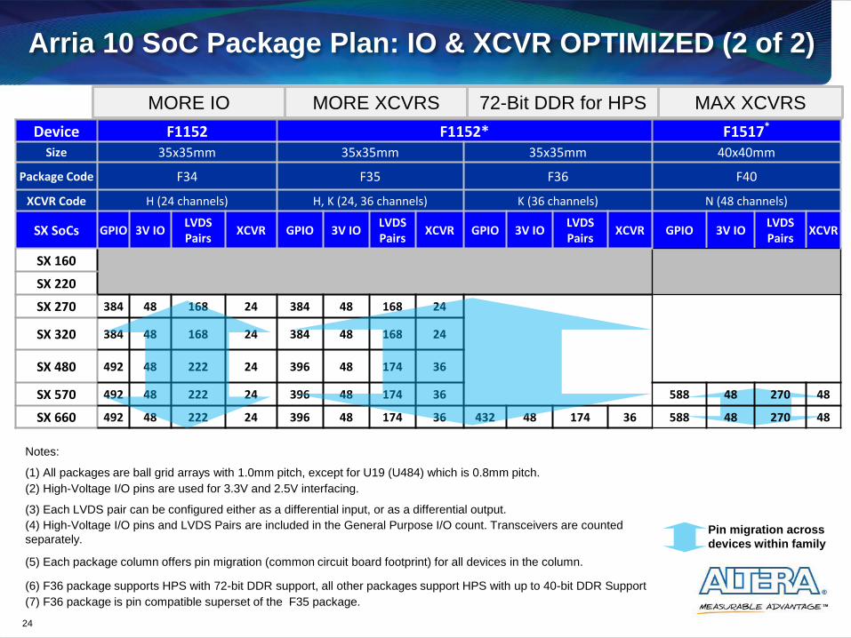
Arria 10 SoC Package Plan: IO & XCVR OPTIMIZED (2 of 2)
24
Pin migration across
devices within family
Device F1152 F1152* F1517* Size 35x35mm 35x35mm 35x35mm 40x40mm
Package Code F34 F35 F36 F40
XCVR Code H (24 channels) H, K (24, 36 channels) K (36 channels) N (48 channels)
SX SoCs GPIO 3V IO LVDS Pairs
XCVR GPIO 3V IO LVDS Pairs
XCVR GPIO 3V IO LVDS Pairs
XCVR GPIO 3V IO LVDS Pairs
XCVR
SX 160
SX 220
SX 270 384 48 168 24 384 48 168 24
SX 320 384 48 168 24 384 48 168 24
SX 480 492 48 222 24 396 48 174 36
SX 570 492 48 222 24 396 48 174 36 588 48 270 48
SX 660 492 48 222 24 396 48 174 36 432 48 174 36 588 48 270 48
MORE IO MORE XCVRS 72-Bit DDR for HPS
Notes:
(1) All packages are ball grid arrays with 1.0mm pitch, except for U19 (U484) which is 0.8mm pitch.
(2) High-Voltage I/O pins are used for 3.3V and 2.5V interfacing.
(3) Each LVDS pair can be configured either as a differential input, or as a differential output.
(4) High-Voltage I/O pins and LVDS Pairs are included in the General Purpose I/O count. Transceivers are counted
separately.
(5) Each package column offers pin migration (common circuit board footprint) for all devices in the column.
(6) F36 package supports HPS with 72-bit DDR support, all other packages support HPS with up to 40-bit DDR Support
(7) F36 package is pin compatible superset of the F35 package.
MAX XCVRS

Arria 10 Compared to Stratix V

Arria 10 Compared to Stratix V
26
Feature Stratix V Arria 10
Process TSMC 28HP TSMC 20SoC
Power/
Performance
Core Performance Baseline 15%+ Faster than Stratix V
Power Baseline Up to 60% lower
Core Resources
Density 952 KLE 1.15M LE
Embedded Memory 52Mbit + 53Mbit +
DSP 3,926 18x18 Multipliers 3,356 18x19 Multipliers
XCVR Capability
Channel Count 66 96
Backplane 14.1 Gbps 17.4 Gbps
Chip-to-Chip 28.05 Gbps 28.05 Gbps
IO/ External
Memory IF
Parallel Memory DDR3 @ 1866Mbps DDR4 @ 2666Mbps
Serial Memory Evaluation Over 1.2 Tbps
PCI Express Gen3 x8 Gen3 x8
Additional
Integration
Hard Processor - Dual Core ARM A9
Memory Controller Soft Hard
Attractive Migration from Stratix V to Lower
Power Midrange Arria 10 Devices

Select Arria 10 Target Applications

10
0G
E
OT
U4
OTL4.10
Line
Side
OTU
Framer
Arria 10 Applications Example: OTN 100G Transponder
28
Stratix V Arria 10 Improvement
Power 31.4W 18.9W 40%
Arria 10 FPGA Delivers 40% Power Reduction
vs. Prior Generation
100GE
– ODU4
Mapper
CAUI
10
0G
E
OT
U4
OTL4.10
Line
Side
OTU
Framer
100GE
– ODU4
Mapper
CAUI
Design Details
FPGA Core
490 KLE
2.6 Mbits RAM
260 MHz main clock
IO Interfaces
20 XCVRs @ 11.18 Gbps
20 XCVRs @ 11.3 Gbps
2 XCVRs @ 2.5 Gbps
Arria 10 Product Advantages
Robust protocol support for OTU4, GE
Low power transceivers
XCVR support up to 28.05 Gbps
Comprehensive power reduction
feature set
Conditions: 100C Max

Arria 10 Applications Example: Mobile Backhaul
29
ARM HPS Sub-System
ARM Core
GP
IO &
XC
VR
s G
PIO
& X
CV
RS
MultiPort DDR SDRAM Controller PCIe
ARM Core
L2 Cache
DMA
GPIO
Ethernet NAND JTAG
Snoop Control (SCU)
Pa
ck
et
Inte
rfa
ce
Eth
Eth
Eth
Eth
PseudoWire
Tx
Eth
Eth
Eth
Eth
PseudoWire
Rx
Pa
ck
et In
terfa
ce
1588
Subsystem
OAM
Subsystem
Packet
Process
Packet
Update
Traffic
Manager
FPGA Cfg Multiport DDR
SDRAM Controller HPS
to
FPGA
Buffer
Design Details
FPGA Core
400 KLE
12.3 Mbits RAM
500 18x18 mults
250 Mhz main clock
IO Interfaces
8 XCVRs @ 10.3 Gbps
3x DDR3 x32 @533 Mhz
Arria 10 Product Advantages
Flexibility vs. ASSP solutions
Single-chip integration of processor
and external switch to reduce power
and space
In-field upgradability
Comprehensive power reduction
feature set
Arria V + CPU +
Switch
Arria 10
SoC Improvement
Power 26.2W 13.7W 47.7%
Conditions: 100C Max
Lowest Power Single-Chip Implementation Supporting
In-Field Hardware Upgrades

Arria 10 Applications Example: 100G Traffic Manager
30
Eth
ern
et
Inte
rfac
e
QDRII+ Memory Interface
Queue
Management
Packet Buffer
Scheduler Shaper
Linked Lists/
Descriptor
Tables
HMC Serial Memory
Interface
Inte
rla
ke
n B
ac
kp
lan
e
Inte
rfac
e
Ethernet MAC
and PHY
Stratix V Arria 10 Improvement
Performance 272MHz 315MHz 15.8%
Power 50.4W 40.5W 19.6%
Performance Increase of 15%+ AND ~20% Power Reduction
Design Details
FPGA Core
875 KLE
25 Mbits RAM
IO Interfaces
12 XCVRs @ 12.5 Gbps
30 XCVRs @ 11.3 Gbps
10 XCVRs @ 10.3 Gbps
6x QDRII+ x36
@500 MHz
Arria 10 Product Advantages
Backplane support up to 17.4 Gbps
Hard 10G/40G-Base KR FEC
Industry-leading HMC support
Robust protocol support for Interlaken
& GE
Low power transceivers
Conditions: 100C Max

Arria 10 Applications Example: Broadcast UDX
31
n Deinterlace,
Scale,
Color,
Correction
n Mixer
Switch
Input
Connectivity
SDI
GigE
Production
Outputs
Monitor
Outputs
DDR Multi-Port
Front End
SDI
GigE
HDMI
DisplayPort
Design Details
FPGA Core
250 KLE
14.7 Mbits RAM
60 18x18 mults
200 Mhz main clock
IO Interfaces
8 XCVRs @ 3 Gbps
4 XCVRs @ 5.4 Gbps
2x DDR3x72 @533 Mhz
Arria 10 Product Advantages
DDR4 support up to 2.6 Gbps
Protocol support for SDI, DisplayPort,
HDMI & GE
RAM widths optimized for video data
Up to 96 XCVR channels for scalable
switching
Stratix V Arria 10 Improvement
Power 14.2W 8.5W 40%
Conditions: 100C Max
Lowest Power Single-Chip Implementation for Wide Variety
Of Switching Applications

Arria 10 Applications Example: 2x2 Remote Radio Head
32
ARM HPS Sub-System
Fra
me
r
ARM Core
Digital
Upconversion
Eth
ern
et
Data
Co
nve
rsio
n
DD
R3 In
terfa
ce
C
PR
I/OB
SA
I
ARM Core
Host Debug Interface DDR3 Interface
CFR CFR
Digital
Downconversion
Design Details
FPGA Core
260 KLE
30 Mbits RAM
1508 mults
IO Interfaces
2 XCVRs @ 9.8 Gbps
10 XCVRs @ 6.144 Gbps (Rx)
2 XCVRs @ 6.144 Gbps (Tx)
2x DDR3x72 @533 Mhz
Arria 10 Product Advantages
Lowest-power implementation of all
RRH digital functions
Protocol support for CPRI, OBSAI
Comprehensive power reduction
feature set
Stratix V Arria 10 Improvement
Performance 368MHz 491MHz 33.4%
Power 26.4W 17.7W 35%
Arria 10 Achieves <20W Thermal Limit for 491 MHz Radio Heads

Arria 10 Performance and Power

Arria 10 FPGAs: Highest Performance 20 nm FPGAs
Over a speed grade faster than
prior generation high-end FPGAs 15%+ faster than Stratix V FPGAs
60%+ faster than Arria V GX/GT FPGAs
Over 500 MHz at industrial temperatures
1.7x faster embedded RAM
1.6x faster multiplications
Embedded ARM Cortex A9 dual-
core processor at 1.5 GHz Over 1.8x faster than Altera’s 28 nm
SoC devices
34
(Average result from benchmark suite)
I3, C
3 (
Fa
ste
st)
(C
om
me
rcia
l/In
dustr
ial gra
de
s)
Co
re P
erfo
rman
ce
I3
(F
as
tes
t)
Ind
ustr
ial gra
de
Arria V
GZ
1.0
1.30x
Arr
ia 1
0 G
X/S
X (
Fa
ste
st)
(C
om
me
rcia
l/In
dustr
ial gra
de
s)
1.62x+
Arria 10
GX/GT Arria V
GX/GT Arria 10 FPGAs & SoCs:
Built for Performance
C2
–C
4, I2
-I4
(Co
mm
erc
ial/In
dustr
ial gra
de
s)
1.45x
Stratix V
Over a speed
grade faster than
Stratix V

Arria 10 FPGAs & SoCs: Lowest Power @ 20 nm
Advanced 20 nm process
Comprehensive power reduction features
Lowest transceiver power in class
Reduced static power options
Most power-efficient embedded processor
Extensive use of hard IP
35
Up to 40% Lower Power than Prior Generation
Midrange FPGAs
36
Power Reduction in Arria 10 vs. Arria V
Up to 35%
To
tal
Po
wer
(No
rma
lize
d t
o A
rria
V F
PG
A P
ow
er)
Arria V GX/GT
FPGAs
Arria 10 Devices
(Process, IC Optimization,
Architecture, Hard IP, Lower Vcc)
Up to 40%
Up to 45%
Up to 15%
Arria 10 Devices
with Power Reduction
Techniques
(User Options)
Up to 40%
Lower
Total
Power
Up to 15%
Lower
Total
Power
Up to 40% Total Power Reduction Compared
to Arria V GX/GT FPGAs
Up to 65%

37
Power Reduction in Arria 10 vs. Stratix V
Up to 20%
Up to 35%
To
tal
Po
wer
(No
rma
lize
d t
o S
tra
tix
V F
PG
A P
ow
er)
Stratix V FPGAs
(standard power)
Arria 10 Devices
(Process, IC Optimization,
Architecture)
Up to 55%
Up to 35%
Up to 60%
Up to 15%
Arria 10 Devices
with Power Reduction
Enhancements (User Options)
Up to 60%
Lower
Total
Power
Up to 35%
Lower
Total
Power
Up to 60% Total Power Reduction Compared
to Stratix V FPGAs

Arria 10 Transceiver Power Reduction
38
0
50
100
150
200
250
300
3G 6G 10G 12.5G 17G
Arria V GX/GT
Arria 10
Up to 40% Power Reduction Per Channel Compared
to Prior Generation
mW
Pe
r C
han
ne
l
Conditions: 85°C Junction Maximum Power
Line rates not possible
in Arria V GX/GT

39
Arria 10 Power Saving Innovations
Vcc
PowerManager
Programmable
Power
Technology
Enables device to run at lower than nominal Vcc
while retaining same performance level reducing
static and dynamic power
Low Static
Power Speed
Grades
Enables lower power transistors for non-
performance critical paths to reduce static power
Lower operating Vcc to trade off performance
to achieve lower total power
Devices tested to lower static power and
designated -L (low static power)
SmartVoltage ID

SmartVoltage ID Power Reduction
Allows FPGA to be operated at lower core Vcc while retaining same performance
Reduces static power and also average dynamic power consumption across distribution of devices Lower OpEx
Requires power system controller that can support tuned voltage
40
Reduce Static Power by Up to 40%
Arria 10 FPGA
Host Power System
Controller
Option 2 Option 1
Tuned
Vcc
Voltage
Vcc
SmartVoltage ID

SmartVoltage ID Power Reduction Details
41
Devices that are higher static
power than SmartVoltage ID
power limit
Standard Device Static Power Limit (max shown in EPE)
Sta
tic
Po
we
r
Static power distribution
across devices
Can Run These Devices At Lower Voltage
(SmartVoltage ID) and Still Meet Performance Guaranteed Static Power
Savings Relative to Worst-
Case Standard Devices
SmartVoltage ID Static Power Limit (will be shown in Arria 10 EPE)

Programmable Power Technology
42
Accelerate speed-critical
paths while reducing
power on non-speed
critical paths
Quartus II optimizes your design
automatically, enabling high-speed
logic only where needed
Get performance where you
need it, and reduced power
everywhere else
Static
Power
Threshold Voltage
Patented Altera Technology Reduces Core
Static Power by Up to 20%

Vcc PowerManager in Arria 10 FPGAs
Use lower Vcc to achieve
lower power by trading
off performance
When lower Vcc applied,
Fast speed grade devices
operate at slower speed
Requires timing closure
at slower core speed
43
Device Speed Grade
Applied
Vcc
Level
Fast Mid Slow
Standard
Vcc
Fast
core
speed
Mid
core
speed
Slow
core
speed
Lower
Vcc
Slow
core
speed
NA
Reduces Total Power by Up to 35%

Lower Static Power Speed Grades
Takes advantage of
process variation to
offer lower static
power devices (-L)
Offered for both Extended
(0ºC – 100ºC) and Industrial
(-40ºC – 100ºC) versions
44
Reduce Static Power by Up to 25%
Higher leakage, higher static power
Lower leakage, lower static power
Distribution of Semiconductor Devices
Dis
trib
uti
on
Performance
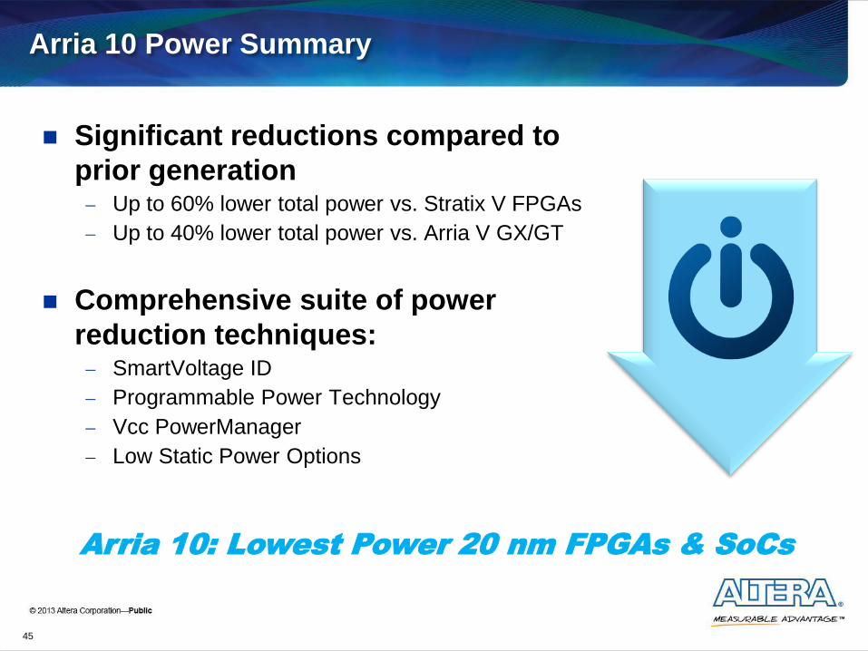
Arria 10 Power Summary
Significant reductions compared to
prior generation Up to 60% lower total power vs. Stratix V FPGAs
Up to 40% lower total power vs. Arria V GX/GT
Comprehensive suite of power
reduction techniques: SmartVoltage ID
Programmable Power Technology
Vcc PowerManager
Low Static Power Options
45
Arria 10: Lowest Power 20 nm FPGAs & SoCs

Transceivers

47
Arria 10 Transceivers
Planned Protocol Support
10G-Base R/KR PCI Express Gen 3
CEI-6G/10G Infiniband
CPRI QPI
DisplayPort SATA / SAS
FibreChannel SDI – SD/HD/3G/10G
GPON Serial RapidIO
Gigabit Ethernet
(GbE) SFP + / XFP
Higig+ SFI – 4.2 / 5.2
IEEE 802.3ba 40G /
100G SGMII
Interlaken SONET OC-192
JESD204B XAUI
OTU – 2/3/4
Custom protocols
supported using
“Native PHY” mode
NEW
NEW
NEW
NEW
Highest bandwidth in a midrange FPGA
Over 3.6 Tbps of transceiver bandwidth
Up to 96 XCVRs
Up to 28.05G chip-to-chip/chip-to-module
Backplane support up to @17.4G
First midrange FPGAs with >12G backplane support
Hard Nios II processor for individual transceiver tuning and
better signal integrity
Hard IP for 10G/40GBase-KR FEC
Industry’s strongest transceiver pedigree
Comprehensive transceiver IP portfolio
developed over a decade
Across ten product generations
Overseen by the same core
development team
Leveraging over 100
man years of field-
tested expertise

Arria 10 Protocol Support
48
Market Segment Standards Protocol / Data rate
Wireline
IEEE
GbE (1.25Gbps) XAUI, HiGig (>3.75G) 10GBase-R, 10GBase-KR, 40GBase-KR4, 40GE, 100GE XLAUI (4x10G), CAUI (10x10G) CAUI-4, CPPI-4 1588, SyncE, low latency
Interlaken 6.25/10.3125/11.3/28G
OIF CEI 6G-SR/LR, 11G-SR/LR, 25G-SR/VSR, 28G-SR/VSR SFI-S 10G/28G, SFI-5.1/5.2 (17x3.125G, 4x10G)
ITU SONET OC-3/12/48/192/768 (0.155, 0.622, 2.488, 9.95, 4x10G) OTU-1/2/3 (2.66, 10.7, 4x10.7G, 4x25G) OTL 3.4/4.4/4.10/5.16 (4x10G, 4x25G, 10x10G, 16x25G)
GPON/EPON 1.25/2.5/10G
Military/Wireless JEDEC JESD204B (3, 6.25, 12.5G)
SRIO 1.25/2.5/3.125/6/10G
Wireless CPRI 0.6144, 1.2288, 2.4576, 3.072, 4.9152, 6.144, 9.83, 10.13, 12.67, 20G
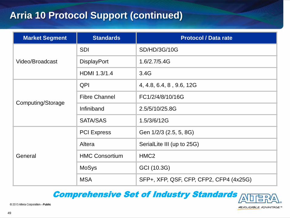
Arria 10 Protocol Support (continued)
49
Market Segment Standards Protocol / Data rate
Video/Broadcast
SDI SD/HD/3G/10G
DisplayPort 1.6/2.7/5.4G
HDMI 1.3/1.4 3.4G
Computing/Storage
QPI 4, 4.8, 6.4, 8 , 9.6, 12G
Fibre Channel FC1/2/4/8/10/16G
Infiniband 2.5/5/10/25.8G
SATA/SAS 1.5/3/6/12G
General
PCI Express Gen 1/2/3 (2.5, 5, 8G)
Altera SerialLite III (up to 25G)
HMC Consortium HMC2
MoSys GCI (10.3G)
MSA SFP+, XFP, QSF, CFP, CFP2, CFP4 (4x25G)
Comprehensive Set of Industry Standards

Arria 10 Transceiver Enhancements
Feature Arria V GX/GT Arria V GZ Arria 10 Devices
Technology 28 nm 28 nm 20 nm
Transceivers 32 36 96
Data Rate 6.5Gbps
/10.3125Gbps
12.5Gbps chip-to-chip
12.5Gbps backplane
28.05Gbps
chip-to-chip
17.4Gbps backplane
Transmit
Pre-emphasis Yes Yes Yes
Adaptive CTLE
(Continuous Time
Linear Equalizer)
Yes Yes Yes
Adaptive DFE
(Decision Feedback
Equalizer)
No Yes Yes
Backplane Total
Equalization Gain No 25dB >30dB
50
Arria 10 Delivers High-End
Transceiver Performance

Arria 10 Transceiver Overview
51
High Port Count and High Bandwidth Applications in a
Mid-range platform
Arria 10 GX Arria 10 GT
Transceiver Count Up to 96 Up to 96
Max Data Rate 17.4 Gbps 28.05 Gbps
Number of 28G Channels 0 16
Max Backplane Data Rate 16 Gbps 17.4 Gbps
XCVR
x6
XCVR
x6
XCVR
x6
XCVR
x6
XCVR
x6
XCVR
x6
XCVR
x6
XCVR
x6
XCVR
x6
XCVR
x6
XCVR
x6
XCVR
x6
XCVR
x6
XCVR
x6
XCVR
x6
XCVR
x6
XCVR
x6
XCVR
x6
XCVR
x6
XCVR
x6
XCVR
x6
XCVR
x6
XCVR
x6
XCVR
x6
XCVR
x6
XCVR
x6
XCVR
x6
XCVR
x6
XCVR
x6
XCVR
x6
XCVR
x6
XCVR
x6
28.05 Gbps
Capable
Channels
GX GT

Arria 10 GT Backplane Support At 17.4Gbps
52
12.5-17.4Gbps backplane data rate
(6.25-8.7GHz fundamental frequency)
Example: Backplane Insertion Loss: 29.8” = 17” BP + ~12” (2 connectors + 2 paddle cards)
42.8” = 30” BP + ~12” (2 connectors + 2 paddle cards)
Source: TE Connectivity Strada Whisper
Backplane Channels Presentation 4/29/11
Arria 10 optimal
equalization range
up to 17.4Gbps
backplane
First
Midrange
FPGA to
Support 17G
Backplanes

Arria 10 FPGA On-Die Instrumentation
View eye-opening at CDR input, inside receiver Complete X and Y reconstruction of post-equalized eye opening
Evaluate effectiveness of signal-conditioning techniques Verify optimal pre-emphasis, CTLE, and DFE settings for largest eye opening
2X horizontal and 2X vertical resolution compared to Arria V GZ
53
Minimize Board Bring up / Debug Time
With EyeQ
Transmitter Output Receiver Input Lossy Channel
Pre-
Emphasis EQ CDR
EyeQ™
Captured with
Oscilloscope
Captured with
Oscilloscope
Captured with
Transceiver Toolkit
Horizontal: 64-slice
Vertical: 128-slice

Arria 10 Protocol Specific Hard IP
54
Hard IP Included Features
PCIe Gen3 x8 PCI Express compliant PHY, PCS, data link and transaction layers with
bypass options
Interlaken Gearbox/bit slip, block synchronization, disparity generator/checker,
scrambler/descrambler, frame synchronization, CRC-32
generator/checker, frame generator and TX/RX FIFO
10GBASE-R Gearbox/bit slip, block synchronization, scrambler/descrambler,
64b/66b encoder/decoder and TX/RX FIFO
10GBASE-KR
40GBASE-KR4
Gearbox/bit slip, block synchronization, KR FEC (new),
scrambler/descrambler, 64b/66b encoder/decoder and TX/RX FIFO
(with auto-negotiation and link training supported in soft IP)
Basic 8b/10b Word aligner and bit slip, rate match FIFO, 8B/10B encoder/decoder,
byte serializer, de-serializer, byte ordering and phase compensation
FIFO
Basic 64b/66b Gearbox/bit slip, block synchronization, scrambler/descrambler,
64b/66b encoder/decoder and TX/RX FIFO
Increased Productivity with Maximum Performance
and Power Efficiency
55
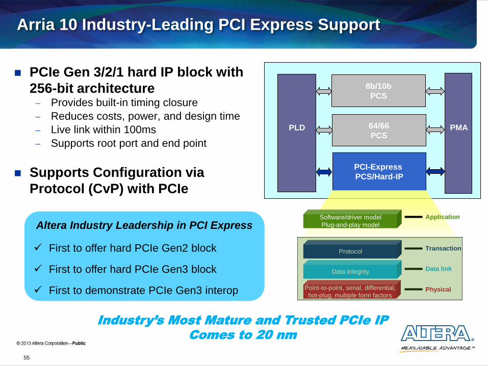
Arria 10 Industry-Leading PCI Express Support
PCIe Gen 3/2/1 hard IP block with
256-bit architecture Provides built-in timing closure
Reduces costs, power, and design time
Live link within 100ms
Supports root port and end point
Supports Configuration via
Protocol (CvP) with PCIe
Altera Industry Leadership in PCI Express
First to offer hard PCIe Gen2 block
First to offer hard PCIe Gen3 block
First to demonstrate PCIe Gen3 interop
8b/10b
PCS
PLD 64/66
PCS
PCI-Express
PCS/Hard-IP
PMA
Point-to-point, serial, differential,
hot-plug, multiple form factors
Data integrity
Protocol
Software/driver model
Plug-and-play model
Application
Transaction
Data link
Physical
Industry’s Most Mature and Trusted PCIe IP
Comes to 20 nm

Parallel and Serial Memory Interfaces
Arria 10 FPGA
57
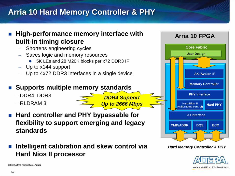
Arria 10 Hard Memory Controller & PHY
High-performance memory interface with
built-in timing closure Shortens engineering cycles
Saves logic and memory resources 5K LEs and 28 M20K blocks per x72 DDR3 IF
Up to x144 support
Up to 4x72 DDR3 interfaces in a single device
Supports multiple memory standards DDR4, DDR3
RLDRAM 3
Hard controller and PHY bypassable for
flexibility to support emerging and legacy
standards
Intelligent calibration and skew control via
Hard Nios II processor
Core Fabric
User Design
ECC
I/O Interface
Hard PHY
PHY Interface
Memory Controller
Hard Memory Controller & PHY
AXI/Avalon IF
DQS CMD/ADDR
DDR4 Support
Up to 2666 Mbps Hard Nios II
(calibration/ control)

58
Feature Arria V GX/GT Arria 10
Interfaces Supported DDR3, DDR2 DDR4, DDR3
RLDRAM III
Maximum Interface Width x64 x144
Maximum Interface Rate 1066 Mbps (DDR3) 2133 Mbps (DDR3)
2666 Mbps (DDR4)
Maximum x32 I/F per Device 4 7
DIMM Support None DDR4, DDR3
Arria 10 Hard Memory Controller Enhancements
Higher Performance and Greater Capability
Compared to Prior Generation
400
500
600
700
800
900
1000
1100
1200
1300
1400
DDR4 DDR3 RLDRAM 3 RLDRAM 2 QDR IV QDR II+
FastMediumSlow
59
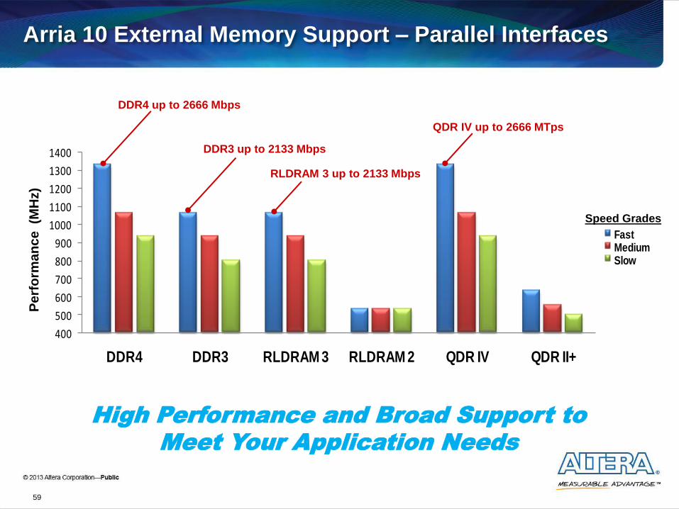
Arria 10 External Memory Support – Parallel Interfaces P
erf
orm
an
ce
(M
Hz)
DDR4 up to 2666 Mbps
High Performance and Broad Support to
Meet Your Application Needs
RLDRAM 3 up to 2133 Mbps
QDR IV up to 2666 MTps
Speed Grades
DDR3 up to 2133 Mbps

Hybrid Memory Cube (HMC) Technology
60
HMC technology basics Ultra high performance, multi-bank DRAM memory
DRAM die stacked using state-of-the-art 3D process
Built-in memory controller with logic base die
Unparalleled gains with HMC Maximum DRAM bandwidth of up to 160 GB/s
Four links running at 15 Gbps offering nearly 1 T bps raw interface bandwidth
Up to 4GB density (storage) capacity, low PHY power (pj/bit)
Best in class RAS feature set
Parameters Specification
Link 4
Speed 10,12.5,15 Gbps
Density 2GB, 4GB
Vaults 16
Banks 128, 256
DRAM B/W 160 GB/s (1.2 Tbps)
Vault B/W 10 GB/s (80 Gb/s)

Altera Technology Leadership in HMC
61
HMC interoperability demo planned mid 2013 First interoperability with HMC
Lead development platform to fully test and validate Altera HMC performance
Altera support for HMC technology Arria 10 and Stratix 10 FPGAs and SoCs
Up to 4 links (16 lanes per link) @ 10G ,12.5G, 15G
Logic Base Die
High-Speed Link,
64 Total Serial channels Wide Data Path
Altera FPGA
DRAM Die
Industry’s First Support for HMC

Arria 10 Memory Interface Support by Speed Grade
Memory Standards
Extended & Industrial (MHz)
-2 Grade -3 Grade -4 Grade
Parallel Memory
1 Rank
/ CS
2 Rank /
CS
1 Rank /
CS
2 Rank
/ CS
1 Rank /
CS
2 Rank /
CS
DDR4 UDIMM/RDIMM/Comp 1333 1200 1200 1066 1066 933
DDR4 LRDIMM 1333 1333 1333 1200 1066 1066
DDR3 / 3L 1066 933 1066 933 933 800
QDR IV 1333 1066 1066 933 933 800
QDR II+ / DDR II+ Extreme 633 633 550 550 500 500
RLDRAM 3 1200 1066 1066 933 933 800
RLDRAM 2 533 533 533 533 533 533
LPDDR3 800 800 800 800 667 667
Serial Memory
Hybrid Memory Cube (HMC) 16x15 Gbps per link, up to 4 links
62
Full Support for Key Parallel and
Serial Memory Interfaces

Variable Precision DSP Block

64
Extending an Award-Winning DSP Architecture
Industry’s First Variable-Precision DSP Block Winner: DesignVision 2011 Award
Introduced at 28 nm generation – exclusive to Altera
Refined and improved at 20 nm
Expanded with new capabilities for high performance

Combines the Best of Stratix V & Arria V
65
Hard Pre-Adders
Reduce multiplier usage
Save routing resources
Integrated Coefficient Registers
Save memory and routing
resources
Built-in timing closure
Multiplier Modes for Flexibility
Two 18x19 multipliers, or
One 27x27 multiplier per block
36x36, 54x54 modes using
multiple DSP blocks
64-bit Cascade Path
Supports systolic FIR
Sum of products
Up to 64-bit Adder/
Subtractor/Accumulator
1,024-tap filters
2,048-tap symmetric filters
Feedback Register and
Multiplexer
Implement two independent
filter channels per DSP block
Efficient Fixed Point FIR Filter and
FFT Implementation
Introduced for Arria V
FPGAs, standard for all
20 nm FPGAs
Serial FIR Direct FIR Systolic FIR

Arria 10 Core Fabric

67
Arria 10 M20K Block Feature Summary
Feature Arria V Arria 10
Maximum Performance 380 MHz 730 MHz
Total RAM Bits per Block 10,240 20,480
Total M20K Memory Bits (Mb) per Device 8-24 13-54
Port Width Configurations
8K x1, 4K x2
2K x 4, 5
1K x 8, 10
512 x 16, 20
256 x 32, 40
16K x 1, 8K x 2
4K x 4, 5
2K x 8, 10
1K x 16, 20
512 x 32, 40
Parity
Byte Enable
Packed Mode
Address Clock Enable
Mixed Clock
Mixed Width (for Dual Port modes)
ECC Support Soft Hard
Memory Modes
Single Port
Simple & True Dual-Port
Shift Register, ROM, FIFO
Higher Performance, More Port Configurations,
and Hard ECC

68
Arria 10 MLAB Feature Summary
Feature Arria V Arria 10
Maximum Performance 300 MHz 700 MHz
Total RAM Bits per Block 640 640
Total Memory Bits (Mb) per Device 0.4 – 2.9 2-13
Port Width Configurations
32 x 16
32 x 18
32 x 20
32 x 16
32 x 18
32 x 20
Parity
Byte Enable
Address Clock Enable
Mixed Clock
Mixed Width (for Dual Port modes)
ECC Support
Memory Modes
Single Port*
Simple Dual-Port
Shift Register, ROM, FIFO
x 64 deep mode
supported in
emulation mode
Over 2X Performance Increase Compared
to Prior Generation

Core PLLs
IO PLLs
Feature Description
Number available 1 for every IO bank (48 GPIOs)
Location on die In the core, adjacent to IO banks
Operating modes Integer (M/N where M,N = Integer)
FPGA clock
network access
External Memory Interface
LVDS SerDes Interface
GCLK (global clock)
PCLK (periphery clock)
RCLK (regional clock)
69
Delta
Sigma
Modulator
fIN
fVCOfPFD
fOUTDivide
by C
Phase
Frequency
Detect
Charge
Pump
Low
Pass
Filter
VCODivide
by N
Divide
by M
FractionΣ
fIN
fVCOfPFD
fOUTDivide
by C
Phase
Frequency
Detect
Charge
Pump
Low
Pass
Filter
VCODivide
by N
Divide
by M
Fractional PLLs
Feature Description
Number available 1 for every 3 transceivers on device
Location on die In the core, adjacent to transceivers
Operating modes Fractional-synthesis
Integer (M/N where M,N = Integer)
FPGA clock
network access
Transceiver reference clock
GCLK (global clock)
PCLK (periphery clock)
RCLK (regional clock)
fPLLs Reduce Cost, Power and
Circuit Board Space
IO PLLs Enable High-Bandwidth
IO Interfaces
More PLLs, Optimized For Transceivers
and IOs

70
Configuration Via Protocol Using PCIe
Full PCIe Gen3 x8 loading capability
Low pin count, fast configuration
3,000 Mbps vs. 30 Mbps via serial EPCS device configuration
Greater flexibility for configuration storage
Support of partial reconfiguration
Flexible, Low Pin Count Configuration
Compliant with PCI-SIG®
PCIe Link
CPU or Host
Configuration
20 nm
NEW!

Software and Tools

Requires More Than Just the Silicon
72
ARM Ecosystem Qsys System Integration Tool
Software Programming Support
Video and
Image
Processing OTN
Memory
Controllers
Floating
Point
Open standard for
cross-platform design (µP, DSP, GPU)
DSP
Builder
Enabling Productivity
Avalon® Interfaces
AMBA® AXI3, AXI4
High-Performance Interconnect
Based on Network-on-a-Chip (NoC)Architecture
Hierarchy Design Reuse
Design
System
Add to
Library
Package as IP
Real-Time System DebugIndustry-Standard Interfaces
®
Architecture Exploration/
System Modeling

Maximizing Your Productivity at 20 nm
Leverage industry-leading Quartus II tools >3500 man years of engineering effort delivering scalable design support
for 20 nm and beyond
Full feature and IP support rolled out within half the time compared to 28 nm generation
ARM-based 20 nm SoC FPGAs expand your
embedded options Leverage extensive ARM ecosystem
Preserve your embedded code base
OpenCL support provides new options to enable
system acceleration DSP capability at 20 nm unleashes potential of OpenCL
73
Maximum Return on Your Investment in Altera
FPGA Design Development

Arria 10 Software and IP Support
74
Jan Feb Mar
2013
Sep Nov Dec Oct
2014
Rel
14.0
May Apr Jun
Rel
13.1
13.1 – Arria 10 Support Release
Jul Aug Sep Nov Dec Oct
Rel
14.1
Device and Feature Support Available in Half
the Time Compared to 28 nm Rollout
Arria 10 FPGA Software and IP Support
Rolled Out Over Three Quartus II Releases
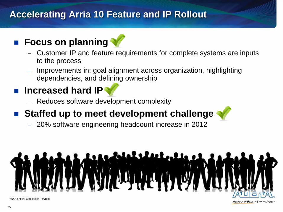
Accelerating Arria 10 Feature and IP Rollout
Focus on planning Customer IP and feature requirements for complete systems are inputs
to the process
Improvements in: goal alignment across organization, highlighting dependencies, and defining ownership
Increased hard IP Reduces software development complexity
Staffed up to meet development challenge 20% software engineering headcount increase in 2012
75

Enpirion Power Solutions

Altera Acquires Enpirion
77

Enpirion Leadership in Integrated Power Conversion
High Efficiency + Low Noise
Up to 97% efficiency with low ripple
Lower system power
Increased System Reliability
Fully simulated, characterized
and validated power system
Fewer components
Ease-of-Use; Faster Time-to-Market
Simple design flow with fewer iterations
Lower development costs
Smallest Footprint
78

Enpirion PowerSoCs Deliver Smallest Footprint
79
Enpirion PowerSoC
Competitor A (Modules)
Competitor B (Discrete Regulators)
Up to 7x Size Reduction
20% lower height than the nearest module competitor

Broad Portfolio of Released Products
Includes 100% Coverage of FPGA Point-of-Load Power Needs
Inductor
Controller
MOSFETS (2x)
High Frequency Filter Caps
DC-DC Power Applications
FPGAs
DDR Memory (VDDQ & VTT)
Processors/CPU
DSP
Product Breadth
1.2V, 3.3V, 5V, &12V switchers
VTT termination
Up to 15A per device
Up to 60A total
80

Altera Validated Solutions Simplify Design Process
Reduce Risk, Effort, Time, Costs
81
Run Early Power Estimator / PowerPlay Power Analyzer
Select Altera Validated PowerSoC
Use Validated FPGA Power Schematics / Gerbers / etc.
Step 1
Step 2
Step 3
First Arria 10 Reference Designs in Q2 2014

Arria 10 Ordering Codes

83
8 →XCVR Count
9 → Transceiver Speed (1,2,3,4)
10 → Package Type (F = 1.0mm, U = .8mm pitch )
11,12 → Package
Arria 10 Family Ordering Code Scheme
1,2 → 10 Series (Arria 10, Stratix 10)
3 → Family (A=Arria, S=Stratix)
4 → Variant (X = GX, T = GT, S=SoC GX)
5,6,7 → 10K LE count
13 → Temp Grade (E=Extended, I=Industrial, M= Mil)
14 → Core Speed (2,3,4)
15 → Power (S = Standard, L = Low, M=Vcc PowerManager)
16 → RoHS (G = RoHS6, P = Leaded*)
17, 18 → ES = Eng. Sample, “Blank” = Production
XCVR Code C E H K N R S U
# of XCVRs 6 12 24 36 48 66 72 96
Package Code U19 – 484 Pins, 19x19 mm F27 – 672 Pins, 27x27 mm F29 – 780 Pins, 29x29 mm F34 – 1152 Pins, 35x35 mm F35 – 1152 Pins, 35x35 mm * F36 – 1152 Pins, 35x35 mm F40 – 1517 Pins, 40x40 mm F45 – 1932 Pins, 45x45 mm
1 2 3 4 5 6 7 8 9 10 11 12 13 14 15 16 17 18 1 0 A X 0 6 7 K 2 F 3 5 I 2 S G E S
Note: F34, F35, F36 are all 35x35 mm packages
F34 – Does not provide vertical migration to F35 or F36
F36 - Provides a 72-bit interface to external memory from
the HPS and provides vertical migration to F35.
F36 is taller in height vs F34 and F35.
* Offered with business justification
Preliminary and subject to change

Why Partner with Altera @20 nm?

Partner With The Technology Leader
85
High-performance and low cost
28 nm FPGAs
Production 28 nm FPGAs
28 Gbps transceivers
14.1 Gbps backplane
transceivers
Hard IP for PCIe Gen1/2/3 x8
DDR3 at 2132 Mbps
DDR3/DDR2/LPDDR2 hard
memory controllers
Variable-Precision DSP blocks
High-precision fractional
synthesis PLLs
Configuration via Protocol (CvP)
40 nm 28 nm
40 nm FPGAs
11.3 Gbps transceivers
Hard IP for PCIe Gen1/2 x8
DDR3 at 1067 Mbps
LC tank-based PLLs for
breakthrough XCVR jitter
performance

Partner With The Technology Leader
40 nm FPGAs
11.3 Gbps transceivers
Hard IP for PCIe Gen1/2 x8
DDR3 at 1067 Mbps
LC tank-based PLLs for
breakthrough XCVR jitter
performance
86
High-performance and low cost
28 nm FPGAs
Production 28 nm FPGAs
28 Gbps transceivers
14.1 Gbps backplane
transceivers
Hard IP for PCIe Gen1/2/3 x8
DDR3 at 2132 Mbps
DDR3/DDR2/LPDDR2 hard
memory controllers
Variable-Precision DSP blocks
High-precision fractional
synthesis PLLs
Configuration via Protocol (CvP)
40 nm 28 nm
Continued Leadership at 20 nm
17.4 Gbps backplane XCVRs
28.05 Gbps XCVRs in a
midrange FPGA
DDR4 at 2600 Mbps
Hard IP for 10GBase- KR/
40GBase-KR4 Forward
Error Correction (FEC)
1.5 GHz hard dual-core
ARM processor
SmartVoltage ID power
reduction
CvP with PCIe Gen3x8
Industry Firsts
From Altera
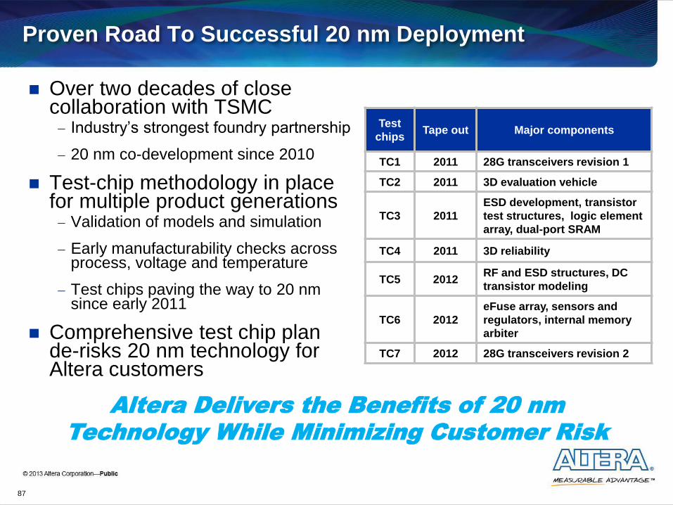
Proven Road To Successful 20 nm Deployment
87
Over two decades of close collaboration with TSMC Industry’s strongest foundry partnership
20 nm co-development since 2010
Test-chip methodology in place for multiple product generations Validation of models and simulation
Early manufacturability checks across process, voltage and temperature
Test chips paving the way to 20 nm since early 2011
Comprehensive test chip plan de-risks 20 nm technology for Altera customers
Test
chips Tape out Major components
TC1 2011 28G transceivers revision 1
TC2 2011 3D evaluation vehicle
TC3 2011
ESD development, transistor
test structures, logic element
array, dual-port SRAM
TC4 2011 3D reliability
TC5 2012 RF and ESD structures, DC
transistor modeling
TC6 2012
eFuse array, sensors and
regulators, internal memory
arbiter
TC7 2012 28G transceivers revision 2
Altera Delivers the Benefits of 20 nm
Technology While Minimizing Customer Risk

Altera 20 nm Transceiver Test Chip Eval Board
88

Altera 20 nm Transceiver Test Chip Lab Setup
89
Lab Setup
20 nm Test Chip Eval Board
20 nm
Test Chip

Industry’s First Transceivers @20 nm Transmit Eye at 32 Gbps
90
First Transceivers @ 20 nm Validate
28G Operation for Arria 10

Altera 20 nm Test Chip, Transceiver Random Jitter
1010 Pattern indicates ultra-low jitter PLL up to 32 Gbps 290 fs Random Jitter
91

Altera 20 nm Test Chip Showing Transmit Eye at 28 Gbps
92
9.05ps Jitter Passes CEI-28G-VSR Specification
With Margin

Arria 10 Summary
Highest performance, lowest power in the midrange Over 60% faster, up to 40% lower power compared to prior
generation mid-range FPGAs
Over 15% faster, up to 60% lower power compared to prior
generation high-end FPGAs
Key features for midrange applications Up to 1.15M logic elements and 53 Mbits embedded block RAM
Up to 96 transceivers up to 28.05G chip-to-chip, up to 17.4G backplane
Footprint-compatible dual-core ARM Cortex A9 SoC options
Over 850 Gbps DDR4 bandwidth
Maximum productivity Quartus II support rolled out in half the time compared to prior generation
OpenCL support for system acceleration
93
Arria 10 FPGAs and SoCs Reinvent the Midrange!

Thank You Thank You

Backup

Portfolio Optimization - The Move from “VI” to “10”
The Need for a Suffix Change
Roman Numerals become challenging beyond “V” Stratix VI or Stratix IV – is too close together
Stratix VII, Stratix VIII, Stratix IX - become very cumbersome/confusing
Introduction of Tri-Gate provides an opportunity Full tailored approach with unprecedented product innovations
Why “10”?
10th Generation FPGA family
Move from Roman to Cardinal numbers (X 10)
Future families will be 20 then 30… Changes the numbering scheme;
Retro to our Flex 10k and Apex 20k days
96