Innovating Power Module Packaging
36
POWER MODULES Innovating Power Module Packaging ISSUE 2 – April/May 2021 www.power-mag.com Also inside this issue Opinion | Market News | Industry News PCIM | Automotive Power | Power Supply Design Energy Harvesting | Website Locator
Transcript of Innovating Power Module Packaging

POWER MODULES Innovating Power Module Packaging
ISSUE 2 – April/May 2021 www.power-mag.com
Also inside this issue Opinion | Market News | Industry News PCIM | Automotive Power | Power Supply Design Energy Harvesting | Website Locator
01_pee_0221.qxp_p01 Cover 20/04/2021 14:45 Page 1

5-7 APRIL 2022 HALLS 9 & 10
NEC BIRMINGHAM
5-7 APRIL 2022HALLS 9 & 10
NEC BIRMINGHAM
BOOK NOW! Contact the team to secure your stand Damien Oxlee +44 (0) 1732 370342 [email protected] Andy Wylie +44 (0) 1732 370341 [email protected]
THE HOME OF AUTOMATION The UK’s leading exhibition for Drives, Automation, Power Transmission and Motion Control Equipment
www.drives-expo.com
IN ASSOCIATION WITH:
CO-LOCATED WITH:
SPONSORS
8 0 % A L R E A D Y S O L D
D&C 2022 A4 Book Now with sponsors.qxp_Layout 1 20/04/2021 05:30 Page 1

CONTENTS
www.power-mag.com Issue 2 2021 Power Electronics Europe
3
Editor Achim Scharf Tel: +49 (0)892865 9794 Fax: +49 (0)892800 132 Email: [email protected]
Production Editor Chris Davis Tel: +44 (0)1732 370340
Financial Manager Clare Jackson Tel: +44 (0)1732 370340 Fax: +44 (0)1732 360034
Reader/Circulation Enquiries Perception Tel: +44 (0) 1825 701520 Email: [email protected]
INTERNATIONAL SALES OFFICES Mainland Europe: Victoria Hufmann Norbert Hufmann Tel: +49 911 9397 643 Fax: +49 911 9397 6459 Email: [email protected]
Eastern US Ian Atkinson Tel: +44 (0)1732 370340 Fax: +44 (0)1732 360034 Email: [email protected] Western US and Canada Ian Atkinson Tel: +44 (0)1732 370340 Fax: +44 (0)1732 360034 Email: [email protected]
Japan: Yoshinori Ikeda, Pacific Business Inc Tel: 81-(0)3-3661-6138 Fax: 81-(0)3-3661-6139 Email: [email protected]
Taiwan Prisco Ind. Service Corp. Tel: 886 2 2322 5266 Fax: 886 2 2322 2205
Publisher & UK Sales Ian Atkinson Tel: +44 (0)1732 370340 Fax: +44 (0)1732 360034 Email: [email protected] www.power-mag.com
Circulation and subscription: Power Electronics Europe is available for the following subscription charges. Power Electronics Europe: annual charge UK/NI £95, overseas $160, EUR 150. Contact: DFA Media, 192 The High Street, Tonbridge, Kent TN9 1BE Great Britain. Tel: +44 (0)1732 370340. Fax: +44 (0)1732 360034. Refunds on cancelled subscriptions will only be provided at the Publisher’s discretion, unless specifically guaranteed within the terms of subscription offer.
Editorial information should be sent to The Editor, Power Electronics Europe, PO Box 340131, 80098 Munich, Germany.
The contents of Power Electronics Europe are subject to reproduction in information storage and retrieval systems. All rights reserved. No part of this publication may be reproduced in any form or by any means, electronic or mechanical including photocopying, recording or any information storage or retrieval system without the express prior written consent of the publisher.
Printed by: Warners.
ISSN 1748-3530
PAGE 6
Market News
PEE looks at the latest Market News and company developments
PAGE 12
Industry News
PAGE 15
PCIM PAGE 25
GaN Raises Electric Vehicle Powertrain Performance In recent years, the number of electric vehicles (EVs) have multiplied on our
global roads. Industry analysts expect that 56 million new EVs will be sold in
2040. The electricity consumption that accompanies this growth will rise to 1,800
TWh, representing 5 % of global power according to Bloomberg NEF’s Electric
Vehicle Outlook. A smart, smaller, lighter-weight powertrain is a key area in
creating changes for the EV industry. Jimmy Liu, Technical Marketing Director,
GaN Systems Inc., Ottawa. Canada
PAGE 28
Novel GaN Design Reduces Volume of AC/DC Converters Substantially In recent years, the number of electric vehicles (EVs) have multiplied on our
Power Integrations recently released a GaN-based IC called MinE-CAP, intended
for use in a new generation of mobile credit card-sized chargers or offline power
supplies. By halving the size of the high-voltage bulk electrolytic capacitors
required in offline power supplies, this IC enables a reduction in adapter size of
up to 40 %. The device also reduces in-rush current making NTC thermistors
unnecessary, increasing system efficiency and reducing heat dissipation.
Andy Smith, Product marketing manager at Power Integrations discusses
this new GaN application in detail.
PAGE 32
Powering Low-Power Sensors for the Internet of Things Low-power sensors for the Internet of Things will be embedded into streets,
offices and factories to collect data for years and share it with the cloud, most
likely wirelessly. The use of batteries as a power source is one of the key areas
developers have to address. It comprises many issues around limited lifetimes,
product sustainability, manufacturing materials, shipment issues and the disposal
of the battery at the end of its life. However, we can look on the bright side as
there is a solution that would allow us to reduce the size of the battery or at least
remove it. Graeme Clark, Principle Engineer, Renesas Electronics
Europe, UK
PAGE 35
Web Locator
Innovating Power Module Packaging A system’s power delivery network or PDN is made up of passive and active components such as cables, connectors, AC-DC and DC-DC converters and regulators. As power levels increase to enable new features and the electrification of mechanical and hydraulic systems, PDN performance is becoming more critical, and in some cases, constraining end system capabilities because of PDN footprint, weight and power losses. Power system design engineers are under increasing pressure to design a PDN that is small, lightweight and highly efficient, as this achievement can define a leadership product capable of delivering major end-system performance and competitive advantages for OEMs. Understanding the importance of these power system design challenges and key PDN performance specifications drives Vicor to constantly innovate to stay on the forefront of power systems technology. To do so requires a major commitment to innovation on many levels. The ChiP packaging approach focuses on the miniaturization of every single component and element that makes up the module. As Vicor makes further improvements in performance, ChiP packaging will exhibit new levels of innovation. For 40 years Vicor has pushed the limits of magnetics and power engineering routinely delivering the next generation of power-dense products for customer’s world-changing innovations. With this momentum and using the five pillars such as Power delivery architectures; Power conversion topologies; Control systems; Components and materials; and Power module packaging as a compass, the journey is nowhere near over. More details on page 22. Cover image supplied by Vicor, USA
FEATURE STORY
p03 Contents.qxp_p03 Contents 20/04/2021 13:28 Page 3

JUMP-START YOUR DESIGN WITH
THE INDUSTRY’S MOSTCOMPREHENSIVE SILICON CARBIDE
POWER SIMULATOR
A Complimentary Service from Wolfspeed
wolfspeed.com/pee-speedfit
/ / / /
28_pee_0121.indd 1 03/03/2021 06:49

OPINION 5
www.power-mag.com Issue 2 2021 Power Electronics Europe
According to Global Market Insights the market for power electronics will cross $30 billion by 2027. The industrial application segment held 25 % of the power electronics market share in 2020 led by increasing acceptance of robotics and automation across manufacturing and process industries. These electrical parts require MOSFETs, IGBTs, and power modules to optimize power and improve the performance capabilities of motor drives for 24/7 operations. The European power electronics market size was over $4 billion in 2020 and is projected to register a 4.5 % growth rate till 2027. The rising deployment of EV charging stations in European economies including Germany, the UK, France, Italy, and Spain will fuel the market demand.
Yole expects that the PHEV and BEV market will grow with around 37 % and 44 % annually until 2026. The converter market for xEV will be worth more than S$29 billion in 2026. The market value for semiconductor power electronic devices for xEVs will reach $5.6 billion in 2026. Over the last couple of years (and especially since Tesla introduced SiC in their Model 3 main inverter), there has been much noise around SiC adoption in EV/HEV. But not all converters or all types of electrification are suitable for this expensive material. BEV is the winner due to the requirements of a long driving range and fast charging time (km driven by charge time). Therefore, the increased cost of the converter is repaid, as the efficiency of the converter will improve, allowing battery savings. The use of SiC in the main inverter has become a common goal for the leading OEMs, with players such as Daimler and Hyundai soon including it in their main inverters. Today, there is already a good portfolio of SiC devices with SiC dies coming from Infineon Technologies, Cree (Wolfspeed), and STMicroelectronics. Many semiconductor players are targeting SiC modules for EV applications, and the SiC module market is expected by Yole to reach 32 % of the total EV/HEV semiconductor market by 2026.
Over the last years, SiC has proven to be a technology of choice for
high voltage and high temperature power electronics devices such as inverters, being able to grant excellent performance in hybrid and full electric applications. The use of SiC MOSFETs enables in fact smaller, lighter and more efficient solutions. These features become even more crucial when it comes to motor sports, where size, weight and efficiency are definitely major design drivers. Thus automotive supplier Marelli has launched its first power module for motorsports electric and hybrid traction applications completely developed in the company’s Corbetta facility, fully based on SiC technology and using a new direct cooling solution for more efficient, compact and lighter inverters.
Also GaN transistors are being implemented more and more in EV powertrain systems which highlight confidence in its reliable out performance and benefits on system cost, density, efficiency, and weight. Examples of OBC, DC/DC converter, and traction inverter products that demonstrate the GaN’s high performance advantages are shown in our feature “GaN Raises Electric Vehicle Powertrain Performance”.
And the total market value of power electronic devices for EV DC chargers will grow to around $350 million by 2026 at an annual growth rate of roughly 40 %. The total market value of power electronic devices for DC chargers will grow with a CAGR 2020-2026 of 21.5 %.
But the COVID-19 pandemic has resulted in severe disruption in supply chain for semiconductor raw materials and components across the globe. The market participants are highly dependent on China for procuring raw materials and components for manufacturing power electronics devices. To fix the supply chain issues, companies are establishing new production facilities in their countries and other regions, adding new opportunities to regional raw material suppliers.
Also the COVID-19 pandemic has affected the power electronic events such as PCIM and APEC.
In February the decision was made to postpone the PCIM Europe to late summer following talks with exhibitors and partners. In light of the ongoing pandemic and challenging situation, numerous industry players have been hesitant to commit to an on-site event. For this reason, Mesago has decided to hold PCIM again as a digital event only. Over five days, power electronic suppliers and users can receive information on key developments and connect in a variety of ways. In addition to extensive exhibitor profiles, the conference program will consist of presentations as a mix of live and video-on-demand presentations, followed by discussions with the speakers. A major part of the conference is dedicated to key innovations in order to significantly increase the power density of components and systems. Moreover, focus is placed on new materials to achieve a technology breakthrough towards elevated operating temperature along with an extended lifetime of devices and smart digital controlled power conversion concepts for automotive and industry applications (see our PCIM preview).
Also the organizers of APEC 2021 announced early April that the event, previously planned as in-person event in the Phoenix/AZ Convention Center from June 9 – 12, will be presented on the virtual platform Social27 from June 14 - 17 with on demand access starting the week of June 9. Since home life has changed over the past several months the daily schedule has been modified slightly to make the conference as accessible as possible during the workweek. All sessions will be recorded so the content can be viewed on own schedule. Attendees will be granted access to the virtual event platform and all on-demand sessions during the week of June 9, 2021. On-demand recordings will include: technical session lectures and dialogues (poster sessions), industry sessions, and professional education seminars. This will also provide attendees with time to build their attendee profiles, and get acquainted with the site.
We will provide all relevant information in a timely manner. Enjoy reading this issue!
Achim Scharf PEE Editor
Despite Covid-19 Automotive Accelerate WBG Applications
05_pee_0221.qxp_p05 Opinion 20/04/2021 11:40 Page 5

6 MARKET NEWS
Issue 2 2021 Power Electronics Europe www.power-mag.com
According to the latest report “Power Electronics Market” by Global Market Insights Inc., the market valuation of power electronics will cross $30 billion by 2027.
The market growth is attributed to the increasing adoption of power electronics modules in consumer electronics and smart home appliances. These modules are extensively incorporated into HVAC control systems, smart energy meters, robotic vacuums, air conditioners, smart TVs, and other smart appliances to prevent from electrocutions and increase the power efficiency of the devices. The power modules also help device manufacturers to achieve optimized system costs and provide low-noise features in smart home appliances. Adding to this, the rising integration of AI and IoT technologies into smart home technology products will further boost the market expansion during the forecast period.
The industrial application segment held 25 % of the power electronics market share in 2020 led by increasing acceptance of robotics and automation across manufacturing and process industries. The industrial robots are integrated with various parts such as motor drives, robot arms, servo motors, and controllers. These electrical parts require MOSFETs, IGBTs, and power modules to optimize power and improve the performance capabilities of motor drives for 24/7 operations. The proliferation of industrial robots is
anticipated to foster industry growth during the forecast timeframe. The European power electronics market size was over $4 billion in 2020 and is projected to register a 4.5 % growth rate till 2027. The rising deployment of EV charging stations in European economies including Germany, the UK, France, Italy, and Spain will fuel the market demand. According to the Department for Transport, the Government of the UK, in January 2021, there were 20,775 public electric vehicle charging devices in the UK, of which, 3,880 were rapid charging devices. These battery-power establishments and rapid EV charging stations have high adoption of power electronics. The proliferation of EVs and EV charging stations in the UK are poised to impel industry value.
But the COVID-19 pandemic has resulted in severe disruption in supply chain for semiconductor raw materials and components across the globe. The market participants are highly dependent on China for procuring raw materials and components for manufacturing power electronics devices. To fix the supply chain issues, companies are establishing new production facilities in their countries and other regions, adding new opportunities to regional raw material suppliers during the forecast timeline.
https://www.gminsights.com/request-sample/detail/1355
Power Electronics Market Revenue to Cross $30 Billion by 2027
Market researcher Yole expects that the PHEV and BEV market will grow with around 37 % and 44 % annually until 2026. The converter market for xEV will be worth more than S$29 billion in 2026 with a CAGR 2020-2026 of 28 %. The market value for semiconductor power electronic devices for xEVs will reach $5.6 billion in 2026 with a CAGR2020-2026 of 26 %.
“There are basically three converter types in an electric car: the main inverter, DC/DC and OBC,” asserts Ana Villamor, Technology & Market Analyst, Power Electronics at Yole. “The main inverter is the largest market among the different converters due to the higher power levels, leading also to the highest content of power semiconductors.” Thus, the main inverter market is expected to reach $19.5 billion by 2026, representing 67 % of the total EV/HEV converter market, with a CAGR of 26.9%. Regarding the power semiconductor market, its value is expected to triple from 2020 to 2026, driven by a major technology battle between IGBT and SiC modules. Indeed, SiC modules are presently still about x3 the cost of a 650 V IGBT module, but this difference will shrink when larger volumes are produced, with the transition to 8-inch wafers, and with the penetration of 1,200 V devices for higher battery voltages.
A analyzed by Yole’s team in the new Power Electronics for E-Mobility 2021 report, the EV/HEV supply chain continues to be impacted by the increased demand and technology trends. Although the leading semiconductor manufacturers for EV/HEV remain the same as for other power applications. It includes Infineon Technologies, STMicroelectronics, Hitachi, Mitsubishi Electric, ON Semiconductor. Other companies, Tier 1s, OEMs, power semiconductor manufacturers, and pure module newcomers, are now offering power modules for EV/HEV. A similar situation occurs with the battery design and manufacturing, where OEMs such as Tesla and GM are further trying to control their supply chains. According to Milan Rosina, Principal Analyst, Power Electronics & Batteries at Yole: “Competition at OEM level has also opened two main fronts: on the one hand, there are the traditional OEMs with established markets and known brands that are transforming their business towards electric vehicles. On the other hand, pure EV OEMs are popping up in the different regions of the world (such as NIO, Rivian, Rimac, Xpeng, and Hozon), some of which are rapidly increasing their volumes year after year (lead by Tesla)”. The new car models being launched often offer better
performance/cost ratio, and this has led to a continuous reshaping of the top 10 vehicle sales.
SiC is now walking the EV/HEV red carpet. Over the last couple of years (and especially since Tesla introduced SiC in their Model 3 main inverter), there has been much noise around SiC adoption in EV/HEV. But not all converters or all types of electrification are suitable for this expensive material. Without a doubt, BEV is the winner due to the requirements of a long driving range and fast charging time (km driven by charge time). Therefore, the increased cost of the converter is repaid, as the efficiency of the converter will improve, allowing battery savings. It is no surprise then that the use of SiC in the main inverter has become a common goal for the leading OEMs, with players such as Daimler and Hyundai soon including it in their main inverters.
Today, there is already a good portfolio of SiC devices with SiC dies coming from Infineon Technologies, Cree (Wolfspeed), and STMicroelectronics. Many semiconductor players are targeting SiC modules for EV applications, and the SiC module market is expected by Yole to reach 32 % of the total EV/HEV semiconductor market by 2026.
www.yole.fr
E-Mobility Adopts Silicon Carbide
Market news.qxp_Layout 1 20/04/2021 12:31 Page 6

MARKET NEWS 7
www.power-mag.com Issue 2 2021 Power Electronics Europe
The safe routeto EV charging
CDSR Series
When it comes to EV charging, you don’t compromise on safety – and neither do we.
Using the latest flux gate open loop technology, the LEM CDSR leakage current sensor ensures a high degree of safety for EV users by measuring AC and DC leakage current below 1mA at frequencies up to 2kHz.
The LEM CDSR is also highly compact, keeping space needs to a minimum while remaining fully compliant with relevant standards. In addition, it provides highly flexible connectivity, offering both cable IC-CPD (mode 2) and AC wallbox (mode 3).
• Single and three phase configuration
• 32 Arms nominal current per phase
• 0.5 mA accuracy at 6mA
• Test winding and default output signal
• Analog and digital communication (SPI)
• Complies with application standards
IEC 61851, 62955, 62752, UL 2231
www.lem.com
Automotive supplier Marelli has launched its first power module for motorsports electric and hybrid traction applications completely developed in the company’s Corbetta facility, fully based on Silicon Carbide technology and using a new direct cooling solution for more efficient, compact and lighter inverters.
Over the last years, Silicon Carbide has proven to be a technology of choice for high voltage and high temperature power electronics devices such as inverters, being able to grant excellent performance in hybrid and full electric applications. The use of SiC MOSFETs enables in fact smaller, lighter and more efficient solutions. These features become even more crucial when it comes to motorsports, where size, weight and efficiency are definitely major design drivers.
The new module, called EDI (Enhanced Direct-cooling Inverter), was developed by Marelli Motorsport with the Fraunhofer Institute for Reliability and Microintegration IZM in Germany and features an innovative structural design that drastically reduces the thermal resistance between the SiC components themselves and the liquid coolant, thanks to a new baseplate-less solution. The result is an extremely compact power stage, which can exploit the efficiency advantage of Silicon Carbide, allowing vehicle designers more flexibility in packaging, cooling system design and minimized energy storage.
In comparison to a Silicon-based design of the same rating, the new technology enables conversion efficiencies of up to 99.5 %, 50 % reduction in weight and size and 50 % higher heat dissipation into cooling system. Produced in the clean room of Marelli Corbetta facility (Italy), the EDI power
SiC for Traction in Motorsport
Motorsport SiC module produced in the clean room of Marelli Corbetta facility
module has already successfully undergone a series of reliability qualification tests for motorsports mission profiles, to assess the robustness of the design when subjected to thermal cycles, switching tests, and pressure cycles.
This new significant achievement is a further step forward within Marelli ongoing commitment in the field of electric powertrain, which is focused on developments both for motorsport and road vehicles applications and can rely on the company’s combined expertise in electric drives and thermal energy management systems. “Being at the forefront of motorsports technologies requires a continuous drive for innovation, also based on a constant research
Market news.qxp_Layout 1 20/04/2021 12:31 Page 7

Issue 2 2021 Power Electronics Europe www.power-mag.com
for the most efficient materials and solutions” said Riccardo De Filippi, Senior Vice President and CEO of Marelli Motorsport. “Our mission is to promote technological advancements that can first of all be decisive on racetracks, and at the same time enable next-generation technologies also for the road cars of tomorrow. Specifically, in the electric powertrain field, we can build on our strong experience as pioneers of cutting-edge solutions for F1 and Formula E, as well as early adopters of SiC technologies.”
In March 2020, Marelli additionally announced a strategic partnership with Transphorm to collaborate on new GaN-based automotive/EV power conversion solutions including on-board chargers (OBCs), DC/DC converters and powertrain inverters for electric and hybrid vehicles.
Dr. Joachim Fetzer, CEO, Electric Powertrain Marelli, commented,
“Transphorm’s demonstration of achieving 10 kilowatts of power from a discrete packaged GaN device in a bridge configuration is further validation of the exciting promise of GaN for electric vehicle converters and inverters. As part of our previously announced partnership, we will continue to evaluate Transphorm’s industry leading GaN devices and work together in support of a multi-year EV systems product roadmap.”
MARELLI is one of the leading global independent suppliers to the automotive sector. With around 60,000 employees worldwide, its footprint includes 170 facilities and R&D centers across Asia, the Americas, Europe, and Africa, generating revenues of 13.6 billion Euro in 2019.
www.marelli.com
DC EV Charging - A Decisive OutlookThe total market value of power electronic devices for DC chargers will grow to around $350 million by 2026 at an annual growth rate of roughly 40 %, according to market researcher Yole. The total market value of power electronic devices for DC chargers will grow with a CAGR 2020-2026 of 21.5 %.
“While low-power DC chargers, up to 20-30 kW, are commonly based on a monolithic design approach, the modular design is dominant in high-power chargers.”asserts Milan Rosina, Principal Analyst, Power Electronics and Batteries at Yole. “In the modular approach, a charger is built of several charger modules connected in parallel. The modular approach has advantages of high design flexibility, scalability, and availability.”
As analyzed by Yole’s team in the new DC Charging for Plug-In Electric Vehicles 2021 report, discrete devices are suitable for both low-power monolithic chargers and high-power chargers based on low-power charger modules, and thus discrete devices dominate the DC EV market. However, with increasing charger power, the number of related low-power charger modules is increasing beyond optimal levels. For example, for a 350 kW charger about 12 30 kW charger modules will be needed. Charger module manufacturers are looking to improve their products’ power density, efficiency, and to increase their nominal power to 50 kW and beyond to make them more suitable for high-power chargers. “DC charger technology rapidly evolves, and many technology trends were identified and analyzed in this report. Two opposite trends exist regarding charger power. One is a power increase up to 350 kW and beyond in the future to accelerate charging and enable charging in heavy-mobility applications. The other is a power decrease from a historical base level of 50 kW as an alternative to AC charging solutions”, Rosina comments.
Charger voltage follows the trends in EV battery packs. As battery voltage increases from 400 V to 800 V levels, driven by Porsche, Hyundai and other car makers, the charger voltage increases from 500 V to 1,000 V. This results in the chargers using power components rated at 1,200 V. Other trends include increasing use of SiC MOSFET devices, growing market share of power modules, bidirectional chargers for V2G and V2H applications, and battery energy storage to reduce peak loads on the electricity grid. Regulations and technologies for EVs, EV
batteries and chargers evolve rapidly. This brings new opportunities or threats to the charging infrastructure companies such as ABB, Tritium and Tesla, but also to the companies involved in semiconductor and packaging materials, device packaging, industrial systems, EV/HEV and battery manufacturers, and utility companies. Technology or business model differentiation is difficult to identify currently.
“We therefore expect the reshaping of the supply chain and business models to continue in the coming years. Partnerships are crucial to ensure the compatibility between vehicle and charger, and can provide some level of product differentiation”, said Abdoulaye Ly, Technology & Market Analyst. “One example is the network of 350 kW chargers operated by IONITY, backed by several leading car makers, including Volkswagen, BMW and Hyundai. Both car makers and utility companies have identified the opportunities in providing services to a large and rapidly growing portfolio of PHEV and BEV customers.”
An increase of merger and acquisition activities is expected with charging infrastructure providers as main targets. High-power chargers, fast-charging batteries and efficient vehicle powertrains represent a threat to the companies involved in hydrogen infrastructure and fuel-cell vehicles such as Toyota and Honda, and might also close the opportunity
window for companies involved in battery swap solutions like NIO and Aulton. “Strict CO2 targets will push EV/HEV share to 38 % of all passenger vehicles in 2026, representing a $5.6 billion market opportunity for various semiconductor technologies and power devices,” Ly concluded.
Yole’s analysts invites our readers to join them at the PCIM Europe 2021 digital days.
On May 4 Abdoulaye Ly, Technology & Market Analyst specialized in Electronic Power Systems, will present the “EV DC Chargers, a New Opportunity for Power Electronic Players”. Ana Villamor, PhD, Technology & Market Analyst, Power Electronics & Milan Rosina, PhD, Principal Analyst, Power Electronics and Batteries, will present “Battery, SiC, 800V…What else is needed by an Electric Vehicle Manufacturer to Differentiate from its Competitors?”
On May 5 Shalu Agarwal, Technology & Market Analyst, Power Electronics & Materials will present “Power Module Packaging: Good enough Aspect is a New Target” at 2:00 pm during the Industry Forum. Registration under http://www.i-micronews.com/event/pcim-europe-2021/?utm_source=PR&utm_medium=email&utm_campaign=PR_DC_CHARGING_FOR_PLUG_IN_ELECTRIC_VEHICLES_YOLE_April2021
www.yole.fr
8 MARKET NEWS
Market news.qxp_Layout 1 20/04/2021 12:31 Page 8

9
www.power-mag.com
MARKET NEWS
GeneSiC Released 3rd Generation SiC MOSFETs
GeneSiC Semiconductor’s next-generation 1200V G3R™SiC MOSFETs deliver on-resistance levels ranging from 20 mΩ to 350 mΩ. System benefits include higher efficiency, faster switching frequency, increased power density, reduced ringing (EMI) and compact system size.
These SiC MOSFETs, offered in optimized low-inductance discrete packages (SMD and through hole), are highly optimized for power system designs requiring elevated efficiency levels and ultra-fast switching speeds. “After years of development work towards achieving the lowest on-state resistance and enhanced short circuit performance, we released the industry’s best performing 1200V SiC MOSFETs with over 15+ discrete and bare chip products. If the next-generation power electronics systems are to meet the challenging efficiency, power density and quality goals in applications like automotive, industrial, renewable energy, transportation, IT and telecom, then they require significantly improved device performance and reliability,”said Dr. Ranbir Singh, President at GeneSiC Semiconductor.
G3R SiC MOSFETs are designed to be driven at +15V / -5V gate drive. This offers broadest compatibility with existing commercial IGBT and SiC MOSFET gate drivers.
www.genesicsemi.com/sic-mosfet/
Volkswagen’s High-Manganese Cathode StrategyWhilst relatively light on technical content, an interesting point during Volkswagen’s recent Power Day referred to their long-term strategy of employing high-manganese cathodes for their ‘volume segment’ - a prominent role for a chemistry not currently in widespread use. Improvements to energy density are unlikely using high-manganese cathodes, with motivation for developing these materials instead stemming from a desire to reduce cost and eliminate cobalt consumption. But what does ‘high-manganese’ refer to, and how do they compare to other cathode materials? A commentary by IDTechEx.
‘High-manganese’ cathodes could refer to several different materials, and so it is unclear as to the specific material Volkswagen were referring to. The options for high-manganese cathodes include LMO (lithium-manganese oxide), LNMO (lithium-nickel-manganese oxide), Li-Mn-rich (also abbreviated as LMR-NMC), and LMP (lithium manganese phosphate) or LMFP (lithium-manganese-iron phosphate). A comparison between NMC 811 and three high-manganese cathodes (LMFP, Li-Mn-rich, LNMO) shows that trade-offs in performance are always involved. Delving deeper into each option can help provide some insight
We make cars go
We help power the EV and e-mobilityplatforms of today & the future
Insulated Litz for High-Frequency Applications
Triple Insulated Winding Wires for PowerElectronics
UL & VDE certifications for applications up to1,500 Vpk and thermal classes of 155°C and 180°C
Specialty Litz conductors for applications up to260°C
Rubadue.com +1 970.351.6100
E P . M E R S E N . C O M
N E X T- GE N BAT TE RY CE LL S CONNECTION AND MONITORING
FOR E- MOBILIT Y•Re d uce footp r in t
o f th e bat te r y asse m b l ies
•M o du la r and f l ex ib le des ign fo r eve r y p la t fo rms
•D es ign e d fo r l a rge sc a le man ufac tu r ing
•Adaptat ive fo rm -fac to r
•S ing le - l aye r l a se r-we lde d in te r l eave d b usba r
D es ign e d fo r l a rge sc a le man ufac tu r ing
•Adaptat ive fo rm -fac to r
•S ing le - l aye r l a se r-we lde d
D es ign e d fo r l a rge sc a le man ufac tu r ingD es ign e d fo r l a rge sc a le man ufac tu r ing
Adaptat ive fo rm -fac to rAdaptat ive fo rm -fac to r
S ing le - l aye r l a se r-we lde d in te r l eave d b usba r
S ing le - l aye r l a se r-we lde d
Adaptat ive fo rm -fac to rAdaptat ive fo rm -fac to r
D es ign e d fo r l a rge sc a le man ufac tu r ingD es ign e d fo r l a rge sc a le man ufac tu r ing
S ing le - l aye r l a se r-we lde d S ing le - l aye r l a se r-we lde d
D es ign e d fo r l a rge sc a le man ufac tu r ingD es ign e d fo r l a rge sc a le man ufac tu r ing
Adaptat ive fo rm -fac to rAdaptat ive fo rm -fac to r
S ing le - l aye r l a se r-we lde d in te r l eave d b usba r
S ing le - l aye r l a se r-we lde d
D es ign e d fo r l a rge sc a le man ufac tu r ing
Adaptat ive fo rm -fac to r
S ing le - l aye r l a se r-we lde d
D es ign e d fo r l a rge sc a le man ufac tu r ing
Adaptat ive fo rm -fac to r
S ing le - l aye r l a se r-we lde d in te r l eave d b usba rin te r l eave d b usba rin te r l eave d b usba rin te r l eave d b usba rin te r l eave d b usba rin te r l eave d b usba rin te r l eave d b usba r
D es ign e d fo r l a rge sc a le man ufac tu r ingD es ign e d fo r l a rge sc a le man ufac tu r ingD es ign e d fo r l a rge sc a le man ufac tu r ing
••Adaptat ive fo rm -fac to rAdaptat ive fo rm -fac to rAdaptat ive fo rm -fac to rAdaptat ive fo rm -fac to rAdaptat ive fo rm -fac to rAdaptat ive fo rm -fac to rAdaptat ive fo rm -fac to rAdaptat ive fo rm -fac to rAdaptat ive fo rm -fac to rAdaptat ive fo rm -fac to rAdaptat ive fo rm -fac to r
•••S ing le - l aye r l a se r-we lde d S ing le - l aye r l a se r-we lde d S ing le - l aye r l a se r-we lde d S ing le - l aye r l a se r-we lde d S ing le - l aye r l a se r-we lde d S ing le - l aye r l a se r-we lde d S ing le - l aye r l a se r-we lde d S ing le - l aye r l a se r-we lde d S ing le - l aye r l a se r-we lde d S ing le - l aye r l a se r-we lde d in te r l eave d b usba rin te r l eave d b usba rin te r l eave d b usba rin te r l eave d b usba rin te r l eave d b usba rin te r l eave d b usba rin te r l eave d b usba rin te r l eave d b usba rin te r l eave d b usba rin te r l eave d b usba r
Market news.qxp_Layout 1 20/04/2021 13:32 Page 9

10 MARKET NEWS
Issue 2 2021 Power Electronics Europe www.power-mag.com
into what specific material might be being developed for use. LMO (LiMn2O4) - firstly, commercially available high-manganese cathodes
already exist in the form of the lithium-manganese oxide spinel, which was used for the 1st generation Nissan Leaf cars. However, it suffers from accelerated degradation at elevated temperatures, which leads to poor cycle life, hence the replacement of LMO with NMC in subsequent Nissan Leaf generations. With a theoretical capacity of only 148 mAh/g and an average discharge voltage of approximately 4.0-4.1 V, this cathode would lead to lower energy densities compared to cells using current state-of-the-art NMC or NCA layered oxides.
LMP (LiMnPO4) and LMFP (LiMnxFe1-x¬PO4) - LMP shares the same olivine crystal structure as LFP but operates at a more positive voltage, increasing energy density. Cycle life tends to be low, due to the high manganese content, while the material has poor electronic and ionic conductivity, meaning that reasonable capacities are generally only measured at low charge/discharge rates. The addition of Fe to form LMFP can improve conductivity and cycle life but lowers the average voltage. LMFP may bridge the gap between LFP and NMC/NCA but the reversible capacities of LMP and LMFP are too low to reach the cell-level energy densities of cells using NMC/NCA.
Li-Mn-rich (xLi2MnO3·(1 - x)LiMO3 where M = Ni, Mn, Co) - the lithium-manganese rich, layered-oxide cathode is one of only a few options, alongside conversion type cathodes, that offer a capacity improvement over current state-of-the-art NMC and NCA materials. However, stability and cycle life are poor and require considerable improvement before commercialization can be expected. BASF’s high manganese cathode, NCM 217, may refer to a Li-Mn-rich type material.
This leaves LNMO as the most likely cathode VW were referring to. The high-voltage LNMO spinel (LiNi0.5Mn1.5O4) operates at a voltage of approximately 4.7 V vs. Li/Li+ and also holds potential as a high-power cathode due to its three-dimensional structure (improving Li diffusion pathways). However, its theoretical specific capacity is only 147 mAh/g, meaning it will not offer any advantage to specific energy or energy density over high-Ni NMC or NCA cathodes.
Furthermore, key issues with LNMO revolve around its low cycle life and poor
stability, especially at elevated temperatures, whilst its high voltage also necessitates developments to electrolytes. As outlined by Volkswagen themselves, the use of high-manganese cathodes represents a long-term strategy.
Nevertheless, there is some commercial development of LNMO from the likes of Haldor Topsoe, NEI Corporation, and Targray. The potential for cost reduction that the material holds, without significantly reducing energy density, added to the possibility of eliminating cobalt consumption, suggests there is a future for this chemistry. The graph below shows how both nickel and cobalt intensity can be reduced by high manganese cathodes such as LNMO, offering a path to lower Li-ion battery costs.
Given the trade-off between cost and different performance metrics from different Li-ion cathodes, a range of cathode materials will have to be employed by the Li-ion industry. Further detail and analysis of Li-ion technology trends, and their impact on battery material demand forecasts, can be explored in IDTechEx’s reports “Li-ion Batteries 2020-2030” and “Materials for Electric Vehicle Battery Cells and Packs 2021-2031”.
www.IDTechEx.com/Research/ES
The US ended 2020 with record wind and solar additions, beating previous highs in all sectors, according to BloombergNEF’s (BNEF) 1H 2021 Renewable Energy Market Outlook. The next ten years will see the US wind and solar fleet almost triple.
The US is about to see five years of record large-scale solar capacity additions, adding over 20 GW each year. Both large- and small-scale solar will grow during the years of tax credit extensions.
Over the coming decade customer-sited solar capacity maintains its pace, adding on average over 8 GW a year. Over a third of all new systems are built in California. Storage becomes more relevant for project economics as net metering is phased out.
Onshore wind is set for another big year of build after a record beating 2020. Installs fall from 2022 as tax credits continue to be reduced. After tax credits are removed in 2026, build dips as projects rely only on the merchant market. Offshore
wind looks set to be the big winner of the Biden presidency. The administration seems committed to resolving longstanding permitting bottlenecks and the sector will enjoy a new dedicated tax credit. However, this will still not be enough to hit the Biden administration’s stated goal of decarbonizing the power sector by 2035. “Even without details from the American Jobs Plan, wind and solar capacity additions will steadily grow over the decade, adding 287GW of solar and 115GW of wind. Solar in particular will see record growth in the next four years, adding over 25 GW each year across all sectors. However, more renewables will likely be needed to come close to the government’s target of zero emissions by 2035,” commented Tara Narayanan, BNEF lead US solar analyst.
The American Jobs Plan also mentioned, in passing, a “Clean Energy Standard”, which, if anything like the Renewable Portfolio
Standards implemented by certain states, could close that gap. However, such a standard is likely to prove contentious politically and would face a difficult passage through Congress if proposed, and potentially legal challenges from states and utilities. Tax credits certainly help the renewables sector grow, but a Clean Energy Standard is the hill on which the battle to fully decarbonize the US power sector could be won or lost.”If the US is to achieve a carbon free grid by 2035 then it would need to at the very least add around 70 GW of wind and solar a year from 2025 onwards - whereas our forecast sees an average of 43 GW per year after 2025. So while we see significant progress for the sector, there is still a significant gap between our outlook and the administration’s ambitions,” adds Tom Rowlands Rees, BNEF head of North America research.
https://about.bnef.com/
US Record Wind and Solar Additions
Market news.qxp_Layout 1 20/04/2021 12:31 Page 10

MARKET NEWS 11
www.power-mag.com Issue 2 2021 Power Electronics Europe
SEMIKRON and Silicon Mobility BEV Inverter CollaborationPSEMIKRON and Silicon Mobility, a solution provider of digital control for electrified powertrain, announced the availability of a 24 V to 96 V inverter platform for battery powered vehicles and industrial off-road vehicles.
The inverter platform delivers from 10 kW to 50 kW and combines the SEMIKRON SKAI® 3 LV inverter and Silicon Mobility OLEA® inverter and electric motor control solution.
SEMIKRON provides the power and assembly with an advanced integrated MOSFET module with connected DC-link, gate-driver, protection functions, and sensors. It comes with a complete 3-phase motor-drive and a ready-made power section to offer an ultra-compact MOSFET inverter. The converter connects easily to a custom control board for quick and easy designing, while leaving the control to the customer. The OLEA T222 Starter Kit includes a reference control board integrating T222 FPCU, a powerful control chip, and APP INVERTER, a control software application adapted for the SKAI 3 LV inverter power module, fully configurable to support a wide variety of 3-phase PMSM and WRSM electric motor and position sensors. The
application provides efficient and safe torque and speed management using Field Oriented Control (FoC) and variable
Space Vector Pulse Width Modulation (SVPWM) algorithms from 2 kHz up to 100 kHz. Calibration and validation are enabled thanks to its native ASAM standard support. The starter kit also includes vehicle dependent software demo code, post-build measurement, configuration, calibration, and firmware update GUI software. The platform is accessible as a White Box where users can customize upon request the power module packaging/casing from SEMIKRON and access the OLEA APP INVERTER object code through a dedicated license. “With this platform, we give low-voltage vehicle manufacturers access to technologies and solutions far above today’s state of the art implementations, providing them the extra edge for their designs,” commented Karl-Heinz Gaubatz, CEO/CTO SEMIKRON International. “By choosing this platform, vehicle manufacturers can accelerate the electrification of their vehicles and offer themselves the possibility of future differentiation,” added Rainer Kallenbach, CEO Silicon Mobility.
www.semikron.com, www.silicon-
mobility.com
To receive your own copy of
Power Electronics Europe
subscribe today at:
www.power-mag.com
“With our 24 V to 96 V inverter platform we give low-voltage vehicle manufacturers access to technologies and solutions far above today’s state-of-the-art implementations,” said SEMIKRON’s CEO Karl-Heinz
Market news.qxp_Layout 1 20/04/2021 12:31 Page 11

12 INDUSTRY NEWS
Issue 2 2021 Power Electronics Europe www.power-mag.com
The 70 mΩ NV6128 represents a 66 % increase in current capability, in a small, 6 x 8 mm PQFN package with a proprietary, integrated cooling pad for high-efficiency, high-density power systems. The NV6128 is rated at 650 V for nominal operation plus a 800 V peak capability for robust operation during transient events. As a power IC, the GaN gate is protected and the device rated at an electrostatic discharge (ESD) specification of 2 kV. “GaNFast power ICs have been broadly adopted by tier-1 names like Lenovo, Dell, OPPO and Xiaomi for fast-charging mobile adapters up to 200 W, with over 13,000,000 shipped and zero failures,” noted Gene Sheridan, Navitas CEO and co-founder.
“With the higher-power NV6128, we extended the effective power range to 500 W for the consumer market and look beyond that to multi-kW data center, eMobility and new energy applications.”
The NV6128 is in high-volume, mass production by TSMC and available from Navitas’ distribution partners at $7.85 at 1k units.
Operating modes When the VCC supply is first applied to the GaNFast power IC, care should be taken such that the VDD and DZ pins are up at their correct voltage levels before the PWM input signal starts. The VDD pin ramp up time is determined by the internal regulator current at this pin and the external CVDD capacitor. CVDD time constant should be calculated such that there is sufficient time to charge up the CVDD capacitor to ~6 V. In some scenarios, where fast startup is required, an optional diode in parallel with the RDD can be used to ensure the CVDD capacitor is fully charged before the first PWM pulse is applied. Also, since the DZ pin voltage sets the VDD voltage level, the VDD pin will ramp up together with the DZ pin (Figure 1).
During Normal Operating Mode, all of the internal circuit blocks are active. VCC is operating within the recommended range of 10 V to 24 V, the VDD pin is at the voltage set by the Zener diode at the DZ pin (6.2 V), and the internal gate drive and power FET are both enabled.
The Zener voltage is a critical parameter that sets the internal reference for gate drive voltage and other circuitry. The Zener diode needs to be selected such that the voltage on the DZ pin is within recommended operating conditions (5.8 V to 6.6 V) across operating temperature (-40°C to 125°C) and bias current (10 �A to 1 mA). To ensure effective operation, the current vs. voltage characteristics of the Zener diode should be measured down to 10 ?A to ensure flat characteristics across the current operating range (10 �A to 1 mA). If the Zener selected by user does not ensure that the voltage on the DZ pin is always within the recommended operating range, the functionality and reliability of the GaNFast power IC can be impacted.
The external PWM signal at the PWM pin determines the frequency and duty-cycle of the internal gate of the power FET. As the PWM voltage toggles
GaNFast IC Delivers 66 Percent More PowerNV6128, a new high-power 650 V/800 V-rated GaNFast power IC to address the high-power mobile and consumer power electronics market. Gallium nitride (GaN) is a next-generation semiconductor technology that runs up to 20x faster than Silicon and enables up to 3x more power or 3x faster charging in half the size & weight. GaNFast power ICs integrate GaN power and drive plus protection.
Figure 1: Start-up circuit (upper) and LLC half-bridge start-up timing diagram (lower image) Figure 2: Turn-on dV/dt slew rate control
Industry.qxp_Layout 1 20/04/2021 11:47 Page 12
INDUSTRY NEWS 13
www.power-mag.com Issue 2 2021 Power Electronics Europe
above and below the rising and falling input thresholds (4 V and 1 V), the internal gate of the power FET toggles on and off between VDD and 0 V. The drain of the power FET then toggles between the source voltage (typically power ground) and a higher voltage level (650 V max), depending on the external power conversion circuit topology.
Programmable turn-on dV/dt control During first start-up pulses or during hard-switching conditions, it is desirable to limit the slew rate (dV/dt) of the drain of the power FET during turn-on. This is
as much as possible. To further reduce high-frequency noise, this GaN Power IC includes two Source Kelvin (SK) pins. The SK pins are on-chip kelvin contacts to the Source and are separate from the high current Source connections.The GND connections for components CVDD and DZ should be connected to SK pin, and the GND connection for CVCC should be connected to CP pin 30. SK pin 29 should be left unconnected (N/C). When
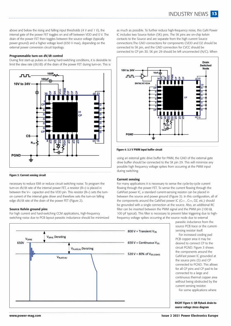
Figure 3: Current sensing circuit
Figure 4: 3.3 V PWM input buffer circuit
necessary to reduce EMI or reduce circuit switching noise. To program the turn-on dV/dt rate of the internal power FET, a resistor (RDD) is placed in between the VDD capacitor and the VDD pin. This resistor (RDD) sets the turn-on current of the internal gate driver and therefore sets the turn-on falling edge dV/dt rate of the drain of the power FET (Figure 2).
Source Kelvin ground pins For high current and hard-switching CCM applications, high-frequency switching noise due to PCB layout parasitic inductance should be minimized
using an external gate drive buffer for PWM, the GND of the external gate drive buffer should be connected to the SK pin 29. This will minimize any possible high frequency voltage spikes from occurring at the PWM input during switching.
Current sensing For many applications it is necessary to sense the cycle-by-cycle current flowing through the power FET. To sense the current flowing through the GaNFast power IC, a standard current-sensing resistor can be placed in between the source and power ground (Figure 3). In this configuration, all of the components around the GaNFast power IC (CVCC , CVDD, DZ, etc.) should be grounded with a single connection at the source. Also, an additional RC filter can be inserted between the PWM signal and the PWM pin (100 Ω, 100 pF typical). This filter is necessary to prevent false triggering due to high-frequency voltage spikes occurring at the source node due to external
parasitic inductance from the source PCB trace or the current-sensing resistor itself.
For increased cooling pad PCB copper area it may be desired to connect CP to the circuit PGND. Figure 3 shows the components around the GaNFast power IC grounded at the source pins (S) and CP connected to PGND. This allows for all CP pins and CP pad to be connected to a large and continuous thermal copper area without being obstructed by the current sensing resistor.
For some applications where
RIGHT Figure 5: QR flyback drain-to-source voltage stress diagram
Industry.qxp_Layout 1 20/04/2021 11:47 Page 13

14 INDUSTRY NEWS
a 3.3 V PWM signal is required (DSP, MCU, etc.) an additional buffer can be placed before the PWM input pin (Figure 4) with the buffer supply voltage connected to the VDD capacitor.
Drain-to-Source voltage considerations GaN Power ICs have been designed and tested to provide significant design margin to handle transient and continuous voltage conditions that are commonly seen in single-ended topologies, such as quasi-resonant (QR) flyback applications. The different voltage levels and recommended margins in
a typical QR flyback can be analyzed using Figure 5. When the device is switched off, the energy stored in the transformer
leakage inductance will cause VDS to overshoot to the level of VSPIKE. The clamp circuit should be designed to control the magnitude of VSPIKE. It is recommended to apply an 80 % derating from VDS(TRAN) rating (800V) to 650 V max for repetitive VDS spikes under the worst case steady-state operating conditions. After dissipation of the leakage energy, the device VDS will settle to the level of the bus voltage plus the reflected output voltage which is defined as VPLATEAU. It is recommended to design the system such that VPLATEAU follows a typical derating of 80 % (520 V) from VDS(CONT) (650 V). Finally, VDS(TRAN) (800 V) rating is also provided for events that occur on a non-repetitive basis, such as line surge, lightning strikes, start-up, over-current, short-circuit, load transient, and output voltage transition.
800 V VDS(TRAN) ensures excellent device robustness and no-derating is needed for these non-repetitive events, assuming the surge duration is <100 ms. For half-bridge based topologies (Figure 6), such as LLC, VDS voltage is clamped to the bus voltage. VDS should be designed such that it meets the VPLATEAU derating guideline (520 V).
www.navitassemi.com
Figure 6: Half-bridge LLC
To receive your own copy of
Power Electronics Europe
subscribe today at:
www.power-mag.com
VISIT US AT PCIM DIGITAL DAYS
Kool Mµ® Hƒ Powder Cores
Lowest Losses for High Frequencies Optimized for 200-500 kHz
Edge® Powder Cores
Best DC Bias for Cutting Edge Performance and Compact Design
www.mag-inc.com
DC Bias (Oe)
% In
itial P
erme
abilit
y µi
100%
90%
80%
70%
60%
50%
40%10 100 200 300
60µ Edge
60µ High Flux
Flux Density (Tesla)
Core
Loss
(mW/
cm3 )
1000
100
100.01 0.1 0.3
300 kHz 100 kHz
300 kHzKool Mµ Hƒ
100 kHz Kool Mµ Hƒ
Kool Mµ Kool Mµ
Industry.qxp_Layout 1 20/04/2021 11:50 Page 14

PCIM 2021 15
www.power-mag.com Issue 2 2021 Power Electronics Europe
During the “PCIM Europe digital days” exhibitors and speakers can network and exchange views on product innovations and research findings with visitors and participants.. It is the world’s leading exhibition and conference for power electronics, intelligent motion, renewable energy, and energy management. Further on the agenda of the “PCIM Europe digital days” is an impulse presentation on “The Future of Work” as well as participant-driven “Jump-In Discussions” in which the audience can actively participate and shape the content of the session. Taking part in the digital exhibition area is free of charge for users.
More than 250 conference presentations and seminars A major part of the conference is dedicated to key innovations in the field of power electronics in order to significantly increase the power density of
components and systems. Moreover, focus is placed on Silicon Carbide (SiC) or Gallium Nitride (GaN) to achieve a technology breakthrough towards elevated operating temperature along with an extended lifetime of devices and smart digital controlled power conversion concepts for automotive and industry applications. “To meet these requirements experts will discuss achievements in power semiconductor devices based on WBG and Silicon materials, pioneering research on passive components and key technologies for elevated operating temperature future device packages as well as new converter designs with minimized parasitic components and smart digital control concepts”, underlines Professor Leo Lorenz, General Conference Director of the PCIM Europe.
As some of the highlights, the following topics will be discussed: New materials for elevated operating temperatures with matched coefficient of
PCIM Europe 2021 Again Goes Digitally Only PCIM Europe will be held from 3 – 7 May 2021, after a virtual event in 2020 due to the ongoing pandemic and its effects again digitally only this year.
Due to the ongoing pandemic and its effects PCIM Europe again goes digitally
only this year with its digital days
PCIM21.qxp_Layout 1 20/04/2021 05:20 Page 15

16 PCIM 2021
Issue 2 2021 Power Electronics Europe www.power-mag.com
with a gate drive circuit employing a gate boosting technology based on a series capacitance and increased driver voltage. The MOSFET switch has been tested in pulsed operation with a resistive load up to 1 kV and 90 A at the load. A rise time of 3.5 ns at the load has been achieved.
“A Unified View of GaN, SiC, Silicon FETs & IGBTs and their Price-Performance Analysis” will be presented by Shishir Rai, Founder & CEO, DiscoverEE, USA. In this view, different power devices in a VCE(ON) / VDS(ON) vs. VCE / VDS are shown. The power loss of each of these devices when used in a 3 KW DC/DC power converter application operating at 400 V and 800 V from low to high switching frequencies are modeled. The behaviour of power devices under each operating condition and their power loss performance with respect to their price ae compared.
In the afternoon (2:30 pm) session SiC Devices II continues with “Investigation of Performance of Double-Trench SiC Power MOSFETs in Forward” by Juefei Yang, University of Bristol/UK. The dynamic switching performance of Silicon and SiC trench, double-trench, superjuction and planar power MOSFETs will be analyzed through a wide range of experimental measurements and modelings. The devices are evaluated on a high voltage clamped inductive switching test rig and switched with a range of switching rates and elevated junction temperatures. It is shown experimentally that CoolSiC MOSFET and SiC Double trench MOSFET show smaller switching losses with good stability in regard to temperature variations.
“Analysis of Dynamic Transients of High Voltage Silicon and 4H-SiC NPN BJTs” will be performed by Chengjun Shen, University of Bristol/UK. High level injection, as a common phenomenon among bipolar devices, determines the switching speed between on-state and off-state. The advantages of the SiC BJTs in terms of switching transients over their Silicon counter-parts are illustrated by experimental measurements, modeling and simulation. It is shown that the delays increase with temperature and decrease in high collector currents.
“Analysis of a 3.3kV-Si-SiC-Topology-Hybrid-Switch for Resonant ZVS Inverter Applications” is introduced by Michael Meissner, Research Associate, Helmut Schmidt University, Hamberg/Germany. Hybrid switches consisting of two different semiconductor materials (Si and SiC), two different technologies (MOSFET and IGBT) as well as two different topologies (NPC and inverter half bridge) are investigated within a resonant converter setup. The effects of different switching timings are analyzed in terms of losses. Additionally, the overall behavior of these three combinations are investigated within a special power recirculation test bench.
“Analyzing Spectral Electroluminescence Sensitivities of SiC MOSFETs and their Impact on Power Device Monitoring” will be discussed by Lukas A. Ruppert, Research Associate, RWTH Aachen/Germany. This work analyzes the spectral sensitivities of SiC MOSFET’s electroluminescence (EL) and evaluates their impact on device monitoring approaches. Previous research demonstrated how the EL can be used for galvanically-isolated and high-bandwidth temperature and current sensing. However, the sensitivities of the spectrum to influences, such as gate biasing and degradation, have not been investigated. Thus, this work identifies these influences, examines their sensitivities and presents techniques that compensate them.
The session SiC Devices III on the Tuesday (May 4, 1:00 – 2:00 pm) extends the subject with four streams.
“A Flexible Test Setup for Long-Term Dynamic Characterization of SiC MOSFETs under Soft- and Hard-Switching Conditions” by Daniel Philipps, Norwegian University of Science and Technology, Norway, describes the concept and implementation of a test circuit for the dynamic characterization of SiC MOSFETs. The test setup enables both short and long term tests of SiC devices at blocking voltages of up to 900 V and currents of up to 100 A (and will be extended to higher blocking voltages of up to 1.8 kV).
The stream “Parallel Operation of SiC MOSFETs” by Yuequan Hu, Manager Industrial Power Applications, Wolfspeed/USA, presents the issues and best design practices for paralleled MOSFETs, such as SiC MOSFETs. Because of fast switching and low switching power losses, SiC power switches have gained wide applications like drivetrain, EV chargers, server powers, and energy storage system. As load current and power increases, two or more SiC MOSFTs are often paralleled. There are some pitfalls that are best avoided. This paper will study the factors which affect the transient current and static
thermal extensions to increase lifetime on component and system level, application analysis of Wide Band Gap Devices contra Silicon Devices in traction applications considering one level versus multilevel topologies, and smart digital control concepts for ultrafast switching devices considering high dv/dt values and di/dt values for the overall system design.
The conference program will be complemented by user-oriented seminars on topics such as “Reliability Engineering in Power Electronics Systems”, a three-hour seminar held by Frede Blaabjerg, Francesco Iannuzzo and Huai Wang, Aalborg University, Denmark. The digital seminars will take place from May 10 – 12.
SiC Devices On the Monday (May 3, 1:20 pm) the conference starts with the session SiC Devices I. The first stream is entitled “Parallel SiC Power Modules for the Use in High Current 3 Level ANPC Inverters with High Requirements on Output Frequency and THDi” and will be presented by J Kroschk, Development Manager at EAAT inb Germany. The rising complexity of frequency inverters results also in even higher requirements on power modules. E.g. high current inverters with high requirements on the output frequency and the total harmonic distortion require power modules with high current handling capacity at high switching frequencies. Both requirements can be fulfilled just by operating high current SiC power modules in parallel. The article describes a driver for two high current SiC MOSFET modules in parallel connection.
The second stream “Challenges in Scaled High-Current SiC Measurements” comes from Jan Fuhrmann, Senior Engineer, University of Rostock in Germany. Scaled high-power measurements are the easiest way to evaluate the switching behavior of new semiconductors. Only one chip instead of a full module is needed, if the parasitic inductance is scaled. This scaled parasitic inductance can be placed everywhere in the commutation loop, but it also effects the switching behavior depending on the position, which is not expected. Several mistakes in the setup are shown and counter measures are described. With an optimized test setup, a good match between high- and low-side measurement can be achieved.
“Fast SiC-MOSFET Switch with Gate Boosting Technology” is the subject of the third stream by Martin Sack, Scientific employee, Karlsruhe Institute of Technology, Germany. Gate boosting enables a considerable increase in switching speed for commercially available MOSFETs. In this work, a switch comprising three SiC-MOSFETs in parallel configuration has been combined
“PCIM Europe 2021 covers achievements in power semiconductor devices based on WBG and Silicon materials, pioneering research on passive components and key technologies for elevated operating temperature future device packages as well as new converter designs with minimized parasitic components and smart digital control concepts”, underlines Professor Leo Lorenz, General Conference Director Photo: Mesago
PCIM21.qxp_Layout 1 20/04/2021 05:20 Page 16

PCIM 2021 17
www.power-mag.com Issue 2 2021 Power Electronics Europe
current sharing and provide best design practices. “SiC Power Device Evolution: Characteristics Analysis and Performance
Comparison of Gen2 and Gen3” is presented by Anselmo Gianluca Liberti, Senior Application Development Engineer, STMicroelectronics, Italy. Wide Band Gap devices are considered as the main candidates for replacing conventional Si devices. Several optimization methods have led to the emergence of different technologies such as the Gen3 which is the 3rd and latest generation of SiC Power MOSFETs belonging to the STPOWER family. This stream highlights the main characteristics that differentiate the two SiC technologies, the well-known Gen2 vs the newcomer Gen3, allowing to choose the one that best fits for application needs.
“A Novel Trench SiC-MOSFETs Fabricated by Multiple-Ion-Implantation into Tilted Trench Side Walls (MIT2-MOS)” will be introduced by Katsutoshi Sugawara, Researcher, Mitsubishi Electric/Japan. A new trench gate SiC MOSFET (MIT2-MOS) is applying bottom p-well region (BPW), sidewall connection region (SC) between p-well (PW) and BPW, and JFET doping region (JD). The structure has been fabricated by utilizing multiple ion implantations with tilted beam angle after trench etching.
The session SiC Devices IV on the Tuesday (May 4, 2:15 – 3:15 pm) covers four streams.
“Investigation of 1200 V SiC MOSFETs Switching Performance in 4-pin Package” by Luigi Abbatelli, Application Development Manager, STMicroelectronics/Italy investigates the dynamic behavior of the 1200 V SiC MOSFETs featuring a sensing pin versus the standard ones without sensing pin. In detail, thanks to a specific flexible test vehicle (6 kW DC/DC synchronous buck converter), a single power board has been used to investigate the dynamic performance of both solutions. The purpose of the present analysis consists in exploring the eventual advantages offered in case of pin-to-pin replacement.
“Impact of Self-Heating Effect on Plateau Voltage and Gate Charge Measurement for SiC MOSFETs Characterization” by Mario Pulvirenti, Appl. Engineer, also from STMicroelectronics, analyzes the gate charge measurements of SiC MOSFETs and their correlation with junction temperature. The definition of gate-drain charge is related to the Miller region of gate-source voltage, which is very sensitive to junction temperature. According to the working point, self-heating can affect the test since junction temperature can change quickly assuming a very different value compared to the device case temperature.
“Hybrid Switch with SiC-MOSFET and Fast IGBT for High Power Applications” by Felix Kayser, Research associate, University of Rostock/Germany describes a new Si-SiC-Hybrid approach, where the IGBT is used for fast switching and the MOSFET for low on-state voltage. Experimental results with scaled 1.2 kV chips and calculations of efficiency and output power are shown.
“High Power Density SiC Power Module for Formula E: Requirement, Design Considerations and Test Results” are presented by Milad Maleki, Senior R&D Project Manager, Hitachi ABB Power Grids, Switzerland. The Formula E, due to its competitive nature, requires fully optimized power modules including the latest technologies. Herein, firstly, the key requirements of Formula E are compared with the EV applications. Then, the design considerations such as semiconductor device selection, EM design, switching condition, cooling schemes and effect of component selection on the thermal resistance and power density are discussed. Finally, the characteristics of RoadPak module optimized for Formula E converter and results are demonstrated.
High Power SiC Devices This session starts on the Wednesday (May 5, 10:20 – 11:05 am) with three streams.
An “All SiC Module with 1700V Rated 2nd Generation Trench Gate SiC-MOSFETs” is introduced by Aiko Takasaki, Engineer, Fuji Electric/Japan. In this stream, electrical characteristics for a newly developed 1700V/300A All-SiC module with 2nd generation trench gate SiC-MOSFETs is described. Moreover, it has been demonstrated that a significant increase of output power of power conversion could be achieved by using the All-SiC module compared with conventional Si-IGBT modules.
With “Enhancement of Switching Performance and Output Power Density in 3.3 kV Full SiC Power Module” Hitachi’s latest full SiC power module is
reported by Takahiro Morikawa, Senior Engineer, Hitachi Power Semiconductor Device, Japan. The original SBD-less module switching characteristics were improved further adopting a new internal design and component devices. Total switching losses were decreased by approximately 30 % compared to the conventional version. This improvement will contribute to an increase in output power and carrier frequency, enabling exceptional system design with low harmonic losses and compact passive components.
The stream “3.3kV All SiC MOSFET Module with Schottky Barrier Diode Embedded SiC MOSFET” by Hiroshi Kono, Expert, Toshiba Electronic Devices & Storage, Japan, is nominated for the Best Paper Award (supported by PEE). A 3.3 kV class SiC MOSFET chip was fabricated by optimizing the cell structure of a Schottky Barrier Diode (SBD) embedded SiC MOSFET. The developed SiC MOSFET not only suppresses the bipolar operation but also achieve a lower on resistance compared to conventional SiC MOSFETs. We have also developed a low inductance module. The switching losses of the 3.3 kV/800 A module were investigated. A significant loss reduction was achieved compared to conventional Silicon (Si) IGBT module.
SiC in Transportation Application This session on the Wednesday (May 5, 1:55 – 2:55 pm) covers four streams dedicated on drives and traction.
“A SiC Based High Efficiency 22 kW Bi-Directional EV On-Board Charger” by Chen Wei, Sr. Manager, SiC Application Engineering, Wolfspeed/China, nominated for the Best Paper Award, presents a SiC MOSFET-based 22 kW bi-directional on-board charger (OBC) for Electric Vehicle (EV), with high efficiency, high power density and wide output voltage range. To achieve high efficiency in both charging and discharging mode, a novel flexible control scheme is studied in the paper. A digital controlled prototype with a switching frequency of 140 -250 kHz for CLLC converter and 45 kHz for the Active Front End (AFE) is demonstrated with exceeding 97 % in peak efficiency in both charging and discharging mode.
A “Bearing Shield Integrated SiC-Based Traction Inverter for a Dual Three-Phase PMSM Drive System” is introduced by Christian Mertens, Volkswagen AG/Germany. With respect to increased efficiency and reduced installation space a new design approach of a highly integrated traction inverter for automotive application using silicon carbide transistors is presented. A novel mechatronic concept for the integration of the power electronic inverter to the bearing shield has been invented. Appropriate components for modular building blocks are developed and tested. In addition a PM synchronous machine with an innovative dual three-phase hairpin winding is adapted to the needs of the integration concept.
“Measures to Improve Efficiency, Peak Power Density and Current Density in an Automotive SiC Drive Train Inverter – Sensitivity Analysis of Design Parameters” by Teresa Bertelshofer, ZF Friedrichshafen/Germany presents how the different design paramters like Rdson, Rth, Uds,... of an automotive SiC inverter affects the three KPIs: efficiency, peak power density and current density.
“Tailoring the Chip Area of SiC MOSFET Power Modules for Traction Applications” is given by Stefan Schönewolf, Entwicklungsingenieur Traction Drives, Siemens Mobility/Gerrmany. As a first approximation, the performance of SiC MOSFET modules varies linearly with the number of chips inside the module. This paper shows that several nonlinear dependencies are complicating benchmarks and designs. To cover these nonlinearities, an iterative workflow to adjust the chip area inside a power module to meet the application requirements of railway traction converters is presented. This approach makes it possible to compare different chip and package technologies on a fair basis.
Power Modules “Consideration of Oscillation Dilemma from Dual 3.3 kV and 6.5 kV High Voltage Common Package” will be introduced by Taiga Arai, Senior Engineer, Hitachi Power Semiconductor Device, Japan on the Monday (May 3, 1:20 pm). Self Excited Oscillation (SE-Osc) and Plasma Extraction Transit Time Oscillation (PETT-Osc) and influences between the upper and lower arms of an industrial standard 100x140mm dual package are presented. Although the resonant loop inductance ranges to suppress PETT-Osc conflict between 3.3
PCIM21.qxp_Layout 1 20/04/2021 05:20 Page 17

18 PCIM 2021
Issue 2 2021 Power Electronics Europe www.power-mag.com
kV and 6.5 kV modules, countermeasures to suppress SE-Osc and PETT-Osc together are indicated by an optimum relation of the internal inductances for each module.
“Reduction of Parasitic Inductance and Thermal Management in a Multichip SiC Half-Bridge Module” will be presented by Tobias Ubostad, PhD, Norwegian University of Science and Technology. The advantages of SiC devices can only be benefited from if they are properly packaged. Existing packaging technology is based on Si packaging, which cannot be used to exploit the benefits of SiC semiconductors, as they are more sensitive to the stray inductance present in the module and that leads to problematic switching. In this paper modifications to the inner structure of an existing SiC multichip module are proposed and evaluated through simulations and comparison with a commercial module.
“Faster Switching with Less Overvoltage - Limitations in Current, Parasitics and Paralleled Chips” will be evaluated by Pablo Rodriguez de Mora, Research associate, Universität Bayreuth/Germany.
This work explores the turn-off switching behavior of a 3rd. Gen. SiC MOSFET at its limit; that is with zero external gate resistance. It is observed, that the waveforms do not follow the typical trajectories and the device shows a mechanism that limits its over-voltage and hand in hand greatly reduces the turn-off switching losses.
A “Full Bridge SiC Module for Charger Applications” will be introduced by Max-Josef Kell, Research Engineer, Danfoss Silicon Power/Germany. The company developed a new multi-chip SiC module combining a full bridge topology in a compact frame-based package with baseplate. The module layout was designed to be conducive to a good symmetry between paralleled chips both in dynamic and static current sharing and to show a robust switching behavior, avoiding effects such as parasitic turn-on.
The session Power Modules II on the Monday (May 3, 2:30 pm) will be opened by Mario Pulvirenti, Appl. Engineer, STMicroelectronics/Italy with the stream “Wire Bonding Stress Analysis Under Short-Circuit Tests for SiC MOSFETs”. The aim of this digest is to analyze the electrothermal stress of bonding wires, which are usually welded on the die of SiC MOSFETs, during short-circuit events. The short-circuit test (SCT) is a typical experiment conducted to evaluate SiC MOSFETs’ robustness, however, in case of non-destructive short-circuit tests, it is also important to understand how this type of stress can impact on the reliability and lifespan of bonding wires.
“Smart Package Upgrade to Improve Power Density and Lifetime in Heavy-
Duty Vehicles” is the subject of the stream by Stefan Buschhorn, System Engineer, Infineon Technologies/Germany.
Electrified drive trains in heavy-duty vehicles pose a challenge to semiconductors in a multitude of ways. Extended lifetime requirements in a mechanically demanding environment put high pressure on power density, power cycling capability and reliability. The well-established EconoDUAL3 power modules are upgraded with a ribbon-bond structure to operate in direct liquid-cooling systems, thus improving the thermal situation. The reduction in thermal stress and the correlating benefits in terms of lifetime are presented in this work.
A “Comprehensive Analysis of the Impact of Serial and Parallel Cooling on the Thermal Performance of Power Semiconductor Modules” will be presented by Lluis Santolaria, R&D Engineer, Hitachi ABB Power Grids/Switzerland. A comparison between serial and parallel cooling strategies for consecutive power semiconductor modules was demonstrated by means of Computational Fluid Dynamics (CFD). In the analysis, two different cooling structures were taken into consideration, namely pin fin distribution and meandering channels. The analysis showed that, generally, serial configurations with optimized designs can offer reasonably better thermal performance than equivalent parallel configurations due to the improved usage of the available flow rate.
“Active Short Circuit Capability of Half-Bridge Power Modules Towards E-Mobility Applications” is examined by Antoni Ruiz, R & D Engineer, also from Hitachi ABB Power Grids. A methodology to characterize active short circuit (ASC) in half-bridge power modules is demonstrated and utilized to determine the capability of the RoadPak module towards this failure mode in e-mobility applications. First, a surge current test with increasing current, until failure occurrence, is performed on the modules and then replicated in a simulation environment to calculate which maximum junction temperature the chips inside the module can withstand. Then, an ASC event, using a developed PLECS model, is simulated to calculate the temperature of the chips during the event, thus obtaining a pass-fail criterion for the specified current.
The Monday session Power Modules III (May 3, 4:10 pm) continues with “Benefits of Using the New 1700V and 3300V High Power Modules for Traction Applications” by Miroslav Hruska, Siemens/Tschechien. The stream presents the results of analysis of current requirements of traction converters powered by 750 V DC and 1500 V DC, comparison of performance of
Fact figures of PCIM 2019 last in-person event
PCIM21.qxp_Layout 1 20/04/2021 05:20 Page 18

PCIM 2021 19
www.power-mag.com Issue 2 2021 Power Electronics Europe
modern 1700V and 3300 V Si IGBT, Hybrid Si IGBT / SiC SBD and Full - SiC MOSFET modules from Hitachi and evaluation of their benefits when used in traction converters.
“Assembly Technologies for Highly Integrated Sandwich Type Power Modules with WBG Semiconductors” are introduced by Tine Konjedic, Martin Rittner, Robert Bosch/Germany.
Automotive power electronics are evolving rapidly. Wide Band Gap semiconductors opened the door to fast switching at higher operating temperatures, but to tap the potential, modules need to be designed as highly integrated, highly reliable, intelligent systems. Modules with sandwich type architecture built as a stack of power substrate, WBG-dies and fine pitch multilayer substrate provide all ingredients for this. The assembly technologies of two such module designs are presented.
The “Development of the Laser Beam Based High-Current Contacting Technology and an Integrated Lead Frame Stack Structure” is highlighted by Woo-Sik Chung, Research associate, Fraunhofer Institute ILT/Germany. A new development of laser beam based high-current contacting technology and an integrated lead frame stack structure for efficient heat dissipation is investigated. The purpose of this development is to increase the power and integration density of power semiconductor devices while simultaneously improving the switching properties in high-frequency switching processes.
The “Application and Verification of Effective Heat Spreading Angles on a Multi-Layer Thermal Design” is introduced by Robin Weiß, Scientist with lectureship, Technical University of Dresden/Germany. Choosing a thermal design for discrete semiconductors often relies on an estimation of the average junction temperature. Looking for a time-efficient and accurate approach the concept of effective heat spreading angles is applied on a full thermal design of a natural cooled SMT semiconductor. Specifically derived angles are suggested for accurate modeling of the thermal resistances. The proposed model is validated by measurements showing high agreement.
SiC Devices & Applications Following the SiC session on the Monday the Tuesday morning (May 4, 9:05 am) starts with “An Alternative Approach to Parasitic Turn On Detection” by Jorge Mari, Senior Principal, Danfoss Silicon Power/Germany. Parasitic Turn On in multi-chip modules has multiple causes. These go well beyond the Miller capacitance, which though important it not need be the sole reason for the phenomenon. In this presentation we cover multiple reasons for PTO and propose a practical method to identify when PTO occurs and how to avoid it. Numerous experimental studies in multiple modules validate the approach.
“MOSFET Body Diodes in Fast Switching Applications” are investigated by Paul Sochor, Development Engineer, Infineon Technologies/Germany. The turn-off transient of SiC MOSFET body diodes differs from that of Si pn-diodes in IGBT circuits due to their unique characteristics. The output capacitance has a larger, and the bipolar charge a smaller impact. However, this changes at elevated temperatures and high current densities. Moreover, in fast switching applications, the commutation loop stray inductance plays a significant role. The conventional definition to determine Erec and Qrr may give misleading results that do not represent the actual device properties. This stream discusses the unique characteristics and various influences on the body diode turn-off behavior.
“Influence of the Threshold-Voltage Hysteresis on the Switching Properties of SiC MOSFETs” by
Andreas Hürner, Development Engineer, Infineon Technologies/Germany analyzes the influence of the gate-source threshold-voltage shift caused by the hysteresis effect on the switching performance of SiC MOSFETs. Based on these results, different approaches on how to consider this effect in behavioral compact models will be presented and discussed in detail.
A “Comparison of Three Methods to Improve Short Circuit Capability of 1.2 kV SiC Power MOSFETs” will be given by Ajit Kanale, Graduate Research Assistant, North Carolina State University/USA. SiC Power MOSFETs have poor short-circuit (SC) ruggedness compared to Si IGBTs. Solutions to improve SC capability require a trade-off with on-resistance. The paper compares the trade-off for three solutions - gate bias reduction, using series ballast resistors and BaSIC(EMM). BaSIC(EMM) achieves a 1.86x increase in SC capability for commercial 1.2 kV SiC MOSFETs with only 4 % increase in
on-resistance, while the other solutions had on-resistance increases in excess of 31 %.
GaN Devices Three streams are available on the Tuesday (May 4, 10:20 – 11:05 am).
The “Design of Low-Resistance and Area-Efficient GaN-HEMTs for Low-Voltage Power Applications” by Richard Reiner, Scientist, Fraunhofer Institute IAF/Germany presents different low-resistance and area-efficient layouts for low voltage GaN-HEMT devices. Intrinsic device structures and extrinsic chip layouts are investigated to achieve the lowest possible area-specific resistance under consideration of the given technology limits. Three fabricated device demonstrators feature low specific on-state resistances for a comb structure, a reduced resistance of for a matrix structure, and a further reduced resistance for a symmetrical matrix structure.
“A Three-Phase GaN-on-Si Inverter IC for Low-Voltage Motor Drives” will be introduced by Stefan Moench, Scientist, Fraunhofer Institute IAF. A GaN-based monolithic three-phase inverter IC is presented. An intrinsically interleaved high-/low-side transistor layout shows low area-specific on-resistance. 3µm spacing between high-/low-side transistor channels causes lateral thermal coupling. Compared to discrete transistors, the simulated channel temperature ripple at the kHz-range (switching) and Hz-range (phase-shifted currents) is reduced. Capacitive substrate coupling effects are investigated for SVPWM. A substrate biasing network is proposed to minimize negative back-gating.
“A High Precision Dynamic Characterization Bench with a Current Collapse Measurement Circuit for GaN HEMT Operating at 175°C” by Van Sang Nguyen, Engineer, CEA Tech/France shows the dynamic behavior of a GaN HEMT in a dedicated double pluse test (DPT) bench focusing on the switching losses, the conduction losses and the current collapse characterization at high temperatures of operation. In the same time, an additional inverter leg is used to control the soaking time of the device under test (DUT); and locally heat up the DUT thanks to a focused infrared beam. Finally, a circuit with operational amplifiers is designed to measure precisely the voltage drop across the GaN HEMT several ns after the end of the turn-ON. The design of the DPT, the high temperature test-bench and experimental results are presented.
SiC / GaN Devices The first session on this subject (Wednesday May 5, 1:55 – 2:55 pm) features four streams.
“Experimental Characterization of Different GaN HEMTs used in a Full-Bridge Totem-Pole Power Factor Correction Topology for Electric Vehicles Charging Circuits” by Marco Chiadò Caponet, Professor, Beuth University of Applied Sciences Berlin/Germany experimentally investigates in relation to their application a full-bridge totem-pole power factor correction circuit for Electric Vehicles charging stage. The resulting switching trajectories and the switching losses are investigated and discussed. A 2500 W full-bridge totem-pole power factor correction circuit using GaN HEMTs was tested. The full-bridge totem-pole power factor correction circuit using GaN HEMTs can be used in the area of level one (power of 2500 W) charging options.
“Switching Loss Estimation of GaN-HEMTs by Thermal Measurement Procedure” is described by Benedikt Kohlhepp, Research associate, Friedrich-Alexander-University Erlangen-Nuremberg/Germany. Modern wide bandgap semiconductors enable high efficient power conversion and provide superior switching behavior. For achieving high efficient converter designs, reliable data concerning losses is vital. Due to the high voltage and current slew rates during switching, the conventional double pulse test cannot be beneficially applied to gain results concerning switching losses. Thus, this digest proposes a novel procedure to estimate switching losses by means of thermal measurements.
The stream “GaN based Integrated Power Stages (IPS) for Low Power Adapter/Charger Applications” by Robert Vartanian, Principal Engineer, Infineon Technologies/USA delineates the pros and cons of Active Clamp Flyback (ACF) and Hybrid Flyback (HFB) topologies from system perspective. The operating principle with design details using CoolGaN IPS will be demonstrated in a 65 W charger/adapter. It will also be shown that the choice of GaN devices can improve HFB efficiency at low line, the most critical condition of this
PCIM21.qxp_Layout 1 20/04/2021 05:20 Page 19

20 PCIM 2021
Issue 2 2021 Power Electronics Europe www.power-mag.com
application. Further, a non-compact ACF converter platform is used to evaluate performance results such as efficiency, EMI spectrum and device temperatures among other.
“High-Power Density DC-DC Converters Using Highly-Integrated Half-Bridge GaN ICs” by Michael Basler, Research associate, Fraunhofer Institute IAF/Germany presents the development of high power density DC-DC converters by using monolithic integrated low-voltage half-bridge GaN ICs. The design is starting from the device to the packaging and the demonstrator level. An in-house fabricated monolithic integrated half-bridge is investigated with application-specific gate width ratio. On packaging level, the PCB embedding is compared with flip-chip. Finally, DC-DC converters with a power density of >1000 W/in? are realized by combining GaN Power ICs and advanced packaging technologies.
SiC / GaN Devices II session on May 5 from 3:10 – 4:10 pm cover also four streams.
“Temperature-Dependent Electrical Characteristics of a ß-Ga2O3 Schottky Barrier Diode” will be discussed by Florian Wilhelmi, PhD student, ZF Friedrichshafen/Germany. Gallium oxide has recently stirred interest as a possible material for power electronics. One of the first packaged ß-Ga2O3 Schottky barrier diodes is electrically characterized with static measurements at different junction temperatures and modeled in Spice. Ideality factors close to one and a smaller increase in differential on-resistance than Si and SiC reference devices when temperature rises show the potential of this devices for power and potentially high-temperature applications.
“A Comparison of Ultra-fast Switching Power Devices” is given by Edward Shelton, Researcher, University of Oxford/UK. This stream makes a comparative study between the latest generation of SiC, GaN, Si CoolMOS and Si IGBT power devices, all switched as fast as possible using low inductance circuit design and no external gate resistors. A theoretical analysis of switch edge-rate and corresponding switching losses will be presented in the full paper, along with the circuit design and experimental test results.
In “Identifying Unequal Temperature Distributions in SiC MOSFET Power Modules” by Christoph Lüdecke, Research associate, RWTH Aachen University/Germany a test setup is presented which allows to measure the temperatures of the individual dies of a power module in PWM operation. As DUT, a SiC MOSFET power module with a nominal voltage of 1200 V and a nominal current of 300 A is used. During operation, different parameters are varied and the effect on the temperature distribution is examined. The results of this work facilitate the design of future power modules with best utilization and no de-rating requirements.
“Directly Cooled Silicon Carbide Power Modules: Thermal Model and
Experimental Characterization” by Giuseppe Mauromicale, STMicroelectronics/Italy presents a 3D Finite Element Model (FEM) simulation to investigate the fluid dynamics behavior of a directly cooled SiC module structure. Furthermore, a two-step experimental procedure to thermally characterize the module is also reported. It comprises a calibration and, subsequently, the thermal impedance computation. The proposed FEM model is compared with experimental test results in order to demonstrate its effectiveness.
Keynotes highlighting innovative application areas The first keynote stream on the Tuesday (May 4, 11:20 am) is entitled “Next-Generation SiC/GaN Three-Phase Variable-Speed Drive Inverter Concepts“ and will be presented by Johann Walter Kolar, Full Professor and Director of the Power Electronic Systems Laboratory, ETH Zürich, Switzerland.
Next-generation variable speed drive (VSD) systems should feature high power density, not require shielded motor cables, offer high input and/or output voltage/motor speed range, ensure low motor power losses and/or applicability of conventional low-cost motor technology, and prevent dv/dt-related motor insulation stresses and bearing currents, as well as reflections on long motor cables, and finally should feature cognitive functionality for a seamless integration in Industry 4.0 environments. The talk will first discuss state-of-the-art VSD systems, define future requirements and highlight challenges originating from employing latest ultra-fast switching wide-bandgap (WBG) power semiconductors (GaN and SiC), which are a main enabling technology for further improving VSD performance. Next, different inverter output filter structures providing a continuous motor voltage waveform and/or preventing PWM-related effects as well as the filter design procedure and control are presented. Furthermore, examples of recently introduced commercial WBG VSD systems with output filter are described. Next, Advanced PWM inverter bridge-leg topologies, e.g. a quasi-two-level operated five-level flying capacitor approach will be discussed and new voltage DC-link and current DC-link inverter topologies featuring buck-boost functionality and a continuous sinusoidal output voltage are described, including experimental results of ultra-compact hardware demonstrators built at the Power Electronic Systems Laboratory of ETH Zurich. Furthermore, the advantages and challenges of a physical integration of motor and inverter are presented and the limitations originating from small chip sizes / low thermal capacitances concerning transient overload capability are highlighted.
The second keynote stream (May 5, 11:20 am) will be given byHannes Stahr, Group Manager Technology - R&D, AT&S, Austria entitled “Next Generation of Power Electronics Module Packaging“.
Fact figures of PCIM 2020 digital days
PCIM21.qxp_Layout 1 20/04/2021 05:20 Page 20

PCIM 2021 21
The global automotive market is since years in a crisis and the Corona pandemic is increasing the situation. Till 2017 the number of manufactured cars increased up to 96 million followed 2018 with a stable number and in 2019 the numbers declined by 4,5% and in 2020 the number of produced cars could drop to 75 million. The general trend that parts of the automotive market is moving to China becomes visible on the latest numbers. In front of the second wave of the pandemic in Europe, China is reporting an increase of their sales numbers over the last 3 month of 8,5%. China has become the rescuer for the German automotive industry. In 2018 the biggest player VW, Daimler and BMW sold 35,6% of their worldwide turnover in China. The EU defines a reduction of the CO2 emission down to 95 g CO2/km on average for the fleet until 2021. At the moment a further reduction to about 60 g CO2/km until 2030 is planned. China - the leading region bringing electro mobility on the street - for example targets to reduce the average fuel consumption down to 5 l/100 km until end 2020. All these goals are only reachable with high-voltage electrification, based on HV power semiconductors and power packaging with high efficiency. The European automotive market has reacted on these challenges by developing technologies to follow these targets and try to keep the business in Europe. To improve the efficiency in modern cars on the way to electro mobility the power density has to increase without limitations on performance and reliability. To realize these requirements many ingredients are necessary taken into account. New module concepts with wide gap semiconductors are the best candidates to face these challenges. Priority is on thermal management and handling of high current. The implementation of power semiconductors directly into the printed circuit board (PCB) is a very promising approach to fulfill these requirements. AT&S successfully used the expertise with its ECP (Embedded Components Packaging) technology for the implementation of efficient power packages and modules. This made it possible to reduce the space required for power packages by up to 50% with correspondingly higher power density. In addition, it showed that very good results are achievable in terms of switching
behavior, heat removal and power cycling robustness. The third keynote on the Thursday (May 6, 11:50 am) by Seddik Bacha,
Program Scientific Director, SuperGrid Institute, France highlights “HVDC Grid Challenges Locks and Opportunities“.
Beyond the HVDC drivers, the problem of hosting and routing the huge quantities of renewable energies can be seen as the timely major challenge for the Transmission System. It imposes new physical architectures and new operation schemes. To address these issues, specialists are admitting a paradigm: actual HV AC grid enhancing or building new HVDC grid beside the older one? The first solution is based on new lines commissioning associated with FACTS devices. The second possibility consists on the planning of a complete HVDC structure which will collaborate with the existing HV AC grid. The realistic solution consists on a compromise between the two possibilities. In the both cases, Power Electronics plays a key role on the actual operation and on the future grid development via HVDC applications. It offers the possibility to control the energy flows through optimal pathways, to interconnect no synchronized areas, to transfer the energy through long distances and make feasible large subsea interconnections. However new issues arise from the HVDC systems and their associated Power Electronics Devices. Some of them are affecting the grid stability itself and other the protection plan; for instance, the grid inertia and the Short Circuit Ratio decrease. As the Aesop tong, the Power Electronics is affecting and will affect the grid operation but in the same, it offers the solutions for these issues and new possibilities for enhancing the actual grid performances. The conference will introduce the drivers for HVDC developments, will present the inherent locks and will propose some opportunities and solutions to discuss.
An overview on the full program is available under
https://pcim.mesago.com/nuernberg/en/conference/program-speakers/program.html
Name:
Company Name:
Address:
Post Code:
Tel: Total Number of Copies @ £ p+p Total £
Drives S & S Hyd H/B Pne H/B Ind Mot CompH/B H/B Air
DFA MEDIA LTD,
QUANTITY QUANTITY
Hydraulics&Pneumatics There are now 6 of these handy
reference books from the publishers ofthe Drives & Controls and
Hydraulics & Pneumatics magazines.
Published in an easily readable styleand designed to help answer basicquestions and everyday problems
without the need to refer to weightytextbooks.
We believe you’ll find them invaluableitems to have within arms reach.
From the publishers of
QUANTITY QUANTITY QUANTITY
If you would like to obtain additional copies of the handbooks, please completethe form below and either fax it on 01732 360034 or post your order to:
Cheques should be made payable to DFA MEDIA LTD and crossed A/C Payee.Copies of the handbooks are available at £4.99 per copy.Discounts are available for multiple copies. 2-5 copies £4.30, 6-20 copies £4.10, 20+ copies £3.75.
QUANTITY
PRACTICAL ENGINEER’S HANDBOOKSPRACTICAL ENGINEER’S HANDBOOKS
HYDRAULICS
INDUSTRIALMOTORS
SERVOSAND STEPPERS
PNEUMATICS
COMPRESSED AIRINDUSTRIAL
ELECTRIC DRIVES
PLEASE ALLOW UPTO 28 DAYS FOR DELIVERY
192 The High Street, Tonbridge, Kent TN9 1BE
Engineers Handbook, DFA MEDIA LTD,192 The High Street, Tonbridge, Kent TN9 1BE
Postage and Packaging:1-3 copies: £2.99 4-6 copies: £4.99 7 or more copies: £6.99
PCIM21.qxp_Layout 1 20/04/2021 05:20 Page 21

22 POWER MODULES www.vicorpower.com
Issue 2 2021 Power Electronics Europe www.power-mag.com
Innovating Power Module PackagingA system’s power delivery network or PDN is made up of passive and active components such as cables, connectors, AC-DC and DC-DC converters and regulators. As power levels increase to enable new features and the electrification of mechanical and hydraulic systems, PDN performance is becoming more critical, and in some cases, constraining end system capabilities because of PDN footprint, weight and power losses. Tom Curatolo, Director, Applications Engineering, Vicor, USA
Power system design engineers are under increasing pressure to design a PDN that is small, lightweight and highly efficient, as this achievement can define a leadership product capable of delivering major end-system performance and competitive advantages for OEMs.
Fourty years of innovation Understanding the importance of these power system design challenges and key PDN performance specifications drives Vicor to constantly innovate to stay on the forefront of power systems technology. To do so requires a major commitment to innovation on many levels. Five pillars of power innovation 1. Power delivery architectures 2. Power conversion topologies 3. Control systems 4. Components and materials 5. Power module packaging Each level has multiple dimensions, and each depends on the others. Together, the five levels of power innovation advance power module performance. Architecting the PDN is the first step for any power systems engineer and a great architecture can ultimately define overall performance.
Architecture development involves asking questions critical to optimizing performance: When to convert, regulate and isolate? What voltages will be used and distributed within the PDN?
Answers will vary according to need, but the modular elements of the solution are the same, leveraging high-frequency switching (power conversion) topologies enable reductions in passive and magnetic component values and hence their size, while innovative control systems such as zero-voltage and zero-current switching can significantly reduce power losses. Advanced materials for circuit boards, magnetics, semiconductors and passives enable reduced power losses and component sizes.
However, all of this would have little
impact if not for the constant innovation of power module packaging, which ultimately defines the power and current density.
Power module packaging is a unique differentiator for Vicor and has been a core competency since the company’s inception. In 1984, the modular Brick DC-DC converter component, so called due to its form factor, was introduced with innovative attributes: � Enabled a distributed power architecture � High-efficiency quasi-resonant forward-
converter topology � A frequency-modulation (FM) control
system with zero-current switching (ZCS) to reduce power loss
With switching frequencies as high as 1 MHz, the physical size of the passive components and magnetics was significantly decreased, and the reduced power losses enabled a power module with breakthrough power density, which changed the power supply industry ` (Figure 1).
Turning the corner from Bricks to VI Chip and ChiP packaging In 2008 Vicor introduced new innovations which enabled significant gains in power density over the Brick and advanced its power component design methodology for the power systems industry (Figure 2): 1. The Factorized Power Architecture
(FPA™) 2. A new higher-frequency topology
called a Sine Amplitude Converter (SAC™)
3. Zero-voltage switchin (ZVS) and zero-current switching (ZVC)
4. New packaging materials The new architecture, combined with the higher-frequency switching topology and control system ZVS and ZCS improvements, once again reduced power losses and enabled higher levels of power module integration that drove a new package development, the VI Chip. The package was a fully overmolded PCB assembly using a thermally-effcient molding compound incorporating specialized materials developed in conjuction with key suppliers. The module was manufactured in individual mold cavities and incorporated J-lead pins for surface-mounting on customer’s motherboards. The resulting family of new power modules offered breakthrough performance in powering sub-1 V high-current processors developed by IBM for its supercomputers and set the stage for Vicor 48 V-to-load leadership in the data center and AI processor markets a decade later.
In 2015 further improvements in control systems, topologies, components and materials enabled the redesign of the VI
Figure 1: From the early Brick which offered leadership density and efficiency to today’s ChiP, Vicor has driven significant advances for power systems engineers, particularly in the area of power density
Vicor_feature.qxp_Layout 1 20/04/2021 05:26 Page 22

www.vicorpower.com POWER MODULES 23
www.power-mag.com Issue 2 2021 Power Electronics Europe
Figure 3: Advancements in topologies, control systems and new power delivery architectures has driven better power density for the past years and has shown a reduction in power losses of 25 % every 2.5 years, as shown by the early full-brick VI-200 DC/DC converter (left) and the latest stacked CHiP GCM and DCM modules (right)
Chip® package to capitalize on further power-loss reductions, higher-frequency control systems and topologies with resulting gains in power and current density. The new package was called the ChiP™ (Converter housed in Package), and its construction and manufacturing approach broke new ground at Vicor as well as in the power module manufacturing industry. The new ChiP package was distinguished by its two-sided component assembly while being cut from fixed-size panels, similar to how silicon chips are made and cut from wafers.
Key power module packaging attributes While the five pillars of innovation have driven Vicor advancements, power module packaging most acutely distinguishes the company’s expertise. There are five attributes that make a converter or regulator module package truly world-class, enabling high-performance power delivery (Figure 3). � High power and current density � Thermal adeptness � Integrated magnetics � Compatibility with high-volume PCB
assembly techniques � Module production using high-volume
automated manufacturing techniques
Each step of the power module package development leveraged new materials, active and passive components and, most notably, improvements in magnetic structures based on higher switching frequencies. The higher frequencies are enabled by topology and control system improvements incorporated in proprietary Vicor control ASICs. The recent launch of the fourth generation of these ASICs has enabled power density and current density numbers of 10kW/in3 and 2A/mm2 respectively, enabling a new family of AC and DC high-power front-end converters and point-of-load (PoL) current multipliers. These latest generations of modular power
solutions are changing the way PDNs are architected and designed in both data center and automotive applications.
The multi-layer circuit boards within the power module are complex designs. They require special materials for optimal thermal conduction and to manage high currents and high voltages in minimal space, all while minimizing power loss.
Double-sided component placement enables heat extraction from both sides to maximize performance and power ratings. The copper-plated ChiP has further advanced ChiP packaging, significantly simplifying thermal management by means of a wrap-around copper jacket.
Materials science plays a big role in advancing power package performance, especially when switching at multiple-MHz levels.
The main energy storage core plays a critical role in overall module performance and can be one of the main sources of power loss in a power-system design. The core, its windings and PCB material compositions are continually optimized for higher switching frequencies, higher power levels and lower output resistances (ROUT) to reduce power losses as current levels for a single module rise into the hundreds of Amps. By integrating the energy storage inductor or transformer into a power module and maximizing its performance, the power-system designer is relieved of the often difficult and time-consuming process of optimizing an external inductor
and can also reduce the overall power system footprint.
One power module family that captures all of these critical design elements is the current multiplier which is now powering some of the most advanced artificial intelligence (AI) processors used in high-performance computing applications. Vicor VTMs and MCMs are capable of delivering up to 1000 A, while directly converting 48 V to sub-1 V levels. The integrated planar magnetics in these devices have been optimized over 12 years and now achieve current density levels of 2A/mm? with even further advances planned.
Compatibility with high-volume PCB assembly techniques Surface-mount reflow soldering is used by all of the high-volume contract manufacturers (CMs) around the world. The new SM-ChiP™ is a plated, overmolded package intended for surface-mount attachment to a printed circuit board and is compatible with CM manufacturing techniques and equipment. The electrical and thermal connections of the package are formed through soldered connections to plated castellation terminal features along the perimeter of the module and continuous plated surfaces of the main package body.
Module production using high-volume automated manufacturing techniques ChiPs are made and cut from a standard-
Figure 2: VI Chip and ChiP packaging was necessary to fully realize the breakthrough advances of the new Factorized Power Architecture and continual advances in topologies, control systems, components and materials
Vicor_feature.qxp_Layout 1 20/04/2021 05:26 Page 23

24 POWER MODULES www.vicorpower.com
Issue 2 2021 Power Electronics Europe www.power-mag.com
size panel and make full use of both sides of the modules’ internal PCB for active and passive components (Figure 4). Making and cutting ChiPs from panels is very similar the way Silicon chips are made and cut from wafers, enabling a manufacturing operation that is streamlined, high-volume and very scalable.
Three-dimensional ChiPs enable AI and high-performance computing More recent innovations in ChiP packaging are enabling several new high-growth applications. One of the most demanding is advanced artificial intelligence, where
processor current levels have risen above 1000 amps. In these applications, power distribution loss in PCB copper power planes has become a dominant loss term and constrains performance.
To meet the requirements of these demanding applications, the best location for the power module to minimize impedances is directly under the processor and exactly matching the power modules’ output power pins with the power pin array of the processor above. Unfortunately, this is also the optimal location for the large number of bypass capacitors required for energy
storage to meet instantaneous processor power demands, creating a board layout conflict.
ChiP stacking for vertical power delivery The challenge of vertical power delivery (VPD) has been met with a multilayer stacking technology (Figure 5). The new VPD power module consists of a current multiplier layer and a “gearbox” layer, which holds the bypass capacitors and changes the pitch of the current multiplier to match the pitch and layout of the AI processor power pin map above. This new multilayer packaging technology enables AI processor power system designers to deliver power in the most optimal way and to get the maximum performance out of their processor for high-performance computing (HPC) applications.
Conclusion The ChiP packaging approach focuses on the miniaturization of every single component and element that makes up the module. As Vicor makes further improvements in performance, ChiP packaging will exhibit new levels of innovation. For 40 years Vicor has pushed the limits of magnetics and power engineering routinely delivering the next generation of power-dense products for customer’s world-changing innovations. With this momentum and using the five pillars as a compass, the journey is nowhere near over.
Figure 4: The new panel manufacturing process was another innovation for the power industry. ChiPs are all cut from the same size panel, enabling an automated high-volume manufacturing process
Figure 5: Vertical power delivery to advanced AI processors with stacked ChiPs reduces board and substrate power losses to improve processor performance
To receive your own copy of
Power Electronics Europe
subscribe today at:
www.power-mag.com
Vicor_feature.qxp_Layout 1 20/04/2021 05:26 Page 24

www.gansystems.com AUTOMOTIVE POWER 25
www.power-mag.com Issue 2 2021 Power Electronics Europe
GaN Raises Electric Vehicle Powertrain PerformanceIn recent years, the number of electric vehicles (EVs) have multiplied on our global roads. Industry analysts expect that 56 million new EVs will be sold in 2040. The electricity consumption that accompanies this growth will rise to 1,800 TWh, representing 5 % of global power according to Bloomberg NEF’s Electric Vehicle Outlook. A smart, smaller, lighter-weight powertrain is a key area in creating changes for the EV industry. Jimmy Liu, Technical Marketing Director, GaN Systems Inc., Ottawa. Canada
The design challenge for tomorrow’s generation of electric vehicles continues to intensify with a clear focus on the search for maximizing range, faster charging, and lower cost electrification systems. GaN power transistors are a significant part of addressing these current and future industry challenges by enabling the creation of smaller, lighter, lower cost, and more efficient power systems, especially in high-performance powertrain solutions. Thus GaN power transistors can open the market for more energy efficient and practical vehicles. Figure 1 shows a typical powertrain architecture for an EV system, which includes three main electrical sections: � The AC/DC Bi-directional On-board
Charger (OBC) charges or discharges the energy to the battery. A bridgeless totem pole PFC together with a Conventional LLC (CLLC) resonant converter are present as an example for OBC’
Figure 1: EV powertrain architecture and key specifications
Table 1: Comparison of power transistors and
GaNSys_feature.qxp_Layout 1 20/04/2021 12:04 Page 25

26 AUTOMOTIVE POWER www.gansystems.com
Issue 2 2021 Power Electronics Europe www.power-mag.com
topologies. The power rating ranges from 3.3 kW to 22 kW.
� An on-board DC/DC Converter converts the high voltage input from the battery to low output voltage (14V or 24V) for auxiliary systems. The power rating typically ranges from 1KW to 3KW.
� The Traction Inverter drives the motor through the high voltage DC battery pack. A 3-phase, 6-switch motor drive topology is present with a front-end boost converter as an option. The power rating normally ranges from 80 kW to 300 kW. Normally the OBC, DC/DC converter, and
traction inverter in an EV share one liquid cooling system where the maximum coolant temperature is 70°C with ambient air temperature ranging from -40°C to 80°C.
Technology innovation is happening quickly and new requirements of future powertrain systems need to consider:
Reliability. This is a key factor affecting the adoption of new technologies in EVs. For automotive power semiconductors, the Automotive Electronics Council (AEC) establishes baseline reliability testing requirements (AEC-Q101) however, further assessment is required. Semiconductor vendors must implement testing procedures that extend stress testing beyond standard qualification conditions to predict Time-To-Failure (TTF). Automotive customers target a 15+ years lifetime in their specific mission profiles for products with far lower Failure in Time (FIT<<1) rate. Stress testing involves switching accelerated lifetime testing with hard switching to provide a direct demonstration that lifetime requirements are achieved.
Recharge mileage. Longer range and fewer charging cycles are now must haves in EVs. To extend the mileage range per one charging cycle, higher efficiency and lower weight is required in powertrain systems especially for 100 kW and above traction inverters. The target peak efficiency for current traction inverters is above 99.5% with power density beyond 15 kW/l. Smart charging. A unique aspect of an EV battery powered system is that it requires multi-directional power flow. With OBCs, the battery loading should be able to interconnect between power systems from power grids, solar panel systems, and other standalone loads such as home appliances. The energy is distributed based on the end user’s requirements. EV traction inverters also require bidirectional power transfer unlike traditional industrial motor drives. During regenerative braking,
switches are controlled to allow the same inverter to act as a rectifier, while the motor acts as a generator, thereby allowing power to flow back to the battery pack for fuel economy.
System cost reduction. About 70-80% of overall electrification costs in EVs are due to the battery and power electronics. Reducing costs in this area can be done by increasing the efficiency of the traction inverter. Therefore, the capacity of the battery can be drastically reduced while maintaining the same driving mileage. Moreover, higher efficiency means the ability to downsize the cooling system,
again lowering overall system cost with less heatsinks. Besides bringing the component costs down, the integration of an all-in-one OBC, DC/DC converter, and traction inverter into one cooling case is also a cost effective and reliable approach.
Power transistors for EVs So far, EV powertrain systems have used Silicon solutions. For OBCs and DC/DC converters where the normal operating frequency is about 100 kHz, Si MOSFETs were used and Si IGBTs were the main switching device traction inverters. But that is changing. Wideband Gap (WBG) devices such as GaN and SiC are the most
Table 2: Examples of OBC, DC/DC converter, and traction inverter products featuring GaN power transistors
GaNSys_feature.qxp_Layout 1 20/04/2021 12:04 Page 26

www.gansystems.com AUTOMOTIVE POWER 27
www.power-mag.com Issue 2 2021 Power Electronics Europe
promising power semiconductors set to improve overall efficiency and meet future demands of EV powertrains. Table 1 shows GaN, SiC, Si MOSFET, and Si IGBT comparisons. The GaN transistor shows some impressive advantages:
Zero reverse recovery charger (Qrr): for hard commutation topology such as a totem pole PFC and a traction inverter, the larger Qrr for Si MOSFET and Si IGBT’s anti-parallel diode bring a large turn-on loss on the transistors, thus limiting the switching frequency and efficiency improvements. GaN’s zero Qrr means lower switching loss which is ideal for OBCs and traction inverters. Especially in OBC topology, the totem pole PFC with GaN transistors can achieve high efficiency and bi-directional operation. A SiC MOSFET also shows fairly lower Qrr compared to Si. But at high temperature with its intrinsic bipolar body
diode characteristics, the SiC MOSFET also has switching losses due to Qrr, which limits the switching frequency improvement for the OBC and traction inverter, impeding further power density and weight improvements.
Switching speed: GaN transistors allow fast switching with lower switching turn-on and turn-off losses, so it is extremely effective to reduce the volume and weight for some passive components, such as OBC and DC/DC inductors and transformers. For the traction inverter, the higher switching frequency is also favorable because it results in reduced THD of the motor current at high RPM.
Low Qg and Qoss: GaN transistors show very low gate charge (Qg) and output charge (Qoss). These values are important for soft switching Zero Voltage Switching
(ZVS) achievement on soft switching topology, such as an OBC’s CLLC converter. With lower Qoss and Qg, ZVS operation is easier to achieve without a large magnetizing current on the transformer. Also, it is evident that GaN transistors can increase the operating frequency range to support a wide output battery range for an OBC’s CLLC topology.
All of these parameters demonstrate that GaN is an optimal choice with respect to high power density, high efficiency, and system cost.
GaN transistors are being implemented more and more in EV powertrain systems which highlight confidence in its reliable outperformance and benefits on system cost, density, efficiency, and weight. Examples of OBC, DC/DC converter, and traction inverter products that demonstrate the GaN’s high performance advantages according to Table 2.
To receive your own copy of Power Electronics Europe subscribe today at:
www.power-mag.com
� E-CAMPAIGN � LIST RENTAL � LEASE
Direct
Contact: Ian Akinson on t: +44 (0) 1732 370340 e: [email protected]
TARGET YOUR BUYERS FROM OVER 60,000 QUALIFIED CONTACTS
GaNSys_feature.qxp_Layout 1 20/04/2021 12:10 Page 27

28 POWER SUPPLY DESIGN www.power.com/products/MinE-CAP
Issue 2 2021 Power Electronics Europe www.power-mag.com
Novel GaN Design Reduces Volume of AC/DC Converters SubstantiallyPower Integrations recently released a GaN-based IC called MinE-CAP, intended for use in a new generation of mobile credit card-sized chargers or offline power supplies. By halving the size of the high-voltage bulk electrolytic capacitors required in offline power supplies, this IC enables a reduction in adapter size of up to 40 %. The device also reduces in-rush current making NTC thermistors unnecessary, increasing system efficiency and reducing heat dissipation. Andy Smith, Product marketing manager at Power Integrations discusses this new GaN application in detail.
The principle sounds easy – a smaller electrolytic capacitor can be used in parallel to the input bridge rectifier and the MinE-CAP adds a second capacitor during the rectified half waves in order to release energy for the flyback converter – preferably a GaN-based Innoswitch-3. MinE-CAP is connected in series with the second capacitor and switches is on when necessary in correspondence with the flyback IC. In other words, the MinE-CAP leverages the small size and low on-resistance of PowiGaN™ transistors to actively and automatically connect and disconnect segments of the bulk capacitor network depending on AC line voltage conditions. By using MinE-CAP the smallest high-line rated bulk capacitor required for high AC line voltages can be selected, and most of the energy storage can be allocated to lower voltage capacitors that are protected by the MinE-CAP until needed at low AC line. This approach drastically shrinks the size of input bulk capacitors without compromising output ripple, operating efficiency, or requiring redesign of the transformer.
Electrolytic capacitors are physically large, occupy a significant fraction of the internal volume and often constrain form factor options – particularly minimum thickness – of adapter designs. The MinE-CAP IC allows the designer to use predominantly lower voltage rated capacitors for a large portion of the energy storage, which shrinks the volume of those components linearly with voltage. USB PD has driven a major market push towards small 65 W chargers and many companies have concentrated on increasing switching frequency to reduce the size of the flyback transformer. MinE-CAP provides more volume saving than doubling the switching
frequency, while actually increasing system efficiency.
Intelligent approach to reduce the size The MinE-CAPTM IC dramatically shrinks the size of input bulk capacitors without compromising output ripple, operating efficiency or requiring redesign of the
transformer. When compared to traditional techniques such as very high switching frequency operation, MinE-CAP achieves the same or greater overall power supply size reduction whilst avoiding the challenges of complex EMI filtering and the increased transformer/clamp dissipation associated with very high frequency
Figure 1: MinE-Cap typical application schematic
Figure 2: Typical component value ranges for optimal space saving and converter operation
Power-Com.qxp_Layout 1 20/04/2021 11:54 Page 28

www.power.com/products/MinE-CAP POWER SUPPLY DESIGN 29
www.power-mag.com Issue 2 2021 Power Electronics Europe
designs. MinE-CAP also precisely manages inrush current at AC turn-on, eliminating the need for dissipative NTCs or large slow-blow fuses.
Figure 1 illustrates a typical circuit configuration. The input E-CAPs are
line voltage when maximum input capacitance is required. To achieve this, MinE-CAP monitors the input rail and voltage across CLV to dynamically engage and disengage this capacitor during every AC line cycle as required to ensure that the
supply is designed to accommodate ceramic capacitor characteristics. 400 V electrolytic capacitors are lower cost and when selected according to Figure 2 also provide up to 50 % size reduction compared to traditional designs. A variety of standard input EMI filter configurations can be adopted depending on the form factor of a particular application.
The MinE-CAP IC (Figure 3) is designed to partner directly with the InnoSwitch family of power supply ICs with a minimum of external components. The existing InnoSwitch V pin resistor is connected to the MinE-CAP VTOP pin while a resistor connected to the VBOT pin enables CLV voltage monitoring. Input voltage and fault information is transmitted from the MinE-CAP LINE (L) pin to the InnoSwitch V pin with no additional components. The MinE-CAP IC also derives its bias supply directly from the InnoSwitch BPP pin (see application example left).
The MinE-CAP IC comprises a digital controller and high-voltage power switch which connected in series with the low-voltage bulk electrolytic capacitor in a power converter. The MinE-CAP IC connects this low-voltage capacitor into the power supply at low input line voltage conditions and disconnects it at high input line voltages. The high-voltage (400 V) capacitor is connected in parallel to support power delivery in high line conditions. The effective input capacitance is equivalent the sum of CLV and CHV at low input line to maintain the same minimum DC voltage to the DC/DC converter stage. At high input line condition the switch is disabled to ensure the voltage across CLV does not exceeded the rated voltage of the capacitor. The MinE-CAP IC also includes a control signal transmitted from the MinE-CAP LINE pin to control the start-up and fault shutdown of an InnoSwitch IC via its V pin.
Upon application of AC input, the MinE-CAP controller is in the off-state and the power switch is open. The CLV is not engaged in the circuit and only CHV is charged by the AC input. The IC then performs controlled charging of CLV allowing designs to eliminate the inrush NTC, improving the overall system design by removing a thermal hotspot and increases conversion efficiency (Figure 4).
Once the BYPASS (BP) pin reaches regulation the controller waits for the bulk voltage to be above the brown-in threshold (I UV+ ) measured on the VTOP pin. After brown-in, the controller enters a wait state for 20 ms to ensure power supply input voltage levels have stabilized. After that time, the IC samples the bulk DC voltage to determine which of two possible CLV
Ca 1P Fi Fide
Figure 3: MinE-Cap IC block diagram
arranged with a small high-voltage capacitor (CHV typically 400 V) in parallel with a low-voltage capacitor (CLV typically 160 V) connected in series with the MinE-CAP IC. The physical size of the input capacitors is minimized because a high percentage of the input capacitance is 160 V rated rather than 400 V as would normally be used in conventional universal input converters.
During steady state-operation MinE-CAP introduces CLV into the circuit at low AC
power supply operates smoothly across the entire specified input voltage range.
Figure 2 illustrates the recommended range of CHV and CLV values to achieve the required total input capacitance for a given output power. CLV is an electrolytic capacitor while CHV can be selected as an electrolytic or ceramic. Ceramic capacitors in the range of 1 to 5 µF / 400 V (depending on power level) have very low series resistance (ESR) and typically offer the most space saving when the power
Figure 4: Charging algorithm for low-line start-up
Power-Com.qxp_Layout 1 20/04/2021 11:55 Page 29

30 POWER SUPPLY DESIGN www.power.com/products/MinE-CAP
Issue 2 2021 Power Electronics Europe www.power-mag.com
charge up schemes to be adopted. In low-line start-up conditions (VIN < 150 VAC), the MinE-CAP IC performs precisely controlled active charging of CLV. At low-line start-up condition, it is important to pre-charge CLV to support full power capability prior to enabling the InnoSwitch. The MinE-CAP IC controls the internal high-voltage switch as a current source and uses a precise constant current, pulse charging of CLV, see Figure 4. This algorithm allows fast charging of CLV and ensures PSU is able to deliver full power in less than 250 ms from initial AC line connection.
In high-line start-up condition (VIN > 150 VAC), the active charging algorithm of CLV is not employed. When selected according to Figure 2, CHV alone can deliver full power converter output power at line voltages above 150 VAC. The InnoSwitch power control IC is therefore enabled immediately using the V pin output signal while CLV is trickle charged at a lower rate until the steady-state CLV voltage is reached. The voltage across CLV is subsequently precisely monitored and recharged as required depending on input line conditions.
Designing a 65 W adapter The circuit in Figure 5 shows a 65 W (5 V / 3 A; 9 V / 3 A; 15 / 3 A; 20 V / 3.25 A) USB PD 3.0 compliant adapter using the MinE-CAP IC to maximize power density. The MinE-CAP IC allows for the significant reduction of the physical size of the input bulk capacitors by allowing the use of a smaller (both in size and capacitance) 400 V capacitor paired with a 160 V capacitor. The MinE-CAP IC also eliminated the need for an inrush current limiting thermistor,
leading to more saved space and increased efficiency. Together with the InnoSwitch3-Pro IC and low-profile planar magnetics, a form factor of 82 mm x 51 mm x 12 mm was realized (Figure 6). This corresponds to a power density of 21.22 W/in3 with a system efficiency exceeding 90 %. This design also meets DOE Level 6 and EC CoC 5 average efficiency standards.
Fuse F1 isolates the circuit and protects the AC line from excessive current due to component failure. Common mode chokes L1 and L2 along with capacitors C3 and C4 provide common mode and differential mode noise filtering to minimize conducted EMI emissions. The bridge rectifier formed by BR1 and BR2 rectifies the AC line voltage and provides a full-wave rectified DC voltage across the high voltage bulk capacitor, C1. Two bridge rectifiers are used to improve heat dissipation by doubling the rectifier surface area since power loss from two rectifiers is the same as that of a single device.
The MinE-CAP IC controls the rate of charge of the 160 V capacitor during start-up; thus, inrush current is mostly dependent on the value of the 400 V capacitor. Since the capacitance of the 400 V capacitor is significantly less when using a MinE-CAP IC, the use of a current limiting NTC thermistor is no longer necessary.
When a MinE-CAP IC is used in tandem with the InnoSwitch3, the V pin of the InnoSwitch3 IC is connected directly to the LINE pin of the MinE-CAP IC. Resistors R3 and R5 provide input voltage sensing for both the the MinE-CAP IC and
InnoSwitch3 ICs. The MinE-CAP IC uses R3 and R5 primarily to monitor the line voltage and maintain the voltage across the low-voltage bulk capacitor, C2 below its voltage rating when the line voltage is above 100 VAC. In contrast, the InnoSwitch3 uses the current from the LINE pin to determine line under-voltage and over-voltage conditions. During regular operation, the current from the LINE pin follows the current flowing through R3 and R5, so the InnoSwitch3 IC operates as if said resistors are connected directly to the V pin. Resistor R1 is a bleed resistor used to regulate the voltage across C3, while resistor R4 is used by the MinE-CAP IC to sample the voltage at the negative terminal of C2.
For this specific design, bypass capacitor C16 is shared by both the BPP pin of the InnoSwitch3 IC and the BYPASS pin of the MinE-CAP IC. The value of C16 is chosen based on the desired current limit of the InnoSwitch3 IC. As with any flyback design using the InnoSwitch3 IC, one end of the transformer primary is connected to the rectified DC bus while the other end is connected to the InnoSwitch3 DRAIN pin.
A low-cost RCD snubber formed by diode D3, resistors R9, R10 and R13, and capacitor C6 limits the voltage across the InnoSwitch3’s Drain-Source nodes during turn-off by dissipating the energy stored in the leakage inductance of the transformer.
The InnoSwitch3 IC has an internal current source that charges capacitor C16 when AC input is first applied. Once the InnoSwitch3 IC starts switching and during normal operation, bias current is drawn from the auxiliary winding of the
Figure 5: Application example of a 65 W power supply featuring GaN MinE-Cap IC and InnoSwitch3-Pro IC
Power-Com.qxp_Layout 1 20/04/2021 11:55 Page 30

www.power.com/products/MinE-CAP POWER SUPPLY DESIGN 31
www.power-mag.com Issue 2 2021 Power Electronics Europe
transformer. The output of the auxiliary winding is rectified using diode D4 and filtered by capacitor C15. An RC snubber can be placed across D4 to suppress voltage spikes, if necessary. Since the output voltage of the charger varies from 5 V to 20 V, the output of the auxiliary winding also varies and depending on the secondary to auxiliary turns ratio as well as the coupling coefficient between the primary and auxiliary. A linear regulator comprising resistors R17 and R18, Zener diode D6, and transistor Q4 provides a
relatively stable DC voltage based on the breakdown voltage of D6 at the emitter terminal of Q4. Bias current can then be controlled using resistor R19.
Zener diode D5 offers primary sensed over-voltage protection. In case of over-voltage at the output of the converter, the auxiliary winding voltage also increases until D5 breaks down, causing excess current to flow into the BPP pin of the InnoSwitch3 IC. If the current flowing into the BPP pin exceeds the I SD threshold, the controller latches off to prevent any
further increase in output voltage. Resistor R20 limits the current injected to the BPP pin during an over-voltage event.
MinE-CAP can also be used in applications requiring extended wide-range input (90 VAC to 350+VAC), again with a high percentage of the input capacitance 160 V rated along with either stacked 400 V or 500-600 V rated capacitors of much smaller value than would normally be required.
An other application for MinE-CAP are electrical distribution networks with unstable voltages. MinE-CAP reduces the number of high-voltage storage components, and shields lower voltage capacitors from the wild mains voltage swings, substantially enhancing robustness while reducing system maintenance and product returns.
Literature
“Power GaN Reduces Volume of AC/DC Converters Substantially”, www.power-mag.com
MinE-Cap family datasheet
Figure 6: With MinE-Cap IC, InnoSwitch3-Pro IC and low-profile planar magnetics, a form factor of 82 mm x 51 mm x 12 mm for the 65 W design was realized
Power-Com.qxp_Layout 1 20/04/2021 11:55 Page 31

32 ENERGY HARVESTING www.renesas.com
Issue 2 2021 Power Electronics Europe www.power-mag.com
Powering Low-Power Sensors for the Internet of Things Low-power sensors for the Internet of Things will be embedded into streets, offices and factories to collect data for years and share it with the cloud, most likely wirelessly. The use of batteries as a power source is one of the key areas developers have to address. It comprises many issues around limited lifetimes, product sustainability, manufacturing materials, shipment issues and the disposal of the battery at the end of its life. However, we can look on the bright side as there is a solution that would allow us to reduce the size of the battery or at least remove it. Graeme Clark, Principle Engineer, Renesas Electronics Europe, UK
We can use the energy that’s all around us, whether in the form of light, motion, heat or some other form to power our products. This is becoming achievable for a wider range of products with the latest generation of energy harvesting power sources. These are capable of harvesting useful amounts of electrical energy from ever smaller amounts of energy in the environment, and these systems are now capable of using these small amounts of energy more effectively to power products when needed.
To allow developers to easily design products that harness energy in our surroundings as a power source, Renesas has implemented an energy harvesting controller on the RE01 family of embedded controllers. These devices are implemented on the new Silicon on Thin Buried Oxide semiconductor process, providing active current consumptions as low as 10 µA/ MHz, making them ideal for intelligent sensors powered by energy harvesting (Figure 1).
Start-up power problem The biggest problem that designers have is
the start-up current of the circuitry, especially the microcontroller (MCU). When power is applied to an MCU, the power-on reset circuit will release the reset line once there is a sufficient voltage level on the supply pin. The MCU starts to initialize, so clocks start to run, registers are initialized, and any boot application runs. This can take a significant amount of current, often many mAs which most small energy harvesting sources are unable to supply. At this point, the microcontroller will fail to operate correctly as the supply collapses and the start-up will fail.
The EHC is designed to remove the start-up problem and allow the developer to manage both the start-up cycle of the microcontroller – without taking too much current – and the external power reservoirs. These comprise storage capacitors and secondary batteries or super caps. This allows the developer to carefully manage the small amounts of energy generated by the energy harvesting power supply and store that energy until needed. The EHC is designed to be flexible enough to work with a wide range of energy harvesting power sources, such as
solar cells, thermoelectric generators, vibration harvesters and many other types of power generators.
For example, a 25 cm2 solar cell with a light level of 200 Lux, comparable to the light levels indoors on a rainy day, might provide 40 – 50 µA. The latest generation of thermoelectric generators with a temperature difference of 2 – 3 K will produce a similar current level. So the EHC has to manage these small amounts of energy and store them to be used when required by the microcontroller or by other components in the system.
Optimized energy harvesting architecture Figure 2 shows a simplified block diagram of the EHC. It illustrates the solar cell that provides the power to the device, the external storage capacitor that’s used as the original energy reservoir to support the start-up of the device, and an optional secondary battery which can be charged when enough energy is available. The EHC can optionally use energy stored in the system to power external devices, such as sensors or radios.
The RE01 microcontroller has a unique power supply design with four separately powered internal power domains and 6 external power domains. Each of these can be independently switched on or off depending on the application’s requirements. This allows the user to optimize the energy consumed by the device depending on the requirements of the application at any time. Each of the
I/O peripheral and pin functions is allocated to a separate domain that can be individually powered when required. The RE01 I/O power domains are shown in Figure 3.
When the energy harvesting controller detects that voltage has been applied to
Figure 1: Energy harvesting controller on the RE01 family of embedded controllers
Renesas.qxp_Layout 1 20/04/2021 05:32 Page 32

www.renesas.com ENERGY HARVESTING 33
www.power-mag.com Issue 2 2021 Power Electronics Europe
the VSC_VCC pin and the supply is capable of generating at least 5 µA, then the energy harvesting cycle is started. The design of the energy harvesting controller power supply is such that the power output from the VCC pin can be supplied both to other power supply pins and to peripheral devices, such as external sensors and a radio.
When power output starts from the VCC pin, the VCC pin and the secondary battery are not connected inside the energy harvester. A simplified diagram of the power supply circuit is shown in Figure 4. At this time, if the I/O domains and the external devices are connected directly to the VCC, the power they consume may be larger than the output of the solar cell and the energy held in the storage capacitor will be insufficient. In this case, the MCU will not be able to operate correctly and the start-up cycle will fail.
In order to avoid this phenomenon, a mechanism to separate these circuits from the power is necessary. Figure 4 shows a switch installed between the VCC pin and the peripheral devices, and the load switch is controlled on/off by using a general-purpose port. For this reason, one of the
I/O domains is always powered. (The load switch should be turned off at start-up and turned on after the secondary battery is fully charged.) When voltage is first applied to the device from the solar cell (as shown in Figure 5), power is supplied from the solar cell to the EHC. However, rather than starting up the microcontroller, switches SW1 and SW3 are closed so the energy available is used to charge the external storage capacitor.
The EHC monitors the state of the capacitor to detect whether it contains sufficient energy to power the MCU. The capacitor should be dimensioned correctly
to supply enough energy for the MCU to complete its initialisation routines. Power is applied to the MCU inside the RE01 by closing switch SW6 and the reset signal is released. At this point, current is also output from the VCC pin, so care should be taken to minimize any current consumption by external circuitry powered by this pin. This process is shown in Figure 6.
Once the MCU has started and has run its initialization software using the energy in the storage capacitor, the MCU changes state into one of its ultra-low power modes to allow the storage capacitor to be recharged. Once this is complete, we can look to charge the secondary battery (or supercap if preferred). In this case, switch SW3 is opened and switch SW2 is closed to divert the available energy to charge the battery. This is done under the control of the MCU, which monitors the state of the battery. The MCU monitors the state of the secondary battery (or supercap) and when it is charged we can release the full power of the device as required. With a charged battery, we can power external sensors or a radio as required, and can increase the MCU speed and peripheral function. This operating state is illustrated in Figure 7.
Fully charged The energy harvesting controller is still monitoring all the voltage levels on the device, including the voltage levels on the storage capacitor and on the secondary battery. If the voltage across the capacitor drops below a set threshold, the charging process of the secondary battery is temporarily stopped to recharge the storage capacitor. When the storage capacitor is fully recharged, the secondary battery charging can start again. This cycle can be repeated as many times as required during operation.
The energy harvest control circuit also has a function to prevent the overcharging of the secondary battery. When the power supply from the solar cell is too large and the secondary battery is overcharged, the switch SW2 is turned off to protect it. When the power generation element stops
Figure 2: RE01 energy harvesting controller
Figure 3. I/O Power domains
Figure 4: Energy harvesting system with simplified power supply design
Figure 5: Power supplied by the solar cell charges the storage capacitor
Renesas.qxp_Layout 1 20/04/2021 05:32 Page 33

34 ENERGY HARVESTING www.renesas.com
Issue 2 2021 Power Electronics Europe www.power-mag.com
producing current, the operation continues with the power supplied from the secondary battery. This process is shown in Figure 8. There is also a reverse current prevention function to stop any damage caused by power flowing back to the solar cell: the circuit inside the EHC is disconnected.
The application will continue to run, powered by the energy contained in the secondary battery and storage capacitor, until these are discharged. As the EHC monitors the voltage levels on both these devices, it will generate a warning that the power is failing to allow the system to power down before the energy supply is exhausted. The EHC allows users to usefully manage the energy from an
energy harvesting source, generating currents as low as a few µA, and store this
energy to be released when required by the application.
The typical power supply cycle is shown in Figure 9, including the start-up of the EHC when power is first supplied from the solar cell. The diagram also illustrates how the MCU is released from reset. The voltage on the storage capacitor drops; the MCU then initializes, sets up the harvester and enters a low power state while still executing code slowly and consuming around 1 µA. The storage capacitor is then recharged and the secondary battery starts charging. When the secondary battery is charged and interrupt is generated, there is enough energy available to switch the MCU into full speed, and switch on external sensors and a radio as required. This can be done under the control of the MCU’s application. When the secondary battery is discharged and the voltage falls to a predetermined limit, the system gets a warning to reduce power and the cycle starts again.
Conclusion The energy harvesting controller implemented on the RE01 family of microcontrollers allows users to easily implement the hardware required to use many types of energy harvesting power sources. The EHC enables us to both overcome the start-up limitations of normal microcontrollers and manage the energy available to power the complete application.
The EHC allows us to look on the bright side of how to power our products in future, if we are expected to populate the Internet of Things with billions of intelligent communicating devices to sense and record the environment around us. Energy harvesting provides the ideal solution to power these devices, either to remove the need for batteries, or at least allow the local recharging of secondary batteries to remove the need for battery replacement and remote recharging. This is really the bright side of the IoT.
Figure 6: MCU starts up powered by the energy stored in the storage capacitor
Figure 7: All energy reservoirs charged and CPU powered
Figure 8: MCU operation continues when power fails from the solar cell
Figure 9: Waveform diagram showing power status of storage capacitor and secondary battery during operation
Renesas.qxp_Layout 1 20/04/2021 05:32 Page 34

WEBSITE LOCATOR 35
www.power-mag.com Issue 2 2021 Power Electronics Europe
Diodes
Diodes
DC/DC Converters
Discrete Semiconductors
Hall Current Sensors
www.neutronltd.co.uk Neutron Ltd Tel: +44 (0)1460 242200
www.cde.com Cornell Dubilier Tel: 001 508 996 8561
www.dgseals.com dgseals.com Tel: 001 972 931 8463
www.digikey.com/europe Digi-Key Tel: +31 (0)53 484 9584
www.protocol-power.com Protocol Power Products Tel: +44 (0)1582 477737
Busbars
www.auxel.com Auxel FTG Tel: + 33 3 20 62 95 20
Capacitors
www.proton-electrotex.com/ Proton-Electrotex JSC/ Tel: +7 4862 440642;
Accelerated Life Test Instruments
www.accelrf.com Accel-RF Instruments Corporation Tel: 001 858 278 2074
Arbitrary 4-Quadrant Power Sources
www.rohrer-muenchen.de Rohrer GmbH Tel.: +49 (0)89 8970120
High Voltage and High Power Electronics
Dean Technology, Inc. www.deantechnology.com +1 (972) 248-7691
IGBTs
www.microsemi.com Microsemi Tel: 001 541 382 8028
Power Modules
Power Semiconductors
Power Substrates
Resistors & Potentiometers
RF & Microwave Test Equipment.
Simulation Software
Thyristors
Power ICs
Power AmplifiersSwitched Mode Power Supplies
Thermal Management & Heatsinks
www.aosmd.com Alpha and Omega Semiconductor Tel: 001 408 789 3233 www.neutronltd.co.uk Neutron Ltd Tel: +44 (0)1460 242200
www.proton-electrotex.com/ Proton-Electrotex JSC/ Tel: +7 4862 440642;
Solderwww.indium.com Indium Corporation Tel: +44 (0) 1908-580400
www.picoelectronics.com Pico Electronics Tel: +44 1634 298900 www.fujielectric-europe.com Fuji Electric Europe GmbH Tel: +49 (0)69-66902920 www.proton-electrotex.com/ Proton-Electrotex JSC/ Tel: +7 4862 440642;
www.ar-europe.ie AR Europe Tel: 353-61-504300
www.power.ti.com Texas Instruments Tel: +44 (0)1604 663399 www.universal-science.com Universal Science Ltd Tel: +44 (0)1908 222211
www.dau-at.com Dau GmbH & Co KG Tel: +43 3143 23510
www.universal-science.com Universal Science Ltd Tel: +44 (0)1908 222211
www.isabellenhuette.de Isabellenhütte Heusler GmbH KG Tel: +49/(27 71) 9 34 2 82
Mosfets
Magnetic Materials/Products
Optoelectronic Devices
Packaging & Packaging Materials
www.curamik.co.uk curamik� electronics GmbH Tel: +49 9645 9222 0
www.citapower.com Bias Power, LLC Tel: 001 847.419.9118
www.digikey.com/europe Digi-Key Tel: +31 (0)53 484 9584
www.digikey.com/europe Digi-Key Tel: +31 (0)53 484 9584
www.proton-electrotex.com/ Proton-Electrotex JSC/ Tel: +7 4862 440642;
www.abl-heatsinks.co.uk ABL Components Ltd Tel: +44 (0) 121 789 8686
www.rohrer-muenchen.de Rohrer GmbH Tel: +49 (0)89 8970120
www.dextermag.com Dexter Magnetic Technologies, Inc. Tel: 001 847 956 1140
Website Locator ! page.qxp_Website Locator 20/04/2021 12:57 Page 35

What do you get when you take the energy density of an aluminum electrolytic and engineer it to fit a rectangular case that is 2mm or 3mm thin? The ULP. A capacitor that takes up to 70% less board space when compared to solid tantalum capacitors. For hold-up applications the size and cost savings are extraordinary.
Ultra-low profile2mm and 3mm thin
Replaces banks of solid tantalum capacitors
Near hermetic sealNo dry-out
3,000 Hr. life at 85 °C without voltage derating
For technical information and samples visit cde.com/ulp
Introducing the latest in ultra-low profile capacitance.
Higher Bulk Storage.Without the Bulk.
02_pee_0121.indd 1 03/03/2021 06:50