Injection-Locked Clock Receiver for Monolithic Optical ... · PDF fileInjection-Locked Clock...
26
Jonathan Leu Vladimir Stojanović Injection-Locked Clock Receiver for Monolithic Optical Link in 45nm SOI
Transcript of Injection-Locked Clock Receiver for Monolithic Optical ... · PDF fileInjection-Locked Clock...

Jonathan Leu
Vladimir Stojanović
Injection-Locked Clock Receiver for
Monolithic Optical Link in 45nm SOI

2
Monolithic Si-Photonic Interconnects
Bandwidth density – need dense WDM
Energy-efficiency – need monolithic integration

3
Monolithically-Integrated Photonic Link
•Modulator shifts ring frequency
by changing charge density
•CW light amplitude at channel
frequency is modulated
•Receive ring at channel
frequency couples light into PD
CICC 2011
Data in
Data out

4
Photonic WDM Link

5
Source Synchronous Clocking in DWDM
• Small relative
jitter between the
sent clock and
data
• Low latency of
optical waveguides
provides low
relative skew
• Allows the use of
energy efficient
and high-
sensitivity clocked
data receivers
large savings in
total system
energy
6
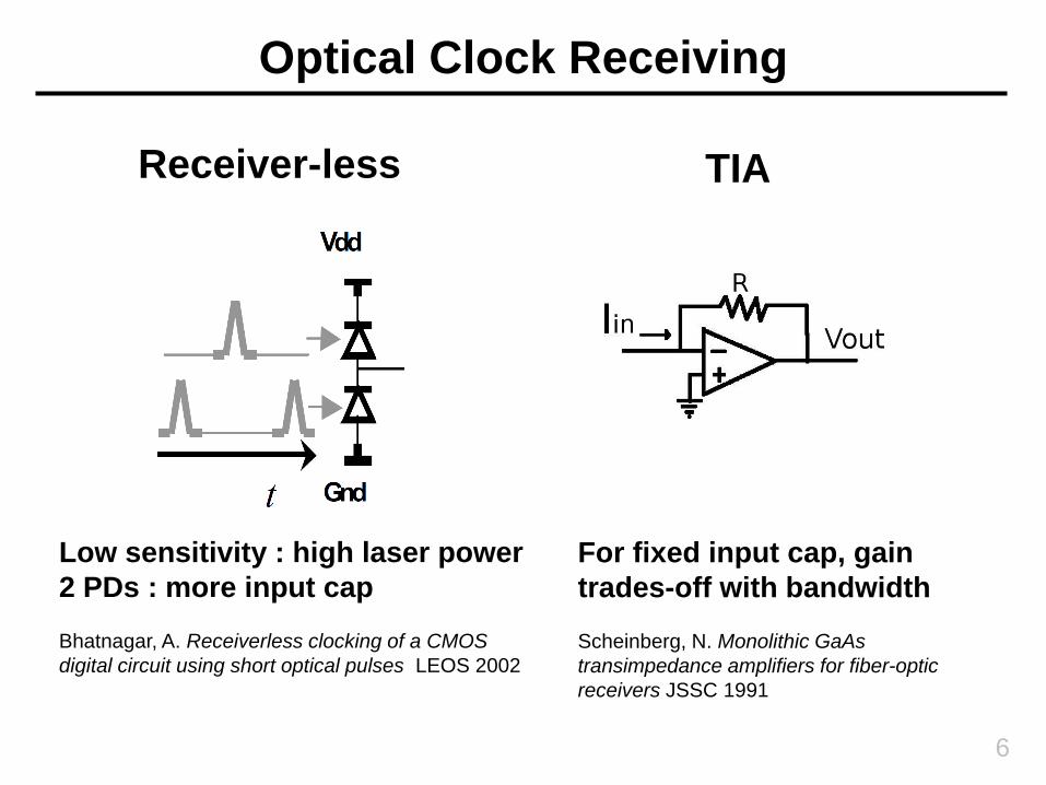
Receiver-less TIA
Low sensitivity : high laser power
2 PDs : more input cap
Bhatnagar, A. Receiverless clocking of a CMOS
digital circuit using short optical pulses LEOS 2002
For fixed input cap, gain
trades-off with bandwidth
Scheinberg, N. Monolithic GaAs
transimpedance amplifiers for fiber-optic
receivers JSSC 1991
Optical Clock Receiving

7
TIA vs. Integrating
• Output voltage change in a given bit-
time is maximized when R is infinite
integrating receiver
• High bandwidth requires low R
R=∞
R=finite
Slope =
I_in/C
Vin
time
R*I_in
(1+A)

8
• High impedance (high sensitivity) when signal arrives
• Low impedance (high bandwidth) for reset
• Differential to reject power supply noise – monolithic
PD allows zero bias
Injection-Locked Topology

9
• Ipd / Cin determines
slope of Vin, clock edge
information
• Vin crosses V0, clock
edge received
Ipd
Vreset
Vin V0
Circuit Operation – sense phase

10
• Edge information
propagates through diff
chain, sets reset high
•Closes switches, pulls
Vin down
Ipd
Vreset
Vin V0
Circuit Operation – reset phase

11
• Vin crosses V0 once
more, after same delay
switches reset low.
• returns to initial state
Circuit Operation – ready phase
Ipd
Vreset
Vin V0

12
Adaptive reset strength to ensure lock and
configurability for different environments
Adaptive locking (auto-tune)

13
• Vauto is at
steady state
when locked,
50% duty
cycle
Ipd
Vreset
Vin
Vauto
V0
Circuit Operation - nominal
HI
LOW

14
• If operation
condition
changes, reset
duty cycle error
is stored onto
Vauto
• In this case,
input duty <50%
weaken DIFF3
Ipd
Vreset
Vin
Vauto
V0
Circuit Operation – duty cycle correction

15
• Vauto adjusts
reset strength
to achieve lock
for varying Ipd
pulse strengths
and duty cycles
Ipd
Vreset
Vin
Vauto
V0
Circuit Operation – duty cycle correction

16
Measurement Setup
• In-situ operation and jitter
measurement
• PD response poor, used electrical
PD emulator circuit for measurements
Clock receiver area
40um x 25um
Sense
Amp
Sense
Amp
Source clock
Reference clock
RxClk clock
Reference clock
MU
X
30
asynchronous reference counter
asynchronous test counter
30
Reference
clock
Dig
ital
Back
en
d
Experiment select

17
Auto vs. no Auto

18
Operation Ranges

19
Jitter Measurement
• Sweep reference clock relative
to source clock to capture
distribution of clock edges
• Measure both source clock and
received clock to derive jitter
added by receiver circuit
Schaub, J.D. On-chip Jitter and Oscilloscope Circuits
Using an Asynchronous Sample Clock ESSCRIC 2008

20
Source Jitter

21
• At 2.5GHz, circuit
jitter added is 1.57ps
• Falling edge jitter is
much larger than
rising edge, since it is
determined by the
duty cycle control
circuit, instead of the
source falling edge.
Jitter Measurement

22
Input Sensitivity
• This clock
receiver topology is
3x more sensitive,
which saves laser
power.
• Assuming same
photodiode used in
both cases.
(Cpd=10fF
and Cwire=5fF)
23
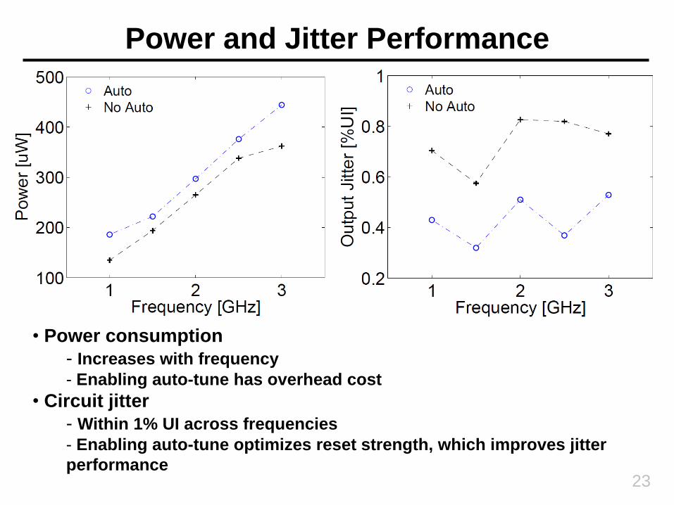
Power and Jitter Performance
• Power consumption
- Increases with frequency
- Enabling auto-tune has overhead cost
• Circuit jitter
- Within 1% UI across frequencies
- Enabling auto-tune optimizes reset strength, which improves jitter
performance

24
Conclusion
• Silicon photonic interconnects are a promising alternative to electrical interconnects – Monolithic Integration : energy-efficiency
– DWDM : bandwidth density
• Injection-locked clock receivers enable efficient clocking solution for DWDM – Break gain-bandwidth trade-offs in TIAs
– High-input sensitivity (low laser power)
– Low clock receiver power
– Key to low data-receiver power
• Adaptive locking improves robustness to process mismatch, input signal variation, and operation condition change
25
Acknowledgements
The work was support in part by MIT CICS, DARPA, NSF, FCRP ICF, Trusted Foundry, Intel, and NSERC.

26
Thank you for your time!