INFLUENCE OF STRESS ON THE PERFORMANCE OF LEAD …
183
The Pennsylvania State University The Graduate School INFLUENCE OF STRESS ON THE PERFORMANCE OF LEAD ZIRCONATE TITANATE THIN FILMS A Dissertation in Materials Science and Engineering by Kathleen Coleman © 2020 Kathleen Coleman Submitted in Partial Fulfillment of the Requirements for the Degree of Doctor of Philosophy December 2020
Transcript of INFLUENCE OF STRESS ON THE PERFORMANCE OF LEAD …

The Pennsylvania State University
The Graduate School
INFLUENCE OF STRESS ON THE PERFORMANCE OF LEAD ZIRCONATE
TITANATE THIN FILMS
A Dissertation in
Materials Science and Engineering
by
Kathleen Coleman
© 2020 Kathleen Coleman
Submitted in Partial Fulfillment
of the Requirements
for the Degree of
Doctor of Philosophy
December 2020
ii
The dissertation of Kathleen Coleman was reviewed and approved by the following:
Susan Trolier-McKinstry
Professor of Ceramic Science and Engineering
Professor of Electrical Engineering
Dissertation Advisor
Chair of Committee
Clive A. Randall
Professor of Materials Science and Engineering
Jon-Paul Maria
Professor of Materials Science and Engineering
Brian Foley
Assistant Professor of Mechanical and Nuclear Engineering
Raul Bermejo
Special Member
Professor of Materials Science and Engineering
Montanuniversität Leoben
John C. Mauro
Professor of Materials Science and Engineering Chair of Intercollege Graduate Degree Program in Materials Science and Engineering
iii
Abstract
Lead zirconate titanate (PbZrxTi1-xO3, PZT) thin films are used in piezoelectric
microelectromechanical systems (PiezoMEMS) such as sensors, actuators, and energy harvesting
devices. The performance of PZT films depends on the piezoelectric response and the structural
integrity of the piezoelectric film. Typically, films are driven to higher fields, stresses, and strain
levels compared to bulk devices. The relationship between these large input signals, particularly
high stresses, and the performance of these films needs to be quantified. This thesis investigates
the influences of various stresses on the properties of PZT films and determines their mechanical
limits.
With small changes in the stress state (~200 MPa), the piezoelectric, dielectric, and
ferroelectric properties of PZT films may be tuned. The dielectric and piezoelectric properties of
0.6 µm thick {001} sol-gel Pb0.99⧠0.01(Zr0.52Ti0.48)0.98Nb0.02O3 (PZT) films on Si substrates and thin
Ni foils were measured as a function of applied strain and total stress. These films are under
different residual stresses arising from thermal expansion mismatch between the film and the
substrate. With no additional applied stress, the remanent polarization, Pr was approximately 21 ±
0.2 µC/cm2 and 39.5 ± 2.3 µC/cm2 for PZT films on Si and Ni, respectively. The higher Pr on Ni
originates from more “c” domains (out-of-plane polarization) due to the compressive stresses. The
link between stress and domain orientation was further explored by applying uniaxial strains. PZT
film on 50 µm Ni foil had uniaxial strains of -0.2% to 0.5% applied, while films on Si were only
exposed to strains between -0.06 and 0.06%, because of substrate failure. When PZT films on Ni
foil were under a 0.5% tensile strain, their Pr decreased by 7-10% and their relative permittivity
increased by ~20% relative to zero applied strain. This trend reversed upon compressive strain. In
addition, the piezoelectric coefficient, e31,f was -9.0 ± 0.45 µC/cm2 and -7.1 ± 0.35 µC/cm2 on Ni
iv
and Si, respectively, and increased in magnitude with applied uniaxial compressive strain. These
changes suggest some ferroelastic reorientation.
The extent of property changes with stress was also shown to differ for the films on Si and
Ni. To explore the relationship between the tunability of properties with residual stress, the PZT
films on Ni and Si were electrically characterized from 15 K up to room temperature. At room
temperature, the dielectric irreversible Rayleigh parameter, αray, was 15.5 ± 0.1 and 28.4 ± 1.6
cm/kV for PZT on Si and Ni, respectively. The higher αray suggests more irreversible domain wall
motion at room temperature, and may be explained by the lower stiffness on the Ni foil reducing
the degree of clamping of these films. Below 200 K, αray for the PZT/Si sample exceeds that of the
PZT/Ni sample. This is believed to arise from differences in the energy landscape of pinning
centers for domain wall motion and was supported by Preisach analysis and the third harmonic
phase angle results.
The second portion of this thesis focuses on understanding the mechanical limits of PZT
thin films. Piezoelectric thin films are vulnerable to fracture, which results in degradation of the
structural integrity and device performance. This work explores the fracture process in
PiezoMEMS, which is a combination of a crack initiation event in the thin piezoelectric film
followed by crack propagation through the subsequent layers. Biaxial bending tests, using the Ball-
on-three-Balls (B3B) technique, were performed on stacks containing Pb(Zr0.52Ti0.48)O3 (PZT) thin
films on thick (500 µm) Si wafers.
First, a series of PZT films of varying thicknesses (i.e. 0.7 µm, 1.3 µm, or 1.8 µm) was
tested using the B3B method to determine the relationship between crack initiation stress and film
thickness. Crack initiation stress increased when the film thickness decreased. PZT films that were
0.7 µm thick required ~590 MPa to initiate a crack, where 1.8 µm thick films required only 490
v
MPa to crack. This trend was modeled using a finite fracture mechanics model that necessitates a
coupled stress-energy criterion for crack initiation in brittle ceramics. In this model, it was shown
that for PZT in this film thickness regime (0.1 to a few microns), the crack initiation stress
depended on the thickness.
At higher loads, the entire stack would fail. First, a fracture would initiate in the PZT film,
enter the LaNiO3 layer, and arrest in the compressive SiO2 layer. With higher loads, the crack
could then propagate through the SiO2 and Si layer, failing the entire stack. Weibull analysis shows
a significant effect of the thin film thickness on the stack’s strength. The characteristic strength
and Weibull modulus were σ0 ~ 1110 MPa and m ~ 28 for the stacks with the 0.7 µm thin PZT
film stack, σ 0 ~ 1060 MPa and m ~ 26 for the 1.3 µm film stack, σ 0 ~ 880 MPa and m ~ 10 for the
1.8 µm film stack. This trend in crack propagation was rationalized using linear elastic fracture
mechanics indicating the importance of the PZT layers thickness on the initial crack length and
the stack’s strength.
Since films are typically under electromechanical loading conditions, electromechanical
failure was also explored by investigating the relationship between the direction of applied stress
and failure pattern. Cracks consistently propagated perpendicular to the maximum tensile stress
direction and connected thermal breakdown events, suggesting correlations between electrical and
mechanical failure. Additionally, the influence of electric history on the crack initiation stress was
also determined using the B3B method. Electrical fields are important for enhancing the properties
of piezoelectric thin film, but in this thesis, have been shown to decrease the mechanical load the
films can withstand. For 1.6 µm thick PZT films, the crack initiation stress was reduced by ~15%
when it was poled or under a DC bias compared to a virgin film. This may be due to a reduction
in domain wall motion when poled, or development of local strain from some ferroelastic domain
vi
reorientation with an applied field.
Overall, residual stress in PZT thin films was shown to influence the properties; at lower
applied stress level these properties can be tuned. At higher stresses (around 500 MPa), cracks
initiate in the PZT films and the thickness and the electrical history of the PZT layer affects the
crack initiation stress. At stress levels greater than 800 MPa, failure was observed in the multilayer
stack, as the crack that initiated in the PZT layer would then propagate through the underlying
layers. These trends observed in this thesis will allow for further commercialization and improved
performance of thin films. Additionally, the methods, models, and calculations used in this study
can be expanded to other piezoelectric thin films, brittle ceramic coatings, and multilayers stacks.
vii
Table of Contents
List of Figures .............................................................................................................................x
List of Tables ...........................................................................................................................xvi
Acknowledgements ................................................................................................................ xvii
Chapter 1. Motivation and Thesis Organization .......................................................................1
1.1 Ferroelectric Thin Film Applications .............................................................................1
1.2 Factors that Influence Performance ...............................................................................2
1.3 Dissertation Overview ...................................................................................................3
Chapter 2. Introduction and Background .................................................................................5
2.1 Piezoelectricity .............................................................................................................5
2.2 Pyroelectricity ...............................................................................................................7
2.3 Ferroelectricity ..............................................................................................................7
2.4 Nonlinearity ................................................................................................................ 11
2.4.1 Rayleigh Law ....................................................................................................... 12
2.4.2 Preisach Analysis ................................................................................................. 14
2.5 Pb(Zr, Ti)O3 Systems .................................................................................................. 17
2.5.1 PZT thin films ...................................................................................................... 20
Chapter 3. Effect of Stresses on the Dielectric and Piezoelectric Properties of
Pb(Zr0.52Ti0.48)O3 Thin Films ..................................................................................................... 22
3.1 Introduction ................................................................................................................ 22
3.1.1 Types of Stresses ................................................................................................. 23
3.1.2 Overview ............................................................................................................. 27
3.2 Experimental Procedure .............................................................................................. 27
3.2.1 PZT Chemical Solution Deposition ...................................................................... 27
3.2.2 Film Structural Characterization........................................................................... 30
3.2.3 Film Electrical Characterization ........................................................................... 31
3.2.4 Methods for Applying Uniaxial Strains ................................................................ 33
3.2.5 Piezoelectric Coefficient (e31,f) Measurement ....................................................... 34
3.3 Results ........................................................................................................................ 35
3.4 Discussion................................................................................................................... 43
3.5 Conclusions ................................................................................................................ 47
viii
Chapter 4. Extrinsic Contributions to the Dielectric and Pyroelectric Properties of
Pb0.99[(Zr0.52Ti0.48)0.98Nb0.02]O3 Thin Films on Si and Ni Substrates .............................................. 48
4.1 Introduction ................................................................................................................ 48
4.2 Experimental Procedure .............................................................................................. 52
4.3 Results and Discussion: ............................................................................................... 54
4.4 Conclusions ................................................................................................................ 72
Chapter 5. Thickness Dependence of Crack Initiation and Propagation in PZT/Si Stacks ...... 73
5.1 Introduction ................................................................................................................ 73
5.1.1 Weibull Statistics for Failure ................................................................................ 75
5.1.2 Fracture Mechanics .............................................................................................. 76
5.1.3 Overview ............................................................................................................. 78
5.2 Experimental Procedure: ............................................................................................. 78
5.2.1 Sample Preparation and Structural Characterization ............................................. 78
5.2.2 Ball on Three Ball Biaxial Test Method ............................................................... 79
5.3 Results ........................................................................................................................ 82
5.3.1 Microstructure ..................................................................................................... 82
5.3.2 Strength distribution ............................................................................................. 83
5.3.3 Crack initiation .................................................................................................... 85
5.3.4 Crack propagation ................................................................................................ 87
5.4 Discussion................................................................................................................... 88
5.4.1 Residual stresses .................................................................................................. 88
5.4.2 Weibull volume effect .......................................................................................... 88
5.4.3 Model for crack initiation: Finite Fracture Mechanics .......................................... 90
5.4.4 Model for crack propagation: Linear Fracture Mechanics ..................................... 92
5.5 Conclusions ................................................................................................................ 95
Chapter 6. Effect of Electromechanical Loads on Failure Limits of PZT thin Films .............. 97
6.1 Introduction ................................................................................................................ 97
6.2 Influence of Uniaxial Strains on Electromechanical Failure ......................................... 99
6.3 Influence of Electrical History on Failure of Lead Zirconate Titanate Thin Films ...... 103
6.3.1 Experimental Details .......................................................................................... 104
6.3.2 Results and Discussion ....................................................................................... 107
6.4 In situ property measurements under electromechanical loads ................................... 117
6.5 Conclusions .............................................................................................................. 119
ix
Chapter 7. Conclusions and Future Work ............................................................................ 121
7.1 Conclusions .............................................................................................................. 121
7.2 Future Work .............................................................................................................. 125
7.2.1 Structural characterization of films under strain ................................................. 125
7.2.2 Determine the fracture toughness of PZT thin films ........................................... 129
7.2.3 Investigate differences in defect chemistry ......................................................... 133
7.2.4 Investigate relationship between strain and aging rates ....................................... 134
7.2.5 Additional applications ...................................................................................... 134
References .............................................................................................................................. 137
Appendix ............................................................................................................................... 156
x
List of Figures
Figure 2-1 Polarization-Electric field (P-E) hysteresis loop from a lead zirconate titanate sample.
The remanent polarizations (+Pr and -Pr) are defined as the net polarization remaining in the sample
when field is removed, and the coercive fields (+Ec, and -Ec) are the fields required to return the
polarization to zero. (a)-(e) show schematics of the domain structure at various points on the
hysteresis loop. The domain structures shown are for an appropriately aligned single crystal. .....9
Figure 2-2. Energy landscape for pinning centers vs. position of domain wall. (a) shows an
example of reversible domain wall motion where the domain wall is fully pinned to one potential
well, and (b) shows irreversible domain wall motion where the domain wall can overcome the
barrier height and move. Pinning sites are denoted by X. ........................................................... 12
Figure 2-3. A schematic representation of the Preisach distribution on an α vs ß plot (otherwise
known as the Preisach plane). At four points on the plot the hysteron’s P-E loops are represented
schematically. The color bar (far left) represents the intensity at each (α, ß) point, where the red
circles is the highest intensity and blue is the lowest in this schematic example. ........................ 14
Figure 2-4. FORC reversal curves (a) showing the various minor P-E loops of a PZT film. (b-e)
shows the Preisach hysteron distribution for PZT at a given field based on the field applied to the
sample. The light and darks shades of the hysteron distribution represent upward and downward
polzarization directions for the hysteron, respectively. The legend of circle colors from blue up to
red represent increasing number of hysterons with the various values of α and ß. ...................... 16
Figure 2-5. Crystal structure schematics of the cubic perovskites phase (a) Where the A site atoms
site on the corners (in this case dark bue atom), the B site sites in the center of the unit cell (light
blue) and the X site on the center of the faces (red). (b) shows the derivative ferroelectric tetragonal
phase where the B ion moves towards one of the X site atoms, elongating the cell in this polar
direction. (c) shows the rhombohedral phase derivative where the center Ti atom moves along the
body diagonal towards three of the X atoms. ............................................................................. 18
Figure 2-6. Phase diagram of PbZrO3-PbTiO3. C denotes the paraelectric cubic phase, O denotes
Orthorhombic, R denotes rhombohedral, T denote tetragonal, M denotes monoclinic, and MPB is
for the morphotropic phase boundary. Figure is adopted from: [33,60–62] ................................ 19
Figure 3-1. Method for applying uniaxial strains on PZT films. The radius of curvature method
(a) was used for higher strains and more flexible substrates, and the beam bending method (b) was
used for lower strains for the Si case. ........................................................................................ 27
Figure 3-2.Various microstructures that may form depending on the lead environment of the Pb
furnace and PbO added to the film. (a) lead deficient film with a fine-grained surface pyrochlore
phase which nucleated at the grain boundaries of PZT. This film requires a PbO layer. (b) pure
PZT phase, after deposition of a PbO capping layer (c) PZT phase with a Pb-rich secondary phase
on top that can be removed in acetic acid................................................................................... 30

xi
Figure 3-3. XRD patterns of the substrate and subsequent layers prior to the addition of the PZT
layer. Peaks for the Si and LNO for the Si substrate (a) and peaks for the Ni, HfO2 buffer and LNO
for the flexible Ni substrate (b) are labeled. ............................................................................... 31
Figure 3-4 Photo taken of the Ni foil sample being wrapped around a mandrel with a radius of 4.8
mm............................................................................................................................................ 33
Figure 3-5. Schematic set up for measuring e31,f on Ni foil; the glass slides are adhered to the
cantilever to allow the sinusoidal strain to reach the measured area. .......................................... 35
Figure 3-6 XRD patterns for 0.6 µm thick PZT films on Si (a) and Ni (b), and top surface FeSEM
images of the grain structures on Si (c) and Ni (d), and FeSEM cross section for the 500 µm thick
Si wafer (e) and 50 µm thick Ni foil (f). The Lotgering factors were 98% for the sample on the Ni
foil and 92% for the sample on Si. ............................................................................................. 36
Figure 3-7. The relative permittivity vs temperature measured at various frequencies (from 200
Hz up to 140 kHz) for PZT on Ni (a) and PZT on Si (b). The temperature when the derivative
equals zero was assigned to be Tc for the two films. Tc for PZT on Ni and Si were around 320°C
for both films. ........................................................................................................................... 37
Figure 3-8. P-E hysteresis loops for PZT on Ni (red), and PZT on Si (green). The Pr for films on
Si was 21 ± 0.2 µC/cm2, while films on Ni had Pr of 39.5 ± 2.3 µC/cm2. This was due to the
compressive thermal expansion stresses for PZT films on Ni, causing a larger percentage of “c”
(out-of-plane) domain orientation [18]. ..................................................................................... 38
Figure 3-9 Polarization hysteresis loops for PZT films on Si (Panel Ia) and Ni (Panel IIa).
Changes in Pr as a function of applied compressive and tensile strain on Si (Panel Ib) and Ni (Panel
IIb) as well as the linear trend of the normalized change in Pr [e.g. Pr(strain)/Pr (zero strain)] as a
function of both applied compressive and tensile strain on Si (Panel Ic) and Ni (Panel IIc). The
strain range for samples on Ni was -0.2% strain to 0.4% strain; for Si it was from -0.06% to 0.06%.
The purple dotted lines (Panel Ic & Panel IIc) indicate the smaller strain range over which films
on Si were tested. Negative strains represent in-plane compressive strains, and positive represent
in-plane tensile strain. ............................................................................................................... 40
Figure 3-10 Permittivity as a function of strain and AC field for the PZT on Ni foil (a) and the
normalized permittivity as function of strain at 5 kV/cm AC field (b). Both εinit and αRay increased
as a function of tensile strain. These measurements were at 0 V DC bias. .................................. 42
Figure 3-11 (a) Normalized e31,f as a function of applied strain for PZT on Si. The magnitude of
the e31,f increases linearly under compression. (b) Normalized e31,f with various applied DC biases
as a function of compressive strain. m indicates the slope of the linear fit of the normalized e31,f as
a function of strain (%); the stain dependence was larger when samples were repolled while under
strain. ........................................................................................................................................ 43
Figure 3-12. Schematic of the domain state for the films on Si substrates (a) and Ni foil (b, c).
Also shown is how an applied compressive stress could affect the domain state on Si (a) and Ni
(c), as well as how tensile stress might change the domain state for the samples on Ni (b) [72]. Red
arrows facing in (→ ←) represent compression. Blue arrows facing outwards (← →) represent

xii
tension. Black triangles (►◄) in between domains represent local stresses induced from non-180º
domain switching. ..................................................................................................................... 45
Figure 3-13. Working total stress ranges for the films on the two substrates. The difference of
these working ranges slightly affects the slope of the properties changes as a function of stress, as
well as the complexity of the domain structure in these films on different substrates. Data for this
plot comes from the experiments shown in Figure 3-9. ............................................................. 47
Figure 4-1. P-E hysteresis loops for PZT on Ni (a) and Si (b). The remanent polarization (c) and
coercive field (d) as a function of temperature for PZT on Ni (red squares) and on Si (green circles).
The Ec for PZT on Ni was roughly twice that of PZT on Si for all temperatures measured. ........ 55
Figure 4-3. Estimated Pr values from phenomenology at 15 K (blue) and 296 K (pink) based on
the percentage of “c” domains (a), and the observed Pr for PZT samples on Ni and Si. .............. 56
Figure 4-4. Third harmonic phase angle, δ3, for PZT on Ni (a) and on Si (b) from room temperature
down to 10 K. The field (Eδ3), where the phase angle reached -90 ±5° is used as a proxy for
defining when Rayleigh-like behavior was present. As the temperature decreases, Eδ3 increases.
This temperature dependence is shown to be greater for PZT on Ni as seen by the larger electric
field required to reach a -90° phase angle. ................................................................................. 58
Figure 4-5. The Eδ3vs. coercive field for PZT on Ni (red square) and Si (green circle). From the
slope (m) of these lines, it is estimated the Rayleigh regime begins around 9-14% of the coercive
field for both PZT on Si and for PZT on Ni. .............................................................................. 59
Figure 4-6. Permittivity as a function of electric field within the Rayleigh regime for (a) Ni and
(b) Si samples. Rayleigh parameters of εinit (c) and αray (d) were plotted as a function of
temperature for PZT films on both Ni (red squares) and Si substrates (green circles). Note: 296K
(i) indicates the permittivity values at room temperature at the start of the experiment and 296 K
(f) indicates the values at room temperature after the experiment. The lack of clear differences
indicates that the sample had minimal aging through the experiment. ........................................ 60
Figure 4-7. αRay/εinit ratio for PZT on Ni (red squares), and on Si, (green circles). ..................... 62
Figure 4-8. Arrhenius plot of the natural log of αray vs 1/T to determine the ranges of activation
energies for irreversible domain wall motion for PZT on Ni (red circle) and PZT on Si (green
square). From the slope the calculated activation energy at higher temperatures (from a linear fit
form 225K to 296K) PZT on Ni and Si was 32.4 ± 3.2 meV and 16.9 ± 1.1 meV, respectively. . 63
Figure 4-9. FORC loops for PZT films on Ni at 296 K, 225 K, 150 K, 75 K, and 15 K. The field
range was from -4Ec to +4Ec for each temperature. .................................................................... 64
Figure 4-10. FORC loops for PZT films on Si at 296 K, 225 K, 150 K, 75 K, and 15 K. The field
range was from -4Ec to +4Ec for each temperature. .................................................................... 65
Figure 4-11. Reversible FORC data, Prev for PZT films on Ni (a) and PZT films on Si (b). The Prev
for PZT on Si was 2-3 times larger than PZT on Ni. .................................................................. 66

xiii
Figure 4-12. Pirrev for PZT on Ni at 296 K (a), 225 K (b), 150 K (c), 75 K (d), 15 K (e). Alpha and
Beta are normalized to 4 times Ec at the reported temperature. .................................................. 67
Figure 4-13. Pirrev for PZT on Si at 296 K (a), 225 K (b), 150K (c), 75 K (d), 15 K (e). Alpha and
Beta are normalized to 4Ec at the reported temperature. ............................................................. 68
Figure 4-14. Schematic of distribution of the population of hysterons with certain pinning energies
for PZT on Ni (dashed red curve) and Si (solid green curve). The vertical dashed black line
represents the available energy at a given temperature. Any pinning center with lower energy levels
is anticipated to be overcome at that temperature. ...................................................................... 70
Figure 5-1. Schematic of the samples where PZT of varying thicknesses is grown on top of Si
wafer. ........................................................................................................................................ 79
Figure 5-2. Schematic of the Ball on three Ball (B3B) setup. .................................................... 80
Figure 5-3. XRD pattern of the 0.7 µm PZT (a), 1.3 µm PZT (b), and 1.8 µm PZT on Si (c), where
the Lotgering factor is above 0.96 for all samples. The microstructure top view and cross section
of the 0.7 µm (d and g respectively), 1.3 µm (e and h respectively), and 1.8 µm PZT sample (f and
i respectively). The average grain size (diameter) of the 0.7 µm, 1.3 µm, and 1.8 µm PZT film is
86 ± 7 nm, 105 ± 20 nm, and 106 ± 14 nm, respectively. ........................................................... 82
Figure 5-4. The Weibull plot for the following samples: SiO2/Si (blue circle), 1.8 µm PZT on
LaNiO3/SiO2/Si (red square), 1.3 µm PZT on LaNiO3/SiO2/Si (orange downward triangle), and
0.7 µm PZT on LaNiO3/SiO2/Si (green upward triangle). The Weibull strength and Weibull
modulus varied with the thickness of the PZT film on the Si wafer............................................ 84
Figure 5-5. Dark field optical microscope images of 0.7 µm film (Panel I), 1.3 µm film (Panel II),
and 1.8 µm film (Panel III) loaded between 40% and 80% of the characteristic strength. Initial
cracking was observed at loads of 64 N and higher for the 0.7 µm film, 56 N and higher for the 1.3
µm film, 49 N and higher for the 1.8 µm films. This corresponds with approximately 590 MPa,
535 MPa, and 490 MPa of stress in the PZT layer. .................................................................... 86
Figure 5-6. FIB cross section of the 1.8 µm PZT film’s initial cracking (a) and the 0.7 µm PZT
film’s initial cracking (b). The crack propagates through the PZT layer and the LNO and ends at
the SiO2 layer. Initial cracks through the PZT and LNO layer were observed on multiple samples
of varying stresses and PZT thicknesses. The faint line below the crack at the SiO2 layer is an
artifact of the FIB preparation. .................................................................................................. 87
Figure 5-7. Calculated relationship between crack initiation stress and the thickness of the PZT
layer using the Weibull volume effect compared to the experimental data. Black squares represent
the characteristic crack initiation stress, and the dashed lines are calculated, using the crack
initiation stress of the 0.7 µm thick PZT layer as a reference. The various colors represent
estimations using different Weibull moduli for PZT for each calculation. .................................. 90
Figure 5-8. Comparison of the strength as a function of thickness for the observed trends (gray
squares), and finite fracture mechanics model predictions (KIc=0.6, KIc=0.8, and KIc=1.0, are the
green solid line, blue dot-dash line, and purple dotted line, respectively). The observation of this
xiv
thickness dependence follows the finite fracture mechanics model for thicknesses larger than 1µm,
however it fails for very thin films. This may be due to domain wall contributions, which are not
taken into account in the model. ................................................................................................ 91
Figure 5-9. Apparent toughness of the multilayer stack as a function of the crack length, the
residual stress, and thickness of the PZT layers. ........................................................................ 94
Figure 6-1. Optical images of the failure behavior of 600 µm diameter Pt electrodes on 0.6 µm
PZT thin films. The electrodes were under -0.051% (a), -0.036% (b), 0.00% (c), 0.02% (d), 0.03%
(e), and 0.051% (f) uniaxial strain in the y direction. The arrows represent the direction
perpendicular to the maximum tensile stress direction, which also indicates the cracking direction.
The larger arrows represent a larger magnitude of the tensile stress. Thermal breakdown events
(black dots) decorate the cracks, giving distinct failure patterns based on the applied uniaxial
strains. .................................................................................................................................... 100
Figure 6-2. SEM of the top surface a failed capacitor, showing both crack and thermal breakdown
events for a PZT film under 0% applied strain (a), and -0.05% uniaxial strain (b). Cracks connect
the thermal breakdown events as shown by the arrows. The yellow dashed arrows represent cracks
that would have occurred after the thermal breakdown events as the crack cuts through the thermal
breakdown event. The solid orange arrow represents a crack that occurred before the breakdown
events it connects. The crack propagates perpendicular to the maximum tensile stress direction as
shown in (b). ........................................................................................................................... 102
Figure 6-3: The B3B setup, showing the 4 balls and the specimen in the middle, as well as the
structure of the samples from the 12 x12 mm2 specimen. A Pt electrode (gray) is deposited on the
PZT top surface (orange layer) to enable contact to the center of the specimen. It consists of a
circle with a diameter of 1 mm in the center, a 100 µm wide trace and a 400 µm x 400 µm square
close to the edge. A cross section showing each layer in the stack is also depicted (not to scale).
............................................................................................................................................... 105
Figure 6-4: (a) Top view SEM image showing the grain size of the PZT layer. (b) Cross sectional
SEM image showing the layered structure of the 1.6 µm thick PZT layer, as well as the platinum
bottom electrode...................................................................................................................... 108
Figure 6-5: XRD pattern of the PZT layer, showing random orientation. The symbol “*” indicates
background peaks from the substrate. ...................................................................................... 108
Figure 6-6: Relative permittivity as a function of AC signal for the virgin (green upward triangle),
poled (red square), and under DC bias (orange downward triangle) films. The linear Rayleigh
regime is denoted between the two vertical dashed lines and was consistent for all the films. .. 109
Figure 6-7: Polarization electric field hysteresis (PE loops) for the virgin (green solid lines), poled
(red dotted line), and under DC bias (orange dashed line) samples. ......................................... 110
Figure 6-8: Schematic illustration of the domain structure for the virgin (green), poled (red) and
under DC bias (orange) sample. Arrows represent the polarization direction for the respective
domains. ................................................................................................................................. 111
xv
Figure 6-9: Probability of failure versus failure stress in a Weibull diagram for the three samples:
virgin (green upward triangle), poled (red square) and under DC bias (orange downward triangle)
and the Pt/Si sample (blue circles), as a reference. ................................................................... 113
Figure 6-10: FIB image showing the crack stop at the interface of the PZT and Pt seed layer
beneath. The image was prepared using a FEI Scios Focused Ion Beam (FIB) system. The porosity
in the SiO2 layer may be due to lead diffusion through the stack, and some damage from the FIB.
............................................................................................................................................... 115
Figure 6-11: Change in normalized relative permittivity (a) and change in loss tangent (b) as a
function of the load force during the B3B measurements. The three regions can be allocated to
three different conditions, governing the electrical properties of the PZT layer. Region I is the
preload region. Region II is the regions before cracks are observed and Regions III is the regions
after cracks were observed on the surface. Each of the three lines represent a separate sample
tested....................................................................................................................................... 118
Figure 6-12: Normalized change in the relative permittivity as a function of time (log) to
determine the aging rate after the removal of a mechanical load. The dielectric aging rate was 1.2%
per decade. .............................................................................................................................. 119
Figure 7-1. a) Raman spectra on Ni foil under different strain levels. The inset shows changes in
Ipeak 6Ipeak 4 as a function of applied strain level (b) Peak 4 corresponds to the 400 cm-1 Eg
LNO peak. Peak 6 corresponds with the E(LO3) and the A1(LO3) PZT mode, which is dependent
on the domain structure and the relative intensity decreases with a higher number of “c” domains.
............................................................................................................................................... 128
Figure 7-2. A schematic of the proposed nanofabrication of a series of released PZT thin film
beams. (a) shows a schematic cross section of the as grown PZT layer (purple) on the LNO layer
(green), on SiO2 (yellow) and Si (gray) and a top view. (b) shows the first etches to create pits
down through the Si layer. (c) shows the undercut of the Si layer which would release the PZT
cantilever beams. The top view has white tick marks to represent the region that has been released.
............................................................................................................................................... 131
Figure 7-3. SEM cross section of the first generation of the nanofabricated PZT cantilevers. The
cantilevers had SiO2 ledge around the PZT layer leading to incorrect strength and fracture
toughness measurements of the PZT layer. .............................................................................. 132

xvi
List of Tables
Table 5-1. Characteristic load, characteristic strength, and Weibull modulus for the PZT/Si stacks
of various thicknesses and the Si substrate. All stress values are in MPa and are calculated for the
stress in the Si layer upon failure. Brackets represent 90% confidence intervals. ....................... 84
Table 5-2. In-plane residual stresses calculated in each of the layers. ........................................ 88
Table 5-3. Reported mechanical properties and averaged thermal expansion coefficients of the
various layers in the stack [18,93,96,112,114,189,190]. ............................................................. 94
Table 6-1. Calculated stresses in the x and y direction for films represented in Figure 6-2 a-f. For
σp, the piezoelectric coefficient, e31,f was estimated to be -7.1±0.35 C/m2. Numbers in bold indicate
the maximum tensile stress for the sample. To calculate the applied stress in the x (σa,x) direction
the Poisson’s ratio of 0.3, and Young’s modulus of 90 GPa for (001) oriented PZT was used [93].
Values are in MPa unless otherwise noted. .............................................................................. 103
Table 6-2. Table of the calculated figure of merits (FoM) for the various applications for sensors,
actuators and energy harvesting devices. ................................................................................. 112
Table 6-3: Weibull modulus, m, and characteristic strength, 0, for failure of the difference sample
stacks. Values in [] represent the 90% confidence interval. ...................................................... 114
Table 6-4. Calculated stresses (applied, piezoelectric, and residual stresses) in the PZT films and
total stress for crack initiation for each film based on its electric history. There is an additional
systematic error of the residual stress and crack initiation stress of ± 30 MPa. ......................... 116
Table 7-1. List of the PZT and LNO modes corresponding to the peaks in Figure 7-1 [205,212].
............................................................................................................................................... 128
xvii
Acknowledgements
First of all, I would like to thank my advisor, Professor Susan Trolier-McKinstry. She has
invested a tremendous amount of time in me during my studies at Penn State. I met Dr. Trolier-
McKinstry at the Penn State open house and from her presentation and our conversations, I realized
she was a caring, dedicated, hardworking, and humble professor. These qualities make her an
incredible scientist and mentor. She has helped me over the course of this Ph.D. by challenging
me, teaching me, encouraging me, and supporting me. I would not have flourished without her. I
will always strive to be as sincere, dedicated, and thorough in my career as she is. Thank you Dr.
McKinstry—it has been a true pleasure learning and working with you.
Secondly, I would like to thank my committee member, Raul Bermejo. Raul visited Penn
State during my second year of graduate school, and after his colloquium talk, we had lunch and
discussed ways that we could collaborate. Raul taught me the fracture mechanics of ceramics,
stress-energy coupled criterion for crack initiation, the ball on three ball (B3B) test, and linear
elastic fracture mechanics. In addition, Raul invited me to work at the Institute for Structural and
Functional Ceramics at the University of Leoben. Raul, Eva, and their three kids (Nora, Emil, and
Theo) gave me a very warm welcome as I arrived in Austria. Thanks, Raul, for taking me on and
teaching me a lot even from abroad.
In addition, I would like to thank my extremely knowledgeable and approachable
committee. First, Clive Randall, who would often stop by my desk to discuss my CDP project. He
suggested books and ideas to explore, which was always a delight. After my candidacy exam, he
offered to teach me a course on the fundamentals of ferroelectrics to help me make the bigger
connections. These discussions both in MSC and Liberty helped me develop the fundamentals, but
also made me think about connections to other areas of materials science. I would also like to thank

xviii
Brian Foley, who even back at the 2017 ISAF conference was excited to discuss research and
collaborate. I also thank Jon-Paul Maria who taught me an excellent course on electroceramics.
He is an excellent instructor and helped me make bigger connections. Both JP and his group have
been very approachable, and helpful.
In addition to my committee, I would like to thank Julian Walker, who was a postdoctoral
scholar in the STM group for my first two years in graduate school. He guided me through the
initial ropes of our Center for Dielectrics and Piezoelectrics (CDP) project. Julian would stay late
in the cleanroom and give up weekends to help me reach deadlines. He always answered my
knocks to his door to fix equipment, discuss good or bad results, and answer my questions. He also
would discuss my future career and find good collaborators for our project. Being able to go to
Julian’s office made everything those first few year more manageable and helped me enjoy this
research.
I would also like to acknowledge and thank several collaborators on this work. First
Brendan Hanrahan, who approached me after a CDP meeting to try measuring pyroelectric
coefficients on PZT on Ni and Si. He taught me about pyroelectricity and phenomenology, and
this led to a nice study. Secondly, I would like to thank Maximillian Ritter, who was a fantastic
master student in Leoben, who came to Penn State to execute several B3B studies with me. It was
a great summer being able to work with you. I would also like to thank the entire ISFK (particularly
Josef Kreith, Robert Danzer, Peter Supancic, Irena Kraleva, and Walter Harrer) and the ESI
(Markus Alfreider, and Daniel Kiener) for their help when I visited the University of Leoben. In
addition, I would like to thank Dominique Leguillon who help us model several crack-initiation
studies for PZT films, which complemented our experimental results quite nicely. I would also
like to thank Herb McKinstry for helping update the model for the Preisach data. I would also like

xix
to thank Dr. Sukwon Choi, James Lundh, and the rest of Dr. Choi’s group at Penn State for
collaboration on temperature studies of PZT films using thermoreflectance, Raman and IR
imaging. In addition, I would like to thank Thomas Beechem, Max Wetherington, and Marco
Deluca for help with Raman studies of PZT thin films.
I am very grateful for the past and present Susan Trolier-McKinstry group members.
Because of Dr. McKinstry’s standards and dedication, the entire group works together to help each
other attain their research goals. In particular I would like to thank Wanlin Zhu for always helping
with electrical measurements and processing. Lyndsey Denis for teaching me Rayleigh behavior
and reading my drafts. Carl Morandi for teaching me how to use several pieces of equipment in
the electrical lab. Hong Goo Yeo for teaching me how to make PZT on Ni foil (it’s tricky). I would
also like to thank Smitha Shetty for showing me how to use the Lakeshore probe station and for
her brilliant help with analysis on higher harmonics studies. I would like to thank Betul Akkopru-
Akgun as my CDP travel buddy and friend, who has helped me with crystal chemistry and defect
chemistry. I would like to thank Chris Cheng for being a fantastic cube mate and friend. He was
always there with dumplings, cookies, PSU Creamery chocolates, or Sower’s pretzels when I was
stressed. (It’s a good thing we both run). I would like to thank Dixiong Wang and Nicole Hall who
helped me a lot with TAing in crystal chemistry and for being great friends. I would also like to
thank Tianning Liu, who is a supportive friend and she made a great cleanroom and lunch buddy.
I would like to thank Sandie Elder, who has scheduled many meetings, conference rooms and help
me with the logistics and reimbursements for the many conferences. I would also like to thank
Veronika Kovacova, Runar Dahl-Hansen, Juliette Cardoletti, Nathan Bishop, Shruti Gupta,
Michael Hahn, Sanshiro Aman, Leonard Jacques, Son Won Ko, Jung In Yang, Ryan Keech, Travis
Peters, Daisuke Hama, Pannawitt Tipsawatt, and Donovan Moses. I have had lots of great
xx
discussions with them and they have all been excellent co-workers, friends, and this group dynamic
made all the difference.
I would also like to thank the MRI nanofabrication staff. In particular, I would like to
acknowledge Beth Jones for teaching me to make PZT samples, answering my questions, and for
all of our pleasant conversations and laughs. Guy Lavallee for a tremendous help in making nearly
impossible samples for me while I was in Austria and training me on several etch tools. I know I
was “trouble”. I would also like to thank Mike LaBella and Kathy Gehoski who helped with the
lithography of these challenging samples. I would also like to thank Kathy for driving me home
when I became extremely sick in the cleanroom one day. I would also like to thank Bill Drawl,
Bangzhi Liu, Shane Miller, Andy Fitzgerald, and Bill Mahoney for training me on several pieces
of equipment. They always encouraged me even if I was timid and answered my questions. I also
enjoyed all of our conversations in the gowning room. I would also like to thank the material
characterization staff. In particular, I would like to thank Nichole Wonderling, Gino Tambourine,
Maria Dicola, Manuel Villalpando, and Tanner Mengle for their help. In the electrical
characterization lab, I would like to thank Jeff Long for always checking equipment and explaining
some basic electrical circuitry to me. He also would generously lend me expensive pieces of
equipment that I have dragged around campus for various experiments. I would also like to thank
Dr. Libby Kupp, and Sarah Eichfeld for additional help with experiments, equipment, and lab
safety.
I would also like to acknowledge the larger MRI community, the CDP community, and the
Materials Science and Engineering Department at Penn State, where everyone has been willing to
collaborate and despite being in different groups and even different buildings, and in the case of
CDP, different universities, countries, and companies. In particular I would like to thank Hayley

xxi
Coley, the MatSE graduate coordinator as well as Joanne Aller and Brenda Gainey, the CDP
administrative assistants. I would also like to thank many graduate students, and post docs, who
all have helped me in one way or another complete this thesis and my Penn State journey. Thank
you: Timothy Walter, Nisha Sheth, Kayla Cooley, Jess Kopatz, Thorsten Bayer, Jason Lapano,
Jared Carter, Lisheng Gao, Kosuke Tsuji, Mike Vecchio, Mengxue Yuan, Jiawei Luo, Nate Martin,
Ama Agyapong, Beecher Watson, Tom Nigl, Alex Wilson-Heid, Joseph Roth, Alex Molina, Hari
Padmanabhan, Sun Hwi Bang, and many others.
I would also like to acknowledge those that have not directly invested in this research but
my growth as a materials scientist, engineer, and researcher. I would first like to thank many
friends and mentors from UConn (Sam Brown, Megan Gauer, Laura Wilcox, Emily Bousaada,
Aliya Carter, Jess Guerrera, Tori Radovic, and Christine Doherty), and the Institute for Material
Science (Avi Dongare, Rainer Hebert, Radenka Maric, and Bryan Huey). I would like to
acknowledge the UConn Engineering diversity and outreach center, the Bridge program, and
especially the director Kevin McLaughlin who invested so much in me and helped me become a
confident and understanding leader and engineer. Thank you all for supporting me through this
graduate school journey from afar.
Last but far from least, I would like to thank my family— especially my parents, my brother
Michael, my sister Maryanne, my Granny Nonie, and my Grandma Sammon. My dad was the first
person to encourage me to consider engineering and every morning as I walked to school, he would
always be sure I had a ham sandwich and weather permitting a snowball. My family has always
encouraged me regardless of how much they understood and have been there in all the ups and
downs. My mom, my Grandma Sammon, and my Granny were my first teachers. My grandmothers
have always been role models and they worked hard and gave up so much, which has allowed me
xxii
to have this opportunity. I’ll never forget my Grandma Sammon’s math lessons, where I could not
leave the table until I recited my times tables as fast as she could ask them. She was persistent and
said math was so important and her favorite subject. Despite the aggravating lessons and tears,
math has always been my favorite too. While she will never see this work, she is always with me
and for the rest of my life I will “strike the nail a’right” and “give to the world the best I can.” I
can only hope she would say “go maith” to the work in this thesis, as if we finished a math lesson.
Thank you.
This manuscript is based on work supported by the National Science Foundation, as part of the
Center for Dielectrics and Piezoelectrics under Grant Nos. IIP-1361571, IIP-1361503, IIP-
1841453, and IIP-1841466.
Note: The findings and conclusions in this thesis do not necessarily reflect the view of the funding
agency.

1
Chapter 1. Motivation and Thesis Organization
This chapter outlines the motivation for the work described in this thesis and the contents of the
following chapters. Section 1.1 gives a brief overview of various applications of thin film
ferroelectrics. Section 1.2 defines various metrics used to assess the performance of several thin
film devices. Section 1.3 gives a short overview of the work done in the following chapters.
1.1 Ferroelectric Thin Film Applications
Ferroelectric thin films are utilized in various devices, including piezoelectric
microelectromechanical systems, also called piezoMEMS (sensors, actuators, and energy
harvesting devices [1,2]), infrared imagers [3,4], thermal energy harvesters [4–7], heat detectors
[8–12], and memory devices [13]. These devices contain multilayer stacks composed of active
ferroelectric thin film layers and their electrodes, with additional layers for adhesion and support.
Commercially, the demand for sensors, self-powered and miniaturized devices has increased due,
in part, to the Internet of Things (IoT). Therefore, the development of thin film ferroelectrics,
pyroelectrics, and piezoelectrics devices is of increasing interest.
Materials with high pyroelectric and piezoelectric coefficients, such as lead zirconate
titanate with a morphotropic phase boundary composition of Pb(Zr0.52Ti0.48)O3 (PZT) [1,2,14], are
typically used in high sensitivity sensors and large displacement actuators. Due to the demand for
higher outputs, many of these devices optimize the thickness of the piezoelectric film and drive
the film in rather harsh conditions. For example, energy harvesters require flexible stacks to reach
higher strains and achieve greater power densities [15–17]. As a result, the film can be under
tremendous strain. Changing the substrate and residual stress in the film can tune the film’s domain
structure and thus its piezoelectric response [15,18–20], improving device performance. Initial
2
studies have suggested these stresses may also alter the breakdown strength [21]. Due to the
differences in microstructure and loading conditions, the fundamental relationship between
stresses in the film and its performance must be determined.
1.2 Factors that Influence Performance
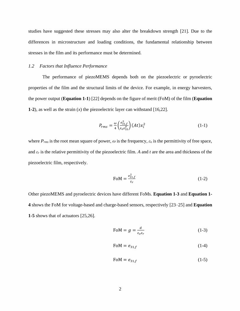
The performance of piezoMEMS depends both on the piezoelectric or pyroelectric
properties of the film and the structural limits of the device. For example, in energy harvesters,
the power output (Equation 1-1) [22] depends on the figure of merit (FoM) of the film (Equation
1-2), as well as the strain (x) the piezoelectric layer can withstand [16,22].
𝑃𝑟𝑚𝑠 =𝜔
4(
𝑒31,𝑓2
𝑜 33𝑇 ) (𝐴𝑡)𝑥𝑖
2 (1-1)
where Prms is the root mean square of power, ω is the frequency, εo is the permittivity of free space,
and εr is the relative permittivity of the piezoelectric film. A and t are the area and thickness of the
piezoelectric film, respectively.
FoM =𝑒31,𝑓
2
𝑟 (1-2)
Other piezoMEMS and pyroelectric devices have different FoMs. Equation 1-3 and Equation 1-
4 shows the FoM for voltage-based and charge-based sensors, respectively [23–25] and Equation
1-5 shows that of actuators [25,26].
FoM = 𝑔 =𝑑
𝑜 𝑟 (1-3)
FoM = 𝑒31,𝑓 (1-4)
FoM = 𝑒31,𝑓 (1-5)
3
As shown by Equations 1-1 through 1-5, each application has different requirements. This
thesis aims to understand the influences of stress on the performance of lead zirconate titanate thin
films, so that the performance of such films can be enhanced. The relationship between the total
stress in the film and its observed properties and structural limits are investigated.
1.3 Dissertation Overview
The following chapters of this thesis probe the relationship between stresses in PZT films and
the functional properties. Chapter 2 outlines the background and previous work that has been
done in the field of piezoelectrics and ferroelectrics. Additionally, Chapter 2 introduces the lead
zirconate titanate (PZT) system, with an emphasis on similarities and differences of PZT films
versus bulk ceramics. Chapter 3 discusses the effects of total stress in PZT films on the dielectric
and piezoelectric properties. These results show how stresses can tune film properties and the
importance of residual stresses on domain structure. This is further explored in Chapter 4, where
the differences in the domain structure of films with different residual stresses were investigated
from 10 K to room temperature. These results suggest differences in the energy barrier landscape
of pinning sites as a function of the residual stresses in the films.
Chapter 5 explores the mechanical limits of PZT thin films as a function of thickness and
suggests the failure strains of films are greater than that of bulk counterparts. The experimental
results were compared with a finite fracture mechanics model. Chapter 6 examines changes in the
crack initiation when films are loaded both electrically and mechanically. The electrical history is
shown to affect both the properties and the stress the film can withstand. This was attributed to the
domain structure changes with field. The results establish the limits for electromechanical failure
on PZT thin films, which is critical to exploitation of these films in piezoMEMS. These

4
relationships are summarized in Chapter 7. Chapter 7 also outlines future directions for the
studies that are presented in this thesis.
5
Chapter 2. Introduction and Background
This chapter overviews the literature that laid the foundation for the work done in this thesis.
Section 2.1 discusses the properties of piezoelectricity and electrostriction, Section 2.2 defines
pyroelectricity, Section 2.3 introduces ferroelectricity. Section 2.4 discusses the nonlinear nature
of ferroelectrics and defines intrinsic and extrinsic contributions to their properties. Section 2.4.1
and Section 2.4.2 go through the electrical techniques of Rayleigh and Preisach analysis,
respectively, to quantify the nonlinear behaviors of ferroelectrics. Section 2.5 discusses lead
zirconate titanate, the material of interest of this thesis.
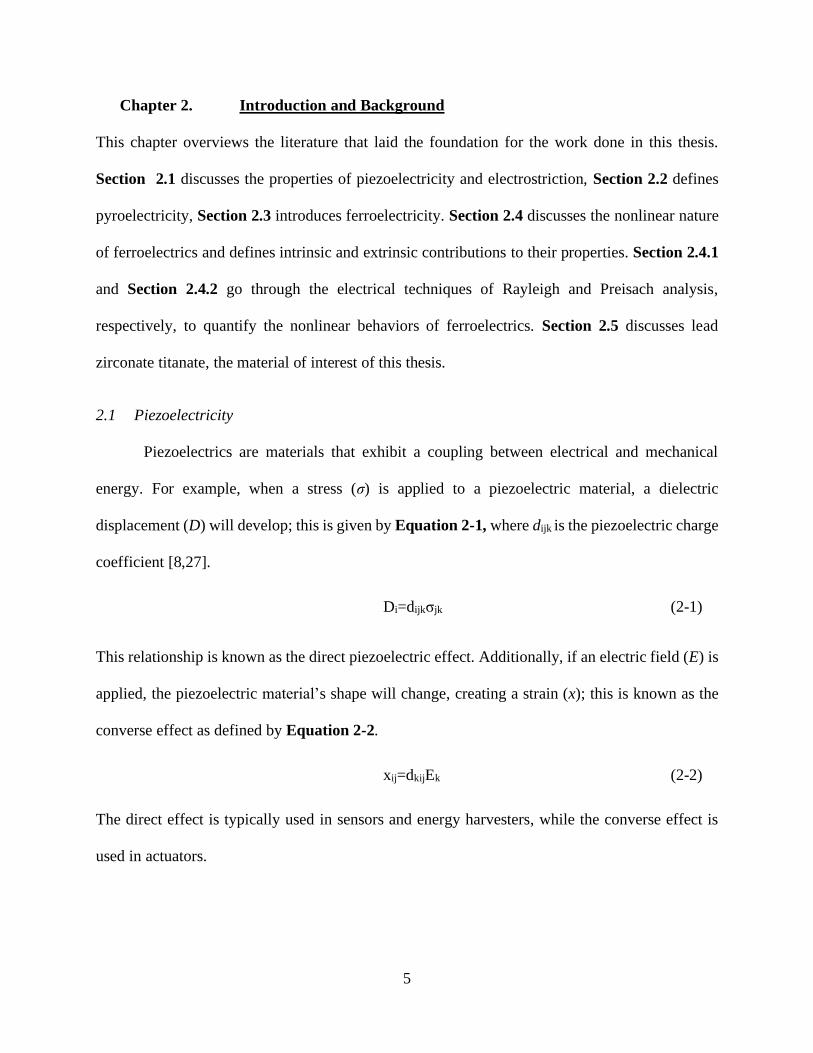
2.1 Piezoelectricity
Piezoelectrics are materials that exhibit a coupling between electrical and mechanical
energy. For example, when a stress (σ) is applied to a piezoelectric material, a dielectric
displacement (D) will develop; this is given by Equation 2-1, where dijk is the piezoelectric charge
coefficient [8,27].
Di=dijkσjk (2-1)
This relationship is known as the direct piezoelectric effect. Additionally, if an electric field (E) is
applied, the piezoelectric material’s shape will change, creating a strain (x); this is known as the
converse effect as defined by Equation 2-2.
xij=dkijEk (2-2)
The direct effect is typically used in sensors and energy harvesters, while the converse effect is
used in actuators.
6
There are a number of piezoelectric coefficients that have been defined to relate either
stress or strain to polarization or field [8,28]. The piezoelectric coefficient e is used through this
thesis and is defined by Equation 2-3.
Direct effect: Di=eiklxkl Converse effect: σij=-ekijEk (2-3)
The piezoelectric coefficients g and h are defined in Equation 2-4 and Equation 2-5, respectively.
The coefficients reported depend on the application and measurement methods used [28] .
Direct effect: 𝐸𝑖 = −𝑔𝑖𝑗𝑘 𝜎𝑗𝑘 Converse effect: 𝑥𝑖𝑗 = 𝑔𝑘𝑖𝑗𝐷𝑘 (2-4)
Direct effect: 𝐸𝑖 = −ℎ𝑖𝑗𝑘 𝑥𝑗𝑘 Converse effect 𝜎𝑗𝑘 = −ℎ𝑖𝑗𝑘 𝐷𝑖 (2-5)
Piezoelectricity is the linear response between changes in polarization and the mechanical
stress in the material. Thus, a material needs to be non-centrosymmetric to exhibit this third rank
tensor. Of the 32 crystallographic point groups, 21 groups are non-centrosymmetric [27,29,30].
However, the point group 432, while not centrosymmetric, has other symmetry elements that
prevent piezoelectricity [27,29,30]. As a result, only 20 of the point groups have this property.
While piezoelectricity is a third rank tensor, it is often reported using matrix notation. In this thesis,
e311 is reported using matrix notation as e31.
Because thin films are clamped to their substrates, it is not possible to measure the true e31
(e.g. while the in-plane strains are known, the out-of-plane strain is not known during
measurement. Instead, the out-of-plane stress is known (and is typically zero). As a result, an
effective piezoelectric coefficient e31,f which accounts for the mixed boundary conditions is
defined by Equation 2-6 [24,31].
𝑒31,𝑓 =−𝜎1
𝐸3 = 𝑒31 − 𝑒33(
𝑐13
𝑐33) (2-6)
7
Piezoelectricity can be used in many applications including timing standards, inkjet printers,
ignitors, and in piezoelectric microelectromechanical systems (piezoMEMS) such as sensors,
actuators, piezoelectric micromachined ultrasonic transducers (pMUT), and energy harvesters
[1,32].
2.2 Pyroelectricity
A subset of the piezoelectric point groups exhibits pyroelectricity. Pyroelectric materials
have a spontaneous polarization; the magnitude and/or the direction of the polarization is a
function of temperature, as defined by Equation 2-7 [8].
П𝑖 = (𝑑𝑃𝑖
𝑑𝑇) (2-7)
Of the 20 crystallographic point groups, only 10 exhibit a unique polar axis; these are referred to
as the polar point groups. Pyroelectric thin films are used in a variety of applications including
infrared imagers [3,4], thermal energy harvesters [4–7], and heat detectors [8–12].
2.3 Ferroelectricity
In certain pyroelectrics, the spontaneous polarization can be switched to other polarization
directions (defined by their crystal structure), under an applied electric field; this subclass of
pyroelectrics is known as ferroelectric materials. Some features of the crystal that favor the
observation of ferroelectricity include: d0 ions (like Ti4+), atoms with lone electron pairs (like
Pb2+), and displacements relative to a prototype phase that are small enough to allow for
reorientation but large enough to exceed the amplitude of thermal vibrations in the system [29].
Not all pyroelectrics are ferroelectric; sometimes an extremely large electric field would be
required to reorient the spontaneous polarization and this may be much greater than the electrical
breakdown strength of the material.
8
In many ways, ferroelectrics are the electrical analog to ferromagnets. At high
temperatures, most ferroelectrics undergo a phase transformation to a paraelectric phase [27]. As
a result, the system transitions from a polar ferroelectric to a non-polar paraelectric phase. The
transition temperature is known as the Curie temperature (Tc), analogous to ferromagnets. Above
this transition, the dielectric constant (εr) follows Curie-Weiss behavior, described in Equation 2-
8, where θ is the Curie-Weiss temperature [27].
휀𝑟 = 휀0 +𝐶
𝑇−𝜃 (2-8)
If the ferroelectric transition is second order, then θ is Tc. However, for a first order transition, θ
is lower than Tc [27].
When a ferroelectric is cooled below Tc, the spontaneous polarization increases and
ferroelastic strain increases. Due to the multiple possible orientations for the spontaneous
polarization and the drive to lower both the strain and depolarization energy, ferroelectrics form
regions with different spontaneous polarization directions [8]. Each region that has the same
spontaneous polarization direction (or at least nearly so) is defined as a domain. The allowed
polarization direction of the domains in the system depends on the crystal structure and the
symmetry lost on cooling through Tc.
Domain walls separate domains and are described by the angle between the polar axis
between the two domains in the system. The various domain walls are typically broken up into
two categories, 180° domain walls and non-180° domain walls. 180° domain walls are only
ferroelectrically active; an electric field must be applied for the domain wall to move. However,
non-180° domain walls are both ferroelectrically and ferroelastically active, and therefore can
move due to either an applied electric field or a mechanical force. This results in a change in
polarization and strain in the material. As a result of the various polarization orientations of each
9
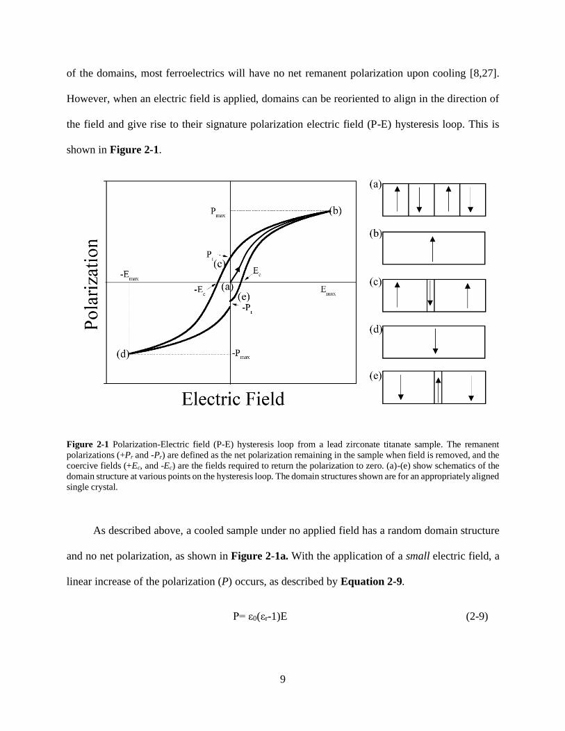
of the domains, most ferroelectrics will have no net remanent polarization upon cooling [8,27].
However, when an electric field is applied, domains can be reoriented to align in the direction of
the field and give rise to their signature polarization electric field (P-E) hysteresis loop. This is
shown in Figure 2-1.
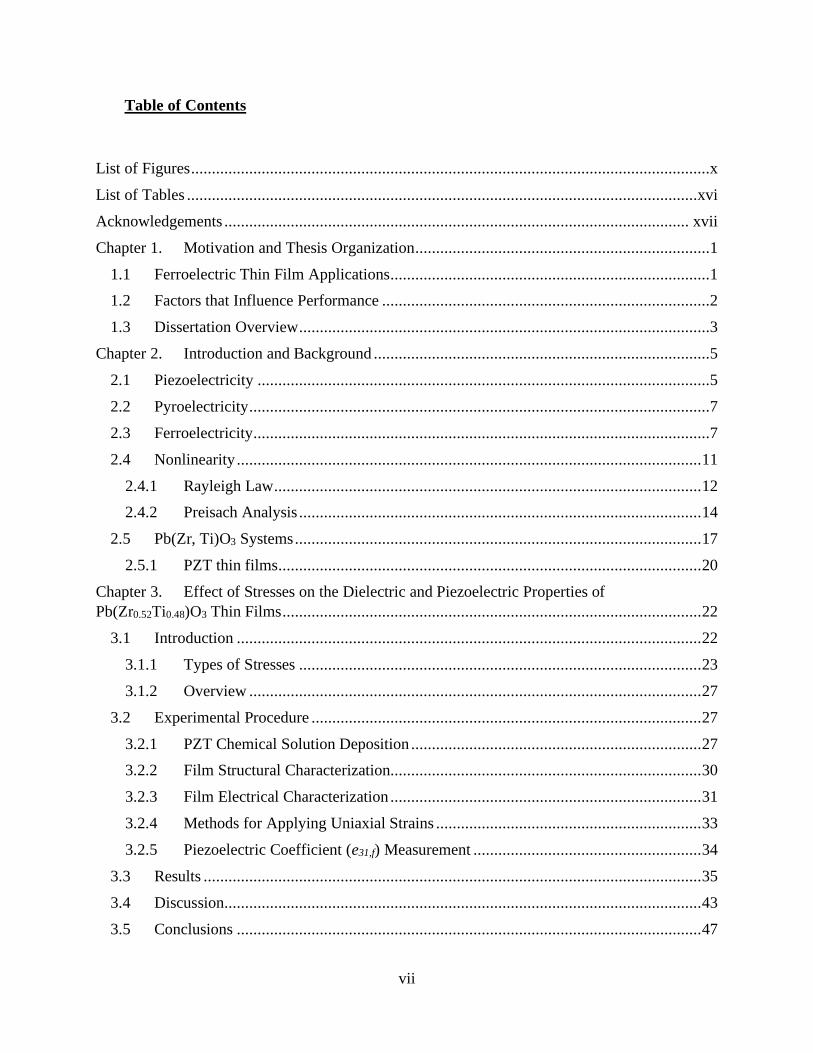
Figure 2-1 Polarization-Electric field (P-E) hysteresis loop from a lead zirconate titanate sample. The remanent
polarizations (+Pr and -Pr) are defined as the net polarization remaining in the sample when field is removed, and the
coercive fields (+Ec, and -Ec) are the fields required to return the polarization to zero. (a)-(e) show schematics of the
domain structure at various points on the hysteresis loop. The domain structures shown are for an appropriately aligned
single crystal.
As described above, a cooled sample under no applied field has a random domain structure
and no net polarization, as shown in Figure 2-1a. With the application of a small electric field, a
linear increase of the polarization (P) occurs, as described by Equation 2-9.
P= ε0(εr-1)E (2-9)
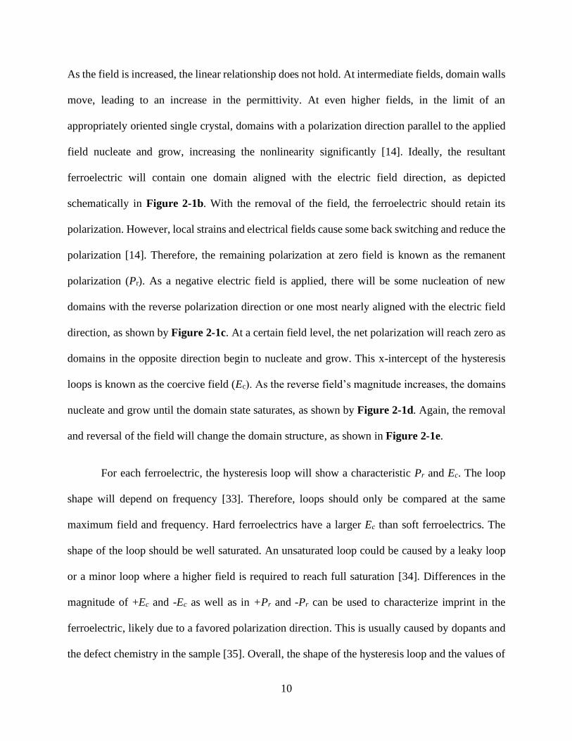
10
As the field is increased, the linear relationship does not hold. At intermediate fields, domain walls
move, leading to an increase in the permittivity. At even higher fields, in the limit of an
appropriately oriented single crystal, domains with a polarization direction parallel to the applied
field nucleate and grow, increasing the nonlinearity significantly [14]. Ideally, the resultant
ferroelectric will contain one domain aligned with the electric field direction, as depicted
schematically in Figure 2-1b. With the removal of the field, the ferroelectric should retain its
polarization. However, local strains and electrical fields cause some back switching and reduce the
polarization [14]. Therefore, the remaining polarization at zero field is known as the remanent
polarization (Pr). As a negative electric field is applied, there will be some nucleation of new
domains with the reverse polarization direction or one most nearly aligned with the electric field
direction, as shown by Figure 2-1c. At a certain field level, the net polarization will reach zero as
domains in the opposite direction begin to nucleate and grow. This x-intercept of the hysteresis
loops is known as the coercive field (Ec). As the reverse field’s magnitude increases, the domains
nucleate and grow until the domain state saturates, as shown by Figure 2-1d. Again, the removal
and reversal of the field will change the domain structure, as shown in Figure 2-1e.
For each ferroelectric, the hysteresis loop will show a characteristic Pr and Ec. The loop
shape will depend on frequency [33]. Therefore, loops should only be compared at the same
maximum field and frequency. Hard ferroelectrics have a larger Ec than soft ferroelectrics. The
shape of the loop should be well saturated. An unsaturated loop could be caused by a leaky loop
or a minor loop where a higher field is required to reach full saturation [34]. Differences in the
magnitude of +Ec and -Ec as well as in +Pr and -Pr can be used to characterize imprint in the
ferroelectric, likely due to a favored polarization direction. This is usually caused by dopants and
the defect chemistry in the sample [35]. Overall, the shape of the hysteresis loop and the values of
11
Pr and Ec are one characteristic of the quality of the ferroelectric sample. They also determine the
sample’s piezoelectric and pyroelectric responses, which are proportional to Pr.
2.4 Nonlinearity
As the hysteretic response of ferroelectric materials shows, there is an electric field
amplitude dependence of the polarization response. This is also seen in the piezoelectric and
dielectric response. Equation 2-9 is only valid at low fields for ferroelectrics, since ε depends on
the driving fields. Equation 2-10 shows the higher order terms [36].
𝑃 = 𝑃𝑜 + 𝛼1𝐸 + 𝛼2𝐸2 + 𝛼3𝐸3 + 𝛼4𝐸4 + ⋯ (2-10)
This nonlinearity is extremely important as it can increase the material’s response. To
understand these nonlinear behaviors, it is essential to distinguish between various contributions
to the dielectric and piezoelectric properties. In ferroelectric ceramics, both intrinsic and extrinsic
contributions are responsible for the primary dielectric, pyroelectric, and piezoelectric material
responses. Intrinsic contributions arise from the changes in the unit cell and the average response
of a single domain. Extrinsic contributions are due to motion of boundaries in the materials, which
includes domain wall motion and phase boundaries.
Thus, the nonlinearity can be explained by extrinsic contributions such as domain wall
motion. Domain wall motion depends on any local electric or elastic fields in the material. For
example, various defect dipoles can pin domain wall motion by creating local electric fields.
Additionally, local strains may act to pin the motion of non-180° domain walls. Certain defects
require higher energies for domain wall motion than others, creating a distribution of barrier
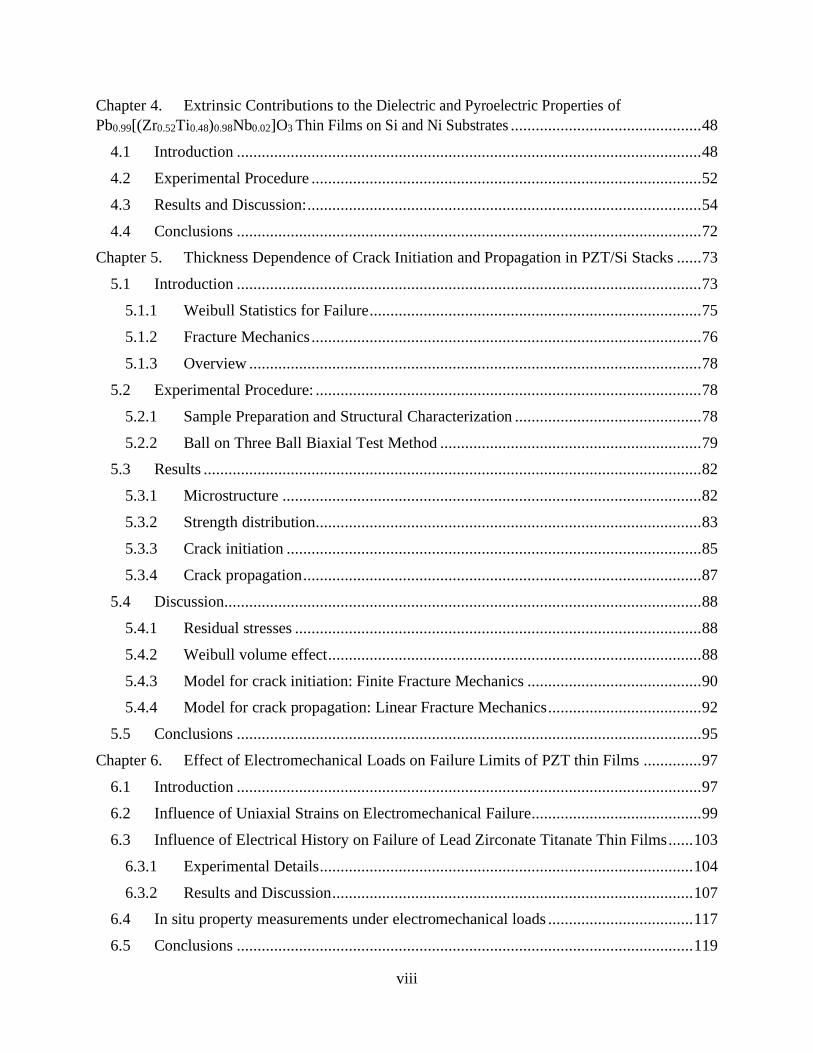
heights for domain wall motion. This is shown in Figure 2-2a. When the energy supplied by an
applied electric field is small with respect to the energy barrier, the domain wall may only displace
slightly within the potential well and will return to its original position with the removal of the
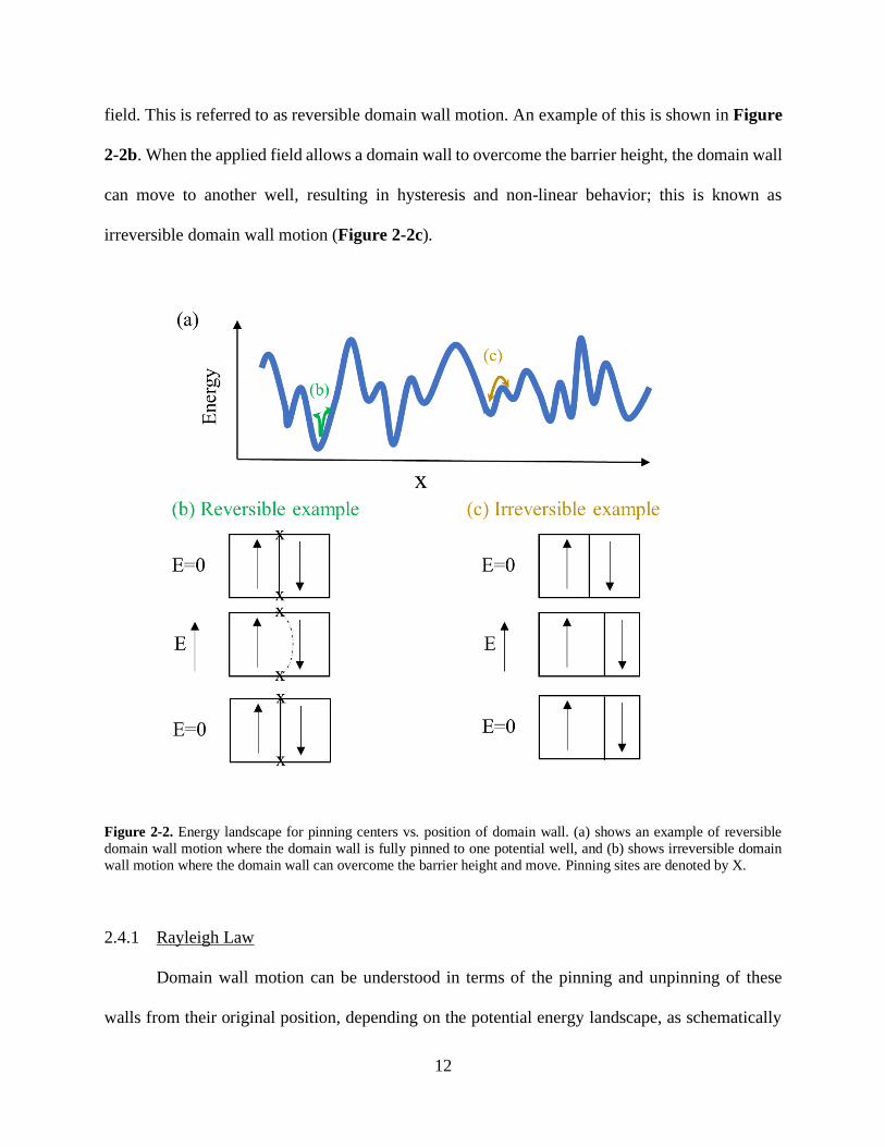
12
field. This is referred to as reversible domain wall motion. An example of this is shown in Figure
2-2b. When the applied field allows a domain wall to overcome the barrier height, the domain wall
can move to another well, resulting in hysteresis and non-linear behavior; this is known as
irreversible domain wall motion (Figure 2-2c).
Figure 2-2. Energy landscape for pinning centers vs. position of domain wall. (a) shows an example of reversible
domain wall motion where the domain wall is fully pinned to one potential well, and (b) shows irreversible domain
wall motion where the domain wall can overcome the barrier height and move. Pinning sites are denoted by X.
2.4.1 Rayleigh Law
Domain wall motion can be understood in terms of the pinning and unpinning of these
walls from their original position, depending on the potential energy landscape, as schematically
13
shown in Figure 2-2a. This has been described for both ferromagnets and ferroelectrics. For
ferromagnets, the linear dependence of the permeability on the magnetic field was first observed
by Lord Rayleigh [37] and further described by Neel [38,39], defining the Rayleigh Law. This law
states that for an intermediate field regime there is a linear change in the permeability as a function
of field amplitude, which is due to the motion of magnetic domain walls through a potential energy
landscape with a Gaussian distribution of restoring forces [40–42].
While the Rayleigh law was originally applied to magnetic permeability in ferromagnets,
it also holds true for the piezoelectric and dielectric response of many ferroelectrics [40–42]. The
Rayleigh regime is typically observed for AC electric fields with amplitudes up to roughly half of
Ec. The Rayleigh law (Equation 2-11 and Equation 2-12) shows the linear relationship between
sub-switching ac fields and the measured property [40–42]. The Rayleigh parameters εinit and dinit
describe the sum of the intrinsic and reversible domain wall motion contributions to the εr and d,
respectively. αRay describes irreversible domain wall motion contribution to the properties [40,42].
This reversible domain wall motion is favored for domain walls in deep local minima in the
potential distribution (as shown by the green arrows in Figure 2-2), and irreversible motion occurs
when the interface moves from one potential energy well to another (as shown by the brown arrow
in Figure 2-2).
휀𝑟 = 휀𝑖𝑛𝑖𝑡 + 𝛼𝑅𝑎𝑦𝐸𝑎𝑐 (2-11)
𝑑 = 𝑑𝑖𝑛𝑖𝑡 + 𝛼′𝑅𝑎𝑦𝐸𝑎𝑐 (2-12)
Various values for the Rayleigh coefficients have been reported in the literature for the
same material systems [15,40,42–44]. It has been shown that the values will depend on defect
concentrations [35,45], clamping state [43,46–48], substrate choice [44], sample thickness
[15,49,50], grain size [42,51], stresses [47,52], and composition [51].

14
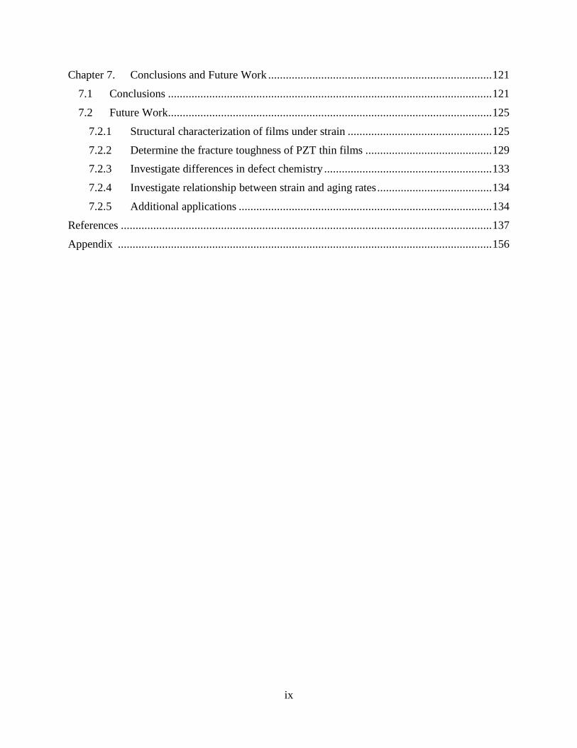
2.4.2 Preisach Analysis
Rayleigh behavior is only valid for a random Gaussian distribution of potential energy
barriers for domain wall motion, and for sub switching fields. In fact, the Rayleigh law is not valid
for all ferroelectrics, including some samples of BaTiO3 [53], and is not always valid even at all
sub-coercive fields [54]. For a more general approach, Preisach analysis and first order reversal
curves (FORC) can be used to understand the hysteresis behavior over larger field ranges, without
requiring assumptions on the potential energy landscape [55–58]. The Preisach distribution can
give valuable insight to the local coercive fields which may depend on the pinning of domains
through imprinting [35,45] and the variation in stresses [47,52] and clamping [47,48] of the films.
Figure 2-3. A schematic representation of the Preisach distribution on an α vs ß plot (otherwise known as the Preisach
plane). At four points on the plot the hysteron’s P-E loops are represented schematically. The color bar (far left)
represents the intensity at each (α, ß) point, where the red circles is the highest intensity and blue is the lowest in this
schematic example.
Preisach modeling can be used to describe switching in a ferroelectric [55–58] for an
arbitrary electrical excitation. Instead of describing nucleation and growth, this model assumes
that the ferroelectric response of a material consists of a series of rectangular hysteresis loops
defined as hysterons which are distinguished by their upwards switching field (α), and downward

15
switching field (ß) [56]. It is assumed that there are only upward and downward switching states,
and α ≥ß. Figure 2-3 shows a schematic of a Preisach distribution and the various hysterons based
on their location on the α-ß plot. When α=ß (such as (a) and (d) in Figure 2-3), the hysteron is
reversible and when α≠ß (such as (b) and (c) in Figure 2-3), the hysteron is irreversible.
The distribution of these hysterons gives rise to the polarization of the ferroelectric, as
described by Equation 2-13 [56].
P=q(α>β∫∫α,β)⋅Pirr(α,β)dαdβ+k(α)⋅Prev(α)∫dα. (2-13)
Pirr and Prev are the irreversible and reversible Preisach distributions and indicate the range of fields
required for upward and downward switching in the ferroelectric. First order reversal curves
(FORC) loops may be used to determine the Preisach distribution, as shown in Figure 2-4. When
the applied field is increased up to a given field value, all of the hysterons that have an α value less
than or equal to that field will contribute to the polarization. This is shown by the green square in
Figure 2-4b. When the field is removed, certain hysterons will switch to the opposite polarization
once the field is reduced to their ß value, as shown in the purple square ( Figure 2-4c). As the field
is increased again, as shown by the blue square ( Figure 2-4d), some hysterons will switch back.
There is some path dependence and memory in the polarization behavior of some of the hysterons;
these hysterons did not switch back when their ß field was not reached on the field down section.
As higher fields were reached, this observed memory was lost when all the hysteron aligned in the
same direction, as shown by the orange square ( Figure 2-4e).
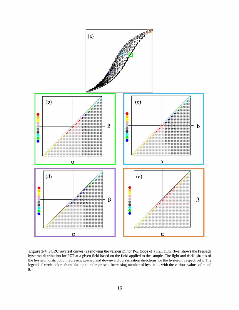
16
Figure 2-4. FORC reversal curves (a) showing the various minor P-E loops of a PZT film. (b-e) shows the Preisach
hysteron distribution for PZT at a given field based on the field applied to the sample. The light and darks shades of
the hysteron distribution represent upward and downward polzarization directions for the hysteron, respectively. The
legend of circle colors from blue up to red represent increasing number of hysterons with the various values of α and
ß.
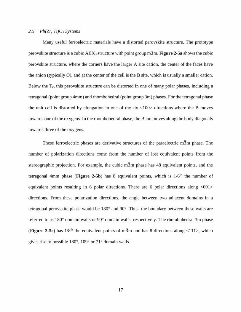
17
2.5 Pb(Zr, Ti)O3 Systems
Many useful ferroelectric materials have a distorted perovskite structure. The prototype
perovskite structure is a cubic ABX3 structure with point group m3̅m. Figure 2-5a shows the cubic
perovskite structure, where the corners have the larger A site cation, the center of the faces have
the anion (typically O), and at the center of the cell is the B site, which is usually a smaller cation.
Below the Tc, this perovskite structure can be distorted in one of many polar phases, including a
tetragonal (point group 4mm) and rhombohedral (point group 3m) phases. For the tetragonal phase
the unit cell is distorted by elongation in one of the six <100> directions where the B moves
towards one of the oxygens. In the rhombohedral phase, the B ion moves along the body diagonals
towards three of the oxygens.
These ferroelectric phases are derivative structures of the paraelectric m3̅m phase. The
number of polarization directions come from the number of lost equivalent points from the
stereographic projection. For example, the cubic m3̅m phase has 48 equivalent points, and the
tetragonal 4mm phase (Figure 2-5b) has 8 equivalent points, which is 1/6th the number of
equivalent points resulting in 6 polar directions. There are 6 polar directions along <001>
directions. From these polarization directions, the angle between two adjacent domains in a
tetragonal perovskite phase would be 180° and 90°. Thus, the boundary between these walls are
referred to as 180° domain walls or 90° domain walls, respectively. The rhombohedral 3m phase
(Figure 2-5c) has 1/8th the equivalent points of m3̅m and has 8 directions along <111>, which
gives rise to possible 180°, 109° or 71° domain walls.
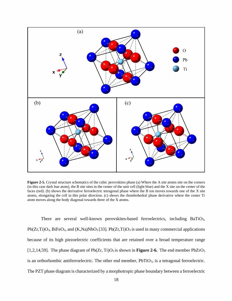
18
Figure 2-5. Crystal structure schematics of the cubic perovskites phase (a) Where the A site atoms site on the corners
(in this case dark bue atom), the B site sites in the center of the unit cell (light blue) and the X site on the center of the
faces (red). (b) shows the derivative ferroelectric tetragonal phase where the B ion moves towards one of the X site
atoms, elongating the cell in this polar direction. (c) shows the rhombohedral phase derivative where the center Ti
atom moves along the body diagonal towards three of the X atoms.
There are several well-known perovskites-based ferroelectrics, including BaTiO3,
Pb(Zr,Ti)O3, BiFeO3, and (K,Na)NbO3 [33]. Pb(Zr,Ti)O3 is used in many commercial applications
because of its high piezoelectric coefficients that are retained over a broad temperature range
[1,2,14,59]. The phase diagram of Pb(Zr, Ti)O3 is shown in Figure 2-6. The end member PbZrO3
is an orthorhombic antiferroelectric. The other end member, PbTiO3, is a tetragonal ferroelectric.
The PZT phase diagram is characterized by a morphotropic phase boundary between a ferroelectric
19
tetragonal phase and a ferroelectric rhombohedral phase. The rhombohedral phase is broken into
a high temperature rhombohedral phase with untilted oxygen octahedra (R3m) and a low
temperature phase that has tilted oxygen octahedra (R3c). At higher temperatures, the system is in
the paraelectric phase cubic phase, and Tc depends on the composition.
Figure 2-6. Phase diagram of PbZrO3-PbTiO3. C denotes the paraelectric cubic phase, O denotes Orthorhombic, R denotes rhombohedral, T denote tetragonal, M denotes monoclinic, and MPB is for the morphotropic phase boundary.
Figure is adopted from: [33,60–62]
The morphotropic phase boundary (MPB) composition of PZT is used in a variety of
applications because of its high piezoelectric response. At the MPB there are a total of 14 possible
polarization directions due to the rhombohedral (8 along the pseudo cubic <111>) and tetragonal
20
(6 along the pseudo cubic <001>) polar directions. There may be additional polarization directions
with the reported presence of a monoclinic phase at this composition as well [61–63]. It has been
reported that the MPB composition allows for easier poling, and that furthermore the
polarizabilities peak at this composition [33,64]. Because of its wide commercial interest, the
MPB composition is investigated in this study.
While the phase diagram shows the importance of the composition on the PZT system,
there are additional factors that can enhance the observed properties of PZT. The grain size and
domain size can be optimized for larger responses [65], as was shown in BaTiO3 [66].
Additionally, various dopants can alter the defect chemistry. Some donor defects such as Nb5+ and
Ta5+ on the B site can create VPb’’ [33]. These dopants act to improve domain wall motion and
create a softer ferroelectric. In contrast, acceptor dopants such as Mg2+ and Fe3+ on the B site will
create Voꞏꞏ and may create a harder ferroelectric as a result [33]. In this work, the composition and
dopant used is Pb0.99(Zr0.52Ti0.48)0.98Nb0.02O3.
2.5.1 PZT thin films
In this work, PZT films are used; these films are different from their bulk counterparts in a
number of ways [67]. First, PZT films are grown on substrates, which causes them to be under
significant amounts of residual stress [18,67–69] and are also clamped to the substrate. Clamping
limits the domain wall motion [43], in response to an external force. As a result, the measured
properties are typically suppressed when compared to bulk ceramics or released films [70–72].
Consequently, they are harder to pole. Additionally, PZT films typically have finer grain sizes and
domain sizes, which can reduce the dielectric constant, and polarization and increase the coercive
field [65,71]. Finer grains can have reduction in both extrinsic and intrinsic contributions to the
properties [65]. Additionally, scaling affects as a function of film’s thickness have been reported
21
for the dielectric, piezoelectric and ferroelectric properties of PZT thin films[71]. All of these
structural differences have been shown to contribute to suppression of properties for films [71].
To overcome some of the reduced properties, films are typically oriented through epitaxial growth
or the use of a seed layer in the substrate stack. In this thesis, the influence of residual and applied
stresses on the observed mechanical and electrical properties of PZT thin films is of particular
interest.
22
Chapter 3. Effect of Stresses on the Dielectric and Piezoelectric Properties of
Pb(Zr0.52Ti0.48)O3 Thin Films
Portions of this chapter have been reproduced from: K. Coleman, J. Walker, T. Beechem, and S.
Trolier-McKinstry, “Effect of stresses on the dielectric and piezoelectric properties of
Pb(Zr0.52Ti0.48 )O3 thin films,” J. Appl. Phys. 126 (2019) 034101. DOI:10.1063/1.5095765.
This chapter discusses the influences of stresses on the dielectric and piezoelectric properties of
PZT thin films. The total stresses in the film include residual, applied, and electrically induced
stresses. To understand the influence of residual stresses, the permittivity and P-E loops of PZT
films on Si and Ni foil were measured with varying uniaxial applied stresses. In addition, the
piezoelectric and dielectric properties were also measured as a function of applied uniaxial strain.
PZT on Ni foil was bent around a mandrel of a known radius to apply uniaxial strains. Compressive
strains of up to -0.3% and tensile strains up to 0.47% were applied. Beyond -0.3% compressive
strain, delamination was observed, and above 0.5% tensile strain, cracking was observed. PZT on
Si was strained from 0.06% compressive strain to 0.06% tensile strain using the beam bending
method, since the Si substrate is brittle. The changes in properties as a function of the total stress
suggest differences in intrinsic and extrinsic contributions between the films on Ni and Si
substrates including differences in domain structure, local stresses, and mechanical limits, which
will be explored in later chapters.
3.1 Introduction
The stress state can influence both the dielectric and piezoelectric response of ferroelectric
films [19,73,74]. Residual stresses influence the domain structure; in clamped films the remanent
and saturation polarizations depend strongly on the residual stresses as a consequence of
limitations on ferroelastic domain switching [15,18,19,68,73–77]. It is notable that applied
stresses can also strongly affect the dielectric and piezoelectric properties of piezoelectric ceramics
23
[31,59,72,78–80]. For both hard and soft PZT ceramics, applied stresses either parallel or
perpendicular to the polarization direction dramatically change the dielectric constants due to
ferroelastic domain reorientation [81–85]. Brown showed that PZT ceramics under an uniaxial
pressure of 250-300 MPa can have up to 50% reduction in the dielectric constants [81,82].
However, these stress-induced changes tend to be smaller in magnitude for thin films than bulk
ceramics exposed to the same applied stress levels [31,59,72,78,79,85,86]. This was shown in
studies by Shepard et al, where PZT films on Si have a 3-5% change in dielectric constant with
similar applied stresses [85,86].
There have been many studies on the effect of either residual stress [15,18,75,77], or
applied stresses [31,72,87] on PZT films. However, the role of a combination of residual and
applied stresses on dielectric and piezoelectric properties has not been reported over wide stress
ranges. Therefore, this study aims to quantify the effects of the total stress state on the
piezoelectric, ferroelectric, and dielectric response of PZT thin films over wide stress ranges.
3.1.1 Types of Stresses
Thin films experience stresses from various sources including residual stress (σr) associated
with the processing, applied stress induced by bending (σa), and electrically induced stress (σe) due
to piezoelectric or electrostrictive responses. The total stress (σTot) experienced by the films is the
summation of these (Equation 3-1).
σTot = σr + σe + σa (3-1)
3.1.1.1 Residual Stress
In this section, the residual stress (σr) is distinguished from the stress from thermal
expansion coefficient mismatch (σt) and the calculated residual stress from Stoney’s equation (σf).
σr in the film depends on several factors including the thickness and thermal expansion coefficients
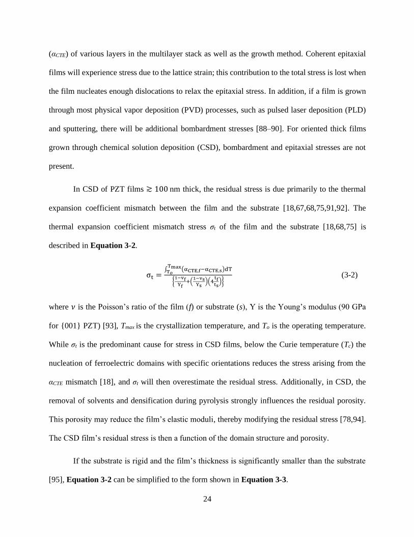
24
(αCTE) of various layers in the multilayer stack as well as the growth method. Coherent epitaxial
films will experience stress due to the lattice strain; this contribution to the total stress is lost when
the film nucleates enough dislocations to relax the epitaxial stress. In addition, if a film is grown
through most physical vapor deposition (PVD) processes, such as pulsed laser deposition (PLD)
and sputtering, there will be additional bombardment stresses [88–90]. For oriented thick films
grown through chemical solution deposition (CSD), bombardment and epitaxial stresses are not
present.
In CSD of PZT films ≳ 100 nm thick, the residual stress is due primarily to the thermal
expansion coefficient mismatch between the film and the substrate [18,67,68,75,91,92]. The
thermal expansion coefficient mismatch stress σt of the film and the substrate [18,68,75] is
described in Equation 3-2.
σt =∫ (αCTE,f−αCTE,s)dT
TmaxT𝑜
{1−vf
Yf+(
1−vsYs
)(4tfts
)} (3-2)
where 𝜈 is the Poisson’s ratio of the film (f) or substrate (s), Y is the Young’s modulus (90 GPa
for {001} PZT) [93], Tmax is the crystallization temperature, and To is the operating temperature.
While σt is the predominant cause for stress in CSD films, below the Curie temperature (Tc) the
nucleation of ferroelectric domains with specific orientations reduces the stress arising from the
αCTE mismatch [18], and σt will then overestimate the residual stress. Additionally, in CSD, the
removal of solvents and densification during pyrolysis strongly influences the residual porosity.
This porosity may reduce the film’s elastic moduli, thereby modifying the residual stress [78,94].
The CSD film’s residual stress is then a function of the domain structure and porosity.
If the substrate is rigid and the film’s thickness is significantly smaller than the substrate
[95], Equation 3-2 can be simplified to the form shown in Equation 3-3.
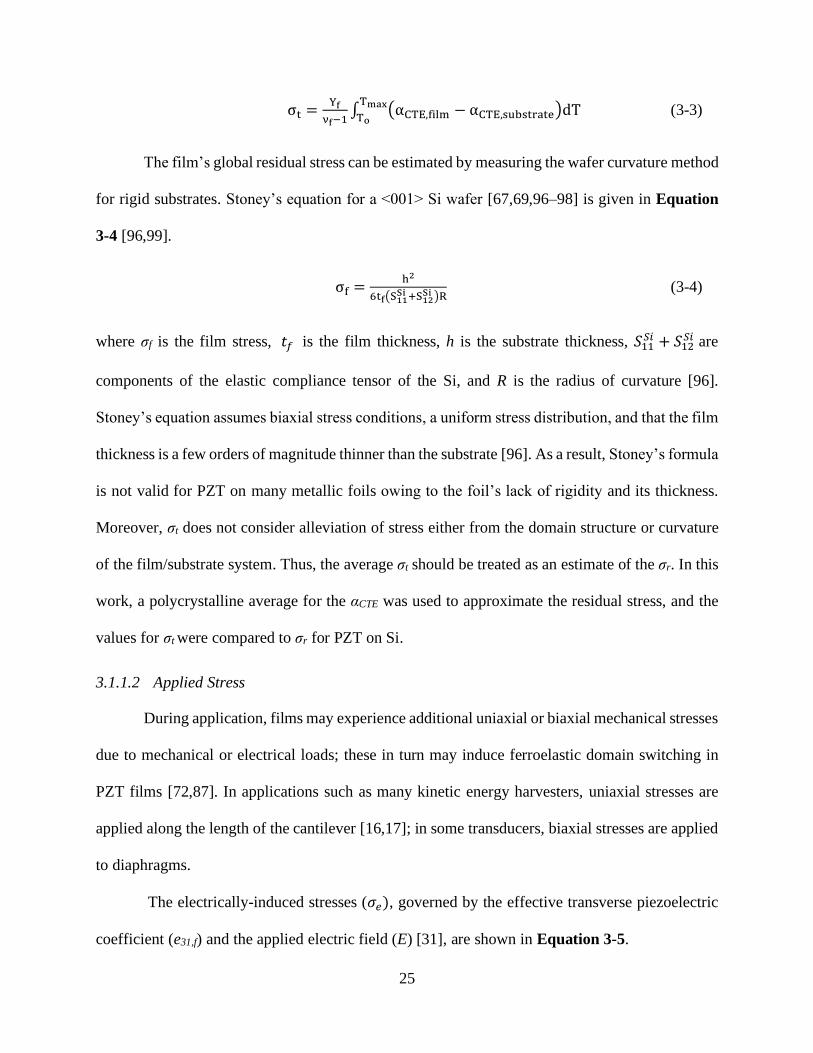
25
σt =Yf
νf−1∫ (αCTE,film − αCTE,substrate)dT
Tmax
To (3-3)
The film’s global residual stress can be estimated by measuring the wafer curvature method
for rigid substrates. Stoney’s equation for a <001> Si wafer [67,69,96–98] is given in Equation
3-4 [96,99].
σf =h2
6tf(S11Si +S12
Si )R (3-4)
where σf is the film stress, 𝑡𝑓 is the film thickness, h is the substrate thickness, 𝑆11𝑆𝑖 + 𝑆12
𝑆𝑖 are
components of the elastic compliance tensor of the Si, and R is the radius of curvature [96].
Stoney’s equation assumes biaxial stress conditions, a uniform stress distribution, and that the film
thickness is a few orders of magnitude thinner than the substrate [96]. As a result, Stoney’s formula
is not valid for PZT on many metallic foils owing to the foil’s lack of rigidity and its thickness.
Moreover, σt does not consider alleviation of stress either from the domain structure or curvature
of the film/substrate system. Thus, the average σt should be treated as an estimate of the σr. In this
work, a polycrystalline average for the αCTE was used to approximate the residual stress, and the
values for σt were compared to σr for PZT on Si.
3.1.1.2 Applied Stress
During application, films may experience additional uniaxial or biaxial mechanical stresses
due to mechanical or electrical loads; these in turn may induce ferroelastic domain switching in
PZT films [72,87]. In applications such as many kinetic energy harvesters, uniaxial stresses are
applied along the length of the cantilever [16,17]; in some transducers, biaxial stresses are applied
to diaphragms.
The electrically-induced stresses (𝜎𝑒), governed by the effective transverse piezoelectric
coefficient (e31,f) and the applied electric field (E) [31], are shown in Equation 3-5.
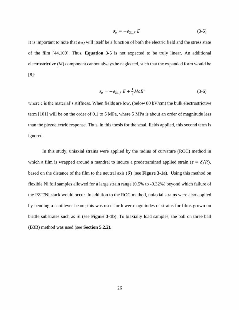
26
𝜎𝑒 = −𝑒31,𝑓 𝐸 (3-5)
It is important to note that e31,f will itself be a function of both the electric field and the stress state
of the film [44,100]. Thus, Equation 3-5 is not expected to be truly linear. An additional
electrostrictive (M) component cannot always be neglected, such that the expanded form would be
[8]:
𝜎𝑒 = −𝑒31,𝑓 𝐸 +1
2𝑀𝑐𝐸2 (3-6)
where c is the material’s stiffness. When fields are low, (below 80 kV/cm) the bulk electrostrictive
term [101] will be on the order of 0.1 to 5 MPa, where 5 MPa is about an order of magnitude less
than the piezoelectric response. Thus, in this thesis for the small fields applied, this second term is
ignored.
In this study, uniaxial strains were applied by the radius of curvature (ROC) method in
which a film is wrapped around a mandrel to induce a predetermined applied strain (휀 = 𝛿/𝑅),
based on the distance of the film to the neutral axis (𝛿) (see Figure 3-1a). Using this method on
flexible Ni foil samples allowed for a large strain range (0.5% to -0.32%) beyond which failure of
the PZT/Ni stack would occur. In addition to the ROC method, uniaxial strains were also applied
by bending a cantilever beam; this was used for lower magnitudes of strains for films grown on
brittle substrates such as Si (see Figure 3-1b). To biaxially load samples, the ball on three ball
(B3B) method was used (see Section 5.2.2).

27
Figure 3-1. Method for applying uniaxial strains on PZT films. The radius of curvature method (a) was used for higher
strains and more flexible substrates, and the beam bending method (b) was used for lower strains for the Si case.
3.1.2 Overview
{001} oriented PZT (Pb0.99⧠0.01(Zr0.52Ti0.48)0.98Nb0.02O3) films on Ni and Si substrates
were fabricated through CSD to investigate the influence of substrates with different thermal and
mechanical properties on the properties of PZT films. Electrical characterization methods were
used to explore changes in the properties and domain structure as a function of σTot. The εr and
piezoelectric coefficient, (e31,f) were measured as a function of the total stress to understand the
relationship between stress, domain state, and stress limits in piezoelectric thin films
[18,31,59,64,102].
3.2 Experimental Procedure
3.2.1 PZT Chemical Solution Deposition
PZT films were grown by chemical solution deposition (CSD) on either 50 µm thick Ni
foil or 500 µm thick Si <001> wafers. Ni foil of 99.98% purity was used from Sigma Aldrich [15].
The Ni foils were first polished using Al2O3 powders from 5 µm down to 30 nm particle size [15].
Then the NiO was removed by annealing in a reducing environment ( Po2 ~10-17 atm) at 900°C for
1 hour. Following this, a 30 nm HfO2 buffer layer was deposited by Atomic Layer Deposition
(ALD) to reduce nickel oxidation during subsequent processing steps [15,103].
28
To achieve the desired {001} orientation, a LaNiO3 (LNO) bottom electrode was deposited
by CSD using an acetic acid-based solution on both the prepared Ni foil substrates and Si wafers
with a 1 µm thermal oxide (NOVA Electronic materials). To make 120 mL of 0.2 M LNO solution,
10.397 g of lanthanum nitrate hexahydrate and 5.973 g of nickel acetate trihydrate were added to
90 mL of acetic acid and refluxed at 80°C for an hour. Then, 23 mL of acetic acid was added and
refluxed for an additional 3 hrs. The solution was cooled to room temperature and 6 mL of
deionized (DI) water was added and stirred for 30 minutes. The solution was bottled and allowed
to chelate overnight prior to use [15,104]. Then the LNO solution was spun at 3000 RPM,
pyrolyzed sequentially at 150°C and 370°C for 2 minutes each, and crystallized at 700°C for one
minute in a rapid thermal annealing furnace. This process was repeated five times to achieve a
bottom electrode of 130 nm thickness.
PZT with 2% Nb was deposited on the bottom electrode using CSD with a 0.4 Molar 2-
methoxyethanol based solution with 10% Pb excess [105]. To make 60 mL of this solution, 9.923
g of lead acetate trihydrate was added to 60 mL of 2-methoxyethanol (2MOE) and refluxed at
120°C for a minimum of 30 minutes under Ar flow. This solution was then distilled at 120°C to
remove bound water. At the same time in a glove box, the zirconium, titanium, niobium precursors
were prepared. 5.72 g of zirconium (IV) propoxide, 0.153 g of niobium (V) ethoxide, and 3.31 g
of titanium (IV) isopropoxide were added to 30 mL of 2MOE and refluxed for a half hour. Once
the Pb precursor was distilled and the Ti/Zr/Nb solution was well mixed, the two solutions were
combined with an additional 90 mL of 2MOE and refluxed for a minimum of two hours at 120°C
under Ar gas. Then the solution was distilled to 46.5 mL at 120°C to remove any remaining water.
The solution was cooled to room temperature and 13.5 mL of acetylacetone was added as a
29
stabilizer. The solution was refluxed for a minimum of 20 minutes, bottled, and left in a dry box
for 12 hours to chelate prior to use.
From this solution, films were spun at 1500 RPM, pyrolyzed at 225°C and 400°C for two
minutes each, and then crystallized at 700°C for one minute in a Pb-rich rapid thermal annealing
furnace. This process was repeated seven times to achieve a thickness of ~0.6 µm; additional
details on the deposition are provided elsewhere [15]. A PbO capping layer was added after the
7th layer to remove the pyrochlore secondary phase on the surface of the film, which formed due
to Pb volatilization during crystallization [105]. For films grown to larger thicknesses,
approximately every 5th - 7th layer, a PbO layer was utilized due to the continued volatization of
Pb during each crystallization step. When the PbO was added depended on the Pb furnace
condition and the presence of pyrochlore. To assess when the PbO layer was needed, the film
surface was checked intermittently using a field emission scanning electron microscope (FeSEM)
(see Figure 3-2); pyrochlore was manifested as very fine grained material, with higher
concentrations at the perovskite grain boundaries. If pyrochlore coated too much of the film
surface, newly deposited solution could not nucleate from the pre-existing perovskite grains, and
crystallographic orientation was progressively degraded. The PbO solution (0.08 M from lead
acetate trihydrate dissolved and distilled into 2MOE in a similar manner as the PZT solution) was
spun at 3000 RPM, pyrolyzed at 110°C for one minute, 225°C for two minutes, 410°C for two
minutes, and then crystalized at 700°C for one minute with a ramp rate of ~10°/s.

30
Figure 3-2.Various microstructures that may form depending on the lead environment of the Pb furnace and PbO
added to the film. (a) lead deficient film with a fine-grained surface pyrochlore phase which nucleated at the grain
boundaries of PZT. This film requires a PbO layer. (b) pure PZT phase, after deposition of a PbO capping layer (c)
PZT phase with a Pb-rich secondary phase on top that can be removed in acetic acid.
3.2.2 Film Structural Characterization
The orientation and phase purity of the films were characterized by a combination of X-Ray
Diffraction (XRD) using a PANalytical Empyrean diffractometer with a Cu Kα X-Ray source and
by Leo 1530 FeSEM. For XRD, first the peaks of the underlying layers were identified, as shown
in Figure 3-3. These peaks were visible due to strong orientation, the existence of low intensity
wavelengths including Cu K Beta, and so-called ghost peaks. Some peaks from nickel oxidation
and from the HfO2 buffer layer were also detected. For XRD, the following powder diffraction
files (pdf) were used: Si (00-027-1402) [106], LaNiO3 (LNO) (00-033-0710) [107], Ni (00-004-
0850) [108], NiO (00-004-0835) [109], HfO2 (00-053-0550)[110], PZT (52/48) (00-033-0784)
[111]. The numbers in parentheses correspond to the pdf file for each of the given material from
the ICDD inorganics database.

31
Figure 3-3. XRD patterns of the substrate and subsequent layers prior to the addition of the PZT layer. Peaks for the
Si and LNO for the Si substrate (a) and peaks for the Ni, HfO2 buffer and LNO for the flexible Ni substrate (b) are
labeled.
For the FeSEM, low voltages and currents were used (3.0-5.0 kV and 100 µA) since PZT
is a good insulator. For these fine grain microstructures, short working distances (2.4-3.5 mm) are
recommended. From these images, lateral grain sizes were determined using the average intercept
method with a minimum of six lines in varying directions. Unless otherwise noted, all PZT films
have a preferred {100} orientation.
3.2.3 Film Electrical Characterization
To electrically characterize these films, DC magnetron sputtered Pt top electrodes were
patterned by photolithography in diameters of 1 mm, 0.6 mm, and 0.4 mm. First, LOR 5A was
spun at 4000 RPM for 45 s and then baked at 180-190°C for two minutes. Then, SPR 3012 was
spun on at 4000 RPM for 45 s and baked at 95°C for two minutes. The photoresist was then
exposed (6.0 MJ for 7 s) and then developed in CD-26 for 70 s. The quality and sizes of the features
were checked with the optical microscope. A descum plasma etch was performed using O2 and He
gas in the M4L oxygen plasma chamber with 200 W power for two minutes prior to sputtering. Pt
was sputtered using the Kurt Lesker CMS-18 sputter tool with a power of 200 W. The Pt was
32
deposited for 417 s to achieve a thickness of 100 nm. For lift off, the sample was submerged in
acetone for a minimum of 30 minutes. This allowed the photoresist to dissolve and the Pt to lift
off the surface. Wafers were not scrubbed to prevent damage to the features. Samples were then
rinsed with DI water. To remove any remaining photoresist, samples were submerged in CD-26
and then rinsed in DI water.
The samples were then cut into cantilever beams with an aspect ratio of 1:4 or into a desired
shape. Access to the bottom electrode was made through either a wet etch or mechanical scratch.
The wet etch was performed after first painting most of the film with an 1813 photoresist protective
layer, and then baking at 120°C until hardened (typically 5 minutes). Then a drop of BOE (10:1
DI water to Hydrofluoric acid concentration) was placed on the exposed region, followed by a
drop of HCl. These steps were repeated until the bottom Pt electrode was reached. The scratch
method is performed by abrading through the PZT with a razor blade to expose the bottom
electrode and then adding silver paste to the scratched region. The silver paste was dried at room
temperature for a minimum of two hours, until the paint dried. The scratch method was the
preferred method as HCl and HF can easily etch the lanthanum nickelate bottom electrode and Ni.
The εr and the polarization-electric field (P-E) hysteresis loops were measured using a
Hewlett Packard 4284A precision LCR meter and a Radiant Multiferroic tester, respectively,
where the applied electric field was out-of-plane, perpendicular to the in-plane applied and residual
stresses. The P-E loops were measured using a single triangular wave form with no pre-pulse and
a frequency of 100 Hz.
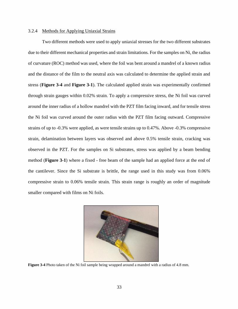
33
3.2.4 Methods for Applying Uniaxial Strains
Two different methods were used to apply uniaxial stresses for the two different substrates
due to their different mechanical properties and strain limitations. For the samples on Ni, the radius
of curvature (ROC) method was used, where the foil was bent around a mandrel of a known radius
and the distance of the film to the neutral axis was calculated to determine the applied strain and
stress (Figure 3-4 and Figure 3-1). The calculated applied strain was experimentally confirmed
through strain gauges within 0.02% strain. To apply a compressive stress, the Ni foil was curved
around the inner radius of a hollow mandrel with the PZT film facing inward, and for tensile stress
the Ni foil was curved around the outer radius with the PZT film facing outward. Compressive
strains of up to -0.3% were applied, as were tensile strains up to 0.47%. Above -0.3% compressive
strain, delamination between layers was observed and above 0.5% tensile strain, cracking was
observed in the PZT. For the samples on Si substrates, stress was applied by a beam bending
method (Figure 3-1) where a fixed - free beam of the sample had an applied force at the end of
the cantilever. Since the Si substrate is brittle, the range used in this study was from 0.06%
compressive strain to 0.06% tensile strain. This strain range is roughly an order of magnitude
smaller compared with films on Ni foils.
Figure 3-4 Photo taken of the Ni foil sample being wrapped around a mandrel with a radius of 4.8 mm.
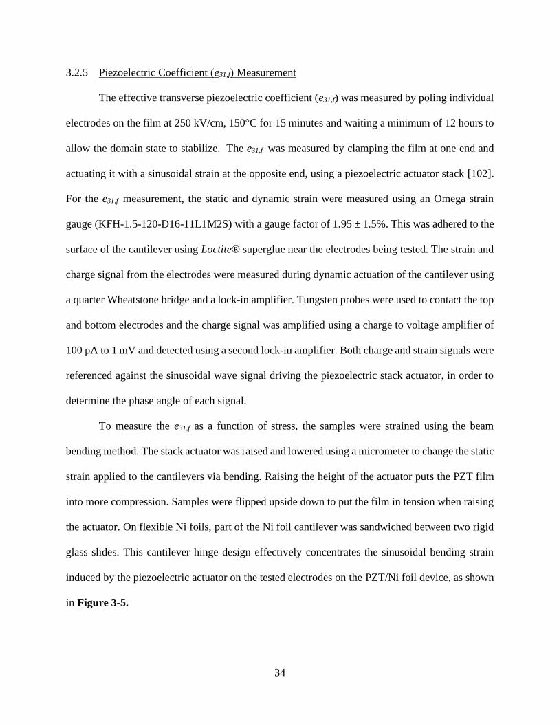
34
3.2.5 Piezoelectric Coefficient (e31,f) Measurement
The effective transverse piezoelectric coefficient (e31,f) was measured by poling individual
electrodes on the film at 250 kV/cm, 150°C for 15 minutes and waiting a minimum of 12 hours to
allow the domain state to stabilize. The e31,f was measured by clamping the film at one end and
actuating it with a sinusoidal strain at the opposite end, using a piezoelectric actuator stack [102].
For the e31,f measurement, the static and dynamic strain were measured using an Omega strain
gauge (KFH-1.5-120-D16-11L1M2S) with a gauge factor of 1.95 ± 1.5%. This was adhered to the
surface of the cantilever using Loctite® superglue near the electrodes being tested. The strain and
charge signal from the electrodes were measured during dynamic actuation of the cantilever using
a quarter Wheatstone bridge and a lock-in amplifier. Tungsten probes were used to contact the top
and bottom electrodes and the charge signal was amplified using a charge to voltage amplifier of
100 pA to 1 mV and detected using a second lock-in amplifier. Both charge and strain signals were
referenced against the sinusoidal wave signal driving the piezoelectric stack actuator, in order to
determine the phase angle of each signal.
To measure the e31,f as a function of stress, the samples were strained using the beam
bending method. The stack actuator was raised and lowered using a micrometer to change the static
strain applied to the cantilevers via bending. Raising the height of the actuator puts the PZT film
into more compression. Samples were flipped upside down to put the film in tension when raising
the actuator. On flexible Ni foils, part of the Ni foil cantilever was sandwiched between two rigid
glass slides. This cantilever hinge design effectively concentrates the sinusoidal bending strain
induced by the piezoelectric actuator on the tested electrodes on the PZT/Ni foil device, as shown
in Figure 3-5.
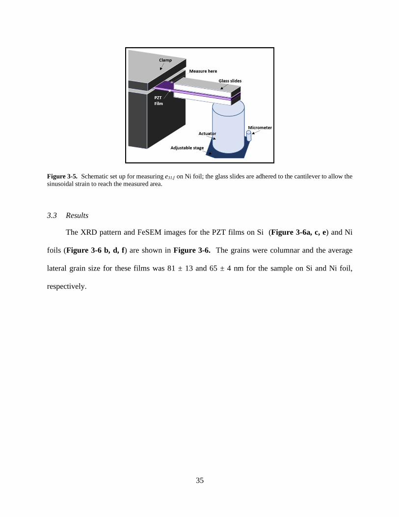
35
Figure 3-5. Schematic set up for measuring e31,f on Ni foil; the glass slides are adhered to the cantilever to allow the
sinusoidal strain to reach the measured area.
3.3 Results
The XRD pattern and FeSEM images for the PZT films on Si (Figure 3-6a, c, e) and Ni
foils (Figure 3-6 b, d, f) are shown in Figure 3-6. The grains were columnar and the average
lateral grain size for these films was 81 ± 13 and 65 ± 4 nm for the sample on Si and Ni foil,
respectively.
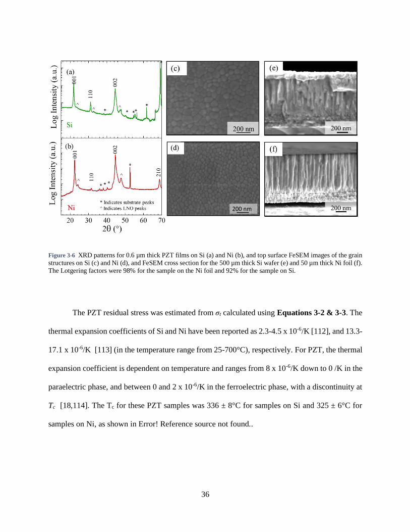
36
Figure 3-6 XRD patterns for 0.6 µm thick PZT films on Si (a) and Ni (b), and top surface FeSEM images of the grain
structures on Si (c) and Ni (d), and FeSEM cross section for the 500 µm thick Si wafer (e) and 50 µm thick Ni foil (f).
The Lotgering factors were 98% for the sample on the Ni foil and 92% for the sample on Si.
The PZT residual stress was estimated from σt calculated using Equations 3-2 & 3-3. The
thermal expansion coefficients of Si and Ni have been reported as 2.3-4.5 x 10⁻⁶/K [112], and 13.3-
17.1 x 10⁻⁶/K [113] (in the temperature range from 25-700°C), respectively. For PZT, the thermal
expansion coefficient is dependent on temperature and ranges from 8 x 10⁻⁶/K down to 0 /K in the
paraelectric phase, and between 0 and 2 x 10⁻⁶/K in the ferroelectric phase, with a discontinuity at
Tc [18,114]. The Tc for these PZT samples was 336 ± 8°C for samples on Si and 325 ± 6°C for
samples on Ni, as shown in Error! Reference source not found..

37
Figure 3-7. The relative permittivity vs temperature measured at various frequencies (from 200 Hz up to 140 kHz)
for PZT on Ni (a) and PZT on Si (b). The temperature when the derivative equals zero was assigned to be Tc for the
two films. Tc for PZT on Ni and Si were around 320°C for both films.
Using Equation 3-2, the PZT films on Ni foil were under a compressive stress of
approximately 530 ± 30 MPa, and PZT films on Si were under a tensile stress of approximately
130 ± 30 MPa. Equation 3-3 overestimates the compressive σt of the PZT on Ni since it does not
consider bowing of the substrate or the resulting domain structure. However, for PZT on Si, the
tensile σt is in agreement with σf, which was confirmed through wafer curvature measurements
(150 ± 40 MPa). Moreover, the calculated values are consistent with what has been reported in the
literature [18,19,67,69,86]. Since σf and σt do not consider the formation of domains, which will
alleviate stress, they will somewhat overestimate the magnitude of σr.
Recognizing the difference in the residual stress, Figure 3-8 compares the P-E loops of
PZT on Ni and Si at 100 Hz. At the same electrical field of 900 kV/cm, Pr was 21 ± 0.2 µC/cm2
on Si and 39.5 ± 2.3 µC/cm2 on Ni. This difference is consistent with prior reports for films under
tensile stress having more in-plane polarization and lower remanent polarizations [15,18]. It is
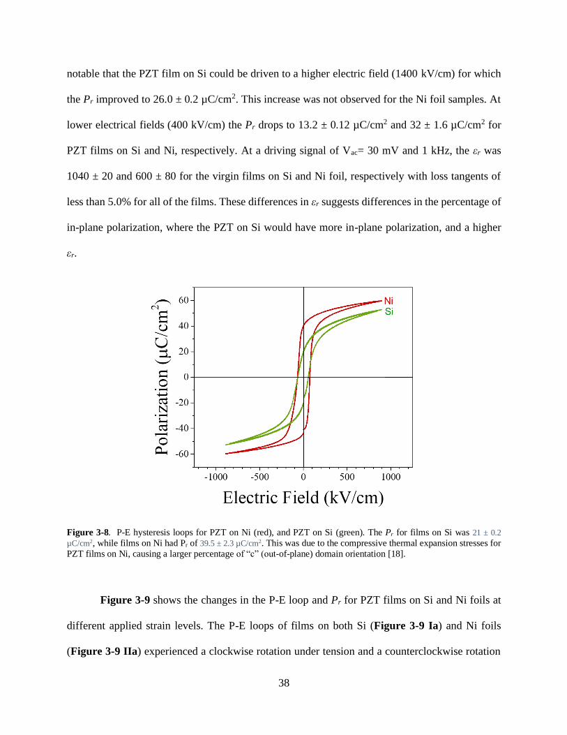
38
notable that the PZT film on Si could be driven to a higher electric field (1400 kV/cm) for which
the Pr improved to 26.0 ± 0.2 µC/cm2. This increase was not observed for the Ni foil samples. At
lower electrical fields (400 kV/cm) the Pr drops to 13.2 ± 0.12 µC/cm2 and 32 ± 1.6 µC/cm2 for
PZT films on Si and Ni, respectively. At a driving signal of Vac= 30 mV and 1 kHz, the εr was
1040 ± 20 and 600 ± 80 for the virgin films on Si and Ni foil, respectively with loss tangents of
less than 5.0% for all of the films. These differences in εr suggests differences in the percentage of
in-plane polarization, where the PZT on Si would have more in-plane polarization, and a higher
εr.
Figure 3-8. P-E hysteresis loops for PZT on Ni (red), and PZT on Si (green). The Pr for films on Si was 21 ± 0.2
µC/cm2, while films on Ni had Pr of 39.5 ± 2.3 µC/cm2. This was due to the compressive thermal expansion stresses for
PZT films on Ni, causing a larger percentage of “c” (out-of-plane) domain orientation [18].
Figure 3-9 shows the changes in the P-E loop and Pr for PZT films on Si and Ni foils at
different applied strain levels. The P-E loops of films on both Si (Figure 3-9 Ia) and Ni foils
(Figure 3-9 IIa) experienced a clockwise rotation under tension and a counterclockwise rotation
39
under compression, as has been reported previously [86]. For the films on Si, the Pr varied from
11.7 ± 0.16 µC/cm2 at 0.06% strain to 14.1 ± 0.14 µC/cm2 at -0.06% strain at 400 kV/cm. For the
films on Ni foils, Pr varied from 33 ± 1 µC/cm2 at -0.2% strain to 27.1 ± 0.7 µC/cm2 at 0.4% strain.
Upon removing the applied strains from each sample, the Pr partially recovered to the initial value
at zero applied strain. These same samples were cycled through the entire strain range again; little
hysteresis of the Pr was observed between the first and second strain cycles for films on Si (Figure
3-9 Ib). The hysteresis was more pronounced for PZT films on Ni substrates. However, it was still
<6% and a trend as a function of cycles was not distinguishable (Figure 3-9 IIb). The normalized
polarization changed approximately linearly as a function of applied strain for both films on Si
(Figure 3-9 Ic) and Ni foils (Figure 3-9 IIc). At 0.04% compressive strain the Pr increased by
roughly 5% for the PZT on Si, while on Ni a large compressive strain of 0.2% was required for
this magnitude of a change. This difference in the strain required for a 5% change in the Pr may
be due to differences in the domain structure and residual stress.
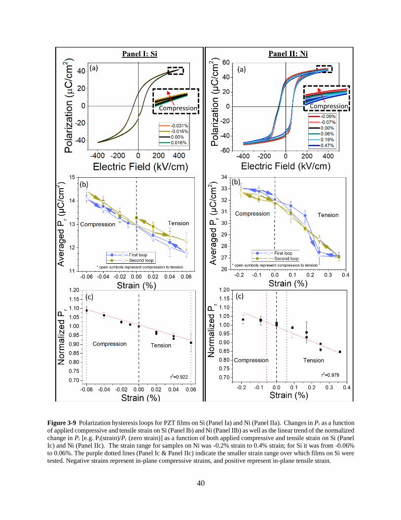
40
Figure 3-9 Polarization hysteresis loops for PZT films on Si (Panel Ia) and Ni (Panel IIa). Changes in Pr as a function
of applied compressive and tensile strain on Si (Panel Ib) and Ni (Panel IIb) as well as the linear trend of the normalized
change in Pr [e.g. Pr(strain)/Pr (zero strain)] as a function of both applied compressive and tensile strain on Si (Panel
Ic) and Ni (Panel IIc). The strain range for samples on Ni was -0.2% strain to 0.4% strain; for Si it was from -0.06%
to 0.06%. The purple dotted lines (Panel Ic & Panel IIc) indicate the smaller strain range over which films on Si were
tested. Negative strains represent in-plane compressive strains, and positive represent in-plane tensile strain.
41
To investigate how the applied strain alone influenced the domain state, dielectric Rayleigh
measurements were made at 1 kHz as a function of applied strain (Figure 3-10). The PZT on Ni
samples were strained from -0.2% to 0.5% strain, and at 1 kHz and 0 V DC bias, the AC field was
increased up to 20 kV/cm, which is less than half the coercive field. For all AC fields, the εr
increased under applied tensile strain and decreased under compressive applied strain. At an AC
driving field of 5 kV/cm (30 mV), the εr for a PZT film on Ni was 620 ± 40 at 0.5% applied tensile
strain and 460 ± 50 at 0.2% compressive strain (Figure 3-10b). The permittivity was normalized
to the value at zero applied strain and increased approximately linearly with the applied strain
(Figure 3-10b). The slope of the normalized εr change was opposite that of Pr. These changes are
consistent with changes in the domain state under high stress levels. That is, a higher “c” domain
population induced under compression should decrease the εr value, while a higher “a” domain
population in films under tensile stress is expected to increase the εr [64,115].
The permittivity in the Rayleigh regime was fitted (with an R2 of greater than 0.999) for
all strains tested and is denoted by the dashed lines in Figure 3-10a. εinit is determined from the
zero-field intercept, and αRay from the slope of the line. Both εinit and αRay increase with the applied
tensile stress. The increase in εinit may be due to an increase in reversible domain wall
contributions, a change in the intrinsic response (i.e. the percentage of “a” increases with tension),
or the combination of the two. Comparable trends in the εr as a function of applied strain were
observed for films on Si, however, the small strain range meant that the changes in permittivity
were not as pronounced. Clearer changes in properties with strain were seen for PZT on Si in
higher field measurements (i.e. P-E loops). This is consistent with previous studies of changes in
permittivity for PZT on Si substrates [86].

42
Figure 3-10 Permittivity as a function of strain and AC field for the PZT on Ni foil (a) and the normalized permittivity
as function of strain at 5 kV/cm AC field (b). Both εinit and αRay increased as a function of tensile strain. These
measurements were at 0 V DC bias.
The linear increase in the low field permittivity (Figure 3-10) and linear decrease in the Pr
(Figure 3-9) as a function of applied tensile strain suggest that tensile strain induces more in-plane
domains, which have high permittivity and lower Pr. Thus, the mechanical state likely causes
changes in the domain population of the PZT films. These effects of applied strain are also seen
on the effective transverse piezoelectric coefficient (e31,f). A lower Pr indicates that fewer domains
are aligned parallel to the electric field direction after the field has been removed; the remanent
piezoelectric response scales with Pr. Measurements at zero applied strain yielded an e31,f of –9.7
± 0.45 C/m2 for films on Ni foil and –7 ± 0.35 C/m2 for the films on Si. The difference in these
values at zero applied strain is related to the different residual stress states and domain populations
of the films. Figure 3-11 shows the changes of e31,f normalized to the zero applied strain value, as
a function of applied compressive strain for films on Si. As the compressive stress increased, the
magnitude of e31,f increased. The magnitude of this increase depends on whether the film was only
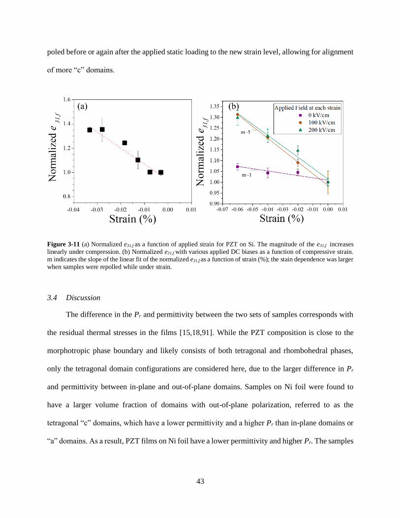
43
poled before or again after the applied static loading to the new strain level, allowing for alignment
of more “c” domains.
Figure 3-11 (a) Normalized e31,f as a function of applied strain for PZT on Si. The magnitude of the e31,f increases
linearly under compression. (b) Normalized e31,f with various applied DC biases as a function of compressive strain.
m indicates the slope of the linear fit of the normalized e31,f as a function of strain (%); the stain dependence was larger
when samples were repolled while under strain.
3.4 Discussion
The difference in the Pr and permittivity between the two sets of samples corresponds with
the residual thermal stresses in the films [15,18,91]. While the PZT composition is close to the
morphotropic phase boundary and likely consists of both tetragonal and rhombohedral phases,
only the tetragonal domain configurations are considered here, due to the larger difference in Pr
and permittivity between in-plane and out-of-plane domains. Samples on Ni foil were found to
have a larger volume fraction of domains with out-of-plane polarization, referred to as the
tetragonal “c” domains, which have a lower permittivity and a higher Pr than in-plane domains or
“a” domains. As a result, PZT films on Ni foil have a lower permittivity and higher Pr. The samples
44
on Si tend to have a lower Pr and higher permittivity because the tensile stress results in a smaller
volume fraction of “c” domains [15,18,91,116].
As seen in Figure 3-9 and Figure 3-10, an increase in the applied compressive stress also
increases the Pr and decreases the permittivity, while applied tensile stress decreases the Pr and
increases the permittivity. These changes suggest the possibility of ferroelastic domain
reorientation, as shown in the schematic in Figure 3-12. Ideally, the majority of the non-180°
domain walls could move and all domains could undergo ferroelastic switching as suggested by
row 2 of Figure 3-12. However, the permittivity and Pr on the Ni foil under the highest applied
tension did not overlap any of the values of films on Si. This suggests that many of these domains
cannot reorient. It is possible that the local strains induced from one domain switching may prevent
others from switching, as shown by row 3 of Figure 3-12 [72]. Thus, the reorientation of domains
induced by applied tensile stresses at room temperature is insufficient for the films on Ni foils to
reach a similar domain state as the samples on Si before mechanical failure ensues. Also, the
approximately linear change of both electrical properties as a function of applied strain on Ni foils
indicates that domain reorientation as a function of applied strain may be approximately constant
over the strain ranges tested. The linear trend may indicate a wide distribution in the energy
potential required for ferroelastic switching. This has been indicated by previous studies [72], but
is shown here to persist over much wider strain ranges and a larger total stress magnitude.
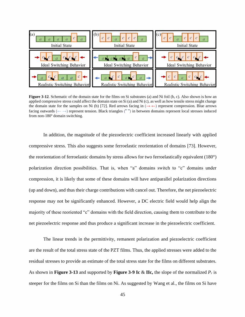
45
Figure 3-12. Schematic of the domain state for the films on Si substrates (a) and Ni foil (b, c). Also shown is how an
applied compressive stress could affect the domain state on Si (a) and Ni (c), as well as how tensile stress might change
the domain state for the samples on Ni (b) [72]. Red arrows facing in (→ ←) represent compression. Blue arrows
facing outwards (← →) represent tension. Black triangles (►◄) in between domains represent local stresses induced
from non-180º domain switching.
In addition, the magnitude of the piezoelectric coefficient increased linearly with applied
compressive stress. This also suggests some ferroelastic reorientation of domains [73]. However,
the reorientation of ferroelastic domains by stress allows for two ferroelastically equivalent (180°)
polarization direction possibilities. That is, when “a” domains switch to “c” domains under
compression, it is likely that some of these domains will have antiparallel polarization directions
(up and down), and thus their charge contributions with cancel out. Therefore, the net piezoelectric
response may not be significantly enhanced. However, a DC electric field would help align the
majority of these reoriented “c” domains with the field direction, causing them to contribute to the
net piezoelectric response and thus produce a significant increase in the piezoelectric coefficient.
The linear trends in the permittivity, remanent polarization and piezoelectric coefficient
are the result of the total stress state of the PZT films. Thus, the applied stresses were added to the
residual stresses to provide an estimate of the total stress state for the films on different substrates.
As shown in Figure 3-13 and supported by Figure 3-9 Ic & IIc, the slope of the normalized Pr is
steeper for the films on Si than the films on Ni. As suggested by Wang et al., the films on Si have
46
residual stress states closer to zero stress, which in turn is likely to result in a more complex domain
structure, with more non-180° domain walls [117]. This is also supported by estimations from
phenomenological values of the polarization and permittivity that suggest PZT on Si has roughly
60% “c” domains, resulting in a mixture of “a” and “c” [115]. Assuming a random distribution of
domains, this would suggest a high concentration of non-180° domain walls. For PZT on Ni, the
phenomenological values of permittivity and polarization suggest predominately “c” domains
(~70-85%) and so these samples would have fewer non-180° domain walls present [115].
Although the Si substrate cannot sustain wider applied strain ranges, the motion of non-180°
domain walls affects the electrical properties more significantly since “a” and “c” domains have
different properties. This may result in a larger change in the electrical properties for the films on
Si for the same applied stress. Conversely, PZT on Ni has a high percentage of “c” domains and
therefore a limited number of “a” domains that would be able to ferroelastically switch with
applied strains. This may also contribute to the smaller stress dependence of the permittivity, which
for both films on Ni and Si is much smaller than hard PZT ceramics [81–83]. Figure 3-13 also
emphasizes that while the properties of PZT can be tuned by applied stresses, due to the mechanical
limits imposed by failure, the PZT properties on one substrate do not overlap with the properties
of the film on the other substrate. In fact, these stress ranges reported for PZT films do not overlap
the stresses that maximum changes in the dielectric constants (e.g. the coercive stresses) have been
reported for PZT ceramics (~70 MPa) [83]. As a result, the initial stress state of a film after
fabrication largely determines the achievable stress range and magnitudes of electrical properties.
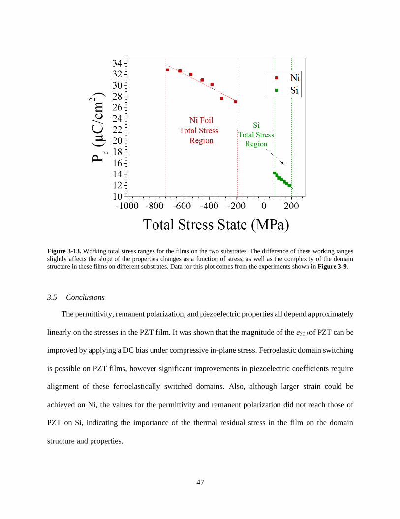
47
Figure 3-13. Working total stress ranges for the films on the two substrates. The difference of these working ranges
slightly affects the slope of the properties changes as a function of stress, as well as the complexity of the domain
structure in these films on different substrates. Data for this plot comes from the experiments shown in Figure 3-9.
3.5 Conclusions
The permittivity, remanent polarization, and piezoelectric properties all depend approximately
linearly on the stresses in the PZT film. It was shown that the magnitude of the e31,f of PZT can be
improved by applying a DC bias under compressive in-plane stress. Ferroelastic domain switching
is possible on PZT films, however significant improvements in piezoelectric coefficients require
alignment of these ferroelastically switched domains. Also, although larger strain could be
achieved on Ni, the values for the permittivity and remanent polarization did not reach those of
PZT on Si, indicating the importance of the thermal residual stress in the film on the domain
structure and properties.

48
Chapter 4. Extrinsic Contributions to the Dielectric and Pyroelectric Properties of
Pb0.99[(Zr0.52Ti0.48)0.98Nb0.02]O3 Thin Films on Si and Ni Substrates
Portions of this chapter come from: K. Coleman1*, S. Shetty1, B Hanrahan2, W. Zhu1, and S. Trolier-
McKinstry1 “Extrinsic contributions to the dielectric and pyroelectric properties of
Pb0.99[(Zr0.52Ti0.48)0.98Nb0.02]O3 thin films on Si and Ni substrates” accepted 2020
This chapter investigates the differences in the extrinsic contributions to the dielectric and
pyroelectric properties of Pb0.99[(Zr0.52Ti0.48)0.98Nb0.02]O3 (PZT) films on Ni foil and Si wafers by
using Rayleigh analysis, third harmonic phase angle, and Preisach analysis from 15 K to 296 K.
The temperature dependence of the domain structure, domain wall mobility, and domain switching
influenced the intrinsic, extrinsic, and secondary contributions to the pyroelectric coefficients.
This, in turn, produced markedly different room temperature pyroelectric coefficients of ~250
µC/m2K and ~100 µC/m2K, respectively, for films on Ni and Si. At room temperature, the
dielectric irreversible Rayleigh parameter αray was 15.5 ± 0.1 and 28.4 ± 1.6 cm/kV for PZT on Si
and Ni, respectively. The higher αray value for the Ni sample suggests more domain wall motion
at room temperature, which was attributed to the lower stiffness on the Ni foil compared to the
~500 µm thick Si substrate. Below 200 K, αray for the PZT Si sample exceeds that of the Ni/PZT
sample. This is believed to arise from differences in the energy landscape of pinning centers for
domain wall motion. It is proposed that the residual stresses not only set the preferred domain
structures, but also the barrier heights for domain wall motion and domain switching.
4.1 Introduction
Pyroelectric thin films are used in infrared imagers [3,4,118–121], thermal energy
harvesters [4,7,122–124], and detectors of thermal infra-red radiation [8–10,119,125–128] The
performance of these devices depends on the pyroelectric coefficient, , of the film, which is
determined by the change in polarization with temperature [8]. At zero applied field, which is the
49
condition for this chapter, the change in polarization with temperature depends on several factors,
as shown in Equation 4-1 [6,129].
П𝑡𝑜𝑡𝑎𝑙 = (𝜕𝐷
𝜕𝑇)
𝑥+ (
𝜕𝐷
𝜕𝑋)
𝑇(
𝜕𝑋
𝜕𝑥)
𝑡(
𝜕𝑥
𝜕𝑇)
𝑋+ 𝑃𝑠 (
𝜕𝜑𝐶
𝜕𝑇) (4-1)
The primary pyroelectric response is due to the change in the magnitude of the spontaneous
polarization with temperature. There is also a secondary term due to a stress induced response due
to the piezoelectric response of the film, which induces a polarization due to the change in
dimensions associated with a temperature change [6,124,130]. Lastly, there also can be an
extrinsic contribution from motion of domain walls or phase boundaries[131]. In the case where
heating is not uniform, an additional term is also possible [129], but this is typically negligible for
thin films clamped to substrates with good thermal conductivity (such as Si and metallic substrates)
[6], and so it is not included in Equation 1. The combination of the secondary and extrinsic
contributions can account for up to a third of the pyroelectric coefficient [132] with tuning of strain
in the film. Studies show that changing the epitaxial stain and the thermal expansion mismatch
between the film and substrate can increase the pyroelectric coefficient significantly
[122,124,132,133].
It is important to recognize, however, that thermal stresses will also modulate other
contributions to the net pyroelectric effect. In particular, the thermal expansion mismatch stress
between the film and the substrate influences the percentage of out-of-plane “c” and in-plane “a”
domains in {001} oriented perovskite films with a significant tetragonal phase fraction [18,19,75].
This changes the intrinsic pyroelectric coefficient. Additionally, changes in temperature and stress
also influence the domain populations and types of domain walls present in the films, and hence
the extrinsic contributions to pyroelectricity [44,117,124,132]. Finally, local stresses in the film
50
may pin certain types of domain walls, [72] and determine the domain wall density [117] and
domain structure [132].
In PZT films, the extrinsic contribution to the pyroelectric coefficient is hard to predict due
to the complex domain structure and various degrees of clamping. For example, a substrate’s
stiffness and thickness influence the degree of in-plane clamping experienced by the film
[15,20,77] and thereby alter the extrinsic contributions to properties. Changes in the film’s stress
state can significantly alter the amount of domain wall motion; this has been demonstrated by
reduction of stress through releasing the films from the underlying substrate [20,43,134], as well
as by varying epitaxial strains [132]. However, to date, the relationship between stresses and
domain wall pinning sites is not fully understood. This complicates prediction of the functional
pyroelectric, dielectric, and piezoelectric responses of ferroelectric thin films, and reduces the
accuracy of calculations on the high field response of sensors and actuators.
For example, stresses may affect the extent of domain wall motion at low fields, and
domain nucleation and growth at higher fields. Therefore, the influence of stresses should be
explored using both low and high field methods. At lower fields, the dielectric non-linearities of
many ferroelectrics can be described through the Rayleigh law (Section2.4.1) [40,42], as in
Equation 4-2.
휀𝑟 = 휀𝑖𝑛𝑖𝑡 + 𝛼𝑅𝑎𝑦𝐸𝑎𝑐 (4-2)
where εinit captures the response due to reversible domain wall motion and intrinsic contributions
and αRay quantifies the irreversible domain wall motion (αRay) to the permittivity. Analysis of the
Rayleigh response for films on various substrates [15,44] suggests that films with flexible
substrates exhibit higher domain wall contributions to the properties than more fully clamped films
on rigid substrates. Because domain wall motion is thermally activated, temperature dependent
51
Rayleigh measurements can provide one means of semi-quantifying the depth of the potential wells
pinning domain walls, since at low temperatures, mobile interfaces can be frozen out of the
response [36].
To confirm Rayleigh behavior at lower temperatures, the phase angles (δi) of the higher
harmonics of the dielectric response can be used to determine the Rayleigh regime [36,54]. In
particular, δ3 should be at -90° (note a change in sign convention between references [135,136]
and reference [54]). It has been shown that the phase angle may require a threshold field to reach
the Rayleigh regime at some temperatures, which can give insight into the energy barrier ranges
for domain wall motion.
Additionally, Preisach distributions (or more generally first order reversal curve (FORC)
distributions) [55,57,58] describe the switching distributions over a much wider range of fields
than is captured by Rayleigh behavior [58]. These models describe switching in terms of a
distribution of hysterons, where each hysteron has a characteristic positive switching field (α) and
negative switching field (ß) [58]. It is assumed that α is greater than ß. See Section 2.4.2 for more
detail. While this model does not illuminate the detailed mechanisms for switching, it does allow
the temperature dependence of the switching distributions to be described. This is useful as the
local coercive fields depends on the pinning of domains through imprinting [35,45] and the
variation in stresses [47,52] and clamping [47,48] of the films. Since the FORC distribution covers
a higher field range, it may suggest some differences in pinning centers which may lead to different
ideal poling conditions of films under different stress states. Determining these differences in
energy barrier height for low field and high field conditions is necessary to fully quantify and
exploit the extrinsic response of the film to optimize various properties.
52
In this chapter, the link between extrinsic contributions to the dielectric and pyroelectric
properties based on stresses in 0.6 µm thick Pb0.99□0.01[(Zr0.52Ti0.48)0.98Nb0.02]O3 (PZT) films on Ni
and Si substrates was explored. PZT was used since it has good piezoelectric and pyroelectric
coefficients and is used in many commercial applications [1,2]. Rayleigh and Preisach analysis as
well as δ3 values were used to compared domain wall motion at low fields and switching behavior
at high fields from 10 K up to room temperature (296 K). From these results, working models of
the potential energy landscapes and domain structure were developed to convey the differences in
extrinsic contributions from one PZT thin film to another, based on residual stresses.
4.2 Experimental Procedure
The 0.6 µm PZT films used in this study were the same series of films grown in Chapter
3. Details of the chemical solution deposition (CSD) process using a 2-methoxyethanol based
solution [15,44,105] are described in Section 3.2.1. The X-Ray diffraction patterns and FeSEM
images of these films are shown in Figure 3-6.
The pyroelectric coefficient of PZT on Ni and Si were measured by heating the substrates
using a cartridge heater powered by a 50% duty cycle square wave while monitoring the
temperature and sample current. Equation 4-3 relates the pyroelectric coefficient, П, to
heating/cooling and sample properties
П =𝐼П
𝐴𝑑𝑇𝑑𝑡⁄
(4-3)
where 𝐴 is the current collection area, 𝐼𝛱 is the pyroelectric current, T is temperature and t is time.
For the temperature measurement, a co-located, surrogate thin film platinum resistive thermal
device (RTD) was used estimate the pyroelectric thin film temperature. The thermal properties of
the Ni and Si substrates were modeled to ensure the accuracy of the surrogate RTD chip [133].
Additional electrical characterization of the films was performed using a Lakeshore Cryotronics
53
8400 series temperature-controlled probe station from 10 K to 296 K. Samples were adhered to
the stage using a thin layer of GE Varnish to ensure good thermal contact. A Cernox thin film RTD
cryogenic temperature sensor on a glass substrate was adhered on the stage using a thin layer of
GE varnish near the samples to monitor the temperature. Measurements as a function of
temperature were made on heating from 10 K.
First, P-E hysteresis loops were measured using a custom built electric field loop system
using a AC voltage amplifier (790 series power amplifier Piezotronics Inc.) described elsewhere
[45,137]. One set of loops was measured up to 400 kV/cm at 100 Hz and the coercive field (Ec)
and remanent polarization (Pr) were recorded. Since the Ec drastically increases with decreasing
temperature, polarization hysteresis loops were repeated at 4x Ec to obtain fully saturated loops.
Low field measurements of permittivity of PZT on Ni and Si were acquired using a Hewlett
Packard LCR meter at 1 kHz and 30 mV AC signal [136]. The first, second, and third harmonics
of the permittivity and their respective phase angles at 1 kHz were determined using a lock-in
amplifier as an AC voltage source, which was swept up to half the coercive field at each
temperature. Rayleigh measurements of the permittivity were taken at 1 kHz using the LCR meter
and an AC signal up to 25 kV/cm. The Rayleigh parameters were determined by a linear best fit in
the Rayleigh regime [43].
To probe the dielectric response at higher fields, FORC were measured using 40 loops that
increased linearly in field up to 4 times the coercive field, as described elsewhere [45,137]. The
field range probed was from -4Ec to +4Ec at each temperature. The Preisach distribution was
determined from these loops, as described elsewhere [45,137].
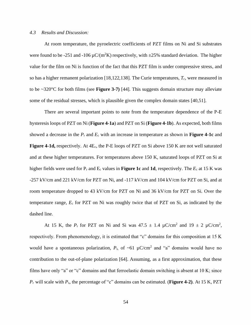
54
4.3 Results and Discussion:
At room temperature, the pyroelectric coefficients of PZT films on Ni and Si substrates
were found to be -251 and -106 µC/(m2K) respectively, with ±25% standard deviation. The higher
value for the film on Ni is function of the fact that this PZT film is under compressive stress, and
so has a higher remanent polarization [18,122,138]. The Curie temperatures, Tc, were measured in
to be ~320°C for both films (see Figure 3-7) [44]. This suggests domain structure may alleviate
some of the residual stresses, which is plausible given the complex domain states [40,51].
There are several important points to note from the temperature dependence of the P-E
hysteresis loops of PZT on Ni (Figure 4-1a) and PZT on Si (Figure 4-1b). As expected, both films
showed a decrease in the Pr and Ec with an increase in temperature as shown in Figure 4-1c and
Figure 4-1d, respectively. At 4Ec, the P-E loops of PZT on Si above 150 K are not well saturated
and at these higher temperatures. For temperatures above 150 K, saturated loops of PZT on Si at
higher fields were used for Pr and Ec values in Figure 1c and 1d, respectively. The Ec at 15 K was
-257 kV/cm and 221 kV/cm for PZT on Ni, and -117 kV/cm and 104 kV/cm for PZT on Si, and at
room temperature dropped to 43 kV/cm for PZT on Ni and 36 kV/cm for PZT on Si. Over the
temperature range, Ec for PZT on Ni was roughly twice that of PZT on Si, as indicated by the
dashed line.
At 15 K, the Pr for PZT on Ni and Si was 47.5 ± 1.4 µC/cm2 and 19 ± 2 µC/cm2,
respectively. From phenomenology, it is estimated that “c” domains for this composition at 15 K
would have a spontaneous polarization, Ps, of ~61 µC/cm2 and “a” domains would have no
contribution to the out-of-plane polarization [64]. Assuming, as a first approximation, that these
films have only “a” or “c” domains and that ferroelastic domain switching is absent at 10 K; since
Pr will scale with Ps, the percentage of “c” domains can be estimated. (Figure 4-2). At 15 K, PZT
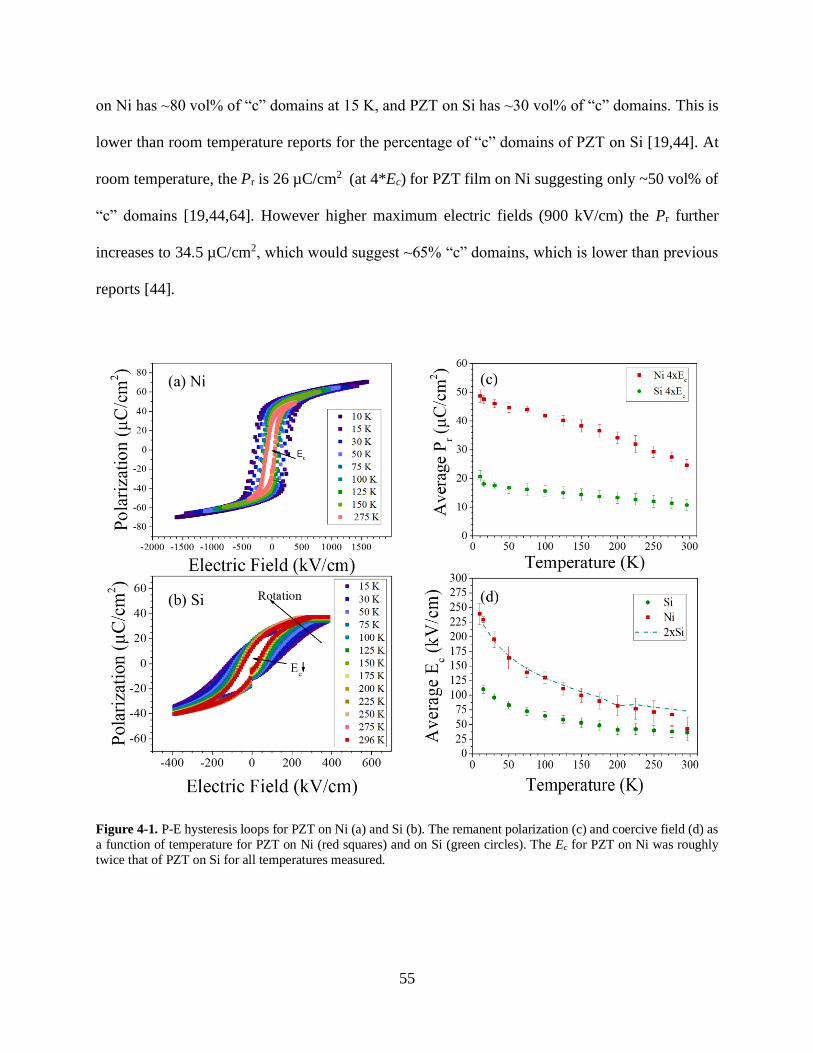
55
on Ni has ~80 vol% of “c” domains at 15 K, and PZT on Si has ~30 vol% of “c” domains. This is
lower than room temperature reports for the percentage of “c” domains of PZT on Si [19,44]. At
room temperature, the Pr is 26 µC/cm2 (at 4*Ec) for PZT film on Ni suggesting only ~50 vol% of
“c” domains [19,44,64]. However higher maximum electric fields (900 kV/cm) the Pr further
increases to 34.5 µC/cm2, which would suggest ~65% “c” domains, which is lower than previous
reports [44].
Figure 4-1. P-E hysteresis loops for PZT on Ni (a) and Si (b). The remanent polarization (c) and coercive field (d) as
a function of temperature for PZT on Ni (red squares) and on Si (green circles). The Ec for PZT on Ni was roughly
twice that of PZT on Si for all temperatures measured.
56
Figure 4-2. Estimated Pr values from phenomenology at 15 K (blue) and 296 K (pink) based on the percentage of “c”
domains (a), and the observed Pr for PZT samples on Ni and Si.
The difference in the volume fraction of “c” domains at 15 K and room temperature can be
attributed to extrinsic contributions to the property changes or to domain reorientation with
changes in stress with temperature, or a combination of these. The stress changes in the film due
to thermal expansion mismatch stress (σt) is defined by Equation 4-4. 𝛼𝐶𝑇𝐸 is the coefficient of
thermal expansion, v is the Poisson’s ratio, Y is the Young’s modulus and t is the thickness for the
film (f) and substrate (s).
𝜎𝑡 =∫ (𝛼𝐶𝑇𝐸,𝑓−𝛼𝐶𝑇𝐸,𝑠)𝑑𝑇
𝑇𝑚𝑎𝑥𝑇𝑐
{1−𝑣𝑓
𝑌𝑓+(
1−𝑣𝑠𝑌𝑠
)(4𝑡𝑓
𝑡𝑠)}
(4-4)
For the temperature range used here (15 K to 296 K) the αCTE for Ni varies from 0.02 to
13.3 ppm/K [113,139] and Si from -0.5 to 2.6 ppm/K [112,140]. The αCTE for PZT below 273 K
has not been reported, but in the ferroelectric regime αCTE has been reported to be roughly 2 ppm/K
[18,114,141]. The volumetric thermal expansion coefficient was estimated from the results in
[142–144] and below 60 K it is assumed that the αCTE for PZT decreases linearly to 0 ppm/K as 0
K is approached for the calculation. Therefore, approximately -200 MPa and -5 MPa more stress
is added to PZT on Ni and Si, respectively, when it is cooled from room temperature down to 15
57
K. The small change in stress for the sample on Si produces little ferroelastic switching, such that
the volume fraction of “c” domains is approximately constant at cryogenic temperatures. As shown
in Figure 3-13, the Pr of PZT films on Ni would increase by 2.5 µC/cm2 under -200 MPa [44],
which suggests an increase in “c” domains as the temperature is reduced [64], but additional
contributions must be considered since there are limitations to these phenomenological
assumptions [51].
Rayleigh behavior and higher harmonics of the dielectric constant were investigated down
to 10 K to determine the extent of domain wall motion at lower temperatures. At the onset of the
Rayleigh regime, the phase angle of the third harmonic switches from -180° to -90° as domain
walls begin to contribute to the permittivity [54] (note that the sign of the phase angle has been
changed to be consistent with recent reports [135]). The first, second, and third harmonics are
reported in Appendix. For perfect Rayleigh behavior in an unpoled sample, only the odd
harmonics should be present [145]. However, small values for the second harmonic were seen and
attributed to slight poling of the samples with the applied field, which is consistent with previous
studies on PZT films [145].
Figure 4-3 shows that the third harmonic phase angle for PZT on Ni and Si shifts
from -180° to -90° on increasing magnitude of the electric field. Consistent with previous reports
[54], there is a threshold field required to reach -90°, suggesting that the entire energy landscape
distribution for domain wall motion is greater than 0 eV. As the temperature decreases, the AC
field required to reach the Rayleigh-like regime rises. The field where the third harmonic phase
angle first reaches -90 ± 5° is denoted as Eδ3. It is notable that there is a larger deviation from the
90° phase angle for films on Si, relative to films on Ni. The results were reproducible, but the
origin of this behavior is not known, but may indicate an additional conduction mechanism. This
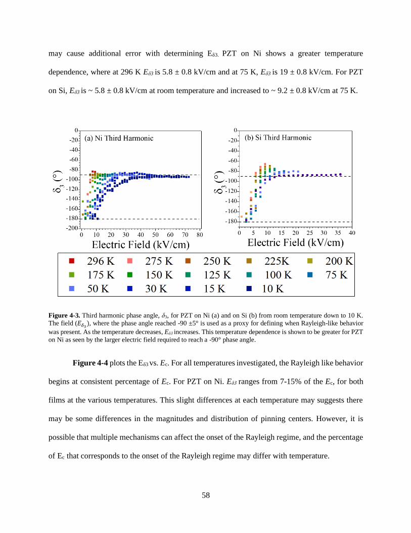
58
may cause additional error with determining Eδ3. PZT on Ni shows a greater temperature
dependence, where at 296 K Eδ3 is 5.8 ± 0.8 kV/cm and at 75 K, Eδ3 is 19 ± 0.8 kV/cm. For PZT
on Si, Eδ3 is ~ 5.8 ± 0.8 kV/cm at room temperature and increased to ~ 9.2 ± 0.8 kV/cm at 75 K.
Figure 4-3. Third harmonic phase angle, δ3, for PZT on Ni (a) and on Si (b) from room temperature down to 10 K.
The field (𝐸𝛿3), where the phase angle reached -90 ±5° is used as a proxy for defining when Rayleigh-like behavior
was present. As the temperature decreases, Eδ3 increases. This temperature dependence is shown to be greater for PZT
on Ni as seen by the larger electric field required to reach a -90° phase angle.
Figure 4-4 plots the Eδ3 vs. Ec. For all temperatures investigated, the Rayleigh like behavior
begins at consistent percentage of Ec. For PZT on Ni. Eδ3 ranges from 7-15% of the Ec, for both
films at the various temperatures. This slight differences at each temperature may suggests there
may be some differences in the magnitudes and distribution of pinning centers. However, it is
possible that multiple mechanisms can affect the onset of the Rayleigh regime, and the percentage
of Ec that corresponds to the onset of the Rayleigh regime may differ with temperature.
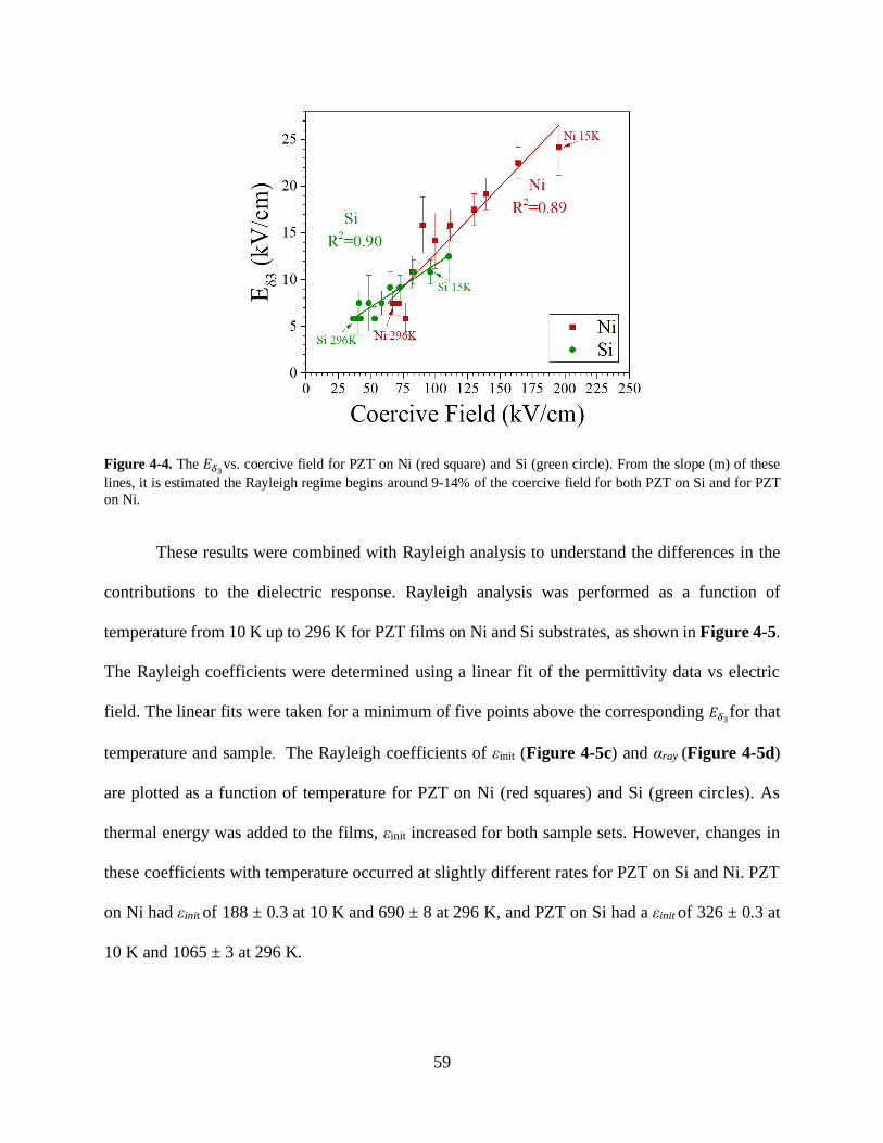
59
Figure 4-4. The 𝐸𝛿3vs. coercive field for PZT on Ni (red square) and Si (green circle). From the slope (m) of these
lines, it is estimated the Rayleigh regime begins around 9-14% of the coercive field for both PZT on Si and for PZT
on Ni.
These results were combined with Rayleigh analysis to understand the differences in the
contributions to the dielectric response. Rayleigh analysis was performed as a function of
temperature from 10 K up to 296 K for PZT films on Ni and Si substrates, as shown in Figure 4-5.
The Rayleigh coefficients were determined using a linear fit of the permittivity data vs electric
field. The linear fits were taken for a minimum of five points above the corresponding 𝐸𝛿3for that
temperature and sample. The Rayleigh coefficients of εinit (Figure 4-5c) and αray (Figure 4-5d)
are plotted as a function of temperature for PZT on Ni (red squares) and Si (green circles). As
thermal energy was added to the films, εinit increased for both sample sets. However, changes in
these coefficients with temperature occurred at slightly different rates for PZT on Si and Ni. PZT
on Ni had εinit of 188 ± 0.3 at 10 K and 690 ± 8 at 296 K, and PZT on Si had a εinit of 326 ± 0.3 at
10 K and 1065 ± 3 at 296 K.
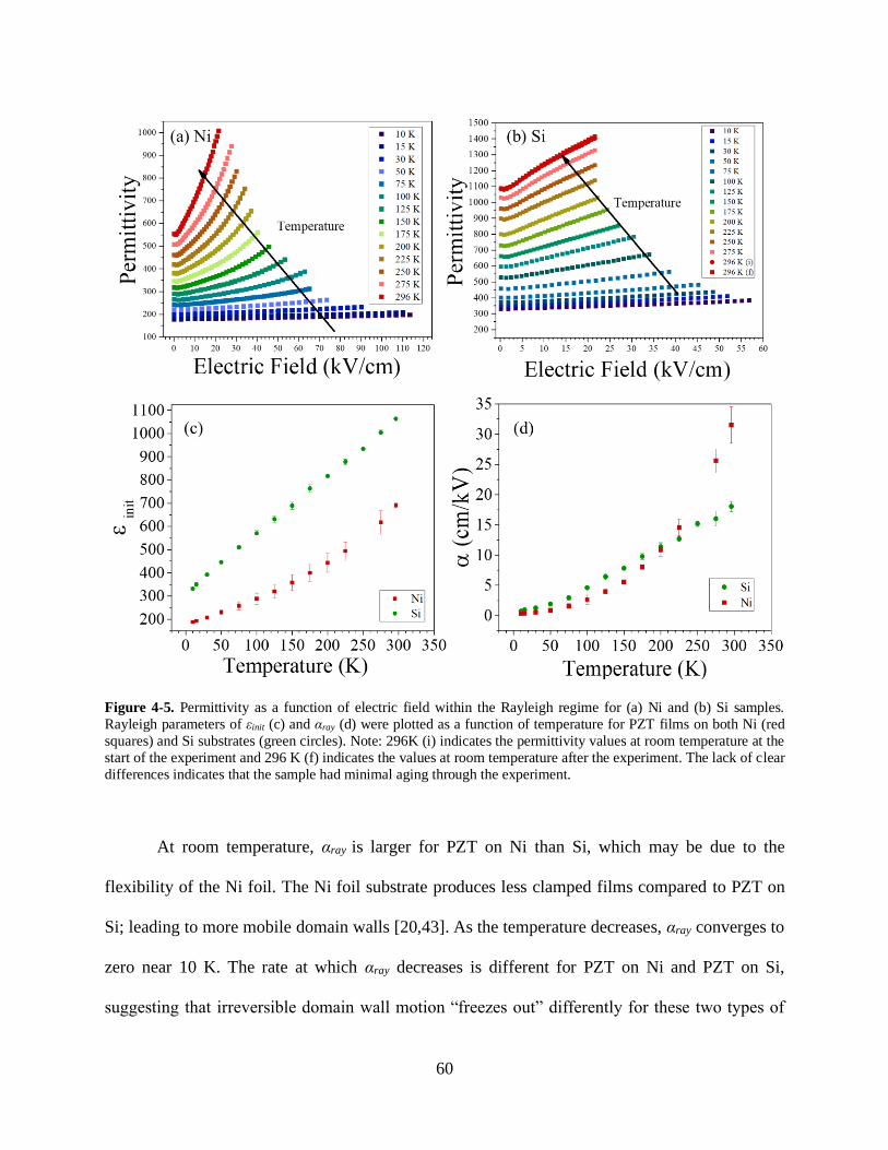
60
Figure 4-5. Permittivity as a function of electric field within the Rayleigh regime for (a) Ni and (b) Si samples.
Rayleigh parameters of εinit (c) and αray (d) were plotted as a function of temperature for PZT films on both Ni (red
squares) and Si substrates (green circles). Note: 296K (i) indicates the permittivity values at room temperature at the
start of the experiment and 296 K (f) indicates the values at room temperature after the experiment. The lack of clear
differences indicates that the sample had minimal aging through the experiment.
At room temperature, αray is larger for PZT on Ni than Si, which may be due to the
flexibility of the Ni foil. The Ni foil substrate produces less clamped films compared to PZT on
Si; leading to more mobile domain walls [20,43]. As the temperature decreases, αray converges to
zero near 10 K. The rate at which αray decreases is different for PZT on Ni and PZT on Si,
suggesting that irreversible domain wall motion “freezes out” differently for these two types of
61
samples. At 10 K, αray is 0.33 ± 0.01 cm/kV for PZT on Ni and 0.56 ± 0.03 cm/kV for PZT on Si.
For temperatures below 200 K, αray is higher for PZT films on Si relative to Ni, but this order
reverses near room temperature.
To investigate the differences in the irreversible contribution, the αRay/εinit ratio was
determined for the two samples in Figure 4-7. These differences in αray and αRay/εinit as a function
of temperature could be due to either differences in the domain structure or differences in the
energy barrier height distribution. It is estimated that PZT on Si has roughly 40-60% “c” domains,
and PZT on Ni has a higher percentage of “c” domains (around 80-95%) [44,64,115]. Thus, it is
likely that PZT films on Si have more non-180° domain walls. Since any motion of non-180°
domain walls produce a large change in permittivity (as “a” and “c” domains have very different
permittivity values), this could account for the higher αray at lower temperatures. However, this
theory would be inconsistent with reports of limited amount of ferroelastic domain wall motion in
films [46,72]. Therefore, it is more likely that there are lower energy barrier heights for PZT on
Si, allowing for a slightly greater αray at lower temperatures. This is also supported by the increase
in the magnitude of stress on the PZT film on Ni (calculated by Equation 4-4). This may cause
increases in pinning centers energies of the PZT on Ni and lead to the larger decay of αray with
temperature.
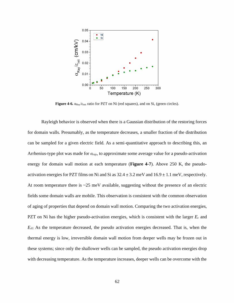
62
Figure 4-6. αRay/εinit ratio for PZT on Ni (red squares), and on Si, (green circles).
Rayleigh behavior is observed when there is a Gaussian distribution of the restoring forces
for domain walls. Presumably, as the temperature decreases, a smaller fraction of the distribution
can be sampled for a given electric field. As a semi-quantitative approach to describing this, an
Arrhenius-type plot was made for αray, to approximate some average value for a pseudo-activation
energy for domain wall motion at each temperature (Figure 4-7). Above 250 K, the pseudo-
activation energies for PZT films on Ni and Si as 32.4 ± 3.2 meV and 16.9 ± 1.1 meV, respectively.
At room temperature there is ~25 meV available, suggesting without the presence of an electric
fields some domain walls are mobile. This observation is consistent with the common observation
of aging of properties that depend on domain wall motion. Comparing the two activation energies,
PZT on Ni has the higher pseudo-activation energies, which is consistent with the larger Ec and
Eδ3. As the temperature decreased, the pseudo activation energies decreased. That is, when the
thermal energy is low, irreversible domain wall motion from deeper wells may be frozen out in
these systems; since only the shallower wells can be sampled, the pseudo activation energies drop
with decreasing temperature. As the temperature increases, deeper wells can be overcome with the
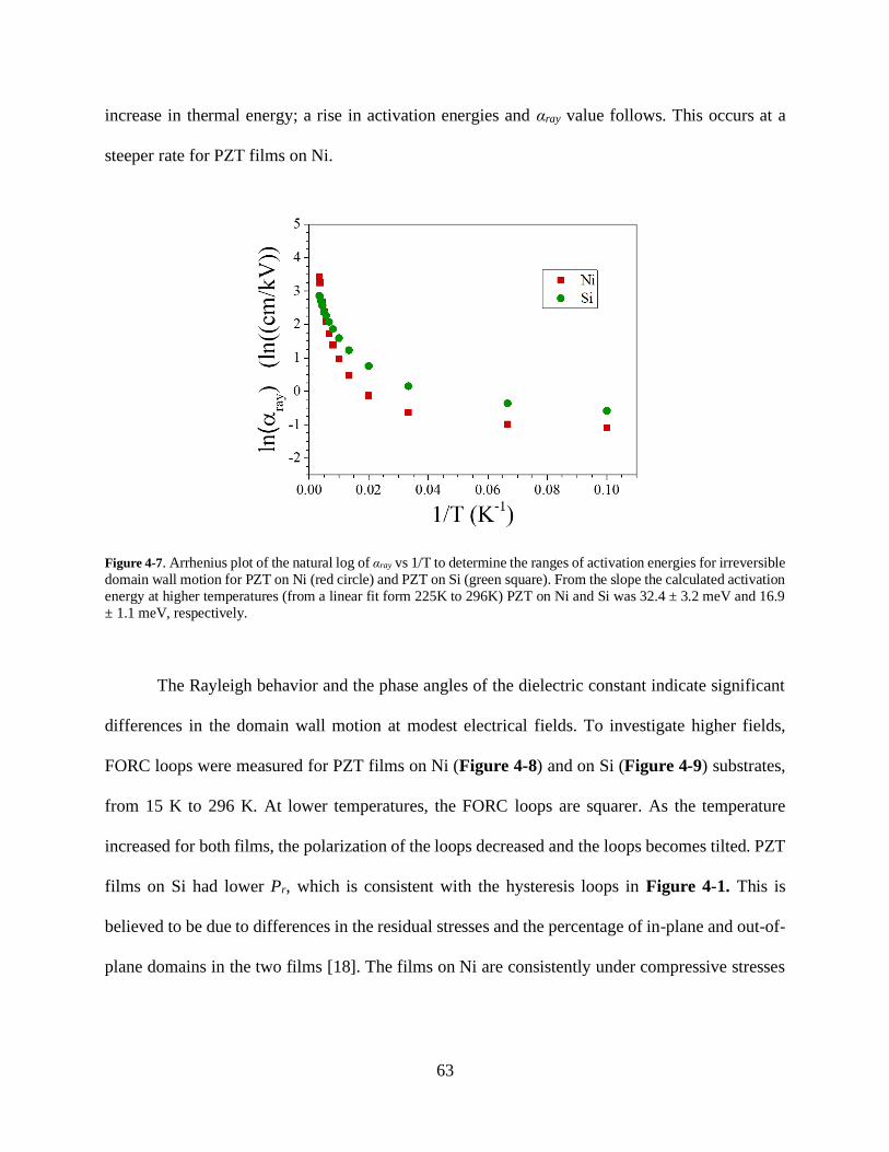
63
increase in thermal energy; a rise in activation energies and αray value follows. This occurs at a
steeper rate for PZT films on Ni.
Figure 4-7. Arrhenius plot of the natural log of αray vs 1/T to determine the ranges of activation energies for irreversible
domain wall motion for PZT on Ni (red circle) and PZT on Si (green square). From the slope the calculated activation
energy at higher temperatures (from a linear fit form 225K to 296K) PZT on Ni and Si was 32.4 ± 3.2 meV and 16.9
± 1.1 meV, respectively.
The Rayleigh behavior and the phase angles of the dielectric constant indicate significant
differences in the domain wall motion at modest electrical fields. To investigate higher fields,
FORC loops were measured for PZT films on Ni (Figure 4-8) and on Si (Figure 4-9) substrates,
from 15 K to 296 K. At lower temperatures, the FORC loops are squarer. As the temperature
increased for both films, the polarization of the loops decreased and the loops becomes tilted. PZT
films on Si had lower Pr, which is consistent with the hysteresis loops in Figure 4-1. This is
believed to be due to differences in the residual stresses and the percentage of in-plane and out-of-
plane domains in the two films [18]. The films on Ni are consistently under compressive stresses
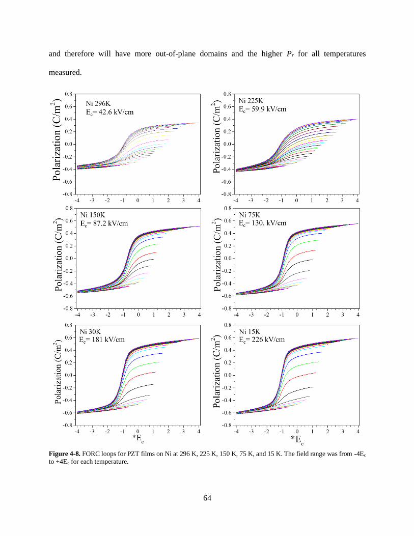
64
and therefore will have more out-of-plane domains and the higher Pr for all temperatures
measured.
Figure 4-8. FORC loops for PZT films on Ni at 296 K, 225 K, 150 K, 75 K, and 15 K. The field range was from -4Ec
to +4Ec for each temperature.
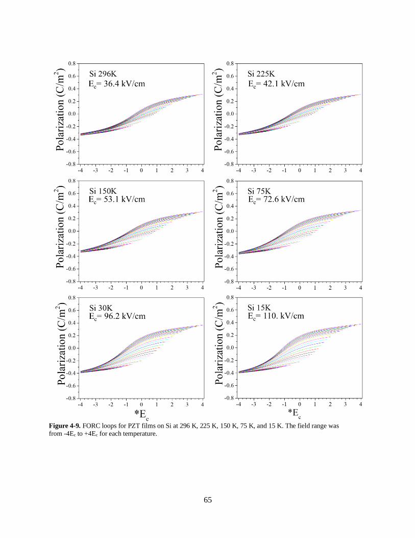
65
Figure 4-9. FORC loops for PZT films on Si at 296 K, 225 K, 150 K, 75 K, and 15 K. The field range was
from -4Ec to +4Ec for each temperature.
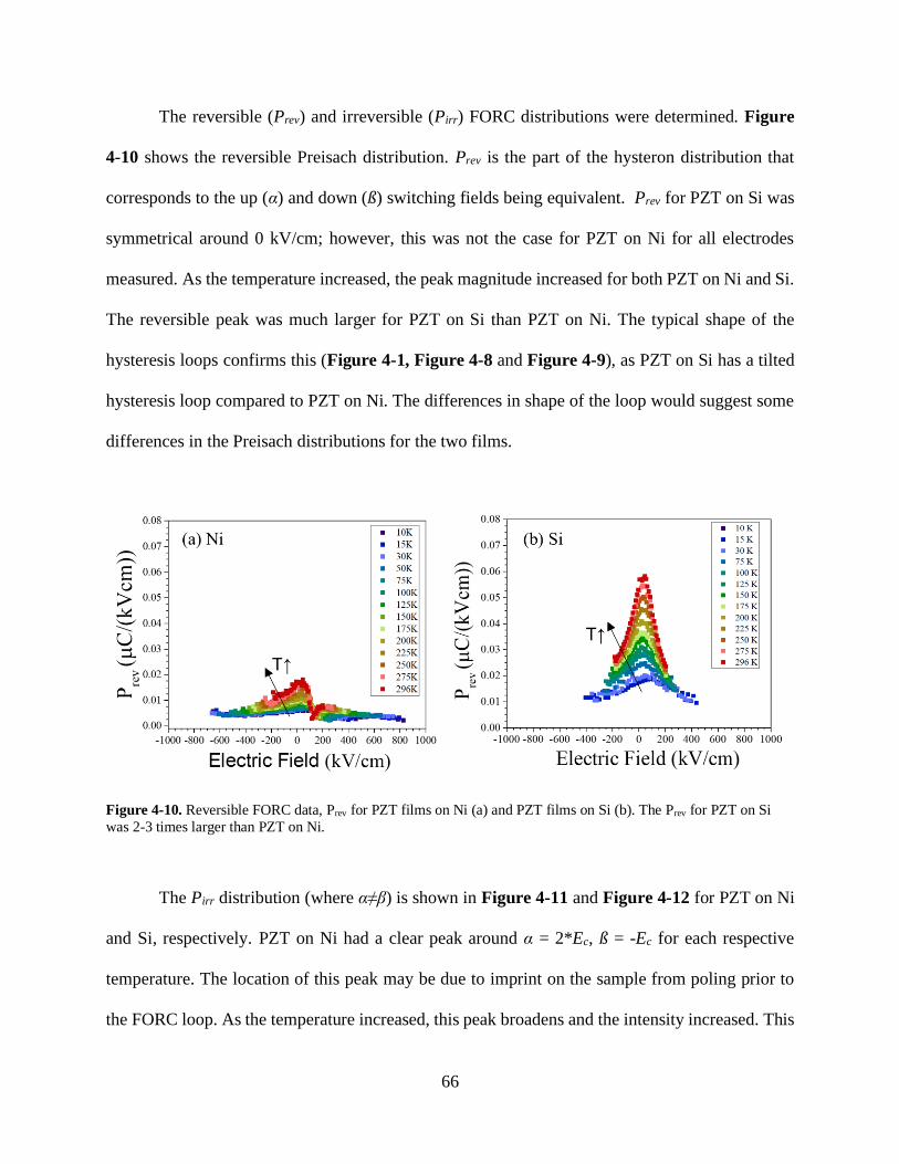
66
The reversible (Prev) and irreversible (Pirr) FORC distributions were determined. Figure
4-10 shows the reversible Preisach distribution. Prev is the part of the hysteron distribution that
corresponds to the up (α) and down (ß) switching fields being equivalent. Prev for PZT on Si was
symmetrical around 0 kV/cm; however, this was not the case for PZT on Ni for all electrodes
measured. As the temperature increased, the peak magnitude increased for both PZT on Ni and Si.
The reversible peak was much larger for PZT on Si than PZT on Ni. The typical shape of the
hysteresis loops confirms this (Figure 4-1, Figure 4-8 and Figure 4-9), as PZT on Si has a tilted
hysteresis loop compared to PZT on Ni. The differences in shape of the loop would suggest some
differences in the Preisach distributions for the two films.
Figure 4-10. Reversible FORC data, Prev for PZT films on Ni (a) and PZT films on Si (b). The Prev for PZT on Si
was 2-3 times larger than PZT on Ni.
The Pirr distribution (where α≠β) is shown in Figure 4-11 and Figure 4-12 for PZT on Ni
and Si, respectively. PZT on Ni had a clear peak around α = 2*Ec, ß = -Ec for each respective
temperature. The location of this peak may be due to imprint on the sample from poling prior to
the FORC loop. As the temperature increased, this peak broadens and the intensity increased. This

67
suggests that as the temperature increases, more hysterons can switch. This is consistent with the
increase in the Prev distribution. It is not clear how individual pinning center’s barrier heights
change with temperature. However, the decrease in residual stress at higher temperatures for PZT
on Ni may change individual barrier heights.
Figure 4-11. Pirrev for PZT on Ni at 296 K (a), 225 K (b), 150 K (c), 75 K (d), 15 K (e). Alpha and Beta are normalized
to 4 times Ec at the reported temperature.
PZT on Si (Figure 4-12) does not show a clear peak but does show a wide distribution of
hysterons (note the scale difference between Figure 4-11 and Figure 4-12). This may suggest
differences in the distribution of barrier heights between PZT on Ni and on Si. The center of Pirr
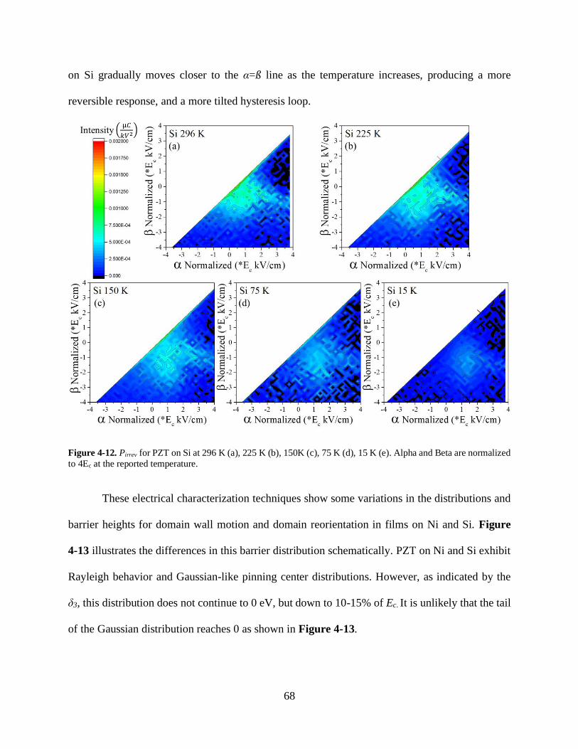
68
on Si gradually moves closer to the α=ß line as the temperature increases, producing a more
reversible response, and a more tilted hysteresis loop.
Figure 4-12. Pirrev for PZT on Si at 296 K (a), 225 K (b), 150K (c), 75 K (d), 15 K (e). Alpha and Beta are normalized
to 4Ec at the reported temperature.
These electrical characterization techniques show some variations in the distributions and
barrier heights for domain wall motion and domain reorientation in films on Ni and Si. Figure
4-13 illustrates the differences in this barrier distribution schematically. PZT on Ni and Si exhibit
Rayleigh behavior and Gaussian-like pinning center distributions. However, as indicated by the
δ3, this distribution does not continue to 0 eV, but down to 10-15% of Ec. It is unlikely that the tail
of the Gaussian distribution reaches 0 as shown in Figure 4-13.
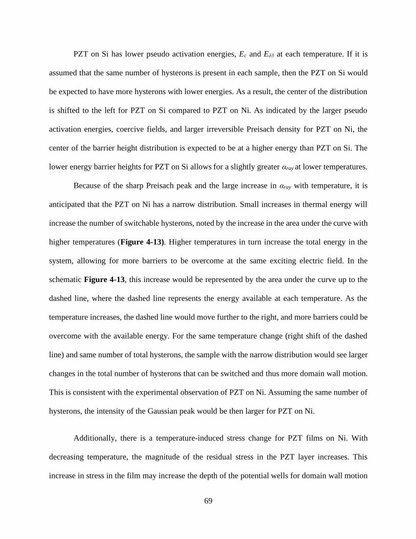
69
PZT on Si has lower pseudo activation energies, Ec and Eδ3 at each temperature. If it is
assumed that the same number of hysterons is present in each sample, then the PZT on Si would
be expected to have more hysterons with lower energies. As a result, the center of the distribution
is shifted to the left for PZT on Si compared to PZT on Ni. As indicated by the larger pseudo
activation energies, coercive fields, and larger irreversible Preisach density for PZT on Ni, the
center of the barrier height distribution is expected to be at a higher energy than PZT on Si. The
lower energy barrier heights for PZT on Si allows for a slightly greater αray at lower temperatures.
Because of the sharp Preisach peak and the large increase in αray with temperature, it is
anticipated that the PZT on Ni has a narrow distribution. Small increases in thermal energy will
increase the number of switchable hysterons, noted by the increase in the area under the curve with
higher temperatures (Figure 4-13). Higher temperatures in turn increase the total energy in the
system, allowing for more barriers to be overcome at the same exciting electric field. In the
schematic Figure 4-13, this increase would be represented by the area under the curve up to the
dashed line, where the dashed line represents the energy available at each temperature. As the
temperature increases, the dashed line would move further to the right, and more barriers could be
overcome with the available energy. For the same temperature change (right shift of the dashed
line) and same number of total hysterons, the sample with the narrow distribution would see larger
changes in the total number of hysterons that can be switched and thus more domain wall motion.
This is consistent with the experimental observation of PZT on Ni. Assuming the same number of
hysterons, the intensity of the Gaussian peak would be then larger for PZT on Ni.
Additionally, there is a temperature-induced stress change for PZT films on Ni. With
decreasing temperature, the magnitude of the residual stress in the PZT layer increases. This
increase in stress in the film may increase the depth of the potential wells for domain wall motion
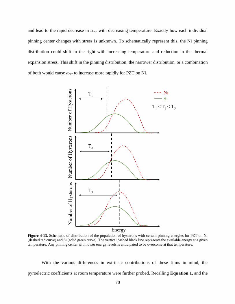
70
and lead to the rapid decrease in αray with decreasing temperature. Exactly how each individual
pinning center changes with stress is unknown. To schematically represent this, the Ni pinning
distribution could shift to the right with increasing temperature and reduction in the thermal
expansion stress. This shift in the pinning distribution, the narrower distribution, or a combination
of both would cause αray to increase more rapidly for PZT on Ni.
Figure 4-13. Schematic of distribution of the population of hysterons with certain pinning energies for PZT on Ni
(dashed red curve) and Si (solid green curve). The vertical dashed black line represents the available energy at a given
temperature. Any pinning center with lower energy levels is anticipated to be overcome at that temperature.
With the various differences in extrinsic contributions of these films in mind, the
pyroelectric coefficients at room temperature were further probed. Recalling Equation 1, and the
71
large differences in π, the different terms of the measured π were determined. The secondary
contribution, which combines stress and piezoelectric contributions, manifests in clamped thin
films as Equation 4-5 from the work of Zook, et al.[130].
𝜋𝑠𝑒𝑐𝑜𝑛𝑑𝑎𝑟𝑦 =2𝑑31(𝛼𝑓−𝛼𝑠)
𝑠11+𝑠12 (4-5)
For PZT on Ni πsecondary was calculated to be approximately -147 µC/m2K, and for PZT on Si,
πsecondary is 45 µC/m2K. The observed pyroelectric coefficient is the sum of the primary, extrinsic,
and secondary term. Therefore, the primary plus extrinsic piece for PZT on Ni would be around -
100 µC/m2K and for PZT on Si would be around -150 µC/m2K. As shown by the larger Pr, PZT
on Ni has more out of plane “c” domains and a larger primary piece. Therefore, for this sum to be
smaller, the film on Ni must have significantly smaller extrinsic piece. This smaller extrinsic term
may be due to higher pinning energies, which is suggested by the various electrical characterization
techniques used in this study and schematically shown in Figure 4-13.
Overall, this study suggests that the distribution of pinning centers for PZT films on Ni and
Si are different; this induces different reversible and irreversible Rayleigh and Preisach
distributions as a function of temperature. Given that the grain sizes are very similar for these two
sets of films, it is believed that the residual stress accounts for at least some of the differences in
the two families of films. Large differences in residual stresses will affect the film’s domain
structure, including the percentage of in-plane and out-of-plane domains and the energy landscape
of various pinning sites for domain wall motion and domain switching. While these extrinsic
contributions are typically considered to account for a small percentage of the total pyroelectric
response, the combined influence of fabrication, stress, temperature on the domain structure and
72
substrate mechanical properties can result in a much more significant impact than one would
expect.
4.4 Conclusions
PZT on Ni has a larger pyroelectric coefficient compared to PZT grown on Si, which is
due to a large secondary contribution. However, the extrinsic contribution may be significantly
reduced due to the residual stresses. PZT on Si and Ni have very different reversible and
irreversible Rayleigh and Preisach coefficients. It is proposed that larger differences in residual
stresses drastically change the film’s domain structure. Stress may allow for differences in the
energy landscape of various pinning sites for domain wall motion and domain switching. These
differences will lead to significant changes in the film’s properties at various temperatures. With
different energy barriers distributions, these films may have different optimal poling and driving
conditions for high device performance. Further study should include defect chemistry,
composition, and thickness on the distributions of pinning sites as well as designing films/substrate
stack with lower energy barrier for domain wall motion to further improve the pyroelectric
coefficient.
73
Chapter 5. Thickness Dependence of Crack Initiation and Propagation in PZT/Si Stacks
Portions of this chapter have been reproduced from: K. Coleman, R. Bermejo, D. Leguillon, and
S. Trolier-McKinstry “Thickness Dependence of Crack Initiation and Propagation in
Piezoelectric Microelectromechanical Stacks” Acta. Mater. 191(2019) 245-252. DOI:
10.1016/j.actamat.2020.03.030
This chapter focuses on determining the relationship between PZT film’s thickness and the
mechanical limits of the PZT film and the stack. PZT/LaNiO3/SiO2/Si stacks with different PZT
thicknesses (from 0.6 to 1.8 µm) were tested using the ball on three ball (B3B) biaxial test method.
Strength distributions of the stacks were evaluated using Weibull statistics and compared to the
reference SiO2/Si samples. The characteristic strength and Weibull modulus were 0 ~1110 MPa
and m ~28, 0 ~1060 MPa and m ~26, and 0 ~880 MPa and m ~10 for the 0.7 µm, 1.3 µm, and
1.8 µm film stack, respectively and 0 ~ 1820 MPa and m ~3 for the substrate as reference. The
effect of PZT thickness on crack initiation was investigated in samples pre-loaded below the stack
failure strength. The crack initiation stress of PZT films depends on the thickness of the PZT layer
as supported by a finite fracture mechanics model. Both experimental data and a linear elastic
fracture mechanics model demonstrate that additional stress is required for the initial crack in the
PZT layer to propagate through the entire stack. These results help predict stress limits for PZT
thin films under pure mechanical loading and provide insight into operational limits for PZT films
under both electrical and mechanical loading, which will be discussed in Chapter 6.
5.1 Introduction
Piezoelectric microelectromechanical systems (piezoMEMS) used in sensors, transducers,
actuators, and energy harvesting devices [1,2] contain multilayer stacks composed of active
piezoelectric layers and their electrodes, with additional layers for adhesion and support. Materials
with high piezoelectric coefficients, such as lead zirconate titanate with a morphotropic phase
74
boundary composition of Pb(Zr0.52Ti0.48)O3 (PZT) [1,2,14] are typically used in order to provide
high sensitivity sensors or large displacement actuators. Additionally, thin piezoelectric layers
(typically between 0.3 and 3 µm in thickness) [16,43,146], are used to significantly reduce the
voltage required to reach target electrical fields, relative to bulk ceramics or single crystals. The
thickness of the piezoelectric layer is optimized to enhance the piezoelectric response and
functionality of the device. For example, thinner films are used for lower voltage applications,
while increasing the thickness of the piezoelectric layer can yield a higher power density for energy
harvesting devices, due to the increase in the active volume [16]. In addition, thicker films tend to
be less clamped to the substrate, which allows for more domain wall motion and may enhance the
piezoelectric response [43,146].
Piezoelectric thin films are typically under significant stress, as discussed in Chapter 3.
The stresses (residual, mechanical, electrical) affect the film’s domain structure and piezoelectric
response [15,18,19], and may also affect the loads (electrical [21] or mechanical [44,72,147]) the
films can withstand. Failure of piezoMEMS stacks typically results from the electromechanical
loading conditions [21,148–150], and has been observed to result in a series of thermal breakdown
events connected through cracks [21,147,148,150,151]. Determining the mechanical limits of
these films is therefore of interest.
Many studies have investigated the mechanical limits of thin films and suggest that the
thickness of the piezoelectric layer may affect the structural integrity of the entire stack; stacks
with thicker layers are more prone to cracking than stacks with thinner films [21]. Previous studies
postulate that the stress required for crack initiation can be a function of thickness either due to a
volume effect in Weibullian materials [152,153] or differences in the residual stress as a function
of thickness [68,154]. To date, the underlying mechanism for crack initiation in piezoMEMS is
75
not well understood. Finite fracture mechanics suggest that the thickness affects the conditions for
crack initiation in the films. Because crack initiation is contingent on the strain energy accumulated
in the film during mechanical loading, it is harder to initiate cracks when the layers are thin [155].
In this work, experimental evidence using Weibull statistics as well as fracture mechanics models
assesses the influence of the piezoelectric layer thickness on the stresses for crack initiation in the
layer and crack propagation through the entire stack.
5.1.1 Weibull Statistics for Failure
Cracking is difficult to predict as microstructure, domain structure [31,84,86,147],
orientation, grain size, and surface quality may influence the mechanical response of the brittle
film [86,156–159]. Additionally, failure may be due to adhesion between layers, interface
properties, and surface condition (e.g. polish, etch, etc.) [157]. Because there may be a large
distribution of flaws, a few measurements may not accurately describe the flaw distributions nor
determine the failure stress.
To experimentally determine a statistically significant strength of a material, Weibull
analysis should be used; this approach is based on the probability 𝑃𝑓(𝜎) that a given stress (σ) is
sufficient for failure, as shown in Equation 5-1 [154,160]
𝑃𝑓(𝜎) = 1 − 𝑒𝑥𝑝 (−(𝜎
𝜎𝑜)𝑚) 5-1
where m is the Weibull modulus and σo is the Weibull strength; the probability of failing at or
below this stress is 63%. When a ceramic has a large distribution of flaw sizes, m will be small
and the confidence interval for the Weibull strength will be large. Weibull analysis can take a three
parameter form: m, σo , and σu, where below σu there is a zero probability of failure [160]. However,

76
for brittle ceramics, Equation 5-1 with two Weibull parameters should be used, since there is a
finite probability that at an infinitesimally small stress could cause failure [160].
5.1.2 Fracture Mechanics
Fracture mechanics models can predict mechanical failure in a material based on the flaws,
geometries, and materials present. Linear elastic fracture mechanics (LEFM) and finite fracture
mechanics (FFM) were used in this study; specifically, mode I failure, where the crack propagates
perpendicular to the tensile stress direction, was employed.
LEFM models treat a crack as a continuous body that propagates continuously [161–164].
Griffith initially modeled the energy balance in the system by considering changes in the internal
energy (elastic stored energy and surface energy) and the work done to the system [162,163,165].
Irwin expanded this to the form in Equation 5-2, which describes the critical stress for cracking,
𝜎𝑐, as being related to the stress intensity factor, 𝐾𝐼𝑐 of the material, knowing the geometry factor,
Y [164]. In LEFM, only the elastic energy of the system is considered; it is presumed that there is
a pre-existing crack of radius a.
𝐾𝐼𝑐 = 𝑌𝜎𝑐√𝜋𝑎 5-2
Because of this assumption, LEFM can only be used to describe conditions for crack propagation
in samples where an initial microcrack already exists [161,166].
To predict crack initiation, the Griffith-Irwin [162,164] criterion for crack propagation is
insufficient; a different approach such as FFM must be considered. FFM states that under applied
mechanical stress, a crack initiates having a “finite” length (which in many cases is on the order
of some characteristic feature in the microstructure) when certain stress and energy conditions are
satisfied [166–169]. FFM utilizes a stress-energy coupled criterion, where a crack originates if two
conditions (i.e. stress and energy conditions) are simultaneously fulfilled.
77
The first condition states that the normal tensile stress ((a)) should be larger than the
material tensile strength (c) along the entire potential crack path ((a) ≥ c). This condition cannot
be the only condition for crack initiation in a material as the stress field at the edge of a notched
flaw would approach infinite and hence would always exceed the strength, causing failure to occur
instantaneously [166]. This extreme case does not occur, so this condition alone is insufficient.
The energy condition, similar to Griffith’s approach, considers the change in the system’s
energy, accounting for the work done to the material and the change in the surface energy due to
creation of a crack as shown in Equation 5-3 [166].
−𝛿𝑊𝑝
𝛿𝑆= 𝐺𝑖𝑛𝑐 (𝑎) ≥ 𝐺𝑐 5-3
where Ginc is the increment of the potential energy for finite crack length increments. The energy
condition for crack initiation is satisfied when Ginc exceeds Gc, the material’s toughness. In the
extreme case of −𝛿𝑊𝑝
𝛿𝑆 → 0 (which corresponds to the case of slow continuous crack growth), Ginc
would never reach the material’s toughness [166]. Therefore, both conditions must be met for
cracks to initiate. When both are met, a crack of defined length will initiate. Additionally, since
the energy criterion depends on the material’s ability to store energy prior to cracking, as the
material’s thickness decreases, a larger amount of energy is required to create new surfaces.
At some thicknesses, the energy criteria will be larger than the strength criteria. As a result,
at small thicknesses the energy criterion determines the crack initiation stress; the magnitude of
this stress depends on the film’s thickness. This criterion has been used to explain the onset of
cracks in thin polymer films on substrates [155,166] or the generation of surface edge cracks in
layered ceramics [170]. In both cases, the potential energy during loading increases with the
thickness of the layer containing the prospective crack. As a result, for the same loading conditions
78
and properties, cracks can initiate in thicker layers under smaller applied loads. Both the FFM and
LEFM models are used in this thesis to predict crack initiation and the subsequent propagation in
PZT thin films.
5.1.3 Overview
This chapter investigates the relationship between PZT film’s thickness and the fracture
response of the stack under mechanical loading. PZT/LaNiO3/SiO2/Si stacks with different PZT
thicknesses were tested in biaxial loading conditions. Strength distributions of the stacks were
evaluated using Weibull statistics and compared to SiO2/Si samples as a reference. The effect of
PZT thickness on crack initiation was investigated in samples pre-loaded below the stack’s failure
strength. Models for crack initiation and for crack propagation are derived based on fracture
mechanics considerations. This study can be used to set structural limits on achievable strains in
piezoMEMS.
5.2 Experimental Procedure:
5.2.1 Sample Preparation and Structural Characterization
Double-side polished 4” Si wafers with a 1 µm thick thermal SiO2 layer on both surfaces
were obtained from Nova Electronic Materials. A 150 nm layer of LaNiO3 (LNO) was deposited
on one surface using an acetic acid based solution, as described in Section 3.2.1 [15,103]. This
layer acts both as a template for {001} orientation of the perovskite structure and as a bottom
electrode. Then, {001} oriented Pb0.99□0.01(Zr0.52Ti0.48)0.98Nb0.02O3 films of 0.7 µm, 1.3 µm, and
1.8 µm were grown by chemical solution deposition (CSD) using a 2-methoxyethanol based
solution, see Section 3.2.1 for more details [15,44,105]. Figure 5-1 shows a schematic of the stack
layers. The orientation and phase purity of the films were characterized by a Merlin FeSEM and
by XRD using a PANalytical Empyrean with a Cu Kα X-Ray source to calculate the Lotgering
79
factor. PZT/LaNiO3/SiO2/Si stacks with different PZT thicknesses, i.e. 0.7 µm, 1.3 µm and 1.8
µm, were diced into 12 x 12 mm squares. Reference samples of the Si substrate with a 1 µm SiO2
layer were also tested for comparison.
Figure 5-1. Schematic of the samples where PZT of varying thicknesses is grown on top of Si wafer.
5.2.2 Ball on Three Ball Biaxial Test Method
The ball on three balls (B3B) biaxial test method was used to determine (i) the strength
distribution of the different samples and (ii) the conditions for crack initiation in the PZT films
[171,172]. In this loading configuration, the rectangular plates are symmetrically supported by
three balls on one face and loaded by a fourth ball in the center of the opposite face (see Figure
5-2); this guarantees well-defined contacts. The four balls had a diameter of 7.5 mm, giving a
support diameter of 8.65 mm. At the midpoint of the plate surface, opposite to the loading ball, a
biaxial tensile stress is generated. One of the main advantages of this method is that the maximal
80
stress developed during the test is located far from the edges (corners) of the sample, i.e. away
from edge defects [171,173–175]. A total of 20 specimens per sample were tested to failure using
a universal tester (Instron, Ma). A pre-load of ~10 N was employed to hold the specimen between
the four balls. Tests were conducted under displacement control of 0.1 mm/min in ambient
conditions (~22°C and ~40% RH). A Weibull statistical analysis was performed according to
ASTM standards [154,160,176].
Figure 5-2. Schematic of the Ball on three Ball (B3B) setup.
The stress at the surface under tension was calculated according to Equation 5-4 [171]:
𝜎𝑓 = 𝑓 ∗𝐹
𝑡2 5-4
where F is the applied force, t is the thickness of the stack, and f is a geometry factor, which
depends on the diameter of the balls, thickness of the sample, and Poisson’s ratio, , of the material.

81
The factor f was calculated using finite element analysis, resulting in f = 2.4 for t = 0.502 mm and
= 0.3. The failure stress (f) was calculated using Equation 5-4, and a homogeneous stress
distribution in the sample during B3B was assumed. However, Equation 5-4 represents the stress
for a homogenous material in the ball on three ball test method. Since the stack used in this study
is a multilayer stack, where over 99% of the stack is Si, it is assumed that the characteristic strength
of the stack is equal to the stress in the top of the Si layer. Si and the various layers have different
mechanical properties such as Young’s modulus. Since the layers above the Si are very thin and
have nearly the same radius of curvature, they have approximately the same strain, but not the
same stress as shown in Equation 5-5.
휀𝑃𝑍𝑇,𝑥 = 휀𝑃𝑍𝑇,𝑦 = 휀𝑆𝑖,𝑥 = 휀𝑆𝑖,𝑦 = 휀𝐿𝑁𝑂,𝑥 = 휀𝐿𝑁𝑂,𝑦 = (𝑠11 + 𝑠12) ∗ 𝑓 ∗𝐹𝑚𝑎𝑥
𝑡2 5-5
Since the films are clamped to the substrate, it is assumed that the 휀𝑧 is close to zero, and
so from the strain determined in Equation 5-5, the stress in the PZT, LNO, or SiO2 layers can be
calculated using the Poisson’s ratio (ν) and Young’s modulus (Y) of the layer. This is given for the
PZT layer in Equation 5-6.
𝜎𝑃𝑍𝑇𝑥,𝑦 =𝐸
1−𝑣(휀𝑃𝑍𝑇,𝑥,𝑦) 5-6
The Young’s modulus for {001} PZT is 90 GPa [93] and Poisson’s ratio has been estimated to be
0.3.
To investigate crack initiation, selected specimens were loaded between 20% and 80% of
the characteristic Weibull stress of the different stacks (loaded in increments of 5%). Each of these
samples was only loaded once. The PZT side of the stack was then imaged using an oversaturated
dark field optical microscope to assess the presence of cracks. The lowest load at which cracking
was observed was recorded as the stress required for crack initiation in the PZT layer. In order to
determine the depth of the surface pre-cracks, a FEI Scios Focused Ion Beam (FIB) system was
82
employed. Cross-sections were made from the top PZT surface down to the SiO2 layer. From these
results, crack initiation and propagation models were developed.
5.3 Results
5.3.1 Microstructure
Figure 5-3 shows the FeSEM and XRD patterns for the different samples. All PZT films
had strong {100} orientation, with comparable Lotgering factors of 99%, 97% and 99% for the 0.7
µm, 1.3 µm, and 1.8 µm PZT films, respectively. The average surface grain size of the 0.7 µm, 1.3
µm, and 1.8 µm PZT film is 86 ± 7 nm, 105 ± 20 nm, and 106 ± 14 nm, respectively. All of these
grain sizes fall within the first standard deviation of each other.
Figure 5-3. XRD pattern of the 0.7 µm PZT (a), 1.3 µm PZT (b), and 1.8 µm PZT on Si (c), where the Lotgering
factor is above 0.96 for all samples. The microstructure top view and cross section of the 0.7 µm (d and g respectively),
1.3 µm (e and h respectively), and 1.8 µm PZT sample (f and i respectively). The average grain size (diameter) of the
0.7 µm, 1.3 µm, and 1.8 µm PZT film is 86 ± 7 nm, 105 ± 20 nm, and 106 ± 14 nm, respectively.

83
5.3.2 Strength distribution
Figure 5-4 shows the strength distribution of the different sample sets represented as a
Weibull diagram; the corresponding characteristic strength, 0, and Weibull moduli, m, are also
tabulated in Table 5-1 along with the 90% confidence intervals. It is apparent that the SiO2/Si/SiO2
substrates have the highest characteristic strength (0 ~ 1815 MPa) and the lowest Weibull
modulus (m ~ 3). Si substrates tend to have a broad population of critical flaw sizes [157–
159,174,177,178], which is consistent with the low Weibull modulus observed in this study. The
Weibull strength decreases with the addition of the thin PZT/LaNiO3 layers. That is, the PZT layer
reduces the strength of the stack [173,174]. It is also apparent that stacks with thinner PZT layers
have higher characteristic strength than stacks with thicker PZT layers, i.e. 0 ~ 1114 MPa for the
0.7 µm film, 0 ~ 1063 MPa for the 1.3 µm film, and 0 ~ 875 MPa for the 1.8 µm film. Moreover,
the stacks with the PZT layers have higher Weibull moduli than the Si substrate itself, suggesting
failure from a narrower distribution of critical flaw sizes in the former.
84
Figure 5-4. The Weibull plot for the following samples: SiO2/Si (blue circle), 1.8 µm PZT on LaNiO3/SiO2/Si (red
square), 1.3 µm PZT on LaNiO3/SiO2/Si (orange downward triangle), and 0.7 µm PZT on LaNiO3/SiO2/Si (green
upward triangle). The Weibull strength and Weibull modulus varied with the thickness of the PZT film on the Si
wafer.
Table 5-1. Characteristic load, characteristic strength, and Weibull modulus for the PZT/Si stacks of various
thicknesses and the Si substrate. All stress values are in MPa and are calculated for the stress in the Si layer upon
failure. Brackets represent 90% confidence intervals.
Sample Characteristic
Load, F0 (N)
Characteristic
Strength, 0 (MPa)
Weibull
Modulus, m (-)
Si
(w/ 1 µm SiO2 )
190
[165 – 216]
1815
[1588 – 2081]
3
[2 – 4]
Si- 0.7 µm PZT 116
[114 – 117]
1114
[1097 – 1131]
28
[19 – 35]
Si-1.3 µm PZT 111
[109 – 112]
1063
[1047 – 1082]
26
[18 – 33]
Si- 1.8 µm PZT 92
[87 – 95]
875
[839 – 912]
10
[7 – 13]
85
5.3.3 Crack initiation
The total force required to crack the PZT layer was (i) 64 N for the 0.7 µm film, (ii) 56 N
and higher for the 1.3 µm film, and (iii) 49 N and higher for the 1.8 µm films. Figure 5-5 shows
oversaturated dark field optical images from the center of selected specimens pre-loaded at lower
stress levels (between 40% and 80%) than the characteristic strength of the stack. At lower loads
(20-40%), cracking was not present. The stress in the stack was determined from Equation 5-4,
and the stress in the PZT layer (labeled in Figure 5-5) was calculated from Equation 5-6, with the
addition of 150 MPa of tensile residual stress in the PZT [44,93,178], which was measured by the
wafer curvature method. The total stress required for crack initiation was 590 ± 29 MPa, 540 ± 29
MPa, and 490 ± 29 MPa, for the 0.7, 1.3, and 1.8 µm films, respectively. The initial cracks did not
cause fracture of the entire stack, which was still intact upon unloading. These initial cracks were
only visible on the PZT side and were concentrated near the center of the sample, where the
maximum tensile stress was applied.
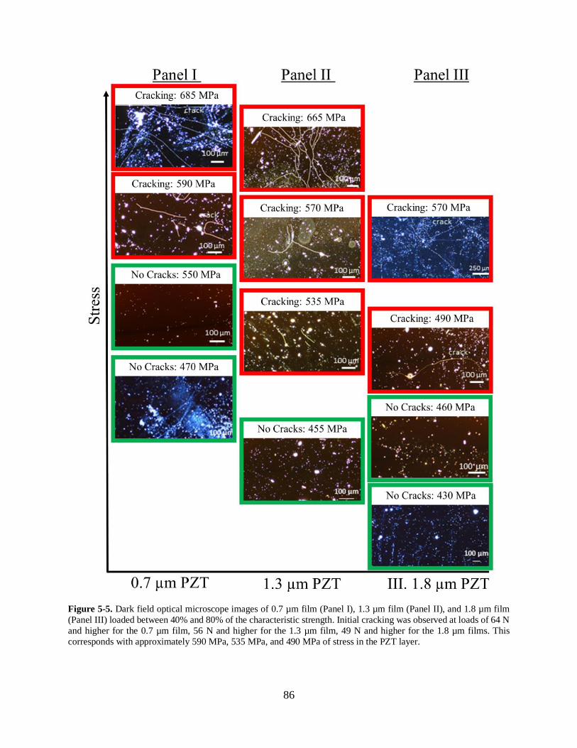
86
Figure 5-5. Dark field optical microscope images of 0.7 µm film (Panel I), 1.3 µm film (Panel II), and 1.8 µm film
(Panel III) loaded between 40% and 80% of the characteristic strength. Initial cracking was observed at loads of 64 N
and higher for the 0.7 µm film, 56 N and higher for the 1.3 µm film, 49 N and higher for the 1.8 µm films. This
corresponds with approximately 590 MPa, 535 MPa, and 490 MPa of stress in the PZT layer.
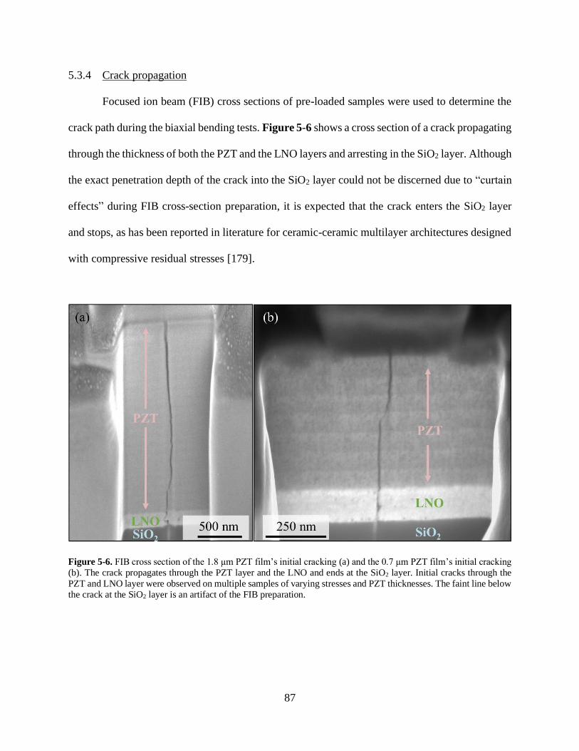
87
5.3.4 Crack propagation
Focused ion beam (FIB) cross sections of pre-loaded samples were used to determine the
crack path during the biaxial bending tests. Figure 5-6 shows a cross section of a crack propagating
through the thickness of both the PZT and the LNO layers and arresting in the SiO2 layer. Although
the exact penetration depth of the crack into the SiO2 layer could not be discerned due to “curtain
effects” during FIB cross-section preparation, it is expected that the crack enters the SiO2 layer
and stops, as has been reported in literature for ceramic-ceramic multilayer architectures designed
with compressive residual stresses [179].
Figure 5-6. FIB cross section of the 1.8 µm PZT film’s initial cracking (a) and the 0.7 µm PZT film’s initial cracking
(b). The crack propagates through the PZT layer and the LNO and ends at the SiO2 layer. Initial cracks through the
PZT and LNO layer were observed on multiple samples of varying stresses and PZT thicknesses. The faint line below
the crack at the SiO2 layer is an artifact of the FIB preparation.

88
5.4 Discussion
5.4.1 Residual stresses
The stress required to initiate a crack in the PZT/LNO layers depends on the thickness of
the PZT film. Thinner films require higher total stresses for crack initiation than either thicker
films or bulk PZT ceramics [180]. The experimental residual stress is reported to be constant for
PZT films above 350 nm thickness [68], which is consistent with calculations shown in
Table 5-2. Therefore, it is unlikely that the differences in crack initiation stress between
samples can be accounted for by a difference in the residual stress.
Table 5-2. In-plane residual stresses calculated in each of the layers.
Sample Residual stress in layer (MPa)
PZT LNO SiO2 Si
0.7 µm +192 +622 -265 +0.2
1.3 µm +192 +622 -265 +0.2
1.8 µm +192 +621 -266 -0.6
5.4.2 Weibull volume effect
Another hypothesis is related to the Weibull volume effect [154]: larger material volumes
loaded under the same applied tensile stress have a higher probability of failure than smaller
volumes in Weibull materials. That is, the characteristic strength, i, of a sample with volume Vi,
can be calculated based on the characteristic strength, o, measured on a reference volume Vo, and
the Weibull modulus of the material, m, according to Equation 5-7 [153,154,160]:
𝜎𝑖 = 𝜎𝑜 (𝑉𝑜
𝑉𝑖)
1
𝑚 5-7
In this work, the probability of failure from a critical flaw in samples with thinner PZT films should
be lower.
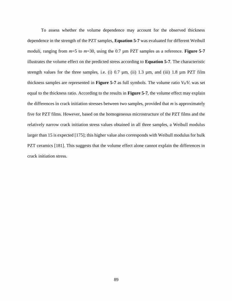
89
To assess whether the volume dependence may account for the observed thickness
dependence in the strength of the PZT samples, Equation 5-7 was evaluated for different Weibull
moduli, ranging from m=5 to m=30, using the 0.7 µm PZT samples as a reference. Figure 5-7
illustrates the volume effect on the predicted stress according to Equation 5-7. The characteristic
strength values for the three samples, i.e. (i) 0.7 µm, (ii) 1.3 µm, and (iii) 1.8 µm PZT film
thickness samples are represented in Figure 5-7 as full symbols. The volume ratio V0/Vi was set
equal to the thickness ratio. According to the results in Figure 5-7, the volume effect may explain
the differences in crack initiation stresses between two samples, provided that m is approximately
five for PZT films. However, based on the homogeneous microstructure of the PZT films and the
relatively narrow crack initiation stress values obtained in all three samples, a Weibull modulus
larger than 15 is expected [175]; this higher value also corresponds with Weibull modulus for bulk
PZT ceramics [181]. This suggests that the volume effect alone cannot explain the differences in
crack initiation stress.
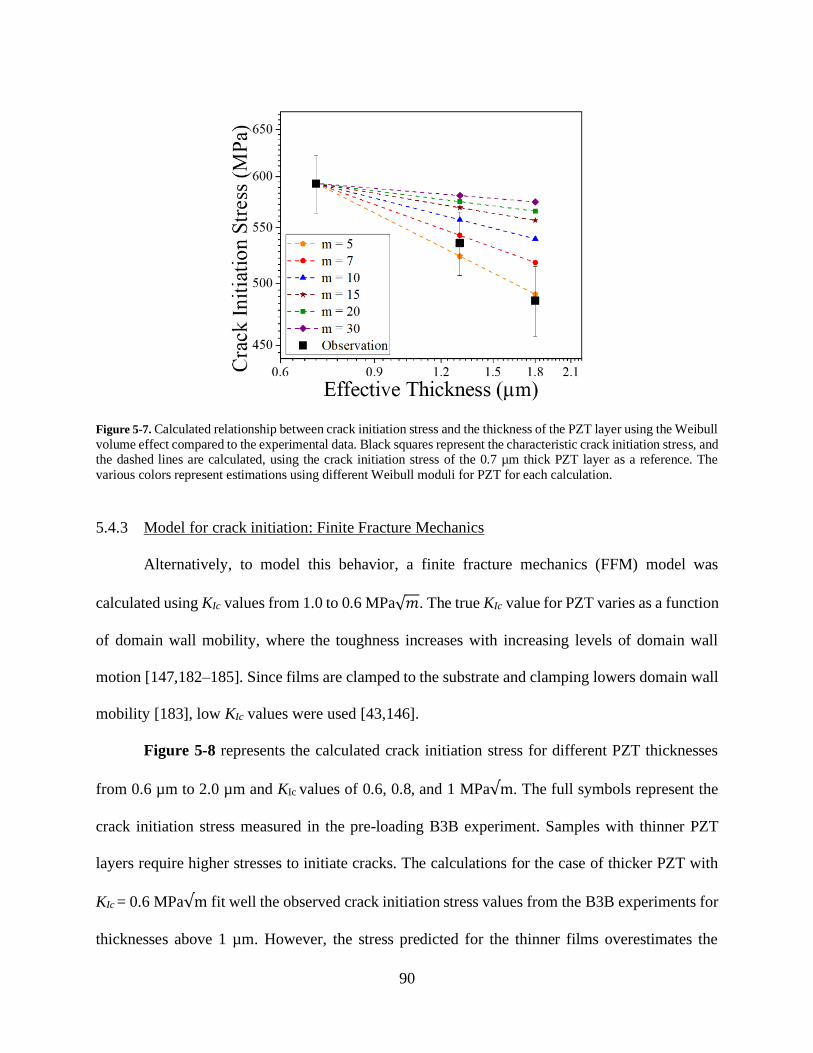
90
Figure 5-7. Calculated relationship between crack initiation stress and the thickness of the PZT layer using the Weibull
volume effect compared to the experimental data. Black squares represent the characteristic crack initiation stress, and the dashed lines are calculated, using the crack initiation stress of the 0.7 µm thick PZT layer as a reference. The
various colors represent estimations using different Weibull moduli for PZT for each calculation.
5.4.3 Model for crack initiation: Finite Fracture Mechanics
Alternatively, to model this behavior, a finite fracture mechanics (FFM) model was
calculated using KIc values from 1.0 to 0.6 MPa√𝑚. The true KIc value for PZT varies as a function
of domain wall mobility, where the toughness increases with increasing levels of domain wall
motion [147,182–185]. Since films are clamped to the substrate and clamping lowers domain wall
mobility [183], low KIc values were used [43,146].
Figure 5-8 represents the calculated crack initiation stress for different PZT thicknesses
from 0.6 µm to 2.0 µm and KIc values of 0.6, 0.8, and 1 MPa√m. The full symbols represent the
crack initiation stress measured in the pre-loading B3B experiment. Samples with thinner PZT
layers require higher stresses to initiate cracks. The calculations for the case of thicker PZT with
KIc = 0.6 MPa√m fit well the observed crack initiation stress values from the B3B experiments for
thicknesses above 1 µm. However, the stress predicted for the thinner films overestimates the
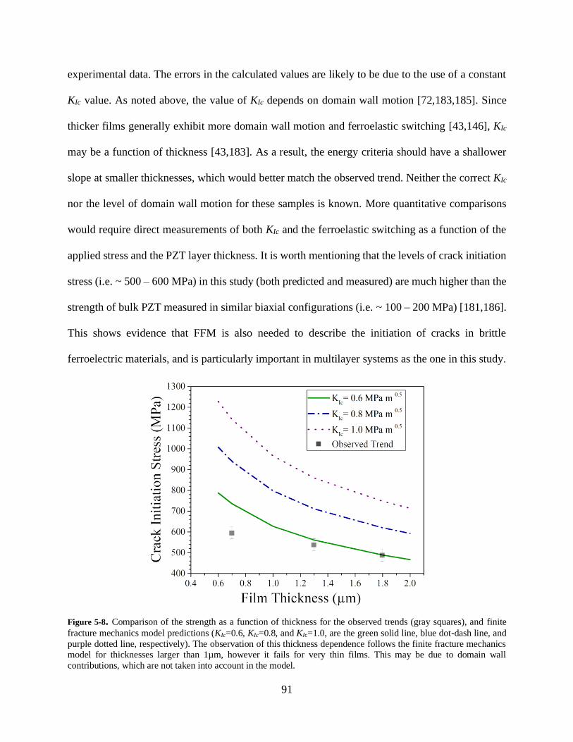
91
experimental data. The errors in the calculated values are likely to be due to the use of a constant
KIc value. As noted above, the value of KIc depends on domain wall motion [72,183,185]. Since
thicker films generally exhibit more domain wall motion and ferroelastic switching [43,146], KIc
may be a function of thickness [43,183]. As a result, the energy criteria should have a shallower
slope at smaller thicknesses, which would better match the observed trend. Neither the correct KIc
nor the level of domain wall motion for these samples is known. More quantitative comparisons
would require direct measurements of both KIc and the ferroelastic switching as a function of the
applied stress and the PZT layer thickness. It is worth mentioning that the levels of crack initiation
stress (i.e. ~ 500 – 600 MPa) in this study (both predicted and measured) are much higher than the
strength of bulk PZT measured in similar biaxial configurations (i.e. ~ 100 – 200 MPa) [181,186].
This shows evidence that FFM is also needed to describe the initiation of cracks in brittle
ferroelectric materials, and is particularly important in multilayer systems as the one in this study.
Figure 5-8. Comparison of the strength as a function of thickness for the observed trends (gray squares), and finite
fracture mechanics model predictions (KIc=0.6, KIc=0.8, and KIc=1.0, are the green solid line, blue dot-dash line, and
purple dotted line, respectively). The observation of this thickness dependence follows the finite fracture mechanics
model for thicknesses larger than 1µm, however it fails for very thin films. This may be due to domain wall
contributions, which are not taken into account in the model.
92
5.4.4 Model for crack propagation: Linear Fracture Mechanics
Based on the experimental observations (Figure 5-5 and Figure 5-6), crack initiation in
the PZT film is followed by crack propagation and arrest at the SiO2 layer. This occurs in the 0.7
µm, 1.3 µm, and 1.8 µm PZT film samples. Crack arrest in the SiO2 may be explained either by a
significant change in the crack growth resistance of the material as the crack advances (referred to
as R-curve behavior [163]) or due to shielding effects associated with compressive residual stresses
in the layer. In this system the R-curve behavior does not apply, because the fracture toughness of
SiO2 does not change with the crack length, and has been reported to be ~ 0.85 MPa√m [159]. The
presence of compressive residual stresses however may hinder crack propagation, depending on
the magnitude of stress and layer thickness, as has been demonstrated for instance in layered
ceramics [179]. The conditions for crack propagation compare the stress intensity factor at the
crack tip during loading with the crack growth resistance in the layer where the tip of the crack is
located. The stress intensity factor at the crack tip is a function of the crack length, Ktip(a), and can
be given as the externally applied stress intensity factor Kappl(a) plus the contribution of the residual
stresses:
𝐾𝑡𝑖𝑝 (𝑎) = 𝐾𝑎𝑝𝑝𝑙 (𝑎) + 𝐾𝑟𝑒𝑠 (𝑎) 5-8
Kappl(a) can be calculated according to the Griffith criterion based on LEFM, where [162,164]:
𝐾𝑎𝑝𝑝𝑙 (𝑎) = 𝜎𝑎𝑝𝑝𝑙𝑌√𝑎 5-9
with σappl being the stress applied during loading. The term Kres(a) represents the residual stress
intensity factor as a function of the position of the crack tip within the corresponding layer in the
stack. In order to account for the contribution of residual stresses through the multilayer stack, a
weight function analysis was employed [179]. The weighting function is related to the crack
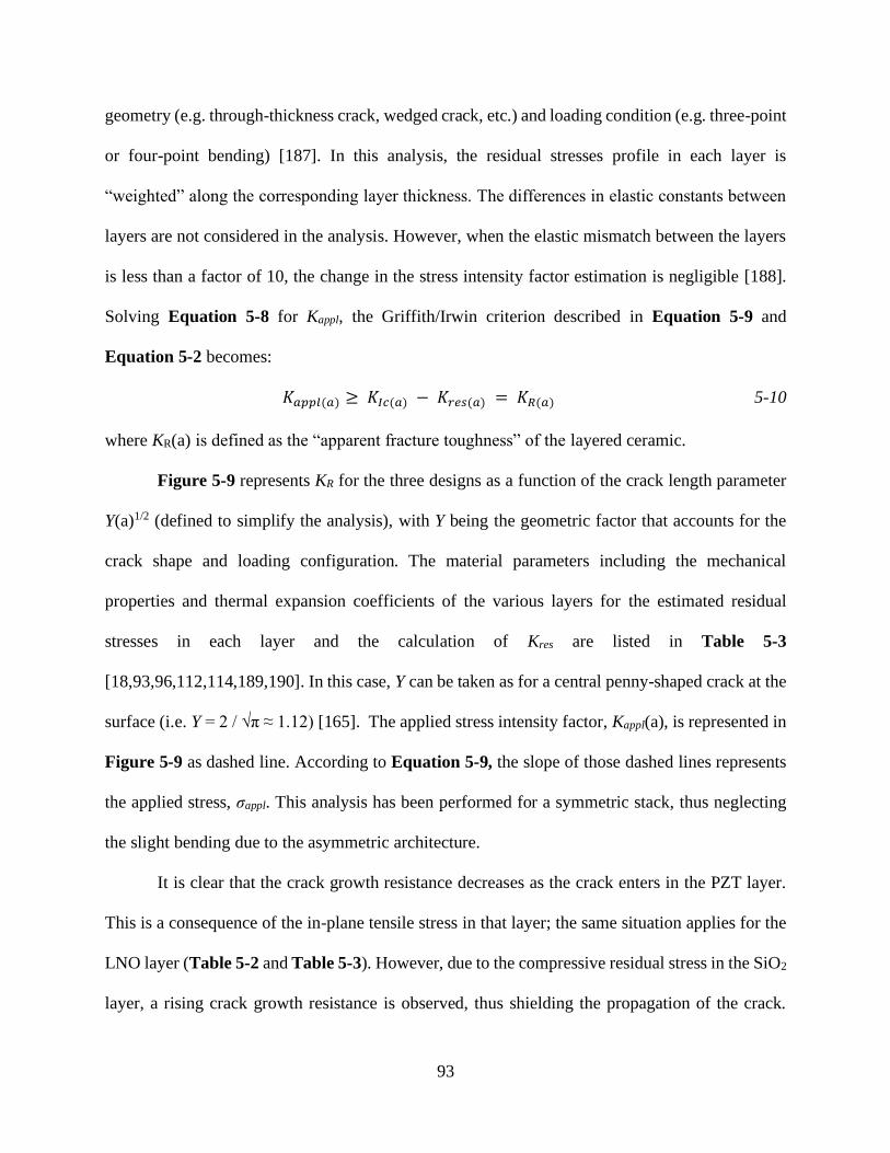
93
geometry (e.g. through-thickness crack, wedged crack, etc.) and loading condition (e.g. three-point
or four-point bending) [187]. In this analysis, the residual stresses profile in each layer is
“weighted” along the corresponding layer thickness. The differences in elastic constants between
layers are not considered in the analysis. However, when the elastic mismatch between the layers
is less than a factor of 10, the change in the stress intensity factor estimation is negligible [188].
Solving Equation 5-8 for Kappl, the Griffith/Irwin criterion described in Equation 5-9 and
Equation 5-2 becomes:
𝐾𝑎𝑝𝑝𝑙(𝑎) ≥ 𝐾𝐼𝑐(𝑎) − 𝐾𝑟𝑒𝑠(𝑎) = 𝐾𝑅(𝑎) 5-10
where KR(a) is defined as the “apparent fracture toughness” of the layered ceramic.
Figure 5-9 represents KR for the three designs as a function of the crack length parameter
Y(a)1/2 (defined to simplify the analysis), with Y being the geometric factor that accounts for the
crack shape and loading configuration. The material parameters including the mechanical
properties and thermal expansion coefficients of the various layers for the estimated residual
stresses in each layer and the calculation of Kres are listed in Table 5-3
[18,93,96,112,114,189,190]. In this case, Y can be taken as for a central penny-shaped crack at the
surface (i.e. Y = 2 / √π ≈ 1.12) [165]. The applied stress intensity factor, Kappl(a), is represented in
Figure 5-9 as dashed line. According to Equation 5-9, the slope of those dashed lines represents
the applied stress, σappl. This analysis has been performed for a symmetric stack, thus neglecting
the slight bending due to the asymmetric architecture.
It is clear that the crack growth resistance decreases as the crack enters in the PZT layer.
This is a consequence of the in-plane tensile stress in that layer; the same situation applies for the
LNO layer (Table 5-2 and Table 5-3). However, due to the compressive residual stress in the SiO2
layer, a rising crack growth resistance is observed, thus shielding the propagation of the crack.
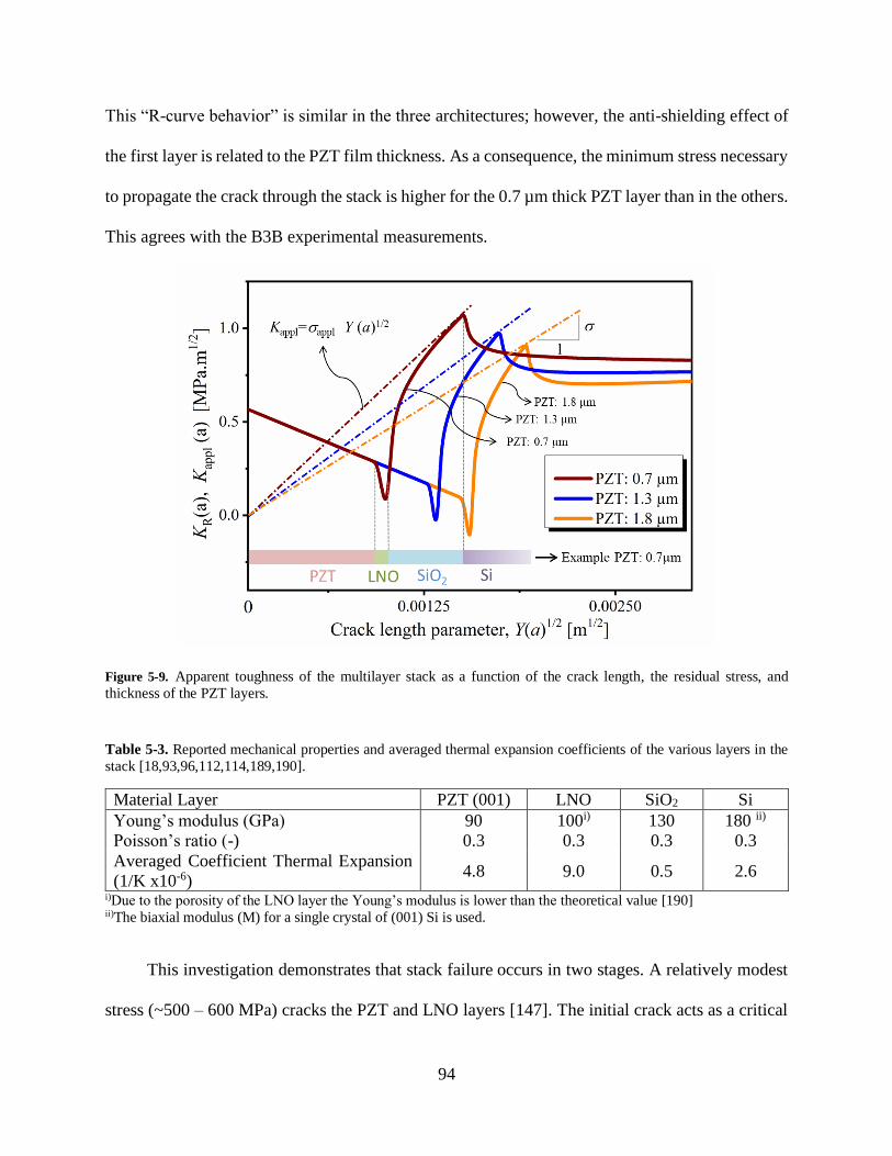
94
This “R-curve behavior” is similar in the three architectures; however, the anti-shielding effect of
the first layer is related to the PZT film thickness. As a consequence, the minimum stress necessary
to propagate the crack through the stack is higher for the 0.7 µm thick PZT layer than in the others.
This agrees with the B3B experimental measurements.
Figure 5-9. Apparent toughness of the multilayer stack as a function of the crack length, the residual stress, and
thickness of the PZT layers.
Table 5-3. Reported mechanical properties and averaged thermal expansion coefficients of the various layers in the
stack [18,93,96,112,114,189,190].
Material Layer PZT (001) LNO SiO2 Si
Young’s modulus (GPa) 90 100i) 130 180 ii)
Poisson’s ratio (-) 0.3 0.3 0.3 0.3
Averaged Coefficient Thermal Expansion
(1/K x10-6) 4.8 9.0 0.5 2.6
i)Due to the porosity of the LNO layer the Young’s modulus is lower than the theoretical value [190] ii)The biaxial modulus (M) for a single crystal of (001) Si is used.
This investigation demonstrates that stack failure occurs in two stages. A relatively modest
stress (~500 – 600 MPa) cracks the PZT and LNO layers [147]. The initial crack acts as a critical

95
flaw for the failure of the SiO2/Si substrate. As the initial cracks are of consistent length (the sum
of the PZT and LNO thicknesses) and the fracture toughness of SiO2 is constant, the stack fails at
a consistent stress level for a given PZT thickness. This, in turn, produces the higher Weibull
modulus of the PZT stack relative to the SiO2/Si substrate itself. This model also accounts for the
observation that the Weibull characteristic strength drops as the PZT thickness increases. That is,
thinner PZT layers display shorter initial crack lengths and require higher stresses to propagate the
crack through the SiO2 layer.
5.5 Conclusions
The thickness of PZT films employed in piezoMEMS has a significant influence on the crack
onset and fracture resistance of the entire stack. Biaxial strength measurements on stacks
containing different PZT layers grown on 500 µm Si substrates showed a decrease in the
characteristic strength, 0, with the PZT layer thickness, ranging from 0 ~ 1110 MPa for 0.7 µm
thin film stacks, to 0 ~ 1060 MPa for the 1.3 µm thin film stack, and 0 ~ 880 MPa for the 1.8
µm film stack. These values were significantly lower than the strength of the Si substrate, i.e. 0
~ 1820 MPa. The higher Weibull modulus obtained in the PZT/Si stacks (i.e. m ~ 28 for the 0.7
µm thin film stack, m ~ 26 for the 1.3 µm thin film stack, and m ~ 10 for the 1.8 µm film stack)
compared to Si substrate (i.e. m ~ 3) suggests that the PZT/LNO layer thickness becomes the
critical flaw size for failure of the entire stack. A stress-energy criterion based on FFM was
employed to explain the higher applied load necessary to initiate cracks in the stack containing a
thinner PZT layer. Biaxial tests to pre-crack the stacks showed the same trend as the model. This
coupled criterion for crack initiation may be extended to complex ferroic materials, if the domain
responses are taken into account. Indeed, this could ultimately become a method to quantitatively
understand domain wall mobility in ferroic structures under stress. In addition, observation of
96
crack arrest within the multilayer structure prior to the fracture of the entire stack suggests the
possibility of tailoring the internal architecture of piezoMEMS to enhance mechanical integrity
and thus performance.

97
Chapter 6. Effect of Electromechanical Loads on Failure Limits of PZT thin Films
Portions of this chapter have been reproduced from:
K. Coleman, J. Walker, W. Zhu, S.W. Ko, P. Mardilovich, and S. Trolier-McKinstry “Failure
mechanisms of lead zirconate titanate thin films during electromechanical loading” in prep
M. Ritter, K. Coleman, R. Bermejo, and S. Trolier-McKinstry “Mechanical Failure
Dependence on the Electrical History of Lead Zirconate Titanate Thin Films” submitted (2020)
This chapter evaluates the effects of electromechanical loading and electrical history of a lead
zirconate titanate (PZT) layer on the failure behavior. First, 0.6 µm PZT films with different in-
plane stress states were failed electromechanically, and the failure patterns revealed that thermal
breakdown events and cracks were connected, suggesting coupling between electrical and
mechanical failure. Additionally, cracking was observed at 480 ± 50 MPa, which is lower than the
reported crack initiation stress for films with similar thickness (590 ± 29 MPa) in Chapter 5. To
understand the reduction in crack initiation stress, Ball-on-three Balls (B3B) testing of PZT films
with variations in electric history (virgin, poled, and under DC bias samples) was employed. The
crack initiation stress depended on the electrical history of the sample and was highest for the
virgin samples (0 ~ 485 ± 30 MPa). The films under DC bias had their relative permittivity and
loss tangent measured in situ in the B3B set up. Changes in the permittivity suggests
electromechanical loading conditions can destabilize the domain structure.
6.1 Introduction
In many piezoMEMS applications, PZT thin films are subjected to severe
electromechanical loading conditions to achieve high power outputs, signal strengths, and device
efficiencies. In sensors and energy harvesters, the mechanical strains applied can be large, and for
thin film actuators, the applied electric fields are usually much larger than those experienced by
98
their bulk counterparts [16,191,192]. Electromechanical failure of piezoelectric thin films is thus
a common topic of considerable technological and commercial significance.
In order to guarantee high performance of the stack, the structural integrity of the film
must also be preserved during electromechanical service conditions. Due to the inherent brittleness
of PZT, cracking of the film layers is a common problem, leading to a degradation of the electrical
properties of the stack or complete failure [147–149]. Recent studies have shown that failure of the
stack under electrical load begins with cracking in the PZT films [21,148–150]. Electric field
induced cracking is believed to be a result of electrically induced stress (σe) in the film, which
depends on the piezoelectric response (e31,f) and the electrostrictive response shown in Equation
3-6. For PZT thin films, it is assumed that since e31,f is much greater than M, the electrostrictive
term can be ignored, as shown in Equation 6-1.
𝜎𝑝 = −𝑒31,𝑓 𝐸 (6-1)
Equation 6-1 points out a fundamental dilemma for piezoMEMS engineers; while a larger e31,f is
desirable for increased device output and efficiency, a larger e31,f also results in larger σp at a given
electric field (E).
Many initial studies have attempted to quantify the total stresses required for crack
initiation and propagation [21,147,150]. For PZT thin films, cracks will initiate between
approximately 0.5 and 1 GPa [147], which is considerably larger than for bulk PZT, in which both
tensile and bending strength is reach around 50-100 MPa [193,194]. Chapter 5 explores the crack
initiation stresses for PZT films under pure mechanical load and suggests that the crack initiation
stress in PZT films depends on the film thickness [138,147]. Thicker films need less stress for
failure [138,166] due to an energy criterion, which states the required energy in the system
99
(potential energy and work on the system) needs to exceed the surface energy required for creating
a crack [166].
Missing in the literature is work that quantifies the onset of cracking in either poled or
electromechanically loaded PZT thin films. It is well known that under applied electric fields, the
domain structure will change, which in turn causes reorientation of the spontaneous strain.
Although this effect is more pronounced for piezoelectric ceramics [183–185], small changes in
the ferroelastic domain structure have been reported in piezoelectric thin films [44,72]. This
chapter investigates how in-plane stresses and electrical history affect the fracture behavior of PZT
films, and also explores how mechanical loads can affect the PZT film’s permittivity.
6.2 Influence of Uniaxial Strains on Electromechanical Failure
In this section, the failure pattern of electromechanically loaded PZT films under different
was explored. The anisotropy in the in-plane stress was created by using the beam bending method
(Section 3.2.4). The films used in this study were also used in Chapter 3. The 0.6 µm thick
Pb0.99(Zr0.52Ti0.48)0.98Nb0.02O3 films were made through chemical solution deposition on
LaNiO3/SiO2/Si wafers (Nova Electronics materials, <001> 500 µm Si with 1 µm thermal oxide).
The films had a preferred {001} orientation due to the blanket LaNiO3 bottom electrode and seed
layers. Further details are given in Section 3.2.1.
To drive the films to electromechanical failure, DC electric fields of 500 kV/cm (30 V)
were applied while monitoring the leakage current using a Hewlett Packet pA meter. The top
electrodes were electrically grounded and the voltage was applied through the bottom electrode.
Between 100 and 300 s after the field was applied, the film would fail. The failure was marked by
the appearance of black features produced by localized thermal breakdown, accompanied by spikes
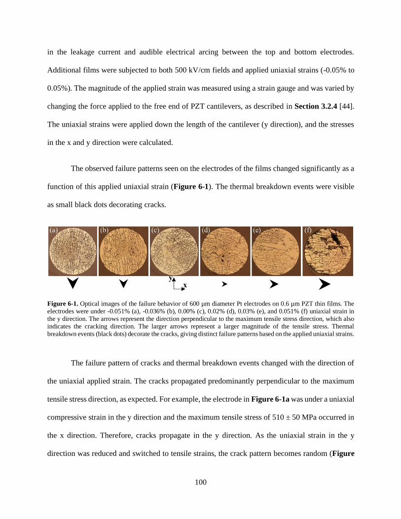
100
in the leakage current and audible electrical arcing between the top and bottom electrodes.
Additional films were subjected to both 500 kV/cm fields and applied uniaxial strains (-0.05% to
0.05%). The magnitude of the applied strain was measured using a strain gauge and was varied by
changing the force applied to the free end of PZT cantilevers, as described in Section 3.2.4 [44].
The uniaxial strains were applied down the length of the cantilever (y direction), and the stresses
in the x and y direction were calculated.
The observed failure patterns seen on the electrodes of the films changed significantly as a
function of this applied uniaxial strain (Figure 6-1). The thermal breakdown events were visible
as small black dots decorating cracks.
Figure 6-1. Optical images of the failure behavior of 600 µm diameter Pt electrodes on 0.6 µm PZT thin films. The
electrodes were under -0.051% (a), -0.036% (b), 0.00% (c), 0.02% (d), 0.03% (e), and 0.051% (f) uniaxial strain in
the y direction. The arrows represent the direction perpendicular to the maximum tensile stress direction, which also
indicates the cracking direction. The larger arrows represent a larger magnitude of the tensile stress. Thermal
breakdown events (black dots) decorate the cracks, giving distinct failure patterns based on the applied uniaxial strains.
The failure pattern of cracks and thermal breakdown events changed with the direction of
the uniaxial applied strain. The cracks propagated predominantly perpendicular to the maximum
tensile stress direction, as expected. For example, the electrode in Figure 6-1a was under a uniaxial
compressive strain in the y direction and the maximum tensile stress of 510 ± 50 MPa occurred in
the x direction. Therefore, cracks propagate in the y direction. As the uniaxial strain in the y
direction was reduced and switched to tensile strains, the crack pattern becomes random (Figure
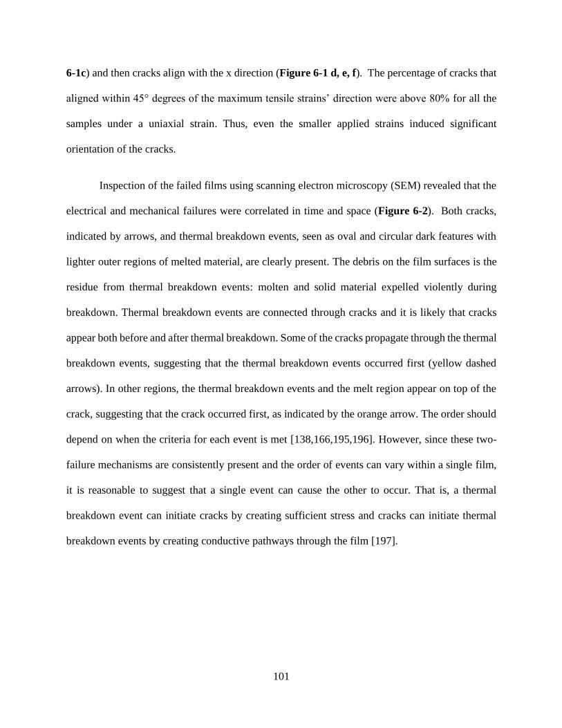
101
6-1c) and then cracks align with the x direction (Figure 6-1 d, e, f). The percentage of cracks that
aligned within 45° degrees of the maximum tensile strains’ direction were above 80% for all the
samples under a uniaxial strain. Thus, even the smaller applied strains induced significant
orientation of the cracks.
Inspection of the failed films using scanning electron microscopy (SEM) revealed that the
electrical and mechanical failures were correlated in time and space (Figure 6-2). Both cracks,
indicated by arrows, and thermal breakdown events, seen as oval and circular dark features with
lighter outer regions of melted material, are clearly present. The debris on the film surfaces is the
residue from thermal breakdown events: molten and solid material expelled violently during
breakdown. Thermal breakdown events are connected through cracks and it is likely that cracks
appear both before and after thermal breakdown. Some of the cracks propagate through the thermal
breakdown events, suggesting that the thermal breakdown events occurred first (yellow dashed
arrows). In other regions, the thermal breakdown events and the melt region appear on top of the
crack, suggesting that the crack occurred first, as indicated by the orange arrow. The order should
depend on when the criteria for each event is met [138,166,195,196]. However, since these two-
failure mechanisms are consistently present and the order of events can vary within a single film,
it is reasonable to suggest that a single event can cause the other to occur. That is, a thermal
breakdown event can initiate cracks by creating sufficient stress and cracks can initiate thermal
breakdown events by creating conductive pathways through the film [197].
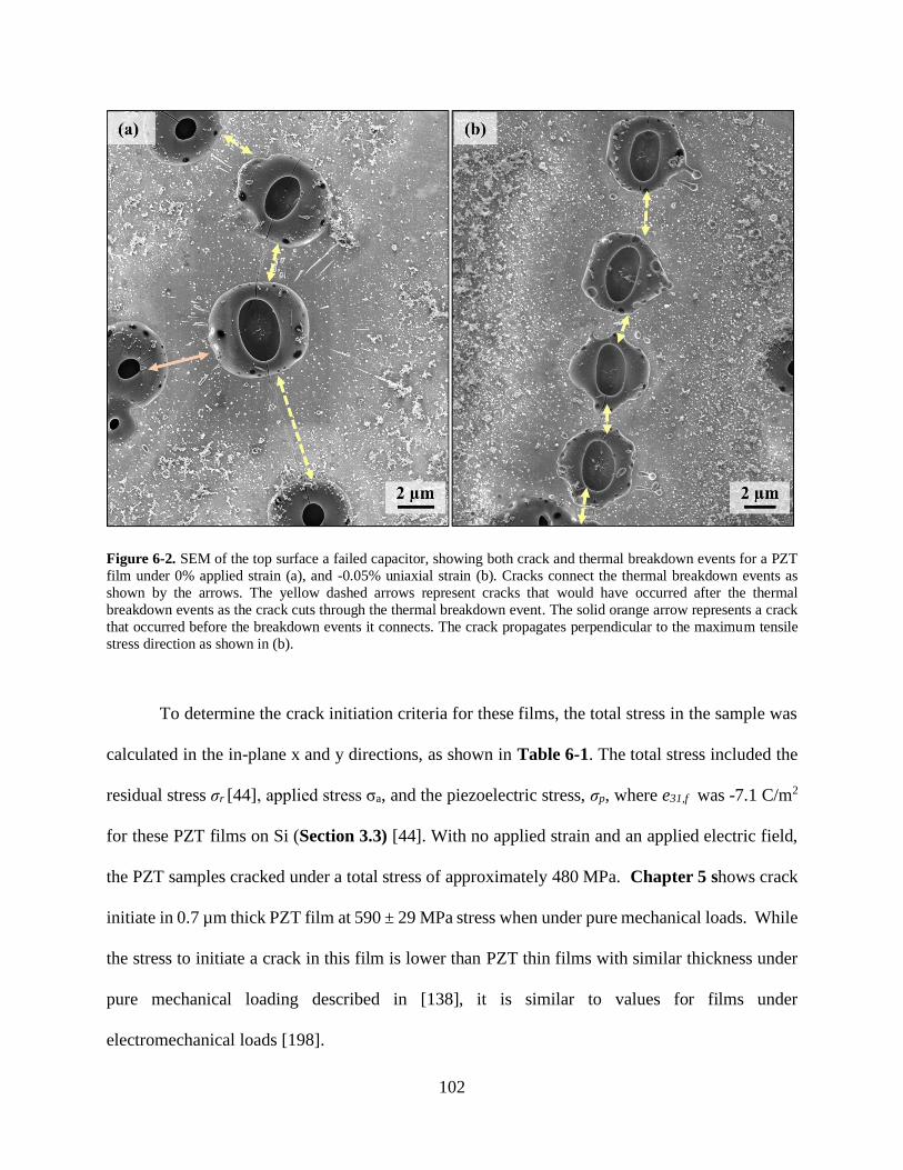
102
Figure 6-2. SEM of the top surface a failed capacitor, showing both crack and thermal breakdown events for a PZT
film under 0% applied strain (a), and -0.05% uniaxial strain (b). Cracks connect the thermal breakdown events as
shown by the arrows. The yellow dashed arrows represent cracks that would have occurred after the thermal
breakdown events as the crack cuts through the thermal breakdown event. The solid orange arrow represents a crack
that occurred before the breakdown events it connects. The crack propagates perpendicular to the maximum tensile
stress direction as shown in (b).
To determine the crack initiation criteria for these films, the total stress in the sample was
calculated in the in-plane x and y directions, as shown in Table 6-1. The total stress included the
residual stress σr [44], applied stress σa, and the piezoelectric stress, σp, where e31,f was -7.1 C/m2
for these PZT films on Si (Section 3.3) [44]. With no applied strain and an applied electric field,
the PZT samples cracked under a total stress of approximately 480 MPa. Chapter 5 shows crack
initiate in 0.7 µm thick PZT film at 590 ± 29 MPa stress when under pure mechanical loads. While
the stress to initiate a crack in this film is lower than PZT thin films with similar thickness under
pure mechanical loading described in [138], it is similar to values for films under
electromechanical loads [198].
103
Table 6-1. Calculated stresses in the x and y direction for films represented in Figure 6-2 a-f. For σp, the piezoelectric
coefficient, e31,f was estimated to be -7.1±0.35 C/m2. Numbers in bold indicate the maximum tensile stress for the
sample. To calculate the applied stress in the x (σa,x) direction the Poisson’s ratio of 0.3, and Young’s modulus of 90
GPa for (001) oriented PZT was used [93]. Values are in MPa unless otherwise noted.
Electrode σr σp σa,y σa,x σtot,y σtot,x
a 130 ± 30 350 ± 20 -45 14 455 514
b 130 ± 30 350 ± 20 -32 10 468 510
c 130 ± 30 350 ± 20 0 0 480 480
d 130 ± 30 350 ± 20 18 -5 518 495
e 130 ± 30 350 ± 20 27 -8 527 492
f 130 ± 30 350 ± 20 46 -14 546 485
The reduction in total stress required for crack initiation may be a result of several factors
and was investigated in Section 6.3. These factors include the piezoelectric stress, changes in the
local stresses with field, and a reduction in domain wall motion. Overall, this initial study reveals
that under electromechanical failure, there is a correlation between cracks and thermal breakdown
events and the failure pattern depends on the applied strain direction. Cracking would occur when
the total stress reaches the crack initiation stress of the film, which was reduced with applied
electric fields parallel to the remanent polarization direction.
6.3 Influence of Electrical History on Failure of Lead Zirconate Titanate Thin Films
This section aims to understand how the electrical history of the piezoelectric film
affects its performance by investigating property changes and changes in mechanical limits of
films with difference electrical histories (virgin, poled, and under DC bias). Dielectric and
piezoelectric properties of PZT thin films with various electrical conditions are measured in order
to quantify the figures of merit (FoM) for different applications based on the electrical history.
The FoMs used in this study are related to the piezoelectric coefficient (𝑒31,𝑓) and dielectric
104
constant (r) of the film; for actuators, the FoM is 𝑒31,𝑓 , for voltage-based sensors, FoM is 𝑒31,𝑓
𝑟,
and for energy harvesters, FoM is 𝑒31,𝑓
2
𝑟 [23–26]. This section employs Ball on three Ball (B3B)
testing on PZT films with various electrical history to quantify the effects of electric field on the
crack initiation stress and crack propagation in the PZT thin film and PZT/Si stacks. The results
are analyzed and compared with the response of similar PZT films under pure mechanical loading.
6.3.1 Experimental Details
6.3.1.1 Sample preparation and materials characterization
Niobium doped PZT (Pb0.99(Zr0.52Ti0.48)0.98Nb0.02O3) films were grown by chemical
solution deposition on a platinized 4-inch Si wafers (NOVA Electronic Materials) as described in
Section 3.2.1. A total of 20 layers (each layer thickness was ~80 nm) was deposited on the
substrate, which yielded a thickness of ~1.6 µm, as measured over an etch step using a contact
profilometer (KLA Tencor 16+). The stack has six layers: a 1.6 µm PZT layer, a 100 nm Pt bottom
electrode, a 20 nm Ti/TiO2 adhesion layer, 1 µm SiO2 layer, ~500 µm Si substrate, and a 1 µm
SiO2 layer. The structure of the stack is shown in Figure 6-3. The film’s crystallographic
orientation was determined using XRD with a PANalytical Empyrean diffractometer with a Cu
Kα X-Ray source. The grain size was determined using the line intercept method [199] on several
micrographs, taken with a FeSEM.
Pt top electrodes were deposited to a thickness of 100 nm using a Kurt Lesker CMS-18
sputter tool (Section 3.2.3). The design of the top electrode (shown in Figure 6-3, top right) covers
the center of the sample, with a 1 mm diameter circle and a contact pad to the side. This electrode
design allows for easy contact during mechanical loading and makes it possible to pole the center
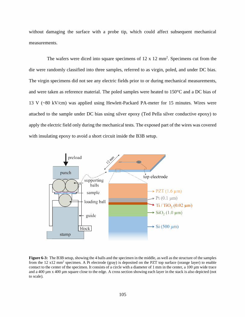
105
without damaging the surface with a probe tip, which could affect subsequent mechanical
measurements.
The wafers were diced into square specimens of 12 x 12 mm2. Specimens cut from the
die were randomly classified into three samples, referred to as virgin, poled, and under DC bias.
The virgin specimens did not see any electric fields prior to or during mechanical measurements,
and were taken as reference material. The poled samples were heated to 150°C and a DC bias of
13 V (~80 kV/cm) was applied using Hewlett-Packard PA-meter for 15 minutes. Wires were
attached to the sample under DC bias using silver epoxy (Ted Pella silver conductive epoxy) to
apply the electric field only during the mechanical tests. The exposed part of the wires was covered
with insulating epoxy to avoid a short circuit inside the B3B setup.
Figure 6-3: The B3B setup, showing the 4 balls and the specimen in the middle, as well as the structure of the samples
from the 12 x12 mm2 specimen. A Pt electrode (gray) is deposited on the PZT top surface (orange layer) to enable
contact to the center of the specimen. It consists of a circle with a diameter of 1 mm in the center, a 100 µm wide trace
and a 400 µm x 400 µm square close to the edge. A cross section showing each layer in the stack is also depicted (not
to scale).
106
6.3.1.2 Measurement of electrical properties
The film’s permittivity and loss were recorded as a function of frequency (100 Hz to 100
kHz) using a Hewlett Packard 4284A precision LCR meter with a small (30 mV) AC signal applied
to the bottom electrode. The polarization electrical field (P-E) hysteresis loop was measured at 100
Hz using a Radiant Precision Multiferroic Ferroelectric Tester [44]. Additionally, the Rayleigh
behavior of the permittivity was measured up to 35 kV/cm (~ ½ the coercive field, Ec, at 1 kHz).
The e31,f was measured using the wafer flexure method described by Wilke et al. [200]. All
experiments were conducted under ambient conditions (~20°C and ~40-60% RH), and a minimum
of three specimens per sample type was used for each measurement.
6.3.1.3 Electromechanical loading: Ball on three ball testing
The relationship between the electric fields and the structural limits of PZT thin films
was tested using the B3B biaxial bending test using plate-like test setup [172], as described in
Section 5.2.2. This leads to a well-defined biaxial stress field, with the highest tensile stresses
acting in the middle of the surface, opposite to the one loading ball [201]. Using the B3B set up,
the characteristic stack strength of the different samples (loading to failure) and the stress required
for crack initiation in the PZT layer (pre-loading and unloading for inspection) were determined.
The strength of the virgin, poled, and under DC bias samples was determined using a
minimum of 12 specimens (per sample) tested following the same procedure (preload of about 10
N and a displacement-controlled rate of 0.1 mm/min) using a universal tester (Instron, Ma). The
strength of the Pt/Ti/TiO2/SiO2/Si/SiO2 substrate was also measured for comparison. The poled
samples were all aged a minimum of 20 hours after poling. The samples under DC bias had 13 V
(~80 kV/cm) applied during the mechanical measurements and had no exposure to an electric field
prior to measurement. The DC field was applied using a Keysight E4980A precision LCR meter
107
and the permittivity was also measured during the mechanical testing using the same LCR meter
with a 30 mV 1 kHz signal superimposed on the DC bias. The strength of the stack was determined
introducing the fracture force, F, into Equation 5-4. For this work, since most of the stack
thickness is from the Si substrate, it is assumed σmax is the stress in the Si layer. The stresses in
each of the layers is calculated as described in Section 5.2.2 and the supplemental materials in
[138].
In order to determine the crack initiation stress, an additional set of five specimens of
each sample with distinct electrical history was loaded between 20-70% of the corresponding
characteristic load using the B3B setup (see Section 5.2.2). The pre-cracks initiated during the
loading process were identified using an optical microscope in dark field mode. The force at which
cracks were first observed was recorded as the applied force for cracking.
6.3.2 Results and Discussion
6.3.2.1 Structural Characterization
Figure 6-4a shows the microstructure of the PZT layer, with an average lateral grain size
of 126 ± 54 nm. Figure 6-4b shows the cross section of the sample, in which individually deposited
layers can be identified; a small amount of pyrochlore or fluorite grains is apparent at individual
crystallization interfaces. The thickness of the PZT films was ~1.6 µm. Figure 6-5 shows the XRD
patterns corresponding to the PZT layer. The film had an approximately random orientation.

108
Figure 6-4: (a) Top view SEM image showing the grain size of the PZT layer. (b) Cross sectional SEM image showing
the layered structure of the 1.6 µm thick PZT layer, as well as the platinum bottom electrode.
Figure 6-5: XRD pattern of the PZT layer, showing random orientation. The symbol “*” indicates background peaks
from the substrate.
6.3.2.2 Electrical Characterization
At 1 kHz under low oscillating electric fields (18.75 V/cm), r was 1100 ± 24, 1073 ± 16,
and 740 ± 16 for the virgin, poled, and under DC bias samples, respectively. As the frequency

109
increased, r decreased slightly for all samples. The relative permittivity was also measured as a
function of increasing AC field (Figure 6-6). In this low field regime, a linear Rayleigh-like regime
was identified using Equation 2-11. The irreversible Rayleigh parameter, αray, captures the
irreversible domain wall motion contribution and εinit includes both the reversible domain wall
motion and intrinsic contributions to the permittivity. A linear Rayleigh regime for all samples was
fitted between 7 and 23 kV/cm (~10-50% of Ec) with R2 of 0.994 or greater. In the Rayleigh
regime, εinit was 1099 ± 17, 1059 ± 17, 735 ± 17 for the virgin, poled, and film under DC bias,
respectively. α was 22 ± 2, 15.75 ± 1.25, 5.5 ± 0.14 cm/kV for the virgin, poled, and film under
DC bias, respectively.
Figure 6-6: Relative permittivity as a function of AC signal for the virgin (green upward triangle), poled (red square),
and under DC bias (orange downward triangle) films. The linear Rayleigh regime is denoted between the two vertical
dashed lines and was consistent for all the films.
The low εinit for the sample under DC bias is due to dielectric stiffening. The difference
between εinit for the virgin and poled sample was modest, suggesting that there is a limited
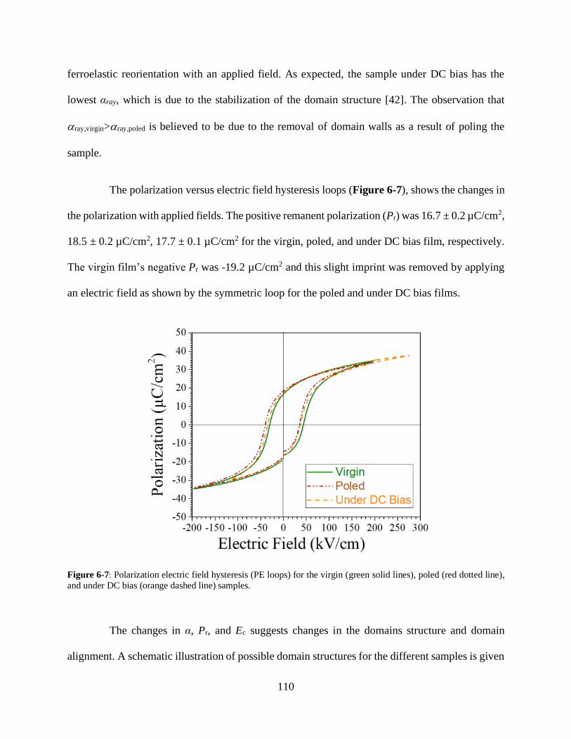
110
ferroelastic reorientation with an applied field. As expected, the sample under DC bias has the
lowest αray, which is due to the stabilization of the domain structure [42]. The observation that
ray,virgin>ray,poled is believed to be due to the removal of domain walls as a result of poling the
sample.
The polarization versus electric field hysteresis loops (Figure 6-7), shows the changes in
the polarization with applied fields. The positive remanent polarization (Pr) was 16.7 ± 0.2 µC/cm2,
18.5 ± 0.2 µC/cm2, 17.7 ± 0.1 µC/cm2 for the virgin, poled, and under DC bias film, respectively.
The virgin film’s negative Pr was -19.2 µC/cm2 and this slight imprint was removed by applying
an electric field as shown by the symmetric loop for the poled and under DC bias films.
Figure 6-7: Polarization electric field hysteresis (PE loops) for the virgin (green solid lines), poled (red dotted line),
and under DC bias (orange dashed line) samples.
The changes in α, Pr, and Ec suggests changes in the domains structure and domain
alignment. A schematic illustration of possible domain structures for the different samples is given

111
in Figure 6-8. As indicated by the largest Pr, the poled sample should have more domains aligned
with the applied electric field compared to the virgin sample. The sample under DC bias is also
expected to have more domains aligned and fewer domain walls than the virgin sample. However,
this alignment is incomplete since the film under DC bias is only under electric field during the
measurement.
Figure 6-8: Schematic illustration of the domain structure for the virgin (green), poled (red) and under DC bias
(orange) sample. Arrows represent the polarization direction for the respective domains.
Due to the differences in domain structure, the films have different piezoelectric
coefficients and FoM. The various FoM are shown in Table 6-2. Table of the calculated figure of merits
(FoM) for the various applications for sensors, actuators and energy harvesting devices.Table 6-2, where the
piezoelectric coefficient, e31,f, was measured to be 0 C/m2, -6.5 ± 0.6 C/m2 and -4.1 ± 0.3 C/m2 for
the virgin, poled, and under DC bias sample, respectively. The poled sample has the largest
coefficient, presumably because the sample under DC bias was only partially poled. The poled
sample also had the highest FoM for all applications compared to the virgin and the sample under
a DC bias. An additional sample that was poled, aged for 24 hrs., and then measured under a DC
bias is also reported in Table 6-2. The piezoelectric coefficient was slightly lower than the poled
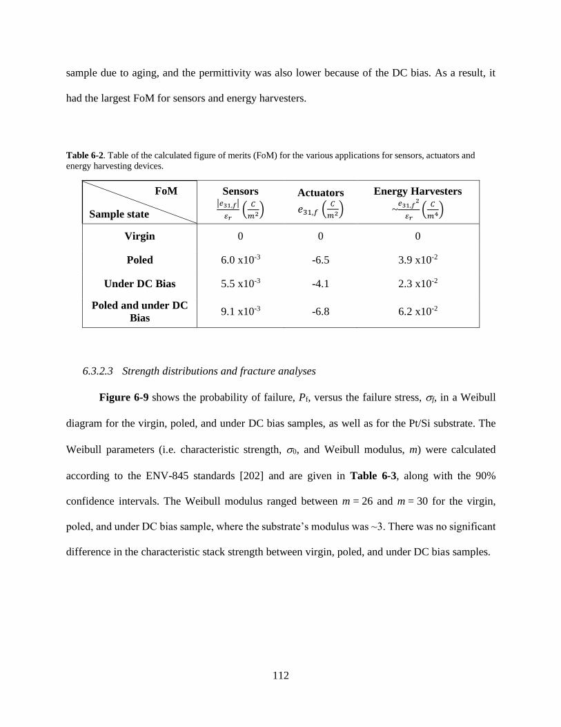
112
sample due to aging, and the permittivity was also lower because of the DC bias. As a result, it
had the largest FoM for sensors and energy harvesters.
Table 6-2. Table of the calculated figure of merits (FoM) for the various applications for sensors, actuators and
energy harvesting devices.
FoM
Sample state
Sensors |𝑒31,𝑓|
𝑟 (
𝐶
𝑚2)
Actuators
𝑒31,𝑓 (𝐶
𝑚2)
Energy Harvesters
~𝑒31,𝑓
2
𝑟(
𝐶
𝑚4)
Virgin 0 0 0
Poled 6.0 x10⁻³ -6.5 3.9 x10⁻²
Under DC Bias 5.5 x10⁻³ -4.1 2.3 x10⁻²
Poled and under DC
Bias 9.1 x10⁻³ -6.8 6.2 x10⁻²
6.3.2.3 Strength distributions and fracture analyses
Figure 6-9 shows the probability of failure, Pf, versus the failure stress, f, in a Weibull
diagram for the virgin, poled, and under DC bias samples, as well as for the Pt/Si substrate. The
Weibull parameters (i.e. characteristic strength, 0, and Weibull modulus, m) were calculated
according to the ENV-845 standards [202] and are given in Table 6-3, along with the 90%
confidence intervals. The Weibull modulus ranged between m = 26 and m = 30 for the virgin,
poled, and under DC bias sample, where the substrate’s modulus was ~3. There was no significant
difference in the characteristic stack strength between virgin, poled, and under DC bias samples.
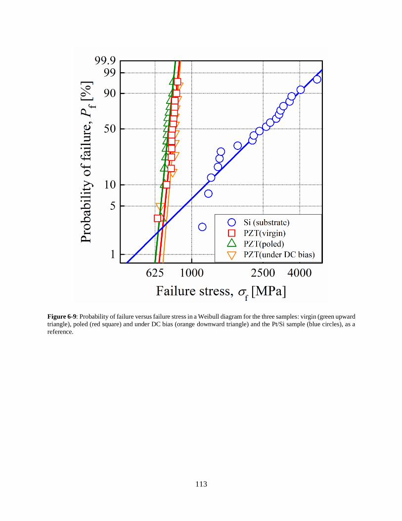
113
Figure 6-9: Probability of failure versus failure stress in a Weibull diagram for the three samples: virgin (green upward
triangle), poled (red square) and under DC bias (orange downward triangle) and the Pt/Si sample (blue circles), as a
reference.
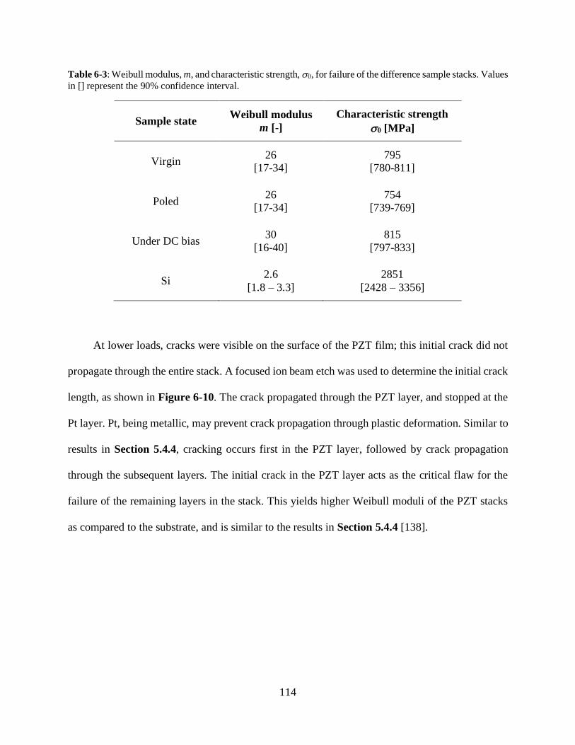
114
Table 6-3: Weibull modulus, m, and characteristic strength, 0, for failure of the difference sample stacks. Values
in [] represent the 90% confidence interval.
Sample state Weibull modulus
m [-]
Characteristic strength
0 [MPa]
Virgin 26
[17-34]
795
[780-811]
Poled 26
[17-34]
754
[739-769]
Under DC bias 30
[16-40]
815
[797-833]
Si 2.6
[1.8 – 3.3]
2851
[2428 – 3356]
At lower loads, cracks were visible on the surface of the PZT film; this initial crack did not
propagate through the entire stack. A focused ion beam etch was used to determine the initial crack
length, as shown in Figure 6-10. The crack propagated through the PZT layer, and stopped at the
Pt layer. Pt, being metallic, may prevent crack propagation through plastic deformation. Similar to
results in Section 5.4.4, cracking occurs first in the PZT layer, followed by crack propagation
through the subsequent layers. The initial crack in the PZT layer acts as the critical flaw for the
failure of the remaining layers in the stack. This yields higher Weibull moduli of the PZT stacks
as compared to the substrate, and is similar to the results in Section 5.4.4 [138].
115
Figure 6-10: FIB image showing the crack stop at the interface of the PZT and Pt seed layer beneath. The image was
prepared using a FEI Scios Focused Ion Beam (FIB) system. The porosity in the SiO2 layer may be due to lead
diffusion through the stack, and some damage from the FIB.
The stress to initiate a crack in the PZT layer depended on the electrical history as shown
in Table 6-4. The virgin sample had cracks initiate at stresses around 500 MPa. Although the film
has a random orientation and some pyrochlore present, this stress to initiate a crack is similar to
the predicted crack initiation stress range for PZT films with similar thicknesses (1.8 µm) reported
in Section 5.3.3 [138,147]. However, crack initiation occurred at lower stresses for both the poled
sample, and the sample measured under DC bias (around 400 MPa). Initially, this difference was
attributed to inaccuracies in the calculated piezoelectric stress. It was assumed that the e31,f did not
change with applied mechanical load or time, but other reports suggest that the piezoelectric
coefficient will change with both field and stress [44,100]. However, this does not account for the
decrease in crack initiation stress for the poled sample, since it was not under an applied electric
field during B3B loading and there is a statistically significant decrease in the crack initiation stress
compared to the virgin sample.
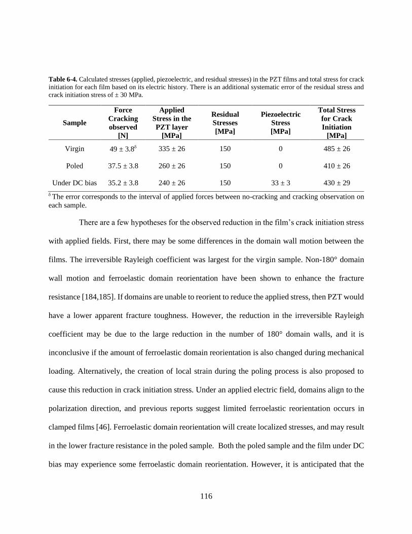
116
Table 6-4. Calculated stresses (applied, piezoelectric, and residual stresses) in the PZT films and total stress for crack
initiation for each film based on its electric history. There is an additional systematic error of the residual stress and
crack initiation stress of ± 30 MPa.
Sample
Force
Cracking
observed
[N]
Applied
Stress in the
PZT layer
[MPa]
Residual
Stresses
[MPa]
Piezoelectric
Stress
[MPa]
Total Stress
for Crack
Initiation
[MPa]
Virgin 49 ± 3.8 335 ± 26 150 0 485 ± 26
Poled 37.5 ± 3.8 260 ± 26 150 0 410 ± 26
Under DC bias 35.2 ± 3.8 240 ± 26 150 33 ± 3 430 ± 29
The error corresponds to the interval of applied forces between no-cracking and cracking observation on
each sample.
There are a few hypotheses for the observed reduction in the film’s crack initiation stress
with applied fields. First, there may be some differences in the domain wall motion between the
films. The irreversible Rayleigh coefficient was largest for the virgin sample. Non-180° domain
wall motion and ferroelastic domain reorientation have been shown to enhance the fracture
resistance [184,185]. If domains are unable to reorient to reduce the applied stress, then PZT would
have a lower apparent fracture toughness. However, the reduction in the irreversible Rayleigh
coefficient may be due to the large reduction in the number of 180° domain walls, and it is
inconclusive if the amount of ferroelastic domain reorientation is also changed during mechanical
loading. Alternatively, the creation of local strain during the poling process is also proposed to
cause this reduction in crack initiation stress. Under an applied electric field, domains align to the
polarization direction, and previous reports suggest limited ferroelastic reorientation occurs in
clamped films [46]. Ferroelastic domain reorientation will create localized stresses, and may result
in the lower fracture resistance in the poled sample. Both the poled sample and the film under DC
bias may experience some ferroelastic domain reorientation. However, it is anticipated that the
117
poled film may have more domain alignment and may also have slightly more local strains from
ferroelastic switching. The extent of ferroelastic domain reorientation is not measured in this study
and therefore future work should explore the mechanism governing this trend. Overall, this study
suggests that poling and electric fields can reduce the crack initiation stress up to 15% and confirms
the failure observation in Section 6.2.
6.4 In situ property measurements under electromechanical loads
To further explore the relationship between electromechanical loading and the changes
in properties, PZT films under DC bias had their relative permittivity and loss tangent recorded
during the B3B loading experiment (Figure 6-11). The plots are segmented into three regions (I,
II, and III). Region I is the preload region, where the PZT sample is loaded up to 10 N prior to the
start of the experiment. Region II begins when the DC bias of 80 kV/cm is applied, the permittivity
is recorded, and a downward force on the mechanical fixture is applied at a rate of 0.1 mm/s.
During this stage, cracks were not observed on the film’s surface, since the stresses are lower than
the reported crack initiation stress. Region III corresponds to the forces at which surface cracks
are observed.
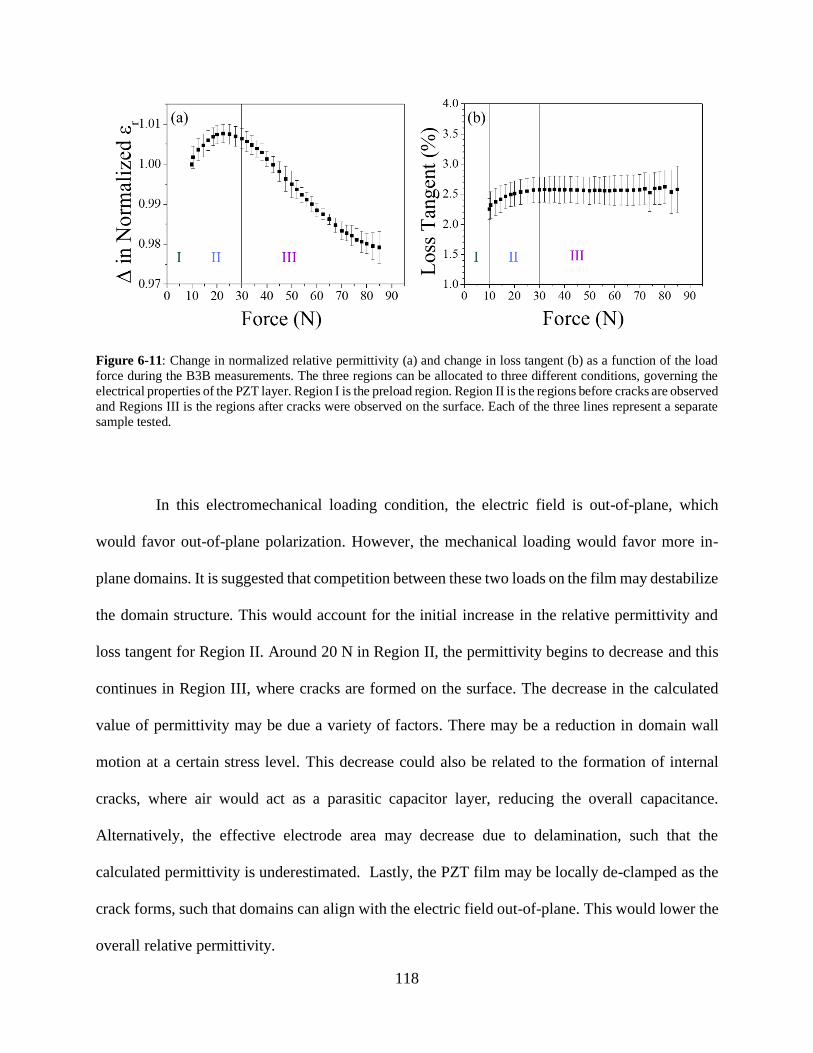
118
Figure 6-11: Change in normalized relative permittivity (a) and change in loss tangent (b) as a function of the load
force during the B3B measurements. The three regions can be allocated to three different conditions, governing the
electrical properties of the PZT layer. Region I is the preload region. Region II is the regions before cracks are observed
and Regions III is the regions after cracks were observed on the surface. Each of the three lines represent a separate
sample tested.
In this electromechanical loading condition, the electric field is out-of-plane, which
would favor out-of-plane polarization. However, the mechanical loading would favor more in-
plane domains. It is suggested that competition between these two loads on the film may destabilize
the domain structure. This would account for the initial increase in the relative permittivity and
loss tangent for Region II. Around 20 N in Region II, the permittivity begins to decrease and this
continues in Region III, where cracks are formed on the surface. The decrease in the calculated
value of permittivity may be due a variety of factors. There may be a reduction in domain wall
motion at a certain stress level. This decrease could also be related to the formation of internal
cracks, where air would act as a parasitic capacitor layer, reducing the overall capacitance.
Alternatively, the effective electrode area may decrease due to delamination, such that the
calculated permittivity is underestimated. Lastly, the PZT film may be locally de-clamped as the
crack forms, such that domains can align with the electric field out-of-plane. This would lower the
overall relative permittivity.
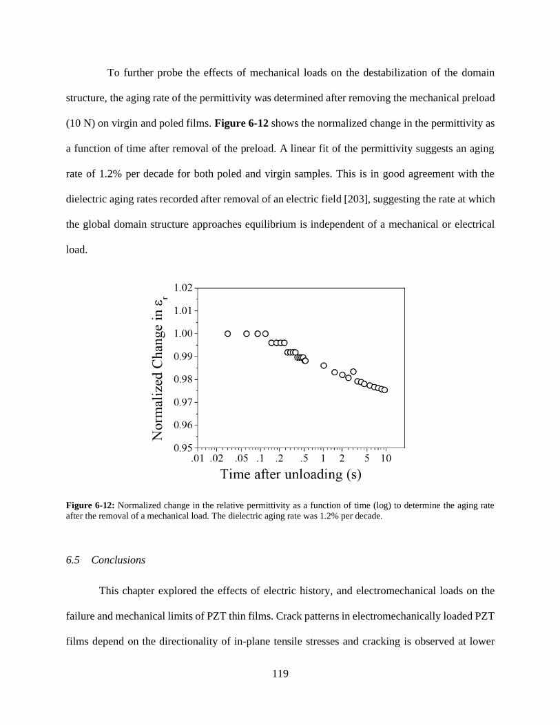
119
To further probe the effects of mechanical loads on the destabilization of the domain
structure, the aging rate of the permittivity was determined after removing the mechanical preload
(10 N) on virgin and poled films. Figure 6-12 shows the normalized change in the permittivity as
a function of time after removal of the preload. A linear fit of the permittivity suggests an aging
rate of 1.2% per decade for both poled and virgin samples. This is in good agreement with the
dielectric aging rates recorded after removal of an electric field [203], suggesting the rate at which
the global domain structure approaches equilibrium is independent of a mechanical or electrical
load.
Figure 6-12: Normalized change in the relative permittivity as a function of time (log) to determine the aging rate
after the removal of a mechanical load. The dielectric aging rate was 1.2% per decade.
6.5 Conclusions
This chapter explored the effects of electric history, and electromechanical loads on the
failure and mechanical limits of PZT thin films. Crack patterns in electromechanically loaded PZT
films depend on the directionality of in-plane tensile stresses and cracking is observed at lower
120
loads than virgin films made on the same wafer. Failure under electromechanical loading
conditions was observed as a combination of thermal breakdown events and cracks in films
clamped to a Si substrate. Additionally, the electric history of the sample dictates the performance
of the films, influences the FoM, and may reduce the crack initiation stress. While poling enhances
the piezoelectric response of the film, it reduces the stress that the films can withstand during
operation, prior to cracking. While this reduction may be due to a series of factors, this observation
was noted for a series of films under different loading conditions. Lastly, the application of
electromechanical loads may destabilize the domain structure and the removal of mechanical loads
leads to similar dielectric aging rates that are reported after the removal of electrical loads. This
suggests that the time for the domain structure to reach a new equilibrium position is independent
of the type of load. This chapter emphasizes the necessity to quantify the mechanical loads on
piezoelectric films, as they may destabilize the domain structure, and in electromechanical
applications, failure may ensue at lower loads than predicted from mechanical-only testing.

121
Chapter 7. Conclusions and Future Work
7.1 Conclusions
This thesis discusses the influence of mechanical stresses (applied, residual, and
piezoelectrically-induced) on the dielectric and piezoelectric properties of PZT thin films. The
limits of stress that PZT films could tolerate was found to be a function of film thickness, electrical
history, and loading conditions. In particular, thicker films tend to have lower mechanical limits
compared to thinner films, and the electric history and the substrate can play a critical role in the
applied stress limits of the film. Additionally, compressive stresses were shown to improve
piezoelectric properties, increase applied stress limits before failure, and increase the number of
out-of-plane domains. Tailoring the residual stress in thin films can tune dielectric and
piezoelectric properties, reduce the propensity for cracking, and improve their performance in
various piezoMEMS applications.
The effect of total stress on the dielectric and piezoelectric properties of PZT films grown
on Ni and Si foils was investigated (Chapter 3). PZT films grown on Ni foil experience
compressive residual stresses and had larger piezoelectric coefficients (e31,f = –9.7 ± 0.45 C/m2)
and remanent polarizations (Pr = 39.5 ± 2.3 µC/cm2) compared to PZT films grown on Si wafers
(e31,f = –7 ± 0.35 C/m2, Pr = 21 ± 0.2 µC/cm2). Due to tensile residual stress, PZT on Si had a larger
relative permittivity (εr = 1040 ± 20) than PZT on Ni (εr = 600 ± 80). With additional compressive
strains applied to films on either substrate, the remanent polarization and piezoelectric properties
increased and the relative permittivity decreased. The opposite occurred under tensile stress,
suggesting some ferroelastic domain reorientation could occur in these films. Property changes
were approximately linear with stress changes; the slope differed between the two substrates. The
slope of the remanent polarization versus stress was -0.013 MPa/(µC/cm2) and -0.021

122
MPa/(µC/cm2) for PZT on Ni and Si, respectively. Within the stress limits, the properties of PZT
on Ni and Si did not overlap, indicating that residual stress and the resulting domain structure
dictate the range and tunability of both dielectric and piezoelectric properties.
To further probe the relationship between the changes in the properties with stresses in the
film, Chapter 4 revealed differences in the intrinsic and extrinsic contributions to the dielectric
and pyroelectric properties. PZT on Ni is under 530 MPa of compressive residual stress and PZT
on Si is under 130 MPa of tensile residual stress. The magnitude of residual stress significantly
influenced the extrinsic contributions to film properties. Both the Rayleigh and Preisach responses
show a large reduction in irreversible property contributions for PZT films on Ni as the temperature
decreased towards 0 K. At room temperature, αray was 15.5 ± 0.1 cm/kV and 28.4 ± 1.6 cm/kV for
PZT on Si and Ni, respectively and the large amount of irreversible domain wall motion for PZT
on Ni may be due to the flexibility of Ni foil. However, as thermal energy decreased, domain wall
motion decreased at a higher rate for PZT on Ni, which may be due to a combination of increased
residual stress at lower temperatures and decreased thermal energy. PZT films on Si did not show
large changes in residual stress in the films when cooled to 10 K and had a smaller reduction in
the irreversible Rayleigh coefficient. This is because PZT and Si have very similar thermal
expansion coefficients at lower temperatures. It is believed that these results can be explained by
a narrower distribution of pinning potentials for PZT on Ni relative to PZT on Si. Overall, the
residual stresses and substrate choice influence the domain structure and the pinning centers
causing some films to have less domain wall motion.
Stress limits in PZT thin films were investigated (Chapter 5). First, crack initiation stress
was studied as a function of film thickness. Thicker films required lower stresses for crack
initiation, where 0.7 µm PZT films required stresses around 590 MPa, and 1.8 µm films required
123
stresses around 490 MPa to initiate a crack. The literature previously attributed this to either
changes in the residual stresses of thick films, or the Weibullian volume effect. This work suggests
that instead, the coupled stress-energy criterion for crack initiation affects the mechanical limits of
these films. This depends on the thickness of the films, where thinner films require a higher load
to reach their energy criteria and fail. The slight deviation between the model and experimental
observation may be due to differences in domain wall mobility. Thinner films tend to have less
domain wall motion and thus, a lower fracture toughness. The current model only considers one
value for the fracture toughness as the fracture toughness for PZT thin films has yet to be
determined.
This biaxial ball-on-three-ball test method was also used to explore how cracks initiated
and propagated through the entire stack. PZT/LaNiO3/SiO2/Si stack failure occurred in two stages.
First, the PZT layer cracked; the crack then arrested at the SiO2 layer due to the significant
compressive stress in the SiO2. With a higher applied stress, the crack propagated through the
remainder of the stack. As shown by the Griffith-Irwin crack resistance model, stacks with thinner
PZT films require higher stresses for failure because the initial crack length is shorter. It was also
found that the Weibull modulus was significantly larger for PZT on Si (m ≥ 10) compared to the
Si substrate itself (m = 3). This occurred because the stack had a consistent pre-crack length
corresponding to the PZT film’s thickness. To design stacks with increased strength, thin layers
under compressive stress should be considered.
In addition to pure mechanical failure, it was found that electromechanical loading could
also affect the PZT layer’s mechanical limits in Chapter 6. This occurs because the applied electric
field creates piezoelectric stress in the films; this can be large in films with high piezoelectric
responses and high breakdown strengths. Additionally, the electric field history of the sample may

124
affect the domain structure, domain wall mobility, and fracture toughness. These results
demonstrate a decrease in crack initiation stress in poled films or films under a DC bias. Poled
films had the lowest crack initiation stress possibly due to a reduced number of domain walls, and
creation of localized stress due to some ferroelastic reorientation; both of these factors would
reduce the fracture toughness. Both PZT films that were pre-poled and those under a DC bias
during mechanical testing showed larger piezoelectric properties, and required less stress to initiate
a crack.
Additionally, the orientation of applied stress and electrical load of PZT films was studied.
It was found that failure patterns depended on loading conditions. PZT films on Si wafers typically
failed electromechanically, where thermal breakdown appeared along cracks. These cracks
propagated perpendicular to the maximum tensile stress direction. The order in which failure
events occurred depended on whether the electrical or mechanical failure criterion was met first.
It is believed the presence of one failure facilitates subsequent failure events, as indicated by the
numerous correlated cracks and thermal breakdown events.
In the course of this thesis, stresses in PZT thin films were shown to affect the domain wall
motion, as well as the dielectric and piezoelectric properties. The influences of stress on the
performance of PZT thin films indicate that stresses can be used to tailor properties and improve
the functionality. In particular, compressive stresses enhance the piezoelectric coefficient. In
addition, compressive residual stress should also increase the applied stress limits of these brittle
films. Ultimately stresses may be used to improve the functionality of PZT thin films and proper
stress management can also ensure high structural integrity. Both of these will improve the
performance of PZT thin films for various piezoMEMS applications.

125
7.2 Future Work
This section explores several avenues of future research that would further quantify the
relationships between stress and the domain orientation, properties, and failure limits of PZT thin
films and other brittle, layered materials. Section 7.2.1 describes possible material characterization
techniques that could be used to determine structural changes in PZT films under stress. Section
7.2.2 proposes a method to determine the fracture toughness and strength of PZT films. Section
7.2.3 suggests techniques to quantify the oxygen vacancy concentrations [Voꞏꞏ] for PZT films on
Ni and Si, which also may affect trends found in this thesis. Section 7.2.4 explores the effect of
strain on the aging rates of dielectric and piezoelectric properties to determine if certain strains can
further stabilize the poled domain structure. This chapter ends in Section 7.2.5 with a discussion
of the procedures utilized in this work and their potential application to other material systems.
7.2.1 Structural characterization of films under strain
To complement the electrical characterization in Chapter 3, structural characterization of
domain orientation as a function of applied strain can be used to further validate the hypothesis
that some ferroelastic domain reorientation occurs in PZT films under strain. In particular, it would
be useful to be able to determine the coercive stresses in PZT films as a function of Zr/Ti ratio,
grain size, thickness, and residual stress state. It is proposed here that Raman analysis or X-Ray
Diffraction (XRD) can be used to distinguish these differences.
Raman analysis has previously been used to understand the phase assemblages in PZT and
quantify changes in stress and domain structures in piezoelectric thin films [98,204–211]. The
Raman peaks of the A1(TO1), A1(TO2), A1(TO3) and E(LO3) modes depend on stress and domain
orientation, i.e. the percentage of the “c” domains, in PZT thin films [98,210,211]. For example,
the E(LO3) mode intensity has been shown to increase when the percentage of “c” domains
126
decrease in PZT [98,210]. An increase in relative peak intensity with increasing tensile strain
would thus confirm a decrease in “c” domains with applied tensile strain.
In an initial study to assess the viability of using Raman to determine domain reorientation,
0.6 µm PZT films on Ni foil substrates were subjected to different applied strains using the radius
of curvature method (Section 3.2.4). Raman data were collected using a Horiba Scientific Labram
HR Evolution Raman Spectrometer; a 633 nm wavelength laser with 0.9 numerical aperture and
1.5 mW power was used. In addition, Raman data were acquired for samples of Ni with only HfO2
and LaNiO3 (LNO) films to determine which Raman peaks corresponded to the underlying layers.
At each applied stress state, 15 spots were scanned for a minimum of 6 minutes each.
The Raman data between 0 and 1000 cm-1 (Figure 7-1) show a number of broad
peaks from different PZT and LNO modes, as detailed in
Table 7-1 [205,212]. The broad peak 6, from 700 to 730 cm-1, corresponds to both the
E(LO3) and A1(LO3) modes [98]. To fit this peak, two Gaussian profiles at 700 and 733 cm-1 were
used. To compare the changes in intensity with strain, the relative intensity of this peak was
determined by dividing by a well-defined second peak that is ideally independent of stress and the
PZT layer. To confirm the trend, the relative intensity of peak 6 should be normalized to multiple
peaks, or the background.
Initially in this spectrum, the relative intensity of peak 6 was normalized using peak 4
because of its sharpness. Peak 4, which corresponded with the LNO Eg mode [212], was fitted at
400 cm-1 with a Gaussian profile. While 𝐼𝑝𝑒𝑎𝑘 6
𝐼𝑝𝑒𝑎𝑘 4 increased linearly under tensile stress [212] (Figure
7-1b), the LNO layer may also have changed with strain. Therefore, the Raman spectra of stacks
of the underlying layers (LNO/HfO2/Ni) under the same applied strain were subtracted from the
equivalent PZT/LNO/Ni spectra in order to remove the LNO peak. Unfortunately, after completing
127
this additional analysis, no clear trend between 𝐼𝑝𝑒𝑎𝑘 6 and tensile strain was detected. This could
suggest that the LNO mode changes with strain and convolutes the trend found in Figure 7-1b.
Overall, no conclusive trend can be drawn from these initial results.
In future work, modified Raman analysis may be used to quantify the domain state changes
in PZT. Removing the LNO layer to reduce overlap with lower intensity PZT peaks at lower
Raman shifts will improve the results as has been widely reported in the literature [98,210,211].
The use of Pt bottom electrodes on Ni foil would ensure that no peaks from the underlying layers
are in the spectrum. Polarized Raman should also be used to help decouple PZT modes that have
similar Raman shifts with strain [98,207,209]. Additionally, the use of PZT films with larger grain
size and narrower Raman peaks would improve peak fitting.
128
Figure 7-1. a) Raman spectra on Ni foil under different strain levels. The inset shows changes in 𝐼𝑝𝑒𝑎𝑘 6
𝐼𝑝𝑒𝑎𝑘 4 as a
function of applied strain level (b) Peak 4 corresponds to the 400 cm-1 Eg LNO peak. Peak 6 corresponds with the
E(LO3) and the A1(LO3) PZT mode, which is dependent on the domain structure and the relative intensity
decreases with a higher number of “c” domains.
Table 7-1. List of the PZT and LNO modes corresponding to the peaks in Figure 7-1 [205,212].
Peak Frequency (cm-1) PZT Modes LNO Modes
1 140-180 A1(TO1) Eg (at 150 cm-1)
2 ~180-230 E(TO2) A1g (at 220 cm-1)
3 ~230-350 B1, E(TO)4 --
4 ~350-420 -- Eg
5 ~470-640 E(TO3), ELO3, ETO3,
A1TO3, A1TO3 --
6 ~650-800 E(LO3) and A1(LO3) --

129
XRD could also be used to distinguish the changes in the domain structure with strain.
Several studies have shown that the 001 and 002 peak intensities increase, while the 100 and 200
peak intensities decreases in tetragonal PZT thin films with an applied out-of-plane
[46,70,213,214] electric field. Here, a similar study is proposed as a function of strain. While the
data would be hard to collect on MPB films, due to the strong smearing between peaks, it is
suggested that more interpretable data could be obtained with tetragonal compositions. Since
ferroelastic reorientation may be limited for clamped films [46,215,216], films on more flexible
substrates, like Ni foil, which show higher irreversible Rayleigh coefficients at room temperature
and can achieve higher strains, should be used. Additional experiments combining electric fields
and temperature sweeps with applied strain may further probe the energy barriers that reduce
domain reorientation in thin films.
7.2.2 Determine the fracture toughness of PZT thin films
The PZT film’s strength and fracture toughness (KIC) influence the crack initiation stresses.
In this thesis, bulk PZT KIc values were used in the finite fracture mechanics model [166] (Chapter
5) since data are not available for films. However, in PZT, the fracture toughness has been shown
to vary with domain wall motion [182–185]. Since PZT films are clamped to the substrate and
have limited domain wall motion [43,146], the lower reported fracture toughness values were used
in the models of this thesis. However, it is likely that the fracture toughness is not constant. Instead,
it is proposed that fracture toughness may change with film thickness, with thinner films having
lower fracture toughness, due to reductions in ferroelastic wall mobility in thinner films.
To determine the fracture toughness of PZT thin films, a novel micromachined cantilever
experiment is proposed [167,217–219]. In previous work on single crystal tungsten and CrN

130
coatings, micromachined cantilevers were etched using a focused ion beam [217–219]. A notch
was etched into these beams and KIc was determined using Equation 7-1, where σf is the fracture
stress, a is the notch depth, f is a shape factor, and t is the thickness [219].
𝐾𝐼𝑐 = 𝜎𝐹√𝜋𝑎𝑓 (𝑎
𝑡) (7-1)
For PZT films, σf is not well known but can be determined from un-notched micromachined
cantilevers by using Equation 7-2, where l is the length from the fixed cantilever end to the applied
force, F, and B is the cantilever’s width [219].
𝜎𝐹 = 6𝐹𝑙
𝐵𝑡2 (7-2)
In these studies, the cantilevers were made with focused ion beam etching; however this process
is serial, and so limits generation of a statically significant set of data [218]. Thus, in order to
increase the number of samples that may be tested, an array of PZT cantilevers can be fabricated
through conventional microfabrication processes. For this purpose, PZT films should be grown on
a Si wafer to various thicknesses in order to determine if the thickness of the film affects the PZT
film’s KIc. Then, the PZT, LNO, and SiO2 layers can be etched with CF4, Cl2, and Ar gas via a
ULVAC plasma etching tool. Then the Si substrate would be etched in the Si deep reactive ion
etch (DRIE) chamber using the Bosch method [220]. Finally, an isotropic etch of the Si using XeF2
[221] would finish the process. These etching steps are shown schematically in Figure 7-2.
131
Figure 7-2. A schematic of the proposed nanofabrication of a series of released PZT thin film beams. (a) shows a
schematic cross section of the as grown PZT layer (purple) on the LNO layer (green), on SiO2 (yellow) and Si (gray)
and a top view. (b) shows the first etches to create pits down through the Si layer. (c) shows the undercut of the Si
layer which would release the PZT cantilever beams. The top view has white tick marks to represent the region that
has been released.
Once the cantilevers are released, they can be tested in the micromachine nanoindenter (e.g.
at the University of Leoben) to determine the film’s strength and fracture toughness. A focused
ion beam would then etch a notch on the cantilevers. The notch on the sample would act as a flaw
of known size, such that when the sample breaks, the fracture toughness can be determined using
Equation 7-1. Unnotched samples would be used to determine the material’s strength.
Figure 7-3 shows a SEM cross section of an initial attempt to make PZT cantilevers.
Unfortunately, process flaws precluded interpretable measurements during the course of this
thesis. In particular, plasma etching damaged the PZT layer along the sidewall, exposing the
132
underlying SiO2 layer (marked as “SiO2 ledge”). Breaking these cantilevers with a nanoindenter
did not accurately determine the fracture toughness. Future work should explore ways to create
PZT cantilevers where the PZT edge is not damaged and SiO2 layer exposure is minimized. For
example, a sacrificial ZnO oxide layer deposited on a Si wafer via atomic layer deposition,
replacing the SiO2 layer, could be removed later in acetic acid [20]. Alternatively, a thinner SiO2
layer could be used. A hard mask, instead of photoresist, should be used to better protect the PZT
layer during etching.
Figure 7-3. SEM cross section of the first generation of the nanofabricated PZT cantilevers. The cantilevers had SiO2
ledge around the PZT layer leading to incorrect strength and fracture toughness measurements of the PZT layer.
In addition, PZT with higher fracture toughness will help improve the mechanical integrity
and strain limits. Additional studies investigating the importance of grain size, domain size, and/or
compositions such as PbO excess should also be explored. Additionally, device designs should
133
consider electrodes or layers on top and below the PZT layer to create some compressive stress in
the PZT layer to enhance the applied stresses and strains that the PZT layer could withstand during
application.
7.2.3 Investigate differences in defect chemistry
Chapter 4 links the differences in residual stresses with different pinning center
distributions, domain wall mobilities, and tunability of various properties. However, different
concentrations of domain boundaries, grain boundary, defect dipoles, and various mobile ionic
species could also affect potentially the film’s pinning center distribution [222,223]. In particular,
there may be some differences in concentrations of Voꞏꞏ if the Ni substrate is severely oxidized
during the crystallization steps, if the temperature distributions in the RTA step differ for different
substrates, or if diffusion of PbO to the LaNiO3 bottom electrode differs from that in Pt. Therefore,
the differences in defect chemistry (especially the Voꞏꞏ concentration) should be determined for
PZT on Ni and Si substrates. These factors can be studied via thermally stimulated depolarization
current (TSDC) [224], energy dispersive X-Ray (EDX) using a transmission electron microscope,
and electron energy loss spectroscopy (EELS) analysis [225].
TSDC current peaks can be used to differentiate trapped charges, defect dipoles, and ionic
space charges [224,226]. By changing the poling temperature and heating ramp rate after poling,
the types of ionic carriers and their associated activation energies can be determined [224–227].
For Nb doped PZT films made through a similar chemical solution deposition process, a peak for
Voꞏꞏ is reported [227]; changes in the integrated peak intensity can be used to quantify the [Voꞏꞏ]
for PZT grown on Ni and Si substrates [227]. Additional samples of PZT grown on Ni with varying
amounts of Ni oxidation could also be used to determine the effects of processing on the [Voꞏꞏ].
134
7.2.4 Investigate relationship between strain and aging rates
This thesis investigated the coupling between mechanical and electrical loading, the
functional properties, and the electromechanical limits. It is possible that the long-term retention
of polarization may be affected by the applied stress in the film. Strains have been widely reported
to affect domain switching and imprint [222]. It is proposed that in-plane strains in the film may
affect the aging rate and the extent of domain backswitching. To explore this, PZT films under
different amounts of in-plane strain (using the uniaxial beam bending method described in
Chapter 3) could be interrogated to map the aging rates of the piezoelectric and dielectric
properties as a function of strain. Beyond aging rates, the relaxation or resonance in the microwave
region may suggest differences in the domain walls contributions and at which frequencies
domains are contributing under various stress states. In addition, the role of strain gradients on
imprint (with or without poling) could also be explored.
For this purpose, PZT can be grown on a Si substrate and cut into cantilever beams and
uniaxial strain can be applied down the length of the cantilever, as described in Section 3.2.4.
Under various applied strains, the film should be poled and the aging rate of the dielectric and
piezoelectric properties post poling can be measured under the various applied strains. It is possible
that the aging rate may decrease slightly with applied compressive strain since compressive strains
favor the out-of-plane polarization and may reduce backswitching. These results can further
expand upon the differences of the pinning centers work in Chapter 4 and the relationship between
compressive strains and stability of the poled domain structure.
7.2.5 Additional applications
The research conducted in this thesis relating stress to the mechanical limits in PZT thin films
is applicable to other materials systems such as ceramic coatings and multilayer ceramic capacitors
135
(MLCCs). The methods used to determine stress limits for crack initiation and propagation in PZT
films may improve coating thickness and MLCCs designs in other applications.
Ceramic coatings are widely used in the automotive [228], medical [229], and aerospace
industries [228,230]. These coatings act as environmental and thermal shields; their high hardness
improves resistance to abrasion. They are typically under large amounts of stress because of
thermal cycling and deposition procedures [228]. Ceramic coatings deposited on metals are
susceptible to mechanical failure through cracking or delamination due to the large differences in
thermal expansion coefficients and elasticity between the materials [230]. Understanding the
mechanical limits of ceramic coatings based on film thickness will likely identify improved coating
thickness requirements for various applications [166,231,232]. The B3B biaxial test method and
finite fracture mechanic models (Chapter 5) may prove useful in other ceramic coating systems.
These test methods may determine the types and degree of stress ceramic coatings can withstand
during operation based on their thickness.
Additionally, mechanical failure of MLCCs limits their performance and reliability in
multiple electronic devices [233,234]. MLCCs are susceptible to cracking due to stresses in the
dielectric layer from fabrication, board assembly (bending), and application [230,233,235]. These
cracks create a short in the dielectric layer. This leads to localized heating, drains the power source,
and results in device failure. Using the B3B biaxial method to test the stress limits in MLCCs may
prove useful.
Overall, the methods presented in this thesis, particularly calculations of the film stresses, finite
fracture mechanics, and ball on three ball testing can be adapted for other brittle materials systems,
including coatings and multilayer stacks. The B3B method could overall be further expanded
136
beyond just in situ DC measurements. For example, temperature studies could also be performed.
Additionally, optical sensing could be used to potentially determine the point of cracking in the
samples. These methods may solve stress problems in other systems and help design systems with
improved performance.
137
References
[1] P. Muralt, R.G. Polcawich, S. Trolier-McKinstry, Piezoelectric thin films for sensors,
actuators, and energy harvesting, MRS Bull. 34 (2009) 658–664. doi:10.1557/mrs2009.177.
[2] N. Izyumskaya, Y.I. Alivov, S.J. Cho, H. Morkoç, H. Lee, Y.S. Kang, Processing, structure,
properties, and applications of PZT thin films, Crit. Rev. Solid State Mater. Sci. 32 (2007)
111–202. doi:10.1080/10408430701707347.
[3] C.B. Roundy, R.L. Byer, Sensitive LiTaO3 pyroelectric detector, J. Appl. Phys. 44 (1973)
929–931. doi:10.1063/1.1662294.
[4] S.B. Lang, S. Muensit, Review of some lesser-known applications of piezoelectric and
pyroelectric polymers, Appl. Phys. A. 85 (2006) 125–134. doi:10.1007/s00339-006-3688-
8.
[5] B. Hanrahan, F. Sze, A. Smith, N. Jankowski, Thermodynamic cycle optimization for
pyroelectric energy conversion in the thin film regime, Int. J. Energy Res. 41 (2017) 135–
147. doi:10.1002/er.
[6] G. Velarde, S. Pandya, L. Zhang, D. Garcia, E. Lupi, R. Gao, J.D. Wilbur, C. Dames, L.W.
Martin, Quantifying intrinsic, extrinsic, dielectric, and secondary pyroelectric responses in
PbZr1-xTixO3 thin films, ACS Appl. Mater. Interfaces. 11 (2019) 35146–35154.
doi:10.1021/acsami.9b12191.
[7] R.B. Olsen, D.A. Bruno, J.M. Briscoe, Pyroelectric conversion cycles, J. Appl. Phys. 58
(1985) 4709–4716. doi:10.1063/1.336244.
[8] M.E. Lines, A.M. Glass, Principles and Applications of Ferroelectrics and Related
Materials, Oxford, 1977.
[9] S.P. Alpay, J. Mantese, S. Trolier-McKinstry, Q. Zhang, R.W. Whatmore, Next-generation
electrocaloric and pyroelectric materials for solid-state electrothermal energy
interconversion, MRS Bull. 39 (2014) 1099–1109. doi:10.1557/mrs.2014.256.
[10] J. Cooper, A fast-response pyroelectric thermal detector, J. Sci. Instrum. 39 (1962) 467–
472. doi:10.1088/0950-7671/39/9/308.
[11] R.W. Whatmore, P.C. Osbond, N.M. Shorrocks, Ferroelectric materials for thermal IR
detectors, Ferroelectrics. 76 (1987) 351–367. doi:10.1080/00150198708016956.
[12] N.M. Shorrocks, R.W. Wahtmore, P.C. Osbond, Lead scandium tantalate for thermal
detector applications, Ferroelectrics. 106 (1990) 387–392.
doi:10.1080/00150199008214614.
[13] H. Kohlstedt, Y. Mustafa, A. Gerber, A. Petraru, M. Fitsilis, R. Meyer, U. Böttger, R.
Waser, Current status and challenges of ferroelectric memory devices, Microelectron. Eng.
80 (2005) 296–304. doi:10.1016/j.mee.2005.04.084.

138
[14] D. Damjanovic, Ferroelectric, dielectric and piezoelectric properties of ferroelectric thin
films and ceramics, Reports Prog. Phys. 61 (1998) 1267–1324. doi:10.1088/0034-
4885/61/9/002.
[15] H.G. Yeo, S. Trolier-McKinstry, {001} Oriented piezoelectric films prepared by chemical
solution deposition on Ni foils, J. Appl. Phys. 116 (2014) 014105. doi:10.1063/1.4886597.
[16] H.G. Yeo, X. Ma, C. Rahn, S. Trolier-McKinstry, Efficient piezoelectric energy harvesters
utilizing (001) textured bimorph PZT films on flexible metal foils, Adv. Funct. Mater. 26
(2016) 5940–5946. doi:10.1002/adfm.201601347.
[17] S.C. Lin, W.J. Wu, Fabrication of PZT MEMS energy harvester based on silicon and
stainless-steel substrates utilizing an aerosol deposition method, J. Micromechanics
Microengineering. 23 (2013) 125028. doi:10.1088/0960-1317/23/12/125028.
[18] B.A. Tuttle, J.A. Voigt, T.J. Garino, D.C. Goodnow, R.W. Schwartz, D.L. Lamppa, T.J.
Headley, M.O. Eatough, Chemically prepared Pb(Zr,Ti)O3 thin films: the effects of
orientation and stress, ISAF ’92 Proc. Eighth IEEE Int. Symp. Appl. Ferroelectr. (1992)
344–348. doi:10.1109/ISAF.1992.300703.
[19] C.B. Yeager, Y. Ehara, N. Oshima, H. Funakubo, S. Trolier-McKinstry, Dependence of e31,f
on polar axis texture for tetragonal Pb(Zrx,Ti1-x)O3 thin films, J. Appl. Phys. 116 (2014)
104907. doi:10.1063/1.4895339.
[20] T. Liu, M. Wallace, S. Trolier-McKinstry, T.N. Jackson, High-temperature crystallized
thin-film PZT on thin polyimide substrates, J. Appl. Phys. 122 (2017).
doi:10.1063/1.4990052.
[21] H.D. Chen, K. Udayakumar, K.K. Li, C.J. Gaskey, L.E. Cross, Dielectric breakdown
strength in sol-gel derived PZT thick films, Integr. Ferroelectr. 15 (1997) 89–98.
doi:10.1080/10584589708015699.
[22] X. Ma, A. Wilson, C.D. Rahn, S. Trolier-McKinstry, Efficient energy harvesting using
piezoelectric compliant mechanisms: theory and experiment, J. Vib. Acoust. Trans. ASME.
138 (2016) 1–9. doi:10.1115/1.4032178.
[23] J.F. Tressler, S. Alkoy, R.E. Newnham, Piezoelectric sensors and sensor materials, J.
Electroceramics. 2 (1998) 257–272. doi:10.1023/A:1009926623551.
[24] S. Tadigadapa, K. Mateti, Piezoelectric MEMS sensors: State-of-the-art and perspectives,
Meas. Sci. Technol. 20 (2009). doi:10.1088/0957-0233/20/9/092001.
[25] S. Trolier-McKinstry, P. Muralt, Thin film piezoelectrics for MEMS, J. Electroceramics. 12
(2004) 7–17. doi:10.1023/B:JECR.0000033998.72845.51.
[26] C.A. Randall, A. Kelnberger, G.Y. Yang, R.E. Eitel, T.R. Shrout, High strain piezoelectric
multilayer actuators - A material science and engineering challenge, J. Electroceramics. 14
(2005) 177–191. doi:10.1007/s10832-005-0956-5.
139
[27] F. Jona, G. Shirane, Ferroelectric Crystals, Pergamon Press Inc, Frankfurt, 1962.
[28] T. Furukawa, Piezoelectricity and pyroelectricity in polymers, IEEE Trans. Electr. Insul. 24
(1989) 375–394. doi:10.1109/14.30878.
[29] S. Trolier-McKinstry, R. Newnham, Materials Engineering: Bonding, Structure, and
Structure-Property Relationships, Cambridge University Press, Cambridge, 2017.
doi:10.1017/9781316217818.
[30] R. Newnham, Properties of Materials: Anisotropy, Symmetry, Structure, Oxford University
Press, Oxford, 2005.
[31] M.A. Dubois, P. Muralt, Measurement of the effective transverse piezoelectric coefficient
e31,f of AlN and Pb(Zrx,Ti1-x)O3 thin films, Sensors Actuators, A Phys. 77 (1999) 106–112.
doi:10.1016/S0924-4247(99)00070-9.
[32] C.B. Eom, S. Trolier-McKinstry, Thin-film piezoelectric MEMS, MRS Bull. 37 (2012)
1007–1017. doi:10.1557/mrs.2012.273.
[33] B. Jaffe, W. Cooke, H. Jaffe, Piezoelectric Ceramics, Academic Press Limited, London,
1971.
[34] T. Schenk, E. Yurchuk, S. Mueller, U. Schroeder, S. Starschich, U. Böttger, T. Mikolajick,
About the deformation of ferroelectric hystereses, Appl. Phys. Rev. 1 (2014).
doi:10.1063/1.4902396.
[35] B. Akkopru-Akgun, W. Zhu, M.T. Lanagan, S. Trolier-McKinstry, The effect of imprint on
remanent piezoelectric properties and ferroelectric aging of PbZr0.52Ti0.48O3 thin films, J.
Am. Ceram. Soc. 102 (2019) 5328–5341. doi:10.1111/jace.16367.
[36] K. Kuramoto, E. Nakamura, Nonlinear dielectric constant of KH2PO4 in the ferroelectric
phase, Ferroelectrics. 157 (1994) 57–62. doi:10.1080/00150199408229482.
[37] Lord Rayleigh, XXV. Notes on Electricity and Magnetism. III. On the behaviour of iron
and steel under the operation of feeble magentic forces, Philos. Mag. J. Sci. (1887) 225–
245.
[38] L. Néel, Theorie des Lois D’aimantation de Lord Rayleigh. 1re Partie: Les Deplacements
d’une Paroi Isolee, Cah. Phys. 12 (1942).
[39] L. Néel, Theorie des Lois D’aimantation de Lord Rayleigh. 2e Partie: Multiples Domaines
et Champ Coercitif, Cah. Phys. 13 (1943).
[40] D. Damjanovic, M. Demartin, The Rayleigh law in piezoelectric ceramics, J. Phys. D. Appl.
Phys. 29 (1996) 2057–2060. doi:10.1088/0022-3727/29/7/046.
[41] D. Damjanovic, Chapter 4: Hysteresis in piezoelectric and ferroelectric materials, in: Sci.
Hysteresis, Elsevier, Oxford, 2005: pp. 337–465. doi:10.1016/B978-012480874-4/50022-
140
1.
[42] N. Bassiri-Gharb, I. Fujii, E. Hong, S. Trolier-McKinstry, D. V. Taylor, D. Damjanovic,
Domain wall contributions to the properties of piezoelectric thin films, J. Electroceramics.
19 (2007) 47–65. doi:10.1007/s10832-007-9001-1.
[43] L.M. Denis, G. Esteves, J. Walker, J.L. Jones, S. Trolier-McKinstry, Thickness dependent
response of domain wall motion in declamped {001} Pb(Zr0.3Ti0.7)O3 thin films, Acta
Mater. 151 (2018) 243–252. doi:10.1016/j.actamat.2018.03.046.
[44] K. Coleman, J. Walker, T. Beechem, S. Trolier-McKinstry, Effects of stresses on the
dielectric and piezoelectric properties of Pb(Zr0.52Ti0.48)O3 thin films, J. Appl. Phys. 126
(2019) 034101. doi:10.1063/1.5095765.
[45] W. Zhu, I. Fujii, W. Ren, S. Trolier-McKinstry, Influence of Mn doping on domain wall
motion in Pb(Zr0.52Ti0.48)O3 films, J. Appl. Phys. 109 (2011) 064105.
doi:10.1063/1.3552298.
[46] M. Wallace, R.L. Johnson-Wilke, G. Esteves, C.M. Fancher, R.H.T. Wilke, J.L. Jones, S.
Trolier-McKinstry, In situ measurement of increased ferroelectric/ferroelastic domain wall
motion in declamped tetragonal lead zirconate titanate thin films, J. Appl. Phys. 117 (2015)
054103. doi:10.1063/1.4907394.
[47] R.K. Vasudevan, D. Marincel, S. Jesse, Y. Kim, A. Kumar, S. V. Kalinin, S. Trolier-
McKinstry, Polarization dynamics in ferroelectric capacitors: Local perspective on
emergent collective behavior and memory effects, Adv. Funct. Mater. 23 (2013) 2490–
2508. doi:10.1002/adfm.201203422.
[48] D. Piazza, L. Stoleriu, L. Mitoseriu, A. Stancu, C. Galassi, Characterisation of porous PZT
ceramics by first-order reversal curves (FORC) diagrams, J. Eur. Ceram. Soc. 26 (2006)
2959–2962. doi:10.1016/j.jeurceramsoc.2006.02.026.
[49] D.J. Kim, J.H. Park, D. Shen, J.W. Lee, A.I. Kingon, Y.S. Yoon, S.H. Kim, Thickness
dependence of submicron thick Pb(Zr0.3Ti0.7)O3 films on piezoelectric properties, Ceram.
Int. 34 (2008) 1909–1915. doi:10.1016/j.ceramint.2007.07.016.
[50] C.R. Cho, W.J. Lee, B.G. Yu, B.W. Kim, Dielectric and ferroelectric response as a function
of annealing temperature and film thickness of sol-gel deposited Pb(Zr0.52Ti0.48)O3 thin film,
J. Appl. Phys. 86 (1999) 2700–2711. doi:10.1063/1.371114.
[51] L. Jin, V. Porokhonskyy, D. Damjanovic, Domain wall contributions in Pb(Zr,Ti)O3
ceramics at morphotropic phase boundary: A study of dielectric dispersion, Appl. Phys.
Lett. 96 (2010) 242902. doi:10.1063/1.3455328.
[52] F. Wolf, A. Sutor, S.J. Rupitsch, R. Lerch, A generalized Preisach approach for
piezoceramic materials incorporating uniaxial compressive stress, Sensors Actuators A.
Phys. 186 (2012) 223–229. doi:10.1016/j.sna.2011.12.031.
141
[53] D.A. Hall, Rayleigh behaviour and the threshold field in ferroelectric ceramics,
Ferroelectrics. 223 (1999) 319–328. doi:10.1080/00150199908260586.
[54] D. V. Taylor, D. Damjanovic, Domain wall pinning contribution to the nonlinear dielectric
permittivity in Pb(Zr,Ti)O3 thin films, Appl. Phys. Lett. 73 (1998) 2045–2047.
doi:10.1063/1.122362.
[55] F. Preisach, Uber die madnetische Nachwirkung, Z. Phys. 94 (1935) 277–302.
[56] I.D. Mayergoyz, Mathematical Models of Hysteresis and Their Applications, Elsevier,
Oxford, 2003.
[57] G. Robert, D. Damjanovic, N. Setter, A. Turik, Preisach modeling of piezoelectric
nonlinearity in ferroelectric ceramics, J. Appl. Phys. 89 (2001) 5067–5073.
doi:10.1063/1.1359166.
[58] A.T. Bartic, D.J. Wouters, H.E. Maes, J.T. Rickes, R.M. Waser, Preisach model for the
simulation of ferroelectric capacitors, J. Appl. Phys. 89 (2001) 3420–3425.
doi:10.1063/1.1335639.
[59] J.F. Shepard, P.J. Moses, S. Trolier-McKinstry, The wafer flexure technique for the
determination of the transverse piezoelectric coefficient (d31) of PZT thin films, Sensors
Actuators A Phys. 71 (1998) 133–138. doi:10.1016/S0924-4247(98)00161-7.
[60] B.M. Foley, E.A. Paisley, C. Diantonio, T. Chavez, M. Blea-Kirby, G. Brennecka, J.T.
Gaskins, J.F. Ihlefeld, P.E. Hopkins, Phonon scattering mechanisms dictating the thermal
conductivity of lead zirconate titanate (PbZr1-xTixO3) thin films across the compositional
phase diagram, J. Appl. Phys. 121 (2017) 205104. doi:10.1063/1.4983356.
[61] B. Noheda, D.E. Cox, Bridging phases at the morphotropic boundaries of lead oxide solid
solutions, Phase Transitions. 79 (2006) 5–20. doi:10.1080/01411590500467262.
[62] B. Noheda, D.E. Cox, G. Shirane, R. Guo, B. Jones, L.E. Cross, Stability of the monoclinic
phase in the ferroelectric perovskite PbZr1-xTixO3, Phys. Rev. B - Condens. Matter Mater.
Phys. 63 (2001) 1–9. doi:10.1103/PhysRevB.63.014103.
[63] B. Noheda, J. Gonzalo, L. Cross, R. Guo, S. Park, D.E. Cox, G. Shirane, Tetragonal-to-
monoclinic phase transition in a ferroelectric perovskite: The structure, Phys. Rev. B -
Condens. Matter Mater. Phys. 61 (2000) 8687–8695. doi:10.1103/PhysRevB.61.8687.
[64] M.J. Haun, E. Furman, S.J. Jang, L.E. Cross, Thermodynamic thoery of the lead zirconate-
titnate solid solution system, Part V: Theoritical calculations, Ferrolectrics. 99 (1989) 63–
86.
[65] C.A. Randall, N. Kim, J.-P. Kucera, W. Cao, T.R. Shrout, Intrinsic and extrinsic size effects
in fine-grained morphotropic-phase-boundary lead zirconate titanate ceramics, J. Am.
Ceram. Soc. 81 (1998) 677–688. doi:10.1111/j.1151-2916.1998.tb02389.x.
142
[66] J. Petzelt, Dielectric grain-size effect in high-permittivity ceramics, Ferroelectrics. 400
(2010) 117–134. doi:10.1080/00150193.2010.505511.
[67] R.J. Ong, D.A. Payne, N.R. Sottos, Processing effects for integrated PZT: Residual stress,
thickness, and dielectric properties, J. Am. Ceram. Soc. 88 (2005) 2839–2847.
doi:10.1111/j.1551-2916.2005.00641.x.
[68] T.A. Berfield, R.J. Ong, D.A. Payne, N.R. Sottos, Residual stress effects on piezoelectric
response of sol-gel derived lead zirconate titanate thin films, J. Appl. Phys. 101 (2007)
024102. doi:10.1063/1.2422778.
[69] G.A.C.M. Spierings, G.J.M. Dormans, W.G.J. Moors, M.J.E. Ulenaers, P.K. Larsen,
Stresses in Pt/Pb(Zr,Ti)O3/Pt thin-film stacks for integrated ferroelectric capacitors, J. Appl.
Phys. 78 (1995) 1926–1933. doi:10.1063/1.360230.
[70] M. Eatough, D. Dimos, B.A. Tuttle, W.L. Warren, R. Bank, A study of switching behaivor
in Pb (Zr, Ti)O3 thin films using X-Ray diffraction, Mater. Res. Soc. Symp. Proc. 361
(1995) 111–116. http://journals.cambridge.org/abstract_S0883769400003614.
[71] Y. Bastani, T. Schmitz-Kempen, A. Roelofs, N. Bassiri-Gharb, Critical thickness for
extrinsic contributions to the dielectric and piezoelectric response in lead zirconate titanate
ultrathin films, J. Appl. Phys. 109 (2011) 014115. doi:10.1063/1.3527970.
[72] R.J. Zednik, A. Varatharajan, M. Oliver, N. Valanoor, P.C. McIntyre, Mobile ferroelastic
domain walls in nanocrystalline PZT films: The direct piezoelectric effect, Adv. Funct.
Mater. 21 (2011) 3104–3110. doi:10.1002/adfm.201100445.
[73] J. Ouyang, R. Ramesh, A.L. Roytburd, Intrinsic effective piezoelectric coefficient e31,f for
ferroelectric thin films, Appl. Phys. Lett. 86 (2005) 152901. doi:10.1063/1.1899252.
[74] T. Oikawa, M. Aratani, H. Funakubo, K. Saito, M. Mizuhira, Composition and orientation
dependence of electrical properties of epitaxial Pb(ZrxTi1-x)O3 thin films grown using
metalorganic chemical vapor deposition, J. Appl. Phys. 95 (2004) 3111–3115.
doi:10.1063/1.1645646.
[75] M.D. Nguyen, M. Dekkers, E. Houwman, R. Steenwelle, X. Wan, A. Roelofs, T. Schmitz-
Kempen, G. Rijnders, Misfit strain dependence of ferroelectric and piezoelectric properties
of clamped (001) epitaxial Pb(Zr0.52,Ti0.48)O3 thin films, Appl. Phys. Lett. 99 (2011)
252904. doi:10.1063/1.3669527.
[76] B.A. Tuttle, R.W. Schwartz, Solution deposition of ferroelectric thin films, MRS Bull. 21
(1996) 49–54. doi:10.1557/S088376940004608X.
[77] H. Hoshyarmanesh, N. Nehzat, M. Salehi, M. Ghodsi, X-ray diffraction measurement of
residual stress in sol-gel grown lead zirconate titanate thick films on nickel-based super
alloy substrate, J. Mech. Sci. Technol. 29 (2015) 715–721. doi:10.1007/s12206-015-0131-
0.

143
[78] S.B. Desu, Influence of stresses on the properties of ferroelectric BaTiO3 thin films, J.
Electrochem. Soc. 140 (1993) 2981–2987. doi:10.1149/1.2220943.
[79] F. Xu, F. Chu, S. Trolier-McKinstry, Longitudinal piezoelectric coefficient measurement
for bulk ceramics and thin films using pneumatic pressure rig, J. Appl. Phys. 86 (1999) 588–
594. doi:10.1063/1.370771.
[80] M.B. Kelman, P.C. McIntyre, B.C. Hendrix, S.M. Bilodeau, J.F. Roeder, Effect of applied
mechanical strain on the ferroelectric and dielectric properties of thin films, 9231 (2006)
9231. doi:10.1063/1.1569431.
[81] R.F. Brown, Effect of two-dimensional mechanical stress on the dielectric properties of
poled ceramic barium titanate and lead zirconate titanate, Can. J. Phys. 39 (1961) 741–753.
doi:10.1139/p61-082.
[82] R.F. Brown, G.. McMahon, Material constants of ferroelectric ceramics at high pressure,
Can. J. Phys. 40 (1962) 672–674. doi:10.1139/p62-070.
[83] D.A. Berlincourt, H.H.A. Krueger, Behavior of piezoelectric ceramics under various
environmental and opertation conditions of radiating sonar trasnducers, Washington DC,
1964.
[84] S. Trolier-McKinstry, C.A. Randall, J.P. Maria, C. Theis, D.G. Schlom, J. Shepard, K.
Yamakawa, Size effects and domains in ferroelectric thin film actuators, MRS Proc. 433
(1996) 363–374. doi:10.1557/PROC-433-363.
[85] J.F. Shepard, S. Trolier-McKinstry, M. Hendrickson, R. Zeto, The effects of biaxial stress
on the ferroelectric characteristics of PZT thin films, Mater. Res. Soc. Symp. Proc. 459
(1997) 47–51.
[86] J.F. Shepard, S. Trolier-McKinstry, M.A. Hendrickson, R. Zeto, Properties of PZT thin
films as a function of in-plane biaxial stress, ISAF ’96. Proc. Tenth IEEE Int. Symp. Appl.
Ferroelectr. 1 (1996) 161–165. doi:10.1109/ISAF.1996.602728.
[87] J.F. Ihlefeld, D.T. Harris, R. Keech, J.L. Jones, J.P. Maria, S. Trolier-McKinstry, Scaling
effects in perovskite ferroelectrics: Fundamental limits and process-structure-property
relations, J. Am. Ceram. Soc. 99 (2016) 2537–2557. doi:10.1111/jace.14387.
[88] Y. Pauleau, Generation and evolution of residual stresses in physical vapour-deposited thin
films, Vacuum. 61 (2001) 175–181. doi:10.1016/S0042-207X(00)00475-9.
[89] J.A. Thornton, Influence of apparatus geometry and deposition conditions on the structure
and topography of thick sputtered coatings, J. Vac. Sci. Technol. 11 (1974) 666–670.
doi:10.1116/1.1312732.
[90] B.A. Movchan, A. V. Demchishin, Study of the structure and properties of thick vacuum
condensates of nickel, titanium, tungsten, aluminium oxide and zirconium dioxide, Fix.
Met. Met. 28 (1969) 653–660.
144
[91] C.B. Yeager, S. Trolier-McKinstry, Epitaxial Pb(Zrx,Ti1-x)O3 (0.30 ≤ x ≤ 0.63) films on
(100) MgO substrates for energy harvesting applications, J. Appl. Phys. 112 (2012) 074107.
doi:10.1063/1.4754015.
[92] R. Treml, D. Kozic, J. Zechner, X. Maeder, B. Sartory, H.P. Gänser, R. Schöngrundner, J.
Michler, R. Brunner, D. Kiener, High resolution determination of local residual stress
gradients in single- and multilayer thin film systems, Acta Mater. 103 (2016) 616–623.
doi:10.1016/j.actamat.2015.10.044.
[93] D. Das, L. Sanchez, J. Martin, B. Power, S. Isaacson, R.G. Polcawich, I. Chasiotis, Control
of mechanical response of freestanding PbZr0.52Ti0.48O3 films through texture, Appl. Phys.
Lett. 109 (2016) 131905. doi:10.1063/1.4963348.
[94] C. Brinker, G. Scherer, Sol-gel science: The physics and chemistry of sol-gel processing,
Academic Press, Inc, 1990.
[95] M. Ohring, Mechanical properties of thin films, in Materials Science of Thin Films
Deposition and Structure, in: Second, Academic Press, Inc, San Diego, 2002: pp. 711–781.
doi:10.1017/CBO9781107415324.004.
[96] G.C.A.M. Janssen, M.M. Abdalla, F. van Keulen, B.R. Pujada, B. van Venrooy, Celebrating
the 100th anniversary of the Stoney equation for film stress: Developments from
polycrystalline steel strips to single crystal silicon wafers, Thin Solid Films. 517 (2009)
1858–1867. doi:10.1016/j.tsf.2008.07.014.
[97] E. Chason, P.R. Guduru, Tutorial: Understanding residual stress in polycrystalline thin films
through real-time measurements and physical models, J. Appl. Phys. 119 (2016) 191101.
doi:10.1063/1.4949263.
[98] K. Nishida, M. Osada, S. Wada, S. Okamoto, R. Ueno, H. Funakubo, T. Katoda, A new
method to characterize a relative volume to the c-domain in PZT films based on Raman
spectra, Integr. Ferroelectr. 78 (2006) 281–287. doi:10.1080/10584580600663425.
[99] G.G. Stoney, The tension of metallic films deposited by electrolysis, Proc. R. Soc. London
A. 82 (1909) 172–175.
[100] Z. Qiu, J.S. Pulskamp, X. Lin, C. Rhee, T. Wang, R.G. Polcawich, K. Oldham, Large
displacement vertical translational actuator based on piezoelectric thin films, J.
Micromechanics Microengineering. 20 (2010) 075016. doi:10.1088/0960-
1317/20/7/075016.
[101] D. Kim, J. Maria, A.I. Kingon, Compositional effects on the piezoelectric and ferroelectric
properties of chemical solution deposited PZT thin films, 688 (2020) 1–6.
[102] L.M. Garten, S. Trolier-McKinstry, The field induced e31,f piezoelectric and Rayleigh
response in barium strontium titanate thin films, Appl. Phys. Lett. 105 (2014) 132905.
doi:10.1063/1.4897299.
145
[103] H. Nagata, S.W. Ko, E. Hong, C.A. Randall, S. Trolier-McKinstry, P. Pinceloup, D.
Skamser, M. Randall, A. Tajuddin, Microcontact printed BaTiO3 and LaNiO3 thin films for
capacitors, J. Am. Ceram. Soc. 89 (2006) 2816–2821. doi:10.1111/j.1551-
2916.2006.01137.x.
[104] Y. Zhang, X. Tang, G. Wang, X. Dong, Effect of acetic acid/water ratio on the
microstructure and properties of LaNiO3 thin films by metal organic solution deposition,
Mater. Sci. Forum. 815 (2015) 89–93. doi:10.4028/www.scientific.net/MSF.815.89.
[105] T. Tani, D.A. Payne, Lead oxide coatings on sol-gel-derived lead lanthanum zirconium
titanate thin layers for enhanced crystallization into the perovskite structure, J. Am. Ceram.
Soc. 77 (1994) 1242–1248.
[106] F. Weitzer, P. Rogl, H. Noël, The ternary system: Hafnium-silicon-uranium, J. Alloys
Compd. 387 (2005) 246–250. doi:10.1016/j.jallcom.2004.06.067.
[107] JCPDS 33–0710, Wustenberg, H., Hahn, Inst. fur Kristallogr., Technische Hochschule,
Aachen, Germany, ICDD Grant-in-Aid, 1981, (n.d.).
[108] D. P. Rodionov, I. V. Gervas’eva, Yu. V. Khlebnikova, V. A. Sazonova, and B. K. Sokolov,
Effect of alloying and heat treatment on the formation of recrystallization cube texture in
nickel alloys, Phys. Met. Metallogr. 99 (2005) 80–89, (n.d.).
[109] M. Zinkevich, Constitution of the Sr-Ni-O system, J. Solid State Chem. 178 (2005) 2818–
2824. doi:10.1016/j.jssc.2005.06.035.
[110] T. Mori, R. Manory, G. Kimmel, No, Ben-Gurion Univ. Negev, ICDD Grant-in Aid. (2002).
[111] K. Kakegawa, J. Mohri, T. Takahashi, H. Yamamura, S. Shirasaki, A compositional
fluctuation and properties of Pb(Zr,Ti)O3, Solid State Commun. 24 (1977) 769–772.
doi:10.1016/0038-1098(77)91186-3.
[112] Y. Okada, Y. Tokumaru, Precise determination of lattice parameter and thermal expansion
coefficient of silicon between 300 and 1500 K, J. Appl. Phys. 56 (1984) 314–320.
doi:10.1063/1.333965.
[113] L. Jordan, W.H. Swanger, The properties of pure nickel, Bur. Stand. J. Res. 5 (1930) 1291–
1307.
[114] W.R. Cook, D.A. Berlincourt, F.J. Scholz, Thermal expansion and pyroelectricity in lead
titanate zirconate and barium titanate, J. Appl. Phys. 34 (1963) 1392–1398.
doi:10.1063/1.1729587.
[115] M.J. Haun, Z.Q. Zhuang, E. Furman, S.J. Jang, L.E. Cross, Thermodynamic thoery of the
lead zirconate-titnate solid solution system, part III: Curie constant and sixth-order
polarization interaction dielectric stiffness coefficients, Ferroelectrics. 99 (1989) 45–54.
[116] W.L. Warren, D. Dimos, B.A. Tuttle, G.E. Pike, M. V Raymond, R.D. Nasby, R. Ramesh,

146
J.T. Evans, R. Bank, Mechanism(s) for the suppression of the swtichable polarization in
PZT and BaTiO3, Mat. Res. Soc. Symp. Proc. 361 (1995) 51–65.
[117] J.J. Wang, Y. Wang, J.F. Ihlefeld, P.E. Hopkins, L.Q. Chen, Tunable thermal conductivity
via domain structure engineering in ferroelectric thin films: A phase-field simulation, Acta
Mater. 111 (2016) 220–231. doi:10.1016/j.actamat.2016.03.069.
[118] R.W. Whatmore, Pyroelectric devices and materials, Reports Prog. Phys. 49 (1986) 1335–
1386.
[119] N.M. Shorrocks, A. Patel, M.J. Walker, A.D. Parson, Integrated thin film PZT pyroelectric
detector arrays, Microelectron. Eng. 29 (1995) 59–65.
[120] D. Setiadi, H. Weller, T.D. Binnie, A pyroelectric polymer infrared sensor array with a
charge amplifier readout, Sensors & Actuators. 76 (1999) 145–151.
[121] R.W. Whatmore, Q. Zhang, C.P. Shaw, R.A. Dorey, J.R. Alcock, Pyroelectric ceramics and
thin films for applications in uncooled infra-red sensor arrays, Phys. Scr. T129 (2007) 6–
11. doi:10.1088/0031-8949/2007/T129/002.
[122] S. Pandya, G.A. Velarde, R. Gao, A.S. Everhardt, J.D. Wilbur, R. Xu, J.T. Maher, J.C. Agar,
C. Dames, L.W. Martin, J.D. Zook, S.T. Liu, T.A. Patel, K. Co, R.J. Hebert, S.P. Alpay,
G.A. Velarde, S. Pandya, L. Zhang, D. Garcia, E. Lupi, R. Gao, J.D. Wilbur, C. Dames,
L.W. Martin, Ferroelectric films on metal substrates: The role of thermal expansion
mismatch on dielectric, piezoelectric, and pyroelectric properties, J. Appl. Phys. 11 (2019)
1803312. doi:10.1063/1.325442.
[123] Z. Zhang, B. Hanrahan, C. Shi, A. Khaligh, Management and storage of energy converted
via a pyroelectric heat engine, Appl. Energy. 230 (2018) 1326–1331.
doi:10.1016/j.apenergy.2018.09.101.
[124] S. Pandya, G.A. Velarde, R. Gao, A.S. Everhardt, J.D. Wilbur, R. Xu, J.T. Maher, J.C. Agar,
C. Dames, L.W. Martin, Understanding the role of ferroelastic domains on the pyroelectric
and electrocaloric effects in ferroelectric thin films, Adv. Mater. 31 (2019) 1803312.
doi:10.1002/adma.201803312.
[125] M.E. Lines, A.M. Glass, Chapter 16, in: Princ. Appl. Ferroelectr. Relat. Mater., 1977.
[126] R. Bruchhaus, D. Pitzer, R. Primig, M. Schreiter, W. Wersing, Sputtering of PZT thin films
for surface micromachined IR-detector arrays Sputtering of PZT Thin Films for Surface,
Integr. Ferroelectr. 25 (1999) 1–11. doi:10.1080/10584589908210154.
[127] R.W. Whatmore, Pyroelectric arrays: ceramics and thin films, J. Electroceramics. 13 (2004)
139–147.
[128] P. Muralt, Micromachined infrared detectors based on pyroelectric thin films, Reports Prog.
Phys. 64 (2001) 1339–1388.
147
[129] I. Lubomirsky, O. Stafsudd, Invited review article: Practical guide for pyroelectric
measurements, Rev. Sci. Instrum. 83 (2012) 051101. doi:10.1063/1.4709621.
[130] J.D. Zook, S.T. Liu, Pyroelectric effects in thin film, J. Appl. Phys. 49 (1978) 4604–4606.
doi:10.1063/1.325442.
[131] Y. Ivry, V. Lyahovitskaya, I. Zon, I. Lubomirsky, E. Wachtel, A. Roytburd, Enhanced
pyroelectric effect in self- supported films of BaTiO3 with polycrystalline macrodomains,
Appl. Phys. Lett. 90 (2007) 172905. doi:10.1063/1.2730749.
[132] J. Karthik, J.C. Agar, A.R. Damodaran, L.W. Martin, Effect of 90° domain walls and
thermal expansion mismatch on the pyroelectric properties of epitaxial PbZr0.2Ti0.8O3 thin
films, Phys. Rev. Lett. 109 (2012) 257602. doi:10.1103/PhysRevLett.109.257602.
[133] B. Hanrahan, Y. Espinal, C. Neville, R. Rudy, M. Rivas, A. Smith, M.T. Kesim, S.P. Alpay,
Accounting for the various contributions to pyroelectricity in lead zirconate titanate thin
films, J. Appl. Phys. 123 (2018) 124104. doi:10.1063/1.5012984.
[134] R. Keech, L. Ye, J.L. Bosse, G. Esteves, J. Guerrier, J.L. Jones, M.A. Kuroda, B.D. Huey,
S. Trolier-McKinstry, Declamped piezoelectric coefficients in patterned 70/30 lead
magnesium niobate – lead titanate thin films, Adv. Funct. Mater. 27 (2017) 1605014.
doi:10.1002/adfm.201605014.
[135] R.E. Eitel, T.R. Shrout, C.A. Randall, Nonlinear contributions to the dielectric permittivity
and converse piezoelectric coefficient in piezoelectric ceramics, J. Appl. Phys. 99 (2006)
124110. doi:10.1063/1.2207738.
[136] S. Shetty, S. Trolier-McKinstry, Non-linearity in engineered lead magnesium niobate
(PbMg1/3Nb2/3O3) thin films., J. Appl. Physics, Submitt. (2019).
[137] I. Fujii, E. Hong, S. Trolier-McKinstry, Thickness dependence of dielectric nonlinearity of
lead zirconate titanate films, IEEE Trans. Ultrason. Ferroelectr. Freq. Control. 57 (2010)
1717–1723. doi:10.1109/TUFFC.2010.1610.
[138] K. Coleman, R. Bermejo, D. Leguillon, S. Trolier-McKinstry, Thickness dependence of
crack initiation and propagation in piezoelectric microelectromechanical stacks, Acta
Mater. 191 (2020) 245–252. doi:10.1016/j.actamat.2020.03.030.
[139] Y.S. Touloukian, R.K. Kirby, R.E. Taylor, P.D. Desal, Thermophysical properties of
matter-The TPRC data series-Vol. 12. Thermal Expansion Metallic elements and Alloys,
1975. doi:10.1007/s13398-014-0173-7.2.
[140] Y.S. Touloukian, R.K. Kirby, R.E. Taylor, T.Y.R. Lee, Thermophysical Properties of
Matter - the TPRC Data Series. Volume 13. Thermal Expansion - Nonmetallic Solids, 1975.
[141] M.J. Haun, E. Furman, H.A. McKinstry, L.E. Cross, Thermodynamic theory of the lead
zirconate-titanate solid solution system, Part II Tricritical Behaivor, Ferroelectrics. 99
(1989) 27–44.
148
[142] B. Noheda, D.E. Cox, G. Shirane, J.A. Gonzalo, L.E. Cross, S.E. Park, A monoclinic
ferroelectric phase in the Pb(Zr1_xTix)O3 solid solution, Appl. Phys. Lett. 74 (1999) 2059–
2061. doi:10.1063/1.123756.
[143] D.E. Cox, B. Noheda, G. Shirane, Y. Uesu, K. Fujishiro, Y. Yamada, Universal phase
diagram for high-piezoelectric perovskite systems, Appl. Phys. Lett. 79 (2001) 400–402.
doi:10.1063/1.1384475.
[144] A.J. Bell, E. Furman, An alternative thermodynamic model for PZT, IEEE Int. Symp. Appl.
Ferroelectr. (2002) 19–24. doi:10.1109/isaf.2002.1195860.
[145] M.I. Morozov, D. Damjanovic, Hardening-softening transition in Fe-doped Pb (Zr,Ti) O3
ceramics and evolution of the third harmonic of the polarization response, J. Appl. Phys.
104 (2008). doi:10.1063/1.2963704.
[146] G. Han, J. Ryu, W.H. Yoon, J.J. Choi, B.D. Hahn, D.S. Park, Effect of film thickness on
the piezoelectric properties of lead zirconate titanate thick films fabricated by aerosol
deposition, J. Am. Ceram. Soc. 94 (2011) 1509–1513. doi:10.1111/j.1551-
2916.2010.04276.x.
[147] A. Mazzalai, D. Balma, N. Chidambaram, P. Muralt, L. Colombo, T. Schmitz-Kempen,
Dynamic and long-time tests of the transverse piezoelectric coefficient in PZT thin films,
IEEE Int. Symp. Appl. Ferroelectr. Proc. (2014) 1–4. doi:10.1109/ISAF.2014.6922998.
[148] W. Zhu, T. Borman, K. Decesaris, B. Truong, M.M. Lieu, S.W. Ko, P. Mardilovich, S.
Trolier-McKinstry, Influence of PbO content on the dielectric failure of Nb ‐ doped {100}
‐ oriented lead zirconate titanate films, J. Am. Ceram. Soc. 102 (2018) 1734–1740.
doi:10.1111/jace.16000.
[149] T.M. Borman, W. Zhu, K. Wang, S.W. Ko, P. Mardilovich, S. Trolier-McKinstry, Effect of
lead content on the performance of niobium-doped {100} textured lead zirconate titanate
films, J. Am. Ceram. Soc. (2017) 3558–3567. doi:10.1111/jace.14892.
[150] Z. Luo, S. Pojprapai, J. Glaum, M. Hoffman, Electrical fatigue-induced cracking in lead
zirconate titanate piezoelectric ceramic and its influence quantitatively analyzed by
refatigue method, J. Am. Ceram. Soc. 95 (2012) 2593–2600. doi:10.1111/j.1551-
2916.2012.05232.x.
[151] T.M. Borman, {001} textured growth of doped, gradient free lead zirconate titanate thin
films by chemical solution deposition, Pennsylvania State University, 2016.
[152] O.M. Jadaan, N.N. Nemeth, J. Bagdahn, W.N. Sharpe, Probabilistic Weibull behavior and
mechanical properties of MEMS brittle materials, J. Mater. Sci. 38 (2003) 4087–4113.
doi:10.1023/A:1026317303377.
[153] W. Weibull, A statistical distribution function of wide applicability, J. Appl. Mech. (1951)
293–297.
149
[154] W. Weibull, A statistical theory of strength of materials, Royal Swedish Institute for
Engineering Research, 1939.
[155] D. Leguillon, E. Martin, Prediction of multi-cracking in sub-micron films using the coupled
criterion, Int. J. Fract. 209 (2018) 187–202. doi:10.1007/s10704-017-0255-6.
[156] D. Damjanovic, F. Chu, D. V Taylor, M.D. Maeder, L. Sagalowicz, P.D. Martin, N. Setter,
Engineering of piezoelectric properties in ferroelectric, Cerámica Vidr. 38 (1999) 538–544.
[157] K.S. Chen, A. Ayon, S.M. Spearing, Controlling and testing the fracture strength of silicon
on the mesoscale, J. Am. Ceram. Soc. 83 (2000) 1476–1484. doi:10.1111/j.1151-
2916.2000.tb01413.x.
[158] C. Funke, E. Kullig, M. Kuna, H.J. Möller, Biaxial fracture test of silicon wafers, Adv. Eng.
Mater. 6 (2004) 594–598. doi:10.1002/adem.200400406.
[159] D.H. Alsem, B.L. Boyce, E.A. Stach, R.O. Ritchie, Effect of post-release sidewall
morphology on the fracture and fatigue properties of polycrystalline silicon structural films,
Sensors Actuators, A Phys. 147 (2008) 553–560. doi:10.1016/j.sna.2008.05.027.
[160] J.B. Wachtman, W.R. Cannon, M.J. Mathewson, Statistical treatment of strength, in: Mech.
Prop. Ceram., Second, John Wiley & Sons Inc, Hoboken, 2009: pp. 119–149.
[161] P. Cornetti, A. Sapora, Penny-shaped cracks by finite fracture mechanics, Int. J. Fract. 219
(2019) 153–159. doi:10.1007/s10704-019-00383-9.
[162] A.A. Griffith, The phenomena of rupture and flow in solids, Philos. Trans. R. Soc. London.
Ser. A. (1921) 163–198.
[163] J.B. Wachtman, W.R. Cannon, M.J. Matthewson, Stable Crack Propagation and R-Curve
Behavior, in: J.W. and Sons (Ed.), Mech. Prop. Ceram., Second, Hoboken, 2009: pp. 177–
187. doi:10.1002/9780470451519.ch9.
[164] G. R. Irwin, Linear fracture mechanics, fracture transition, and fracture control, Eng. Fract.
Mech. 1 (1968) 241–257.
[165] R. Hertzberg, R. Vinci, J. Hertzberg, Elements of fracture mechanics, in: Deform. Fract.
Mech. Eng. Mater., 5th ed., 2013: pp. 299–381.
[166] D. Leguillon, Strength or toughness? A criterion for crack onset at a notch, Eur. J. Mech.
A/Solids. 21 (2002) 61–72. doi:10.1016/S0997-7538(01)01184-6.
[167] R. Bermejo, R. Daniel, C. Schuecker, O. Paris, R. Danzer, C. Mitterer, Hierarchical
architectures to enhance structural and functional properties of brittle materials, Adv. Eng.
Mater. 19 (2017) 1600683. doi:10.1002/adem.201600683.
[168] D. Leguillon, É. Martin, M.C. Lafarie-Frenot, Flexural vs. tensile strength in brittle
materials, Comptes Rendus - Mec. 343 (2015) 275–281. doi:10.1016/j.crme.2015.02.003.
150
[169] D. Taylor, The theory of critical distances, Eng. Fract. Mech. 75 (2008) 1696–1705.
doi:10.1016/j.engfracmech.2007.04.007.
[170] O. Ševeček, M. Kotoul, D. Leguillon, E. Martin, R. Bermejo, Modelling of edge crack
formation and propagation in ceramic laminates using the stress–energy coupled criterion,
Eng. Fract. Mech. 167 (2016) 45–55. doi:10.1016/j.engfracmech.2016.03.039.
[171] A. Börger, P. Supancic, R. Danzer, The ball on three balls test for strength testing of brittle
discs: Part II: Analysis of possible errors in the strength determination, J. Eur. Ceram. Soc.
24 (2004) 2917–2928. doi:10.1016/j.jeurceramsoc.2003.10.035.
[172] R. Danzer, P. Supancic, W. Harrer, Biaxial tensile strength test for brittle rectangular plates,
J. Ceram. Soc. Japan. 114 (2006) 1054–1060. doi:10.2109/jcersj.114.1054.
[173] M. Deluca, R. Bermejo, M. Pletz, P. Supancic, R. Danzer, Strength and fracture analysis of
silicon-based components for embedding, J. Eur. Ceram. Soc. 31 (2011) 549–558.
doi:10.1016/j.jeurceramsoc.2010.10.029.
[174] M. Deluca, R. Bermejo, M. Pletz, M. Wießner, P. Supancic, R. Danzer, Influence of
deposited metal structures on the failure mechanisms of silicon-based components, J. Eur.
Ceram. Soc. 32 (2012) 4371–4380. doi:10.1016/j.jeurceramsoc.2012.06.027.
[175] R. Bermejo, P. Supancic, R. Danzer, Influence of measurement uncertainties on the
determination of the Weibull distribution, J. Eur. Ceram. Soc. 32 (2012) 251–255.
doi:10.1016/j.jeurceramsoc.2011.09.008.
[176] ASTM C1239-13(2018), Standard practice for reporting uniaxial strength data and
estimating Weibull distribution parameters for advanced ceramics, ASTM International,
West Conshohocken, PA, 2018, n.d.
[177] T. Yi, L. Li, C.-J. Kim, Microscale material testing of single crystalline silicon: process
effects on surface morphology and tensile strength, Sensors Actuators A Phys. 83 (2000)
172–178. doi:10.1016/S0924-4247(00)00350-2.
[178] I. Chasiotis, W.G. Knauss, The mechanical strength of polysilicon films: Part 1. The
influence of fabrication governed surface conditions, J. Mech. Phys. Solids. 51 (2003)
1533–1550. doi:https://doi.org/10.1016/S0022-5096(03)00051-6.
[179] R. Bermejo, “Toward seashells under stress”: Bioinspired concepts to design tough layered
ceramic composites, J. Eur. Ceram. Soc. 37 (2017) 3823–3839.
doi:10.1016/j.jeurceramsoc.2017.04.041.
[180] L. Hai-Bo, C. Mao-Sheng, Y. Jie, W. Da-Wei, Z. Quan-Liang, W. Fu-Chi, Enhanced
mechanical behaviour of lead zirconate titanate piezoelectric composites incorporating zinc
oxide nanowhiskers, Chinese Phys. B. 17 (2008) 4323–4327. doi:10.1088/1674-
1056/17/11/060.
[181] K. Zhang, F.W. Zeng, H. Wang, H.T. Lin, Biaxial flexural strength of poled lead zirconate

151
titanate under high electric field with extended field range, Ceram. Int. 39 (2013) 2023–
2030. doi:10.1016/j.ceramint.2012.08.054.
[182] S.L. dos Santos e Lucato, D.C. Lupascu, J. Rödel, Effect of poling direction on R-curve
behavior in lead zirconate titanate, J. Am. Ceram. Soc. 83 (2000) 424–426.
doi:10.1111/j.1151-2916.2000.tb01210.x.
[183] K. Mehta, A. V. Virkar, Fracture mechanisms in ferroelectric‐ferroelastic lead zirconate
titanate (Zr: Ti=0.54:0.46) ceramics, J. Am. Ceram. Soc. 73 (1990) 567–574.
doi:10.1111/j.1151-2916.1990.tb06554.x.
[184] R. Bermejo, H. Grünbichler, J. Kreith, C. Auer, Fracture resistance of a doped PZT ceramic
for multilayer piezoelectric actuators: Effect of mechanical load and temperature, J. Eur.
Ceram. Soc. 30 (2010) 705–712. doi:10.1016/j.jeurceramsoc.2009.08.013.
[185] Y.H. Seo, A. Benčan, J. Koruza, B. Malič, M. Kosec, K.G. Webber, Compositional
dependence of R-curve behavior in soft Pb(Zr1-xTix)O3 ceramics, J. Am. Ceram. Soc. 94
(2011) 4419–4425. doi:10.1111/j.1551-2916.2011.04889.x.
[186] H. Wang, A. Wereszczak, Effects of electric field on the biaxial strength of poled PZT, in:
Adv. Electron. Ceram. Proc., 2008: pp. 57–67.
[187] T. Fett, D. Munz, Stress intensity factor and weight functions, Universitätsverlag Karlsruhe,
Southampton, 1997. doi:10.5860/choice.35-2724.
[188] L. Sestakova, R. Bermejo, Z. Chlup, R. Danzer, Strategies for fracture toughness, strength
and reliability optimisation of ceramic – ceramic laminates, Int. J. Mater. Reserach. 102
(2011) 613–627.
[189] Y. Tsuru, M. Shimazu, M. Shiono, M. Morinaga, Evaluation of linear thermal expansion
coefficients of perovskite oxides using ab-initio molecular dynamics with small cell sizes
for materials design, Jpn. J. Appl. Phys. 49 (2010) 0457011–15.
doi:10.1143/JJAP.49.045701.
[190] S. Masys, V. Jonauskas, Elastic properties of rhombohedral, cubic, and monoclinic phases
of LaNiO3 by first principles calculations, Comput. Mater. Sci. 108 (2015) 153–159.
doi:10.1016/j.commatsci.2015.06.034.
[191] S.G. Kim, S. Priya, I. Kanno, Piezoelectric MEMS for energy harvesting, MRS Bull. 37
(2012) 1039–1050. doi:10.1557/mrs.2012.275.
[192] S. Priya, H.-C. Song, Y. Zhou, R. Varghese, A. Chopra, S.-G. Kim, I. Kanno, L. Wu, D.S.
Ha, J. Ryu, R.G. Polcawich, A review on piezoelectric energy harvesting: materials,
methods, and circuits, Energy Harvest. Syst. 4 (2017) 3–39. doi:10.1515/ehs-2016-0028.
[193] T. Fett, D. Munz, G. Thun, Bending strength of a PZT ceramic under electric fields, J. Eur.
Ceram. Soc. 23 (2003) 195–202. doi:10.1016/S0955-2219(02)00174-7.
152
[194] D. Munz, T. Fett, S. Mueller, G. Thun, Deformation and strength behavior of a soft PZT
ceramic, SPIE Proc. Math. Control Smart Struct. 3323 (1998) 84–95.
doi:10.1117/12.316289.
[195] P.H. Moon, The theory of thermal breakdown of solid dielectrics, Trans. Am. Inst. Electr.
Eng. 50 (1931) 1008–1021. doi:10.1109/T-AIEE.1931.5055909.
[196] J.J. O’Dwyer, Chapter 6. thermal breakdown, in: Theory Dielectr. Break. Solids, Clarendon
Press, Oxford, 1964: pp. 183–205.
[197] R.G. Polcawich, C. Feng, P. Vanatta, R. Piekarz, S. Trolier-McKinstry, M. Dubey, M.
Ervin, Highly accelerated lifetime testing (HALT) of lead zirconate titanate (PZT) thin
films, IEEE Int. Symp. Appl. Ferroelectr. 1 (2000) 357–360. doi:10.1109/isaf.2000.941571.
[198] M. Ritter, K. Coleman, R. Bermejo, S. Trolier-McKinstry, Effect of electrical history on the
mechanical response of PZT thin films, Prep. (2020).
[199] EN 623-3 : “200x Advanced technical ceramics – Monolithic ceramics – General and
textural properties - Part 3 : Determination of Grain Size and Size Distribution
(Characterized by the Linear Intercept Method),” (n.d.) 1–21.
[200] R.H.T. Wilke, P.J. Moses, P. Jousse, C. Yeager, S. Trolier-McKinstry, Wafer mapping of
the transverse piezoelectric coefficient, e31,f, using the wafer flexure technique with sputter
deposited Pt strain gauges, Sensors Actuators, A Phys. 173 (2012) 152–157.
doi:10.1016/j.sna.2011.10.030.
[201] A. Börger, P. Supancic, R. Danzer, The ball on three balls test for strength testing of brittle
discs: Stress distribution in the disc, J. Eur. Ceram. Soc. 22 (2002) 1425–1436.
doi:10.1016/S0955-2219(01)00458-7.
[202] EN 843-5, “Advanced technical ceramics - Mechanical properties of monolithic ceramics
at room temperature - Part 5: Statistical analysis,” 1996., (n.d.).
[203] R.G. Polcawich, S. Trolier-McKinstry, Piezoelectric and dielectric reliability of lead
zirconate titanate thin films, J. Mater. Res. 15 (2000) 2505–2513.
doi:10.1557/JMR.2000.0360.
[204] W.-H. Xu, D. Lu, T.-Y. Zhang, Determination of residual stresses in Pb(Zr0.53 Ti0.47)O3 thin
films with Raman spectroscopy, Appl. Phys. Lett. 79 (2001) 4112. doi:10.1063/1.1426271.
[205] E. Buixaderas, M. Berta, L. Kozielski, I. Gregora, Raman spectroscopy of Pb(Zr1-x Tix )O3
graded ceramics around the morphotropic phase boundary, Phase Transitions. 84 (2011)
528–541. doi:10.1080/01411594.2011.552049.
[206] M. Deluca, H. Fukumura, N. Tonari, C. Capiani, N. Hasuike, K. Kisoda, C. Galassi, H.
Harima, Raman spectroscopic study of phase transitions in undoped morphotropic PbZr1-
xTixO3, J. Raman Spectrosc. 42 (2011) 488–495. doi:10.1002/jrs.2714.
153
[207] P. Kaufmann, S. Röhrig, P. Supancic, M. Deluca, Influence of ferroelectric domain texture
on the performance of multilayer piezoelectric actuators, J. Eur. Ceram. Soc. 37 (2017)
2039–2046. doi:10.1016/j.jeurceramsoc.2016.12.029.
[208] M. Deluca, G. Pezzotti, First-order transverse phonon deformation potentials of tetragonal
perovskites, J. Phys. Chem. A. 112 (2008) 11165–11171. doi:10.1021/jp805278u.
[209] M. Deluca, R. Bermejo, H. Grünbichler, V. Presser, R. Danzer, K.G. Nickel, Raman
spectroscopy for the investigation of indentation-induced domain texturing in lead zirconate
titanate piezoceramics, Scr. Mater. 63 (2010) 343–346.
doi:10.1016/j.scriptamat.2010.04.040.
[210] M. Osada, K. Nishida, S. Wada, S. Okamoto, R. Ueno, H. Funakubo, T. Katoda, Domain
distributions in tetragonal Pb(Zr,Ti)O3 thin films probed by polarized Raman spectroscopy,
Appl. Phys. Lett. 87 (2005) 232902. doi:10.1063/1.2139844.
[211] S.H. Lee, H.M. Jang, S.M. Cho, G.C. Yi, Polarized Raman scattering of epitaxial PbTiO3
thin film with coexisting c and a domains, Appl. Phys. Lett. 80 (2002) 3165–3167.
doi:10.1063/1.1473864.
[212] N. Chaban, M. Weber, S. Pignard, J. Kreisel, Phonon Raman scattering of perovskite
LaNiO3 thin films, Appl. Phys. Lett. 97 (2010) 31913–31915. doi:10.1063/1.3464958.
[213] M. Kohli, P. Muralt, N. Setter, Removal of 90° domain pinning in (100) Pb(Zr0.15Ti0.85)O3
thin films by pulsed operation, Appl. Phys. Lett. 72 (1998) 3217–3219.
doi:10.1063/1.121554.
[214] H. Morioka, K. Saito, H. Nakaki, R. Ikariyama, T. Kurosawa, H. Funakubo, Impact of 90°-
domain wall motion in Pb(Zr0.43Ti0.57)O3 film on the ferroelectricity induced by an applied
electric field, Appl. Phys. Express. 2 (2009) 0414011. doi:10.1143/APEX.2.041401.
[215] G. Esteves, C.M. Fancher, M. Wallace, R. Johnson-Wilke, R.H.T. Wilke, S. Trolier-
McKinstry, R.G. Polcawich, J.L. Jones, In situ X-ray diffraction of lead zirconate titanate
piezoMEMS cantilever during actuation, Mater. Des. 111 (2016) 429–434.
doi:10.1016/j.matdes.2016.09.011.
[216] G. Esteves, M. Wallace, R. Johnson-Wilke, C.M. Fancher, R.H.T. Wilke, S. Trolier-
McKinstry, J.L. Jones, Effect of mechanical constraint on domain reorientation in
predominantly {111}-textured lead zirconate titanate films, J. Am. Ceram. Soc. 99 (2016)
1802–1807. doi:10.1111/jace.14159.
[217] S. Wurster, C. Motz, R. Pippan, Characterization of the fracture toughness of micro-sized
tungsten single crystal notched specimens, Philos. Mag. 14 (2012) 1803–1825.
doi:10.1080/14786435.2012.658449.
[218] B.S. Wurster, C. Motz, M. Jenko, R. Pippan, Micrometer-sized specimen preparation based
on ion slicing technique, Adv. Eng. Mater. 12 (2010) 61–64. doi:10.1002/adem.200900263.
154
[219] A. Riedl, R. Daniel, M. Stefenelli, T. Scho, A novel approach for determining fracture
toughness of hard coatings on the micrometer scale, Scr. Mater. 67 (2012) 708–711.
doi:10.1016/j.scriptamat.2012.06.034.
[220] F. Laermer, A. Schilp, Method of anisotropically etching silicon, US Patent: 55018893,
1996.
[221] Y. Qiu, J. V. Gigliotti, M. Wallace, F. Griggio, C.E.M. Demore, S. Cochran, S. Trolier-
McKinstry, Piezoelectric micromachined ultrasound transducer (PMUT) arrays for
integrated sensing, actuation and imaging, Sensors. 15 (2015) 8020–8041.
doi:10.3390/s150408020.
[222] A. Gruverman, B.J. Rodriguez, A.I. Kingon, R.J. Nemanich, A.K. Tagantsev, J.S. Cross,
M. Tsukada, Mechanical stress effect on imprint behavior of integrated ferroelectric
capacitors, Appl. Phys. Lett. 83 (2003) 728–730. doi:10.1063/1.1593830.
[223] Y. Zhou, H.K. Chan, C.H. Lam, F.G. Shin, Mechanisms of imprint effect on ferroelectric
thin films, J. Appl. Phys. 98 (2005) 024111. doi:10.1063/1.1984075.
[224] A.K. Jonscher, Chapter 8. thermally stimulated depolarisation, in: Univers. Relax. Law,
Chelsea Dielectrics Press, London, 1995: pp. 233–250.
[225] B. Akkopru-Akgun, The role of defect chemistry in DC resistance degradation of lead
zitconate titanate thin films, The Pennsylvania State University, 2019.
[226] P. Dash, Dynamics of space charge polarization and electrical conduction in low alkali
boroaluminosilicate glasses, The Pennsylvania State University, 2013.
[227] B. Akkopru-Akgun, W. Zhu, C.A. Randall, M.T. Lanagan, S. Trolier-McKinstry, Polarity
dependent DC resistance degradation and electrical breakdown in Nb doped PZT films,
APL Mater. 7 (2019) 120901. doi:10.1063/1.5115391.
[228] A. Abdul-Aziz, Durability modeling review of thermal- and environmental-barrier-coated
fiber-reinforced ceramic matrix composites part I, Materials (Basel). 10 (2018) 1251.
doi:10.3390/ma11071251.
[229] F. Traina, M. De Fine, A. Di Martino, C. Faldini, Fracture of ceramic bearing surfaces
following total hip replacement: A systematic review, Biomed Res. Int. 2013 (2013)
157247. doi:10.1155/2013/157247.
[230] K. Wang, F. Zhang, R.K. Bordia, FEM modeling of in-plane stress distribution in thick
brittle coatings/films on ductile substrates subjected to tensile stress to determine interfacial
strength, Materials (Basel). 11 (2018) 497. doi:10.3390/ma11040497.
[231] J. Li, D. Leguillon, Finite element implementation of the coupled criterion for numerical
simulations of crack initiation and propagation in brittle materials, Theor. Appl. Fract.
Mech. 93 (2018) 105–115. doi:10.1016/j.tafmec.2017.07.010.
155
[232] D. Leguillon, J. Li, E. Martin, Multi-cracking in brittle thin layers and coatings using a FFM
model, Eur. J. Mech. A/Solids. 63 (2017) 14–21. doi:10.1016/j.euromechsol.2016.12.003.
[233] W.L. Johnson, S.A. Kim, G.S. White, J. Herzberger, K.L. Peterson, P.R. Heyliger, Time-
domain analysis of resonant acoustic nonlinearity arising from cracks in multilayer ceramic
capacitors, AIP Conf. Proc. 1706 (2016) 060005. doi:10.1063/1.4940511.
[234] T.L. Baker, S.W. Freiman, Fracture behaivor of ceramics used in multilayer capacitors,
MRS Proc. 72 (1986) 81–90. doi:10.1557/PROC-72-81.
[235] M. Keimasi, M.H. Azarian, M. Pecht, Isothermal aging effects on flex cracking of
multilayer ceramic capacitors with standard and flexible terminations, Microelectron.
Reliab. 47 (2007) 2215–2225. doi:10.1016/j.microrel.2006.12.005.
156
Appendix
Chapter 4: First, Second, and Third Harmonics of Dielectric Displacement, Permittivity, and
Phase Angles for PZT on Ni and Si:
Only the first three harmonics were collected in this study and used in these calculations
1. First, Second, and Third Harmonics of Dielectric Displacement, Permittivity, and
Phase Angles for PZT on Ni and Si:
Only the first three harmonics were collected in this study and used in these calculations

157
Figure SI.1- The dielectric displacement (D) for the first (a), second (c), and third (e) harmonic and phase angles (b,
d, f, respectively) for PZT on Ni.

158
Figure SI.2- The permittivity’s first (a), second (c), and third (e) harmonic and phase angles (b, d, f, respectively)
for PZT on Ni.
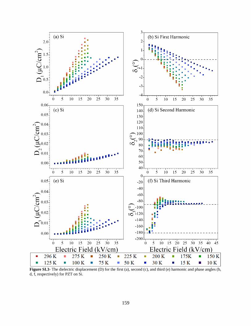
159
Figure SI.3- The dielectric displacement (D) for the first (a), second (c), and third (e) harmonic and phase angles (b,
d, f, respectively) for PZT on Si.
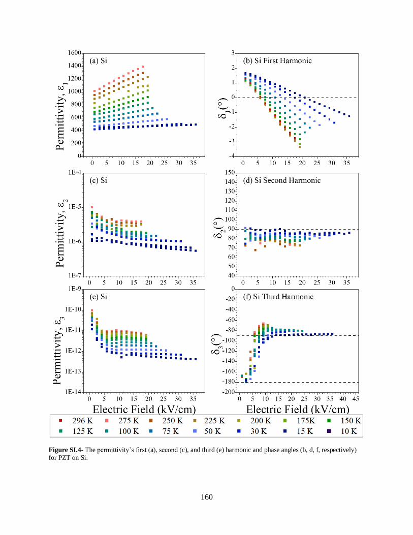
160
Figure SI.4- The permittivity’s first (a), second (c), and third (e) harmonic and phase angles (b, d, f, respectively)
for PZT on Si.
VITA
Kathleen Coleman
Kathleen Coleman was born in to Josie and Brian Coleman and grew up in Pearl River, NY with
her older brother, Michael, and younger sister, Maryanne. Kathleen graduated Pearl River high
school in June 2012. In July, Kathleen began her studies at the University of Connecticut in the
Bridge Engineering Diversity Program. After switching majors five times, she pursued her
bachelor in Materials Science and Engineering with a minor in Mathematics. In May 2016,
Kathleen received her bachelors of science and engineering summa cum lauda. In August 2016,
Kathleen joined Professor Susan Trolier-McKinstry’s group at the Pennsylvania State University.
Upon graduation, Kathleen will work at the Army Research Lab.