INA226 High-Side or Low-Side Measurement, Bi … · INA226 SBOS547A –JUNE 2011–REVISED AUGUST...
38
´ Power Register Current Register I C or SMBus Compatible 2 Interface Voltage Register GND VBUS ADC V I A0 A1 Alert SDA SCL C 0.1 F BYPASS m High- Side Shunt Low- Side Shunt Load Alert Register VS (Supply Voltage) Power Supply (0 V to 36 V) V IN+ V IN– Product Folder Sample & Buy Technical Documents Tools & Software Support & Community Reference Design INA226 SBOS547A – JUNE 2011 – REVISED AUGUST 2015 INA226 High-Side or Low-Side Measurement, Bi-Directional Current and Power Monitor with I 2 C Compatible Interface 1 Features 3 Description The INA226 is a current shunt and power monitor 1• Senses Bus Voltages From 0 V to 36 V with an I 2 C™- or SMBUS-compatible interface. The • High-Side or Low-Side Sensing device monitors both a shunt voltage drop and bus • Reports Current, Voltage, and Power supply voltage. Programmable calibration value, conversion times, and averaging, combined with an • High Accuracy: internal multiplier, enable direct readouts of current in – 0.1% Gain Error (Max) amperes and power in watts. – 10 μV Offset (Max) The INA226 senses current on common-mode bus • Configurable Averaging Options voltages that can vary from 0 V to 36 V, independent • 16 Programmable Addresses of the supply voltage. The device operates from a single 2.7-V to 5.5-V supply, drawing a typical of 330 • Operates from 2.7-V to 5.5-V Power Supply μA of supply current. The device is specified over the • 10-Pin, DGS (VSSOP) Package operating temperature range between –40°C and 125°C and features up to 16 programmable 2 Applications addresses on the I 2 C-compatible interface. • Servers Device Information (1) • Telecom Equipment PART NUMBER PACKAGE BODY SIZE (NOM) • Computing INA226 VSSOP (10) 3.00 mm x 3.00 mm • Power Management (1) For all available packages, see the orderable addendum at • Battery Chargers the end of the datasheet. • Power Supplies • Test Equipment High-Side or Low-Side Sensing Application 1 An IMPORTANT NOTICE at the end of this data sheet addresses availability, warranty, changes, use in safety-critical applications, intellectual property matters and other important disclaimers. PRODUCTION DATA.
Transcript of INA226 High-Side or Low-Side Measurement, Bi … · INA226 SBOS547A –JUNE 2011–REVISED AUGUST...

´ Power Register
Current Register I C or SMBusCompatible
2
Interface
Voltage Register
GND
VBUS
ADC
V
I
A0
A1
Alert
SDA
SCL
C
0.1 FBYPASS
m
High-Side
Shunt
Low-Side
Shunt
Load
Alert Register
VS(Supply Voltage)
Power Supply(0 V to 36 V)
VIN+
VIN–
Product
Folder
Sample &Buy
Technical
Documents
Tools &
Software
Support &Community
ReferenceDesign
INA226SBOS547A –JUNE 2011–REVISED AUGUST 2015
INA226 High-Side or Low-Side Measurement,Bi-Directional Current and Power Monitor with I2C Compatible Interface
1 Features 3 DescriptionThe INA226 is a current shunt and power monitor
1• Senses Bus Voltages From 0 V to 36 Vwith an I2C™- or SMBUS-compatible interface. The• High-Side or Low-Side Sensing device monitors both a shunt voltage drop and bus
• Reports Current, Voltage, and Power supply voltage. Programmable calibration value,conversion times, and averaging, combined with an• High Accuracy:internal multiplier, enable direct readouts of current in– 0.1% Gain Error (Max) amperes and power in watts.
– 10 μV Offset (Max)The INA226 senses current on common-mode bus• Configurable Averaging Options voltages that can vary from 0 V to 36 V, independent
• 16 Programmable Addresses of the supply voltage. The device operates from asingle 2.7-V to 5.5-V supply, drawing a typical of 330• Operates from 2.7-V to 5.5-V Power SupplyμA of supply current. The device is specified over the• 10-Pin, DGS (VSSOP) Packageoperating temperature range between –40°C and125°C and features up to 16 programmable2 Applications addresses on the I2C-compatible interface.
• ServersDevice Information(1)
• Telecom EquipmentPART NUMBER PACKAGE BODY SIZE (NOM)• Computing
INA226 VSSOP (10) 3.00 mm x 3.00 mm• Power Management(1) For all available packages, see the orderable addendum at• Battery Chargers the end of the datasheet.
• Power Supplies• Test Equipment
High-Side or Low-Side Sensing Application
1
An IMPORTANT NOTICE at the end of this data sheet addresses availability, warranty, changes, use in safety-critical applications,intellectual property matters and other important disclaimers. PRODUCTION DATA.

INA226SBOS547A –JUNE 2011–REVISED AUGUST 2015 www.ti.com
Table of Contents7.5 Programming .......................................................... 151 Features .................................................................. 17.6 Register Maps ......................................................... 212 Applications ........................................................... 1
8 Application and Implementation ........................ 283 Description ............................................................. 18.1 Application Information............................................ 284 Revision History..................................................... 28.2 Typical Applications ................................................ 285 Pin Configuration and Functions ......................... 3
9 Power Supply Recommendations ...................... 306 Specifications......................................................... 410 Layout................................................................... 306.1 Absolute Maximum Ratings ...................................... 4
10.1 Layout Guidelines ................................................. 306.2 ESD Ratings.............................................................. 410.2 Layout Example .................................................... 306.3 Recommended Operating Conditions....................... 4
11 Device and Documentation Support ................. 316.4 Thermal Information .................................................. 411.1 Device Support .................................................... 316.5 Electrical Characteristics........................................... 511.2 Community Resources.......................................... 316.6 Typical Characteristics .............................................. 711.3 Trademarks ........................................................... 317 Detailed Description ............................................ 1011.4 Electrostatic Discharge Caution............................ 317.1 Overview ................................................................. 1011.5 Glossary ................................................................ 317.2 Functional Block Diagram ....................................... 10
12 Mechanical, Packaging, and Orderable7.3 Feature Description................................................. 10Information ........................................................... 317.4 Device Functional Modes........................................ 13
4 Revision History
Changes from Original (June 2011) to Revision A Page
• Added Handling Rating table, Feature Description section, Device Functional Modes, Application andImplementation section, Power Supply Recommendations section, Layout section, Device and DocumentationSupport section, and Mechanical, Packaging, and Orderable Information section ............................................................... 1
2 Submit Documentation Feedback Copyright © 2011–2015, Texas Instruments Incorporated
Product Folder Links: INA226
GND
VS
VBUS
SCL
1
2
3
4
5
10
9
8
7
6
A1
A0
SDA
Alert
IN+
IN–
INA226www.ti.com SBOS547A –JUNE 2011–REVISED AUGUST 2015
5 Pin Configuration and Functions
DGS Package10-Pin VSSOP
Top View
Pin FunctionsPIN
I/O DESCRIPTIONNAME NO.
A0 2 Digital input Address pin. Connect to GND, SCL, SDA, or VS. Table 2 shows pin settings and corresponding addresses.
A1 1 Digital input Address pin. Connect to GND, SCL, SDA, or VS. Table 2 shows pin settings and corresponding addresses.
Alert 3 Digital output Multi-functional alert, open-drain output.
GND 7 Analog Ground.
IN+ 10 Analog input Connect to supply side of shunt resistor.
IN– 9 Analog input Connect to load side of shunt resistor.
SCL 5 Digital input Serial bus clock line, open-drain input.
SDA 4 Digital I/O Serial bus data line, open-drain input/output.
VBUS 8 Analog input Bus voltage input.
VS 6 Analog Power supply, 2.7 V to 5.5 V.
Copyright © 2011–2015, Texas Instruments Incorporated Submit Documentation Feedback 3
Product Folder Links: INA226

INA226SBOS547A –JUNE 2011–REVISED AUGUST 2015 www.ti.com
6 Specifications
6.1 Absolute Maximum Ratingsover operating free-air temperature range (unless otherwise noted) (1)
MIN MAX UNITVVS Supply voltage 6 V
Differential (VIN+ – VIN-) (2) –40 40Analog Inputs, VIN+, IN– Common-Mode (VIN+ + VIN-) / 2 –0.3 40VVBUS –0.3 40 VVSDA GND – 0.3 6 VVSCL GND – 0.3 VVS + 0.3 VIIN Input current into any pin 5 mAIOUT Open-drain digital output current 10 mATJ Junction temperature 150 °CTstg Storage temperature range –65 150 °C
(1) Stresses beyond those listed under Absolute Maximum Ratings may cause permanent damage to the device. These are stress ratingsonly, which do not imply functional operation of the device at these or any other conditions beyond those indicated under RecommendedOperating Conditions. Exposure to absolute-maximum-rated conditions for extended periods may affect device reliability.
(2) IN+ and IN– may have a differential voltage between –40 V and 40 V. However, the voltage at these pins must not exceed the range–0.3 V to 40 V.
6.2 ESD RatingsVALUE UNIT
Human body model (HBM), per ANSI/ESDA/JEDEC JS-001, all pins (1) ±2500Electrostatic Charged device model (CDM), per JEDEC specification JESD22-C101, allV(ESD) ±1000 Vdischarge pins (2)
Machine model (MM) ±150
(1) JEDEC document JEP155 states that 500-V HBM allows safe manufacturing with a standard ESD control process.(2) JEDEC document JEP157 states that 250-V CDM allows safe manufacturing with a standard ESD control process.
6.3 Recommended Operating Conditionsover operating free-air temperature range (unless otherwise noted)
MIN NOM MAX UNITVCM Common-mode input voltage 12 VVVS Operating supply voltage 3.3 VTA Operating free-air temperature –40 125 °C
6.4 Thermal InformationINA226
THERMAL METRIC (1) DGS (VSSOP) UNIT10 PINS
RθJA Junction-to-ambient thermal resistance 171.4 °C/WRθJC(top) Junction-to-case (top) thermal resistance 42.9 °C/WRθJB Junction-to-board thermal resistance 91.8 °C/WψJT Junction-to-top characterization parameter 1.5 °C/WψJB Junction-to-board characterization parameter 90.2 °C/WRθJC(bot) Junction-to-case (bottom) thermal resistance n/a °C/W
(1) For more information about traditional and new thermal metrics, see the Semiconductor and IC Package Thermal Metrics applicationreport, SPRA953.
4 Submit Documentation Feedback Copyright © 2011–2015, Texas Instruments Incorporated
Product Folder Links: INA226

INA226www.ti.com SBOS547A –JUNE 2011–REVISED AUGUST 2015
6.5 Electrical CharacteristicsTA = 25°C, VVS = 3.3 V, VIN+ = 12 V, VSENSE = (VIN+ – VIN–) = 0 mV and VVBUS = 12 V, unless otherwise noted
PARAMETER TEST CONDITIONS MIN TYP MAX UNITINPUT
Shunt voltage input range –81.9175 81.92 mVBus voltage input range (1) 0 36 V
CMRR Common-mode rejection 0 V ≤ VIN+ ≤ 36 V 126 140 dBVOS Shunt offset voltage, RTI (2) ±2.5 ±10 μV
Shunt offset voltage, RTI (2) vs –40°C ≤ TA ≤ 125°C 0.02 0.1 μV/°CtemperatureShunt offset voltage, RTI (2) vsPSRR 2.7 V ≤ VS ≤ 5.5 V 2.5 μV/VPower supply
VOS Bus offset voltage, RTI (2) ±1.25 ±7.5 mVBus offset voltage, RTI (2) vs –40°C ≤ TA ≤ 125°C 10 40 μV/°CtemperatureBus offset voltage, RTI (2) vs powerPSRR 0.5 mV/Vsupply
IB Input bias current (IIN+, IIN– pins) 10 μAVBUS input impedance 830 kΩ
(IN+ pin) + (IN– pin),Input leakage (3) 0.1 0.5 μAPower-down modeDC ACCURACY
ADC native resolution 16 BitsShunt voltage 2.5 μV
1 LSB step sizeBus voltage 1.25 mV
Shunt voltage gain error 0.02% 0.1%Shunt voltage gain error vs –40°C ≤ TA ≤ 125°C 10 50 ppm/°CtemperatureBus voltage gain error 0.02% 0.1%Bus voltage gain error vs –40°C ≤ TA ≤ 125°C 10 50 ppm/°CtemperatureDifferential nonlinearity ±0.1 LSB
CT bit = 000 140 154CT bit = 001 204 224
μsCT bit = 010 332 365CT bit = 011 588 646
tCT ADC conversion timeCT bit = 100 1.1 1.21CT bit = 101 2.116 2.328
msCT bit = 110 4.156 4.572CT bit = 111 8.244 9.068
SMBusSMBus timeout (4) 28 35 ms
(1) While the input range is 36 V, the full-scale range of the ADC scaling is 40.96 V. See the Basic ADC Functions section. Do not applymore than 36 V.
(2) RTI = Referred-to-input.(3) Input leakage is positive (current flowing into the pin) for the conditions shown at the top of this table. Negative leakage currents can
occur under different input conditions.(4) SMBus timeout in the INA226 resets the interface any time SCL is low for more than 28 ms.
Copyright © 2011–2015, Texas Instruments Incorporated Submit Documentation Feedback 5
Product Folder Links: INA226

INA226SBOS547A –JUNE 2011–REVISED AUGUST 2015 www.ti.com
Electrical Characteristics (continued)TA = 25°C, VVS = 3.3 V, VIN+ = 12 V, VSENSE = (VIN+ – VIN–) = 0 mV and VVBUS = 12 V, unless otherwise noted
PARAMETER TEST CONDITIONS MIN TYP MAX UNITDIGITAL INPUT/OUTPUT
Input capacitance 3 pF0 V ≤ VSCL ≤ VVS ,0 V ≤ VSDA ≤ VVS,
Leakage input current 0 V ≤ VAlert ≤ VVS , 0.1 1 μA0 V ≤ VA0 ≤ VVS ,0 V ≤ VA1 ≤ VVS
VIH High-level input voltage 0.7×VVS 6 VVIL Low-level input voltage –0.5 0.3×VVS VVOL Low-level output voltage, SDA, Alert IOL = 3 mA 0 0.4 V
Hysteresis 500 mVPOWER SUPPLY
Operating supply range 2.7 5.5 VIQ Quiescent current 330 420 μA
Quiescent current, power-down 0.5 2 μA(shutdown) modeVPOR Power-on reset threshold 2 V
6 Submit Documentation Feedback Copyright © 2011–2015, Texas Instruments Incorporated
Product Folder Links: INA226

Popula
tion
-100
-80
-60
-40
-20 0
20
40
60
80
100
Input Gain Error (m%)
0
100
200
300
400
500
600
−50 −25 0 25 50 75 100 125Temperature (°C)
Gai
n E
rror
(m
%)
G007
−2.4
−2.2
−2
−1.8
−1.6
−1.4
−1.2
−1
−50 −25 0 25 50 75 100 125Temperature (°C)
Offs
et (
µV)
G003
140
150
160
170
−50 −25 0 25 50 75 100 125Temperature (°C)
Com
mon
−M
ode
Rej
ectio
n R
atio
(dB
)
G004
Popula
tion
-10
-8
-6
-4
-2 0 2 4 6 8
10
Input Offset Voltage ( V)m
−60
−50
−40
−30
−20
−10
0
1 10 100 1k 10k 100kFrequency (Hz)
Gai
n (d
B)
G001
INA226www.ti.com SBOS547A –JUNE 2011–REVISED AUGUST 2015
6.6 Typical CharacteristicsAt TA = 25°C, VVS = 3.3 V, VIN+ = 12 V, VSENSE = (VIN+ – VIN–) = 0 mV and VVBUS = 12 V, unless otherwise noted.
Figure 2. Shunt Input Offset Voltage Production DistributionFigure 1. Frequency Response
Figure 3. Shunt Input Offset Voltage vs Temperature Figure 4. Shunt Input Common-Mode Rejection Ratio vsTemperature
Figure 5. Shunt Input Gain Error Production Distribution Figure 6. Shunt Input Gain Error vs Temperature
Copyright © 2011–2015, Texas Instruments Incorporated Submit Documentation Feedback 7
Product Folder Links: INA226

0
100
200
300
400
500
600
−50 −25 0 25 50 75 100 125Temperature (°C)
Gai
n E
rror
(m
%)
G012
0
5
10
15
20
25
0 4 8 12 16 20 24 28 32 36Common−Mode Input Voltage (V)
Inpu
t Bia
s C
urre
nt (
µA)
G012
Popula
tion
-100
-80
-60
-40
-20 0
20
40
60
80
100
Input Gain Error (m%)
−1.4
−1.2
−1.0
−0.8
−0.6
−50 −25 0 25 50 75 100 125Temperature (°C)
Offs
et (
mV
)
G009
Popula
tion
-7.5
-6
-4.5
-3
-1.5 0
1.5 3
4.5 6
7.5
Input Offset Voltage (mV)
−50
0
50
100
150
200
250
300
0 4 8 12 16 20 24 28 32 36Common−Mode Input Voltage (V)
Gai
n E
rror
(m
%)
G008
INA226SBOS547A –JUNE 2011–REVISED AUGUST 2015 www.ti.com
Typical Characteristics (continued)At TA = 25°C, VVS = 3.3 V, VIN+ = 12 V, VSENSE = (VIN+ – VIN–) = 0 mV and VVBUS = 12 V, unless otherwise noted.
Figure 8. Bus Input Offset Voltage Production DistributionFigure 7. Shunt Input Gain Error vs Common-Mode Voltage
Figure 10. Bus Input Gain Error Production DistributionFigure 9. Bus Input Offset Voltage vs Temperature
Figure 11. Bus Input Gain Error vs Temperature Figure 12. Input Bias Current vs Common-Mode Voltage
8 Submit Documentation Feedback Copyright © 2011–2015, Texas Instruments Incorporated
Product Folder Links: INA226

1 10 100 1,000 10,000
Frequency (kHz)
500
450
400
350
300
I(
A)
Qm
1 10 100 1,000 10,000
Frequency (kHz)
300
250
200
150
100
50
0
Shutd
ow
n I
(A
)Q
m
100
200
300
400
500
−50 −25 0 25 50 75 100 125Temperature (°C)
Qui
esce
nt C
urre
nt (
µA)
G015
0.2
0.4
0.6
0.8
1
1.2
−50 −25 0 25 50 75 100 125Temperature (°C)
Qui
esce
nt C
urre
nt −
Shu
tdow
n (µ
A)
G016
16
18
20
22
24
−50 −25 0 25 50 75 100 125Temperature (°C)
Inpu
t Bia
s C
urre
nt (
µA)
G013
20
60
100
140
180
220
260
−50 −25 0 25 50 75 100 125Temperature (°C)
Inpu
t Bia
s C
urre
nt −
Shu
tdow
n (n
A)
G014
INA226www.ti.com SBOS547A –JUNE 2011–REVISED AUGUST 2015
Typical Characteristics (continued)At TA = 25°C, VVS = 3.3 V, VIN+ = 12 V, VSENSE = (VIN+ – VIN–) = 0 mV and VVBUS = 12 V, unless otherwise noted.
Figure 13. Input Bias Current vs Temperature Figure 14. Input Bias Current vs Temperature, Shutdown
Figure 15. Active IQ vs Temperature Figure 16. Shutdown IQ vs Temperature
Figure 17. Active IQ vs I2C Clock Frequency Figure 18. Shutdown IQ vs I2C Clock Frequency
Copyright © 2011–2015, Texas Instruments Incorporated Submit Documentation Feedback 9
Product Folder Links: INA226

ADC
´
´
Shunt Voltage
Channel
Bus Voltage
Channel
Shunt Voltage(1)
Data Registers
Calibration(2)
Current(1)
Bus Voltage(1)
Power(1)
INA226SBOS547A –JUNE 2011–REVISED AUGUST 2015 www.ti.com
7 Detailed Description
7.1 OverviewThe INA226 is a digital current sense amplifier with an I2C- and SMBus-compatible interface. It provides digitalcurrent, voltage, and power readings necessary for accurate decision-making in precisely-controlled systems.Programmable registers allow flexible configuration for measurement resolution as well as continuous-versus-triggered operation. Detailed register information appears at the end of this data sheet, beginning with Table 4.See the Functional Block Diagram section for a block diagram of the INA226 device.
7.2 Functional Block Diagram
(1) Read-only(2) Read/write
7.3 Feature Description
7.3.1 Basic ADC FunctionsThe INA226 device performs two measurements on the power-supply bus of interest. The voltage developedfrom the load current that flows through a shunt resistor creates a shunt voltage that is measured at the IN+ andIN– pins. The device can also measure the power supply bus voltage by connecting this voltage to the VBUS pin.The differential shunt voltage is measured with respect to the IN– pin while the bus voltage is measured withrespect to ground.
The device is typically powered by a separate supply that can range from 2.7 V to 5.5 V. The bus that is beingmonitored can range in voltage from 0 V to 36 V. Based on the fixed 1.25-mV LSB for the Bus Voltage Registerthat a full-scale register results in a 40.96 V value.
NOTEDo not apply more than 36 V of actual voltage to the input pins.
There are no special considerations for power-supply sequencing because the common-mode input range andpower-supply voltage are independent of each other; therefore, the bus voltage can be present with the supplyvoltage off, and vice-versa.
The device takes two measurements, shunt voltage and bus voltage. It then converts these measurements tocurrent, based on the Calibration Register value, and then calculates power. Refer to the Programming theCalibration Register section for additional information on programming the Calibration Register.
10 Submit Documentation Feedback Copyright © 2011–2015, Texas Instruments Incorporated
Product Folder Links: INA226

INA226www.ti.com SBOS547A –JUNE 2011–REVISED AUGUST 2015
Feature Description (continued)The device has two operating modes, continuous and triggered, that determine how the ADC operates followingthese conversions. When the device is in the normal operating mode (that is, MODE bits of the ConfigurationRegister (00h) are set to '111'), it continuously converts a shunt voltage reading followed by a bus voltagereading. After the shunt voltage reading, the current value is calculated (based on Equation 3). This current valueis then used to calculate the power result (using Equation 4). These values are subsequently stored in anaccumulator, and the measurement/calculation sequence repeats until the number of averages set in theConfiguration Register (00h) is reached. Following every sequence, the present set of values measured andcalculated are appended to previously collected values. After all of the averaging has been completed, the finalvalues for shunt voltage, bus voltage, current, and power are updated in the corresponding registers that canthen be read. These values remain in the data output registers until they are replaced by the next fully completedconversion results. Reading the data output registers does not affect a conversion in progress.
The mode control in the Conversion Register (00h) also permits selecting modes to convert only the shuntvoltage or the bus voltage in order to further allow the user to configure the monitoring function to fit the specificapplication requirements.
All current and power calculations are performed in the background and do not contribute to conversion time.
In triggered mode, writing any of the triggered convert modes into the Configuration Register (00h) (that is,MODE bits of the Configuration Register (00h) are set to ‘001’, ‘010’, or ‘011’) triggers a single-shot conversion.This action produces a single set of measurements; thus, to trigger another single-shot conversion, theConfiguration Register (00h) must be written to a second time, even if the mode does not change.
In addition to the two operating modes (continuous and triggered), the device also has a power-down mode thatreduces the quiescent current and turns off current into the device inputs, reducing the impact of supply drainwhen the device is not being used. Full recovery from power-down mode requires 40µs. The registers of thedevice can be written to and read from while the device is in power-down mode. The device remains in power-down mode until one of the active modes settings are written into the Configuration Register (00h) .
Although the device can be read at any time, and the data from the last conversion remain available, theConversion Ready flag bit (Mask/Enable Register, CVRF bit) is provided to help coordinate one-shot or triggeredconversions. The Conversion Ready flag (CVRF) bit is set after all conversions, averaging, and multiplicationoperations are complete.
The Conversion Ready flag (CVRF) bit clears under these conditions:• Writing to the Configuration Register (00h), except when configuring the MODE bits for power-down mode; or• Reading the Mask/Enable Register (06h)
7.3.1.1 Power CalculationThe Current and Power are calculated following shunt voltage and bus voltage measurements as shown inFigure 19. Current is calculated following a shunt voltage measurement based on the value set in the CalibrationRegister. If there is no value loaded into the Calibration Register, the current value stored is zero. Power iscalculated following the bus voltage measurement based on the previous current calculation and bus voltagemeasurement. If there is no value loaded in the Calibration Register, the power value stored is also zero. Again,these calculations are performed in the background and do not add to the overall conversion time. These currentand power values are considered intermediate results (unless the averaging is set to 1) and are stored in aninternal accumulation register, not the corresponding output registers. Following every measured sample, thenewly-calculated values for current and power are appended to this accumulation register until all of the sampleshave been measured and averaged based on the number of averages set in the Configuration Register (00h).
Copyright © 2011–2015, Texas Instruments Incorporated Submit Documentation Feedback 11
Product Folder Links: INA226

I I I II I I II I I II I I IV V V VV V V VV V V VV V V V
P P P P P P P P P P P P P P P P
Current Limit Detect Following
Every Shunt Voltage Conversion
Bus and Power Limit Detect
Following Every Bus Voltage Conversion
Power Average
Bus Voltage Average
Shunt Voltage Average
INA226SBOS547A –JUNE 2011–REVISED AUGUST 2015 www.ti.com
Feature Description (continued)
Figure 19. Power Calculation Scheme
In addition to the current and power accumulating after every sample, the shunt and bus voltage measurementsare also collected. After all of the samples have been measured and the corresponding current and powercalculations have been made, the accumulated average for each of these parameters is then loaded to thecorresponding output registers, where they can then be read.
7.3.1.2 Alert PinThe INA226 has a single Alert Limit Register (07h), that allows the Alert pin to be programmed to respond to asingle user-defined event or to a Conversion Ready notification if desired. The Mask/Enable Register allows theuser to select from one of the five available functions to monitor and/or set the Conversion Ready bit to controlthe response of the Alert pin. Based on the function being monitored, the user would then enter a value into theAlert Limit Register to set the corresponding threshold value that asserts the Alert pin.
The Alert pin allows for one of several available alert functions to be monitored to determine if a user-definedthreshold has been exceeded. The five alert functions that can be monitored are:• Shunt Voltage Over-Limit (SOL)• Shunt Voltage Under-Limit (SUL)• Bus Voltage Over-Limit (BOL)• Bus Voltage Under-Limit (BUL)• Power Over-Limit (POL)
The Alert pin is an open-drain output. This pin is asserted when the alert function selected in the Mask/EnableRegister exceeds the value programmed into the Alert Limit Register. Only one of these alert functions can beenabled and monitored at a time. If multiple alert functions are enabled, the selected function in the highestsignificant bit position takes priority and responds to the Alert Limit Register value. For example, if the ShuntVoltage Over-Limit function and the Shunt Voltage Under-Limit function are both selected, the Alert pin assertswhen the Shunt Voltage Register exceeds the value in the Alert Limit Register.
The Conversion Ready state of the device can also be monitored at the Alert pin to inform the user when thedevice has completed the previous conversion and is ready to begin a new conversion. Conversion Ready canbe monitored at the Alert pin along with one of the alert functions. If an alert function and the Conversion Readyare both enabled to be monitored at the Alert pin, after the Alert pin is asserted, the Mask/Enable Register mustbe read following the alert to determine the source of the alert. By reading the Conversion Ready Flag (CVRF, bit3), and the Alert Function Flag (AFF, bit 4) in the Mask/Enable Register, the source of the alert can bedetermined. If the Conversion Ready feature is not desired and the CNVR bit is not set, the Alert pin onlyresponds to an exceeded alert limit based on the alert function enabled.
If the alert function is not used, the Alert pin can be left floating without impacting the operation of the device.
12 Submit Documentation Feedback Copyright © 2011–2015, Texas Instruments Incorporated
Product Folder Links: INA226

10
V/d
ivm
Number of Conversions
0 200 400 600 800 1000
Conversion Time: 140 sm
Conversion Time: 1.1ms
Conversion Time: 8.244ms
INA226www.ti.com SBOS547A –JUNE 2011–REVISED AUGUST 2015
Feature Description (continued)Refer to Figure 19 to see the relative timing of when the value in the Alert Limit Register is compared to thecorresponding converted value. For example, if the alert function that is enabled is Shunt Voltage Over-Limit(SOL), following every shunt voltage conversion the value in the Alert Limit Register is compared to themeasured shunt voltage to determine if the measurements has exceeded the programmed limit. The AFF, bit 4 ofthe Mask/Enable Register, asserts high any time the measured voltage exceeds the value programmed into theAlert Limit Register. In addition to the AFF being asserted, the Alert pin is asserted based on the Alert Polarity Bit(APOL, bit 1 of the Mask/Enable Register). If the Alert Latch is enabled, the AFF and Alert pin remain asserteduntil either the Configuration Register (00h) is written to or the Mask/Enable Register is read.
The Bus Voltage alert functions compare the measured bus voltage to the Alert Limit Register following everybus voltage conversion and assert the AFF bit and Alert pin if the limit threshold is exceeded.
The Power Over-Limit alert function is also compared to the calculated power value following every bus voltagemeasurement conversion and asserts the AFF bit and Alert pin if the limit threshold is exceeded.
7.4 Device Functional Modes
7.4.1 Averaging and Conversion Time ConsiderationsThe INA226 device offers programmable conversion times (tCT) for both the shunt voltage and bus voltagemeasurements. The conversion times for these measurements can be selected from as fast as 140 μs to as longas 8.244 ms. The conversion time settings, along with the programmable averaging mode, allow the device to beconfigured to optimize the available timing requirements in a given application. For example, if a system requiresthat data be read every 5ms, the device could be configured with the conversion times set to 588 μs for bothshunt and bus voltage measurements and the averaging mode set to 4. This configuration results in the dataupdating approximately every 4.7ms. The device could also be configured with a different conversion time settingfor the shunt and bus voltage measurements. This type of approach is common in applications where the busvoltage tends to be relatively stable. This situation can allow for the time focused on the bus voltagemeasurement to be reduced relative to the shunt voltage measurement. The shunt voltage conversion time couldbe set to 4.156 ms with the bus voltage conversion time set to 588 μs, with the averaging mode set to 1. Thisconfiguration also results in data updating approximately every 4.7 ms.
There are trade-offs associated with the settings for conversion time and the averaging mode used. Theaveraging feature can significantly improve the measurement accuracy by effectively filtering the signal. Thisapproach allows the device to reduce any noise in the measurement that may be caused by noise coupling intothe signal. A greater number of averages enables the device to be more effective in reducing the noisecomponent of the measurement.
The conversion times selected can also have an impact on the measurement accuracy. Figure 20 shows multipleconversion times to illustrate the impact of noise on the measurement. In order to achieve the highest accuracymeasurement possible, use a combination of the longest allowable conversion times and highest number ofaverages, based on the timing requirements of the system.
Figure 20. Noise vs Conversion Time
Copyright © 2011–2015, Texas Instruments Incorporated Submit Documentation Feedback 13
Product Folder Links: INA226
Power Register
Current Register I C or SMBusCompatible
2
Interface
Voltage Register
GND
VBUS
ADC
V
I
A0
Alert
A1
SDA
SCL
C
0.1 µFBYPASS
LoadAlert Register
VS(Supply Voltage)
Power Supply(0 V to 36 V)
C
0.1 µF to 1 µFCeramic
Capacitor
FILTER
VIN-
VIN+
XRFILTER
≤ 10 Ω
RFILTER
≤ 10 Ω
INA226SBOS547A –JUNE 2011–REVISED AUGUST 2015 www.ti.com
Device Functional Modes (continued)7.4.2 Filtering and Input ConsiderationsMeasuring current is often noisy, and such noise can be difficult to define. The INA226 device offers severaloptions for filtering by allowing the conversion times and number of averages to be selected independently in theConfiguration Register (00h). The conversion times can be set independently for the shunt voltage and busvoltage measurements to allow added flexibility in configuring the monitoring of the power-supply bus.
The internal ADC is based on a delta-sigma (ΔΣ) front-end with a 500 kHz (±30%) typical sampling rate. Thisarchitecture has good inherent noise rejection; however, transients that occur at or very close to the samplingrate harmonics can cause problems. Because these signals are at 1 MHz and higher, they can be managed byincorporating filtering at the input of the device. The high frequency enables the use of low-value series resistorson the filter with negligible effects on measurement accuracy. In general, filtering the device input is onlynecessary if there are transients at exact harmonics of the 500 kHz (±30%) sampling rate (greater than 1 MHz).Filter using the lowest possible series resistance (typically 10 Ω or less) and a ceramic capacitor. Recommendedvalues for this capacitor are between 0.1 μF and 1 μF. Figure 21 shows the device with a filter added at theinput.
Overload conditions are another consideration for the device inputs. The device inputs are specified to tolerate40 V across the inputs. A large differential scenario might be a short to ground on the load side of the shunt. Thistype of event can result in full power-supply voltage across the shunt (as long the power supply or energystorage capacitors support it). Removing a short to ground can result in inductive kickbacks that could exceedthe 40-V differential and common-mode rating of the device. Inductive kickback voltages are best controlled byZener-type transient-absorbing devices (commonly called transzorbs) combined with sufficient energy storagecapacitance. See the TI Design, Transient Robustness for Current Shunt Monitors (TIDU473), which describes ahigh-side current shunt monitor used to measure the voltage developed across a current-sensing resistor whencurrent passes through it.
In applications that do not have large energy storage electrolytics on one or both sides of the shunt, an inputoverstress condition may result from an excessive dV/dt of the voltage applied to the input. A hard physical shortis the most likely cause of this event, particularly in applications with no large electrolytics present. This problemoccurs because an excessive dV/dt can activate the ESD protection in the device in systems where largecurrents are available. Testing demonstrates that the addition of 10-Ω resistors in series with each input of thedevice sufficiently protects the inputs against this dV/dt failure up to the 40-V rating of the device. Selecting theseresistors in the range noted has minimal effect on accuracy.
Figure 21. Input Filtering
14 Submit Documentation Feedback Copyright © 2011–2015, Texas Instruments Incorporated
Product Folder Links: INA226
ShuntVoltage CalibrationRegister
2048
·
Current =
Maximum Expected Current
215Current_LSB =
CAL =0.00512
Current_LSB RSHUNT·
INA226www.ti.com SBOS547A –JUNE 2011–REVISED AUGUST 2015
7.5 ProgrammingAn important aspect of the INA226 device is that it does not necessarily measure current or power. The devicemeasures both the differential voltage applied between the IN+ and IN- input pins and the voltage applied to theVBUS pin. In order for the device to report both current and power values, the user must program the resolutionof the Current Register (04h) and the value of the shunt resistor present in the application to develop thedifferential voltage applied between the input pins. The Power Register (03h) is internally set to be 25 times theprogrammed Current_LSB. Both the Current_LSB and shunt resistor value are used in the calculation of theCalibration Register value the device uses to calculate the corresponding current and power values based on themeasured shunt and bus voltages.
The Calibration Register is calculated based on Equation 1. This equation includes the term Current_LSB, whichis the programmed value for the LSB for the Current Register (04h). The user uses this value to convert thevalue in the Current Register (04h) to the actual current in amperes. The highest resolution for the CurrentRegister (04h) can be obtained by using the smallest allowable Current_LSB based on the maximum expectedcurrent as shown in Equation 2. While this value yields the highest resolution, it is common to select a value forthe Current_LSB to the nearest round number above this value to simplify the conversion of the Current Register(04h) and Power Register (03h) to amperes and watts respectively. The RSHUNT term is the value of the externalshunt used to develop the differential voltage across the input pins.
where• 0.00512 is an internal fixed value used to ensure scaling is maintained properly (1)
(2)
After programming the Calibration Register, the Current Register (04h) and Power Register (03h) updateaccordingly based on the corresponding shunt voltage and bus voltage measurements. Until the CalibrationRegister is programmed, the Current Register (04h) and Power Register (03h) remain at zero.
7.5.1 Programming the Calibration RegisterFigure 27 shows a nominal 10-A load that creates a differential voltage of 20 mV across a 2-mΩ shunt resistor.The bus voltage for the INA226 is measured at the external VBUS input pin, which in this example is connectedto the IN– pin to measure the voltage level delivered to the load. For this example, the VBUS pin measures lessthan 12 V because the voltage at the IN– pin is 11.98 V as a result of the voltage drop across the shunt resistor.
For this example, assuming a maximum expected current of 15 A, the Current_LSB is calculated to be 457.7μA/bit using Equation 2. Using a value for the Current_LSB of 500 μA/Bit or 1 mA/Bit would significantly simplifythe conversion from the Current Register (04h) and Power Register (03h) to amperes and watts. For thisexample, a value of 1 mA/bit was chosen for the Current_LSB. Using this value for the Current_LSB does trade asmall amount of resolution for having a simpler conversion process on the user side. Using Equation 1 in thisexample with a Current_LSB value of 1 mA/bit and a shunt resistor of 2 mΩ results in a Calibration Registervalue of 2560, or A00h.
The Current Register (04h) is then calculated by multiplying the decimal value of the Shunt Voltage Register(01h) contents by the decimal value of the Calibration Register and then dividing by 2048, as shown inEquation 3. For this example, the Shunt Voltage Register contains a value of 8,000 (representing 20 mV), whichis multiplied by the Calibration Register value of 2560 and then divided by 2048 to yield a decimal value for theCurrent Register (04h) of 10000, or 2710h. Multiplying this value by 1 mA/bit results in the original 10-A levelstated in the example.
(3)
Copyright © 2011–2015, Texas Instruments Incorporated Submit Documentation Feedback 15
Product Folder Links: INA226

Corrected_Full_Scale_Cal = truncCal MeasShuntCurrent
INA226_Current
´
Current BusVoltage
20,000
·
Power =
INA226SBOS547A –JUNE 2011–REVISED AUGUST 2015 www.ti.com
Programming (continued)The LSB for the Bus Voltage Register (02h) is a fixed 1.25 mV/bit, which means that the 11.98 V present at theVBUS pin results in a register value of 2570h, or a decimal equivalent of 9584. Note that the MSB of the BusVoltage Register (02h) is always zero because the VBUS pin is only able to measure positive voltages.
The Power Register (03h) is then be calculated by multiplying the decimal value of the Current Register, 10000,by the decimal value of the Bus Voltage Register (02h), 9584, and then dividing by 20,000, as defined inEquation 4. For this example, the result for the Power Register (03h) is 12B8h, or a decimal equivalent of 4792.Multiplying this result by the power LSB (25 times the [1 × 10⁻³ Current_LSB]) results in a power calculation of(4792 × 25 mW/bit), or 119.82 W. The power LSB has a fixed ratio to the Current_LSB of 25. For this example, aprogrammed 1 mA/bit Current_LSB results in a power LSB of 25 mW/bit. This ratio is internally programmed toensure that the scaling of the power calculation is within an acceptable range. A manual calculation for the powerbeing delivered to the load would use a bus voltage of 11.98 V (12 VCM – 20 mV shunt drop) multiplied by theload current of 10 A to give a result of 119.8 W.
(4)
Table 1 lists the steps for configuring, measuring, and calculating the values for current and power for thisdevice.
Table 1. Calculating Current and Power (1)
STEP REGISTER NAME ADDRESS CONTENTS DEC LSB VALUEStep 1 Configuration Register 00h 4127h — — —Step 2 Shunt Register 01h 1F40h 8000 2.5 µV 20 mVStep 3 Bus Voltage Register 02h 2570h 9584 1.25 mV 11.98 VStep 4 Calibration Register 05h A00h 2560 — —Step 5 Current Register 04h 2710 10000 1 mA 10 AStep 6 Power Register 03h 12B8h 4792 25 mW 119.82 W
(1) Conditions: Load = 10 A, VCM = 12 V, RSHUNT = 2 mΩ, and VVBUS = 12 V.
7.5.2 Programming the Power Measurement Engine
7.5.2.1 Calibration Register and ScalingThe Calibration Register enables the user to scale the Current Register (04h) and Power Register (03h) to themost useful value for a given application. For example, set the Calibration Register such that the largest possiblenumber is generated in the Current Register (04h) or Power Register (03h) at the expected full-scale point. Thisapproach yields the highest resolution using the previously calculated minimum Current_LSB in the equation forthe Calibration Register. The Calibration Register can also be selected to provide values in the Current Register(04h) and Power Register (03h) that either provide direct decimal equivalents of the values being measured, oryield a round LSB value for each corresponding register. After these choices have been made, the CalibrationRegister also offers possibilities for end user system-level calibration. After determining the exact current byusing an external ammeter, the value of the Calibration Register can then be adjusted based on the measuredcurrent result of the INA226 to cancel the total system error as shown in Equation 5.
(5)
7.5.3 Simple Current Shunt Monitor Usage (No Programming Necessary)The device can be used without any programming if it is only necessary to read a shunt voltage drop and busvoltage with the default power-on reset configuration and continuous conversion of shunt and bus voltages.
16 Submit Documentation Feedback Copyright © 2011–2015, Texas Instruments Incorporated
Product Folder Links: INA226

INA226www.ti.com SBOS547A –JUNE 2011–REVISED AUGUST 2015
Without programming the device Calibration Register, the device is unable to provide either a valid current orpower value, because these outputs are both derived using the values loaded into the Calibration Register.
7.5.4 Default SettingsThe default power-up states of the registers are shown in the Register Maps section of this data sheet. Theseregisters are volatile, and if programmed to a value other than the default values shown in Table 4, they must bere-programmed at every device power-up. Detailed information on programming the Calibration Registerspecifically is given in the Programming section and calculated based on Equation 1.
7.5.5 Bus OverviewThe INA226 offers compatibility with both I2C and SMBus interfaces. The I2C and SMBus protocols areessentially compatible with one another.
The I2C interface is used throughout this data sheet as the primary example, with SMBus protocol specified onlywhen a difference between the two systems is discussed. Two lines, SCL and SDA, connect the device to thebus. Both SCL and SDA are open-drain connections.
The device that initiates a data transfer is called a master, and the devices controlled by the master are slaves.The bus must be controlled by a master device that generates the serial clock (SCL), controls the bus access,and generates START and STOP conditions.
To address a specific device, the master initiates a start condition by pulling the data signal line (SDA) from ahigh to a low logic level while SCL is high. All slaves on the bus shift in the slave address byte on the rising edgeof SCL, with the last bit indicating whether a read or write operation is intended. During the ninth clock pulse, theslave being addressed responds to the master by generating an Acknowledge and pulling SDA low.
Data transfer is then initiated and eight bits of data are sent, followed by an Acknowledge bit. During datatransfer, SDA must remain stable while SCL is high. Any change in SDA while SCL is high is interpreted as astart or stop condition.
After all data have been transferred, the master generates a stop condition, indicated by pulling SDA from low tohigh while SCL is high. The device includes a 28 ms timeout on its interface to prevent locking up the bus.
Copyright © 2011–2015, Texas Instruments Incorporated Submit Documentation Feedback 17
Product Folder Links: INA226
INA226SBOS547A –JUNE 2011–REVISED AUGUST 2015 www.ti.com
7.5.5.1 Serial Bus AddressTo communicate with the INA226, the master must first address slave devices via a slave address byte. Theslave address byte consists of seven address bits and a direction bit that indicates whether the action is to be aread or write operation.
The device has two address pins, A0 and A1. Table 2 lists the pin logic levels for each of the 16 possibleaddresses. The device samples the state of pins A0 and A1 on every bus communication. Establish the pinstates before any activity on the interface occurs.
Table 2. Address Pins and Slave AddressesA1 A0 SLAVE ADDRESS
GND GND 1000000GND VS 1000001GND SDA 1000010GND SCL 1000011VS GND 1000100VS VS 1000101VS SDA 1000110VS SCL 1000111
SDA GND 1001000SDA VS 1001001SDA SDA 1001010SDA SCL 1001011SCL GND 1001100SCL VS 1001101SCL SDA 1001110SCL SCL 1001111
7.5.5.2 Serial InterfaceThe INA226 operates only as a slave device on both the I2C bus and the SMBus. Connections to the bus aremade via the open-drain SDA and SCL lines. The SDA and SCL pins feature integrated spike suppression filtersand Schmitt triggers to minimize the effects of input spikes and bus noise. Although the device integrates spikesuppression into the digital I/O lines, proper layout techniques help minimize the amount of coupling into thecommunication lines. This noise introduction could occur from capacitively coupling signal edges between thetwo communication lines themselves or from other switching noise sources present in the system. Routing tracesin parallel with ground in between layers on a printed circuit board (PCB) typically reduces the effects of couplingbetween the communication lines. Shielded communication lines reduces the possibility of unintended noisecoupling into the digital I/O lines that could be incorrectly interpreted as start or stop commands.
The INA226 supports the transmission protocol for fast mode (1 kHz to 400 kHz) and high-speed mode (1 kHz to2.94 MHz). All data bytes are transmitted most significant byte first.
7.5.5.3 Writing to and Reading from the INA226Accessing a specific register on the INA226 is accomplished by writing the appropriate value to the registerpointer. Refer to Table 4 for a complete list of registers and corresponding addresses. The value for the registerpointer (as shown in Figure 25) is the first byte transferred after the slave address byte with the R/W bit low.Every write operation to the device requires a value for the register pointer.
Writing to a register begins with the first byte transmitted by the master. This byte is the slave address, with theR/W bit low. The device then acknowledges receipt of a valid address. The next byte transmitted by the master isthe address of the register which data is written to. This register address value updates the register pointer to thedesired register. The next two bytes are written to the register addressed by the register pointer. The deviceacknowledges receipt of each data byte. The master may terminate data transfer by generating a start or stopcondition.
18 Submit Documentation Feedback Copyright © 2011–2015, Texas Instruments Incorporated
Product Folder Links: INA226

Frame 1 Two-Wire Slave Address Byte(1)
Frame 2 Data MSByte(2)
1
Start By
Master
ACK By
Slave
ACK By
Master
From
Slave
1 9 1 9
SDA
SCL
0 0 A3 R/W D15 D14 D13 D12 D11 D10 D9 D8A2 A1 A0
Frame 3 Data LSByte(2)
StopNo ACK By(3)
Master
From
Slave
1 9
D7 D6 D5 D4 D3 D2 D1 D0
Frame 1 Two-Wire Slave Address Byte(1)
Frame 2 Register Pointer Byte
Start By
Master
ACK By
Slave
ACK By
Slave
1 9 1
ACK By
Slave
1
D15 D14 D13 D12 D11 D10 D9 D8
99
SDA
SCL
1 0 0 A3 A2 A1 A0 R/W P7 P6 P5 P4 P3 P2 P1 P0
Frame 4 Data LSByteFrame 3 Data MSByte
ACK By
Slave
Stop By
Master
1
D7 D6 D5 D4 D3 D2 D1 D0
9
INA226www.ti.com SBOS547A –JUNE 2011–REVISED AUGUST 2015
When reading from the device , the last value stored in the register pointer by a write operation determines whichregister is read during a read operation. To change the register pointer for a read operation, a new value must bewritten to the register pointer. This write is accomplished by issuing a slave address byte with the R/W bit low,followed by the register pointer byte. No additional data are required. The master then generates a start conditionand sends the slave address byte with the R/W bit high to initiate the read command. The next byte istransmitted by the slave and is the most significant byte of the register indicated by the register pointer. This byteis followed by an Acknowledge from the master; then the slave transmits the least significant byte. The masteracknowledges receipt of the data byte. The master may terminate data transfer by generating a Not-Acknowledge after receiving any data byte, or generating a start or stop condition. If repeated reads from thesame register are desired, it is not necessary to continually send the register pointer bytes; the device retains theregister pointer value until it is changed by the next write operation.
Figure 22 shows the write operation timing diagram. Figure 23 shows the read operation timing diagram.
NOTERegister bytes are sent most-significant byte first, followed by the least significant byte.
(1) The value of the Slave Address byte is determined by the settings of the A0 and A1 pins. Refer to Table 2.
Figure 22. Timing Diagram for Write Word Format
(1) The value of the Slave Address byte is determined by the settings of the A0 and A1 pins. Refer to Table 2.(2) Read data is from the last register pointer location. If a new register is desired, the register pointer must be updated.
See Figure 25.(3) ACK by Master can also be sent.
Figure 23. Timing Diagram for Read Word Format
Figure 24 shows the timing diagram for the SMBus Alert response operation. Figure 25 illustrates a typicalregister pointer configuration.
Copyright © 2011–2015, Texas Instruments Incorporated Submit Documentation Feedback 19
Product Folder Links: INA226

SCL
SDA
t(LOW)tR tF t(HDSTA)
t(HDSTA)
t(HDDAT) t(SUDAT)
t(HIGH) t(SUSTA)t(SUSTO)
t(BUF)
S SP P
Frame 1 Two-Wire Slave Address Byte(1)
Frame 2 Register Pointer Byte
1
Start By
Master
ACK By
Slave
ACK By
Slave
1 9 1 9
SDA
SCL
0 0 A3 A2 A1 A0 R/W P7 P6 P5 P4 P3 P2 P1 P0 Stop
¼
Frame 1 SMBus ALERT Response Address Byte Frame 2 Slave Address Byte(1)
Start By
Master
ACK By
Slave
From
Slave
NACK By
Master
Stop By
Master
1 9 1 9
SDA
SCL
ALERT
0 0 0 1 1 0 0 R/W 1 0 0 A3 A2 A1 A0 0
INA226SBOS547A –JUNE 2011–REVISED AUGUST 2015 www.ti.com
(1) The value of the Slave Address Byte is determined by the settings of the A0 and A1 pins. Refer to Table 2.
Figure 24. Timing Diagram for SMBus ALERT
(1) The value of the Slave Address Byte is determined by the settings of the A0 and A1 pins. Refer to Table 2.
Figure 25. Typical Register Pointer Set
7.5.5.3.1 High-Speed I2C Mode
When the bus is idle, both the SDA and SCL lines are pulled high by the pullup resistors. The master generatesa start condition followed by a valid serial byte containing high-speed (HS) master code 00001XXX. Thistransmission is made in fast (400 kHz) or standard (100 kHz) (F/S) mode at no more than 400 kHz. The devicedoes not acknowledge the HS master code, but does recognize it and switches its internal filters to support 2.94MHz operation.
The master then generates a repeated start condition (a repeated start condition has the same timing as the startcondition). After this repeated start condition, the protocol is the same as F/S mode, except that transmissionspeeds up to 2.94 MHz are allowed. Instead of using a stop condition, use repeated start conditions to securethe bus in HS-mode. A stop condition ends the HS-mode and switches all the internal filters of the device tosupport the F/S mode.
Figure 26. Bus Timing Diagram
20 Submit Documentation Feedback Copyright © 2011–2015, Texas Instruments Incorporated
Product Folder Links: INA226

INA226www.ti.com SBOS547A –JUNE 2011–REVISED AUGUST 2015
Table 3. Bus Timing Diagram Definitions (1)
FAST MODE HIGH-SPEED MODEPARAMETER MIN MAX MIN MAX UNIT
SCL operating frequency f(SCL) 0.001 0.4 0.001 2.94 MHzBus free time between stop and start t(BUF) 600 160 nsconditionsHold time after repeated START condition. t(HDSTA) 100 100 nsAfter this period, the first clock is generated.Repeated start condition setup time t(SUSTA) 100 100 nsSTOP condition setup time t(SUSTO) 100 100 nsData hold time t(HDDAT) 10 900 10 100 nsData setup time t(SUDAT) 100 20 nsSCL clock low period t(LOW) 1300 200 nsSCL clock high period t(HIGH) 600 60 nsData fall time tF 300 80 nsClock fall time tF 300 40 nsClock rise time tR 300 40 nsClock/data rise time for SCLK ≤ 100kHz tR 1000 ns
(1) Values based on a statistical analysis of a one-time sample of devices. Minimum and maximum values are not guaranteed and notproduction tested.
7.5.5.4 SMBus Alert ResponseThe INA226 is designed to respond to the SMBus Alert Response address. The SMBus Alert Response providesa quick fault identification for simple slave devices. When an Alert occurs, the master can broadcast the AlertResponse slave address (0001 100) with the Read/Write bit set high. Following this Alert Response, any slavedevice that generates an alert identifies itself by acknowledging the Alert Response and sending its address onthe bus.
The Alert Response can activate several different slave devices simultaneously, similar to the I2C General Call. Ifmore than one slave attempts to respond, bus arbitration rules apply. The losing device does not generate anAcknowledge and continues to hold the Alert line low until the interrupt is cleared.
7.6 Register MapsThe INA226 uses a bank of registers for holding configuration settings, measurement results, minimum/maximumlimits, and status information. Table 4 summarizes the device registers; refer to the Functional Block Diagramsection for an illustration of the registers.
All 16-bit device registers are two 8-bit bytes via the I2C interface.
Table 4. Register Set SummaryPOINTERADDRESS POWER-ON RESET
HEX REGISTER NAME FUNCTION BINARY HEX TYPE (1)
All-register reset, shunt voltage and bus00h Configuration Register voltage ADC conversion times and 01000001 00100111 4127 R/W
averaging, operating mode.01h Shunt Voltage Register Shunt voltage measurement data. 00000000 00000000 0000 R02h Bus Voltage Register Bus voltage measurement data. 00000000 00000000 0000 R
Contains the value of the calculated03h Power Register (2) 00000000 00000000 0000 Rpower being delivered to the load.Contains the value of the calculated
04h Current Register (2) current flowing through the shunt 00000000 00000000 0000 Rresistor.
(1) Type: R = Read-Only, R/W = Read/Write.(2) The Current Register (04h) and Power Register (03h) default to '0' because the Calibration register defaults to '0', yielding zero current
and power values until the Calibration register is programmed.
Copyright © 2011–2015, Texas Instruments Incorporated Submit Documentation Feedback 21
Product Folder Links: INA226

INA226SBOS547A –JUNE 2011–REVISED AUGUST 2015 www.ti.com
Register Maps (continued)Table 4. Register Set Summary (continued)
POINTERADDRESS POWER-ON RESET
HEX REGISTER NAME FUNCTION BINARY HEX TYPE (1)
Sets full-scale range and LSB of current05h Calibration Register and power measurements. Overall 00000000 00000000 0000 R/W
system calibration.Alert configuration and Conversion06h Mask/Enable Register 00000000 00000000 0000 R/WReady flag.Contains the limit value to compare to07h Alert Limit Register 00000000 00000000 0000 R/Wthe selected Alert function.Contains unique manufacturerFEh Manufacturer ID Register 0101010001001001 5449 Ridentification number.Contains unique die identificationFFh Die ID Register 0010001001100000 2260 Rnumber.
7.6.1 Configuration Register (00h) (Read/Write)
Table 5. Configuration Register (00h) (Read/Write) DescriptionsBIT NO. D15 D14 D13 D12 D11 D10 D9 D8 D7 D6 D5 D4 D3 D2 D1 D0
BIT RST — — — AVG2 AVG1 AVG0 VBUSCT2 VBUSCT1 VBUSCT0 VSHCT2 VSHCT1 VSHCT0 MODE3 MODE2 MODE1NAME
POR 0 1 0 0 0 0 0 1 0 0 1 0 0 1 1 1VALUE
The Configuration Register settings control the operating modes for the device. This register controls theconversion time settings for both the shunt and bus voltage measurements as well as the averaging mode used.The operating mode that controls what signals are selected to be measured is also programmed in theConfiguration Register .
The Configuration Register can be read from at any time without impacting or affecting the device settings or aconversion in progress. Writing to the Configuration Register halts any conversion in progress until the writesequence is completed resulting in a new conversion starting based on the new contents of the ConfigurationRegister (00h). This halt prevents any uncertainty in the conditions used for the next completed conversion.
RST: Reset BitBit 15 Setting this bit to '1' generates a system reset that is the same as power-on reset. Resets all registers to default
values; this bit self-clears.AVG: Averaging ModeBits 9–11 Determines the number of samples that are collected and averaged. Table 6 shows all the AVG bit settings and
related number of averages for each bit setting.
Table 6. AVG Bit Settings[11:9] CombinationsAVG2 AVG1 AVG0 NUMBER OFD11 D10 D9 AVERAGES (1)
0 0 0 10 0 1 40 1 0 160 1 1 641 0 0 1281 0 1 2561 1 0 5121 1 1 1024
(1) Shaded values are default.
22 Submit Documentation Feedback Copyright © 2011–2015, Texas Instruments Incorporated
Product Folder Links: INA226

INA226www.ti.com SBOS547A –JUNE 2011–REVISED AUGUST 2015
VBUSCT: Bus Voltage Conversion TimeBits 6–8 Sets the conversion time for the bus voltage measurement. Table 7 shows the VBUSCT bit options and related
conversion times for each bit setting.
Table 7. VBUSCT Bit Settings [8:6] CombinationsVBUSCT2 VBUSCT1 VBUSCT0 CONVERSION
D8 D7 D6 TIME (1)
0 0 0 140 µs0 0 1 204 µs0 1 0 332 µs0 1 1 588 µs1 0 0 1.1 ms1 0 1 2.116 ms1 1 0 4.156 ms1 1 1 8.244 ms
(1) Shaded values are default.
VSHCT: Shunt Voltage Conversion TimeBits 3–5 Sets the conversion time for the shunt voltage measurement. Table 8 shows the VSHCT bit options and related
conversion times for each bit setting.
Table 8. VSHCT Bit Settings [5:3] CombinationsVSHCT2 VSHCT1 VSHCT0 CONVERSION
D8 D7 D6 TIME (1)
0 0 0 140 µs0 0 1 204 µs0 1 0 332 µs0 1 1 588 µs1 0 0 1.1 ms1 0 1 2.116 ms1 1 0 4.156 ms1 1 1 8.244 ms
(1) Shaded values are default.
MODE: Operating ModeBits 0-2 Selects continuous, triggered, or power-down mode of operation. These bits default to continuous shunt and bus
measurement mode. The mode settings are shown in Table 9.
Table 9. Mode Settings [2:0] Combinations
MODE3 MODE2 MODE1 MODE (1)D2 D1 D0
0 0 0 Power-Down (or Shutdown)
0 0 1 Shunt Voltage, Triggered
0 1 0 Bus Voltage, Triggered
0 1 1 Shunt and Bus, Triggered
1 0 0 Power-Down (or Shutdown)
1 0 1 Shunt Voltage, Continuous
1 1 0 Bus Voltage, Continuous
1 1 1 Shunt and Bus, Continuous
(1) Shaded values are default.
Copyright © 2011–2015, Texas Instruments Incorporated Submit Documentation Feedback 23
Product Folder Links: INA226

INA226SBOS547A –JUNE 2011–REVISED AUGUST 2015 www.ti.com
7.6.2 Shunt Voltage Register (01h) (Read-Only)The Shunt Voltage Register stores the current shunt voltage reading, VSHUNT. Negative numbers are representedin two's complement format. Generate the two's complement of a negative number by complementing theabsolute value binary number and adding 1. An MSB = '1' denotes a negative number.
Example: For a value of VSHUNT = –80 mV:1. Take the absolute value: 80 mV2. Translate this number to a whole decimal number (80 mV ÷ 2.5 µV) = 320003. Convert this number to binary = 0111 1101 0000 00004. Complement the binary result = 1000 0010 1111 11115. Add '1' to the complement to create the two's complement result = 1000 0011 0000 0000 = 8300h
If averaging is enabled, this register displays the averaged value.
Full-scale range = 81.92 mV (decimal = 7FFF); LSB: 2.5 μV.
Table 10. Shunt Voltage Register (01h) (Read-Only) DescriptionBIT # D15 D14 D13 D12 D11 D10 D9 D8 D7 D6 D5 D4 D3 D2 D1 D0
BIT SIGN SD14 SD13 SD12 SD11 SD10 SD9 SD8 SD7 SD6 SD5 SD4 SD3 SD2 SD1 SD0NAME
POR 0 0 0 0 0 0 0 0 0 0 0 0 0 0 0 0VALUE
7.6.3 Bus Voltage Register (02h) (Read-Only) (1)
The Bus Voltage Register stores the most recent bus voltage reading, VBUS.
If averaging is enabled, this register displays the averaged value.
Full-scale range = 40.96 V (decimal = 7FFF); LSB = 1.25 mV.
Table 11. Bus Voltage Register (02h) (Read-Only) DescriptionBIT # D15 D14 D13 D12 D11 D10 D9 D8 D7 D6 D5 D4 D3 D2 D1 D0
BIT — BD14 BD13 BD12 BD11 BD10 BD9 BD8 BD7 BD6 BD5 BD4 BD3 BD2 BD1 BD0NAME
POR 0 0 0 0 0 0 0 0 0 0 0 0 0 0 0 0VALUE
(1) D15 is always zero because bus voltage can only be positive.
7.6.4 Power Register (03h) (Read-Only)If averaging is enabled, this register displays the averaged value.
The Power Register LSB is internally programmed to equal 25 times the programmed value of the Current_LSB.
The Power Register records power in Watts by multiplying the decimal values of the Current Register with thedecimal value of the Bus Voltage Register according to Equation 4.
Table 12. Power Register (03h) (Read-Only) DescriptionBIT # D15 D14 D13 D12 D11 D10 D9 D8 D7 D6 D5 D4 D3 D2 D1 D0
BIT PD15 PD14 PD13 PD12 PD11 PD10 PD9 PD8 PD7 PD6 PD5 PD4 PD3 PD2 PD1 PD0NAME
POR 0 0 0 0 0 0 0 0 0 0 0 0 0 0 0 0VALUE
7.6.5 Current Register (04h) (Read-Only)If averaging is enabled, this register displays the averaged value.
The value of the Current Register is calculated by multiplying the decimal value in the Shunt Voltage Registerwith the decimal value of the Calibration Register, according to Equation 3.
24 Submit Documentation Feedback Copyright © 2011–2015, Texas Instruments Incorporated
Product Folder Links: INA226

INA226www.ti.com SBOS547A –JUNE 2011–REVISED AUGUST 2015
Table 13. Current Register (04h) (Read-Only) Register DescriptionBIT # D15 D14 D13 D12 D11 D10 D9 D8 D7 D6 D5 D4 D3 D2 D1 D0
BIT CSIGN CD14 CD13 CD12 CD11 CD10 CD9 CD8 CD7 CD6 CD5 CD4 CD3 CD2 CD1 CD0NAME
POR 0 0 0 0 0 0 0 0 0 0 0 0 0 0 0 0VALUE
7.6.6 Calibration Register (05h) (Read/Write)This register provides the device with the value of the shunt resistor that was present to create the measureddifferential voltage. It also sets the resolution of the Current Register. Programming this register sets theCurrent_LSB and the Power_LSB. This register is also suitable for use in overall system calibration. See theProgramming the Calibration Register for additional information on programming the Calibration Register.
Table 14. Calibration Register (05h) (Read/Write) DescriptionBIT # D15 D14 D13 D12 D11 D10 D9 D8 D7 D6 D5 D4 D3 D2 D1 D0
BIT — FS14 FS13 FS12 FS11 FS10 FS9 FS8 FS7 FS6 FS5 FS4 FS3 FS2 FS1 FS0NAME
POR 0 0 0 0 0 0 0 0 0 0 0 0 0 0 0 0VALUE
7.6.7 Mask/Enable Register (06h) (Read/Write)The Mask/Enable Register selects the function that is enabled to control the Alert pin as well as how that pinfunctions. If multiple functions are enabled, the highest significant bit position Alert Function (D15-D11) takespriority and responds to the Alert Limit Register.
Table 15. Mask/Enable Register (06h) (Read/Write)BIT # D15 D14 D13 D12 D11 D10 D9 D8 D7 D6 D5 D4 D3 D2 D1 D0
BIT SOL SUL BOL BUL POL CNVR — — — — — AFF CVRF OVF APOL LENNAME
POR 0 0 0 0 0 0 0 0 0 0 0 0 0 0 0 0VALUE
SOL: Shunt Voltage Over-VoltageBit 15 Setting this bit high configures the Alert pin to be asserted if the shunt voltage measurement following a conversion
exceeds the value programmed in the Alert Limit Register.
SUL: Shunt Voltage Under-VoltageBit 14 Setting this bit high configures the Alert pin to be asserted if the shunt voltage measurement following a conversion
drops below the value programmed in the Alert Limit Register.
BOL: Bus Voltage Over-VoltageBit 13 Setting this bit high configures the Alert pin to be asserted if the bus voltage measurement following a conversion
exceeds the value programmed in the Alert Limit Register.
BUL: Bus Voltage Under-VoltageBit 12 Setting this bit high configures the Alert pin to be asserted if the bus voltage measurement following a conversion
drops below the value programmed in the Alert Limit Register.
POL: Power Over-LimitBit 11 Setting this bit high configures the Alert pin to be asserted if the Power calculation made following a bus voltage
measurement exceeds the value programmed in the Alert Limit Register.
CNVR: Conversion ReadyBit 10 Setting this bit high configures the Alert pin to be asserted when the Conversion Ready Flag, Bit 3, is asserted
indicating that the device is ready for the next conversion.
Copyright © 2011–2015, Texas Instruments Incorporated Submit Documentation Feedback 25
Product Folder Links: INA226
INA226SBOS547A –JUNE 2011–REVISED AUGUST 2015 www.ti.com
AFF: Alert Function FlagBit 4 While only one Alert Function can be monitored at the Alert pin at a time, the Conversion Ready can also be
enabled to assert the Alert pin. Reading the Alert Function Flag following an alert allows the user to determine if theAlert Function was the source of the Alert.When the Alert Latch Enable bit is set to Latch mode, the Alert Function Flag bit clears only when the Mask/EnableRegister is read. When the Alert Latch Enable bit is set to Transparent mode, the Alert Function Flag bit is clearedfollowing the next conversion that does not result in an Alert condition.
CVRF: Conversion Ready FlagBit 3 Although the device can be read at any time, and the data from the last conversion is available, the Conversion
Ready Flag bit is provided to help coordinate one-shot or triggered conversions. The Conversion Ready Flag bit isset after all conversions, averaging, and multiplications are complete. Conversion Ready Flag bit clears under thefollowing conditions:1.) Writing to the Configuration Register (except for Power-Down selection)2.) Reading the Mask/Enable Register
OVF: Math Overflow FlagBit 2 This bit is set to '1' if an arithmetic operation resulted in an overflow error. It indicates that current and power data
may be invalid.
APOL: Alert Polarity bit; sets the Alert pin polarity.Bit 1 1 = Inverted (active-high open collector)
0 = Normal (active-low open collector) (default)
LEN: Alert Latch Enable; configures the latching feature of the Alert pin and Alert Flag bits.Bit 0 1 = Latch enabled
0 = Transparent (default)When the Alert Latch Enable bit is set to Transparent mode, the Alert pin and Flag bit resets to the idle states whenthe fault has been cleared. When the Alert Latch Enable bit is set to Latch mode, the Alert pin and Alert Flag bitremains active following a fault until the Mask/Enable Register has been read.
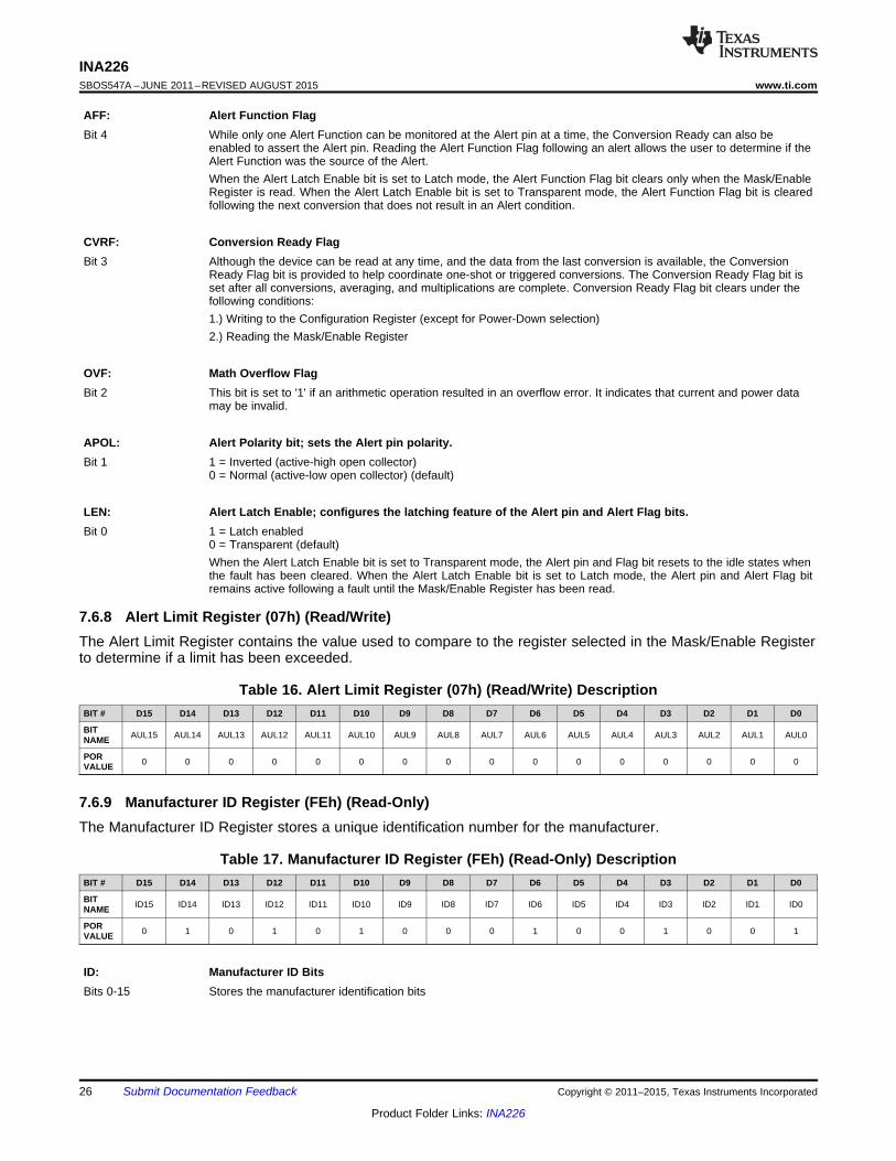
7.6.8 Alert Limit Register (07h) (Read/Write)The Alert Limit Register contains the value used to compare to the register selected in the Mask/Enable Registerto determine if a limit has been exceeded.
Table 16. Alert Limit Register (07h) (Read/Write) DescriptionBIT # D15 D14 D13 D12 D11 D10 D9 D8 D7 D6 D5 D4 D3 D2 D1 D0
BIT AUL15 AUL14 AUL13 AUL12 AUL11 AUL10 AUL9 AUL8 AUL7 AUL6 AUL5 AUL4 AUL3 AUL2 AUL1 AUL0NAME
POR 0 0 0 0 0 0 0 0 0 0 0 0 0 0 0 0VALUE
7.6.9 Manufacturer ID Register (FEh) (Read-Only)The Manufacturer ID Register stores a unique identification number for the manufacturer.
Table 17. Manufacturer ID Register (FEh) (Read-Only) DescriptionBIT # D15 D14 D13 D12 D11 D10 D9 D8 D7 D6 D5 D4 D3 D2 D1 D0
BIT ID15 ID14 ID13 ID12 ID11 ID10 ID9 ID8 ID7 ID6 ID5 ID4 ID3 ID2 ID1 ID0NAME
POR 0 1 0 1 0 1 0 0 0 1 0 0 1 0 0 1VALUE
ID: Manufacturer ID BitsBits 0-15 Stores the manufacturer identification bits
26 Submit Documentation Feedback Copyright © 2011–2015, Texas Instruments Incorporated
Product Folder Links: INA226

INA226www.ti.com SBOS547A –JUNE 2011–REVISED AUGUST 2015
7.6.10 Die ID Register (FFh) (Read-Only)The Die ID Register stores a unique identification number and the revision ID for the die.
Table 18. Die ID Register (FFh) (Read-Only) DescriptionBIT # D15 D14 D13 D12 D11 D10 D9 D8 D7 D6 D5 D4 D3 D2 D1 D0
BIT DID11 DID10 DID9 DID8 DID7 DID6 DID5 DID4 DID3 DID2 DID1 DID0 RID3 RID2 RID1 RID0NAME
POR 0 0 0 0 0 0 0 0 0 0 0 0 0 0 0 0VALUE
DID: Device ID BitsBits 4-15 Stores the device identification bits
RID: Die Revision ID BitsBit 0-3 Stores the device revision identification bits
Copyright © 2011–2015, Texas Instruments Incorporated Submit Documentation Feedback 27
Product Folder Links: INA226

´ Power Register
Current Register I C2
Interface
Voltage Register
GND
VBUS
ADC
V
I
A0
Alert
A1
SDA
SCL
C
0.1 µFBYPASS
10-ALoad
Alert Register
VS(Supply Voltage)
+12-V Supply
VIN-
VIN+
R
2 mSHUNT
W
Pullup Resistors
INA226SBOS547A –JUNE 2011–REVISED AUGUST 2015 www.ti.com
8 Application and Implementation
NOTEInformation in the following applications sections is not part of the TI componentspecification, and TI does not warrant its accuracy or completeness. TI’s customers areresponsible for determining suitability of components for their purposes. Validate and testthe design implementation to confirm system functionality.
8.1 Application InformationThe INA226 is a current shunt and power monitor with an I2C™ compatible interface. The device monitors both ashunt voltage drop and bus supply voltage. Programmable calibration value, conversion times, and averaging,combined with an internal multiplier, enable direct readouts of current in amperes and power in watts.
8.2 Typical Applications
8.2.1 High-Side Sensing Circuit Application
Figure 27. Typical Circuit Configuration, INA226
8.2.1.1 Design RequirementsINA226 measures the voltage developed across a current-sensing resistor (RSHUNT) when current passes throughit. The device also measures the bus supply voltage and can calculate power when calibrated. It comes with alertcapability where the alert pin can be programmed to respond to a user-defined event or to a conversion readynotification. This design illustrates the ability of the alert pin to respond to a set threshold.
28 Submit Documentation Feedback Copyright © 2011–2015, Texas Instruments Incorporated
Product Folder Links: INA226

Time (20 Ps/div)
D002
Ale
rt(2
V/d
iv)
Inpu
t/Lim
it(5
0 m
V/d
iv)
ALERTINPUTLIMIT
Time (200 Ps/div)
D002
Ale
rt(2
V/d
iv)
Inpu
t/Lim
it(5
0 m
V/d
iv)
ALERTINPUTLIMIT
INA226www.ti.com SBOS547A –JUNE 2011–REVISED AUGUST 2015
Typical Applications (continued)8.2.1.2 Detailed Design ProcedureThe Alert pin can be configured to respond to one of the five alert functions described in the Alert Pin section.The alert pin must to be pulled up to the VVS pin voltage via the pull-up resistors. The configuration register is setbased on the required conversion time and averaging. The Mask/Enable Register is set to identify the requiredalert function and the Alert Limit Register is set to the limit value used for comparison.
8.2.1.3 Application CurvesFigure 28 shows the Alert pin response to a shunt voltage over-limit of 80 mV for a conversion time (tCT) of 1.1ms and averaging set to 1. Figure 29 shows the response for the same limit but with the conversion time reducedto 140 µs.
See Table 19 tCT = 1.1 ms See Table 20 tCT = 140 µsSee Table 21 See Table 22 See Table 21 See Table 22
Figure 28. Alert Response Figure 29. Alert Response
Table 19. Configuration Register (00h) Settings for Figure 28 (Value = 4025h)BIT # D15 D14 D13 D12 D11 D10 D9 D8 D7 D6 D5 D4 D3 D2 D1 D0
BIT VBUSC VBUSC VBUSCRST — — — AVG2 AVG1 AVG0 VSHCT2 VSHCT1 VSHCT0 MODE3 MODE2 MODE1NAME T2 T1 T0
POR 0 1 0 0 0 0 0 0 0 0 1 0 0 1 0 1VALUE
Table 20. Configuration Register (00h) Settings for Figure 29 (Value = 4005h)BIT # D15 D14 D13 D12 D11 D10 D9 D8 D7 D6 D5 D4 D3 D2 D1 D0
BIT VBUSC VBUSC VBUSCRST — — — AVG2 AVG1 AVG0 VSHCT2 VSHCT1 VSHCT0 MODE3 MODE2 MODE1NAME T2 T1 T0
POR 0 1 0 0 0 0 0 0 0 0 0 0 0 1 0 1VALUE
Table 21. Mask/Enable Register (06h) Settings for Figure 28 and Figure 29 (Value = 8000h)BIT # D15 D14 D13 D12 D11 D10 D9 D8 D7 D6 D5 D4 D3 D2 D1 D0
BIT SOL SUL BOL BUL POL CNVR — — — — — AFF CVRF OVF APOL LENNAME
POR 1 0 0 0 0 0 0 0 0 0 0 0 0 0 0 0VALUE
Table 22. Alert Limit Register (07h) Settings for Figure 28 and Figure 29 (Value = 7D00)BIT # D15 D14 D13 D12 D11 D10 D9 D8 D7 D6 D5 D4 D3 D2 D1 D0
BIT AUL15 AUL14 AUL13 AUL12 AUL11 AUL10 AUL9 AUL8 AUL7 AUL6 AUL5 AUL4 AUL3 AUL2 AUL1 AUL0NAME
POR 0 1 1 1 1 1 0 1 0 0 0 0 0 0 0 0VALUE
Copyright © 2011–2015, Texas Instruments Incorporated Submit Documentation Feedback 29
Product Folder Links: INA226

Supply bypass capacitor
A0
A1
SDA
Alert
IN+
IN±
GND
VBUS
SCL VS
(1)
I2C/SMBUS interface
Via to Ground Plane
Via to Power Plane
Alert output (Can be left floating if unused)
Sense/Shunt Resistor
INA226SBOS547A –JUNE 2011–REVISED AUGUST 2015 www.ti.com
9 Power Supply RecommendationsThe input circuitry of the device can accurately measure signals on common-mode voltages beyond its powersupply voltage, VVS. For example, the voltage applied to the VVS power supply terminal can be 5 V, whereas theload power-supply voltage being monitored (the common-mode voltage) can be as high as 36 V. Note also thatthe device can withstand the full 0-V to 36-V range at the input terminals, regardless of whether the device haspower applied or not.
Place the required power-supply bypass capacitors as close as possible to the supply and ground terminals ofthe device to ensure stability. A typical value for this supply bypass capacitor is 0.1 μF. Applications with noisy orhigh-impedance power supplies may require additional decoupling capacitors to reject power-supply noise.
10 Layout
10.1 Layout GuidelinesConnect the input pins (IN+ and IN-) to the sensing resistor using a Kelvin connection or a 4-wire connection.These connection techniques ensure that only the current-sensing resistor impedance is detected between theinput pins. Poor routing of the current-sensing resistor commonly results in additional resistance present betweenthe input pins. Given the very low ohmic value of the current-sensing resistor, any additional high-current carryingimpedance causes significant measurement errors. Place the power-supply bypass capacitor as close aspossible to the supply and ground pins.
10.2 Layout Example
(1) connect the VBUS pin to the power supply rail.
Figure 30. INA226 Layout Example
30 Submit Documentation Feedback Copyright © 2011–2015, Texas Instruments Incorporated
Product Folder Links: INA226

INA226www.ti.com SBOS547A –JUNE 2011–REVISED AUGUST 2015
11 Device and Documentation Support
11.1 Device Support
11.1.1 Development Support• INA226EVM Evaluation Board and Software Tutorial (SBOU113)
11.2 Community ResourcesThe following links connect to TI community resources. Linked contents are provided "AS IS" by the respectivecontributors. They do not constitute TI specifications and do not necessarily reflect TI's views; see TI's Terms ofUse.
TI E2E™ Online Community TI's Engineer-to-Engineer (E2E) Community. Created to foster collaborationamong engineers. At e2e.ti.com, you can ask questions, share knowledge, explore ideas and helpsolve problems with fellow engineers.
Design Support TI's Design Support Quickly find helpful E2E forums along with design support tools andcontact information for technical support.
11.3 TrademarksE2E is a trademark of Texas Instruments.I2C is a trademark of NXP Semiconductors.All other trademarks are the property of their respective owners.
11.4 Electrostatic Discharge CautionThese devices have limited built-in ESD protection. The leads should be shorted together or the device placed in conductive foamduring storage or handling to prevent electrostatic damage to the MOS gates.
11.5 GlossarySLYZ022 — TI Glossary.
This glossary lists and explains terms, acronyms, and definitions.
12 Mechanical, Packaging, and Orderable InformationThe following pages include mechanical, packaging, and orderable information. This information is the mostcurrent data available for the designated devices. This data is subject to change without notice and revision ofthis document. For browser-based versions of this data sheet, refer to the left-hand navigation.
Copyright © 2011–2015, Texas Instruments Incorporated Submit Documentation Feedback 31
Product Folder Links: INA226

PACKAGE OPTION ADDENDUM
www.ti.com 19-Sep-2014
Addendum-Page 1
PACKAGING INFORMATION
Orderable Device Status(1)
Package Type PackageDrawing
Pins PackageQty
Eco Plan(2)
Lead/Ball Finish(6)
MSL Peak Temp(3)
Op Temp (°C) Device Marking(4/5)
Samples
INA226AIDGSR ACTIVE VSSOP DGS 10 2500 Green (RoHS& no Sb/Br)
CU NIPDAUAG Level-2-260C-1 YEAR -40 to 125 226
INA226AIDGST ACTIVE VSSOP DGS 10 250 Green (RoHS& no Sb/Br)
CU NIPDAUAG Level-2-260C-1 YEAR -40 to 125 226
(1) The marketing status values are defined as follows:ACTIVE: Product device recommended for new designs.LIFEBUY: TI has announced that the device will be discontinued, and a lifetime-buy period is in effect.NRND: Not recommended for new designs. Device is in production to support existing customers, but TI does not recommend using this part in a new design.PREVIEW: Device has been announced but is not in production. Samples may or may not be available.OBSOLETE: TI has discontinued the production of the device.
(2) Eco Plan - The planned eco-friendly classification: Pb-Free (RoHS), Pb-Free (RoHS Exempt), or Green (RoHS & no Sb/Br) - please check http://www.ti.com/productcontent for the latest availabilityinformation and additional product content details.TBD: The Pb-Free/Green conversion plan has not been defined.Pb-Free (RoHS): TI's terms "Lead-Free" or "Pb-Free" mean semiconductor products that are compatible with the current RoHS requirements for all 6 substances, including the requirement thatlead not exceed 0.1% by weight in homogeneous materials. Where designed to be soldered at high temperatures, TI Pb-Free products are suitable for use in specified lead-free processes.Pb-Free (RoHS Exempt): This component has a RoHS exemption for either 1) lead-based flip-chip solder bumps used between the die and package, or 2) lead-based die adhesive used betweenthe die and leadframe. The component is otherwise considered Pb-Free (RoHS compatible) as defined above.Green (RoHS & no Sb/Br): TI defines "Green" to mean Pb-Free (RoHS compatible), and free of Bromine (Br) and Antimony (Sb) based flame retardants (Br or Sb do not exceed 0.1% by weightin homogeneous material)
(3) MSL, Peak Temp. - The Moisture Sensitivity Level rating according to the JEDEC industry standard classifications, and peak solder temperature.
(4) There may be additional marking, which relates to the logo, the lot trace code information, or the environmental category on the device.
(5) Multiple Device Markings will be inside parentheses. Only one Device Marking contained in parentheses and separated by a "~" will appear on a device. If a line is indented then it is a continuationof the previous line and the two combined represent the entire Device Marking for that device.
(6) Lead/Ball Finish - Orderable Devices may have multiple material finish options. Finish options are separated by a vertical ruled line. Lead/Ball Finish values may wrap to two lines if the finishvalue exceeds the maximum column width.
Important Information and Disclaimer:The information provided on this page represents TI's knowledge and belief as of the date that it is provided. TI bases its knowledge and belief on informationprovided by third parties, and makes no representation or warranty as to the accuracy of such information. Efforts are underway to better integrate information from third parties. TI has taken andcontinues to take reasonable steps to provide representative and accurate information but may not have conducted destructive testing or chemical analysis on incoming materials and chemicals.TI and TI suppliers consider certain information to be proprietary, and thus CAS numbers and other limited information may not be available for release.

PACKAGE OPTION ADDENDUM
www.ti.com 19-Sep-2014
Addendum-Page 2
In no event shall TI's liability arising out of such information exceed the total purchase price of the TI part(s) at issue in this document sold by TI to Customer on an annual basis.

TAPE AND REEL INFORMATION
*All dimensions are nominal
Device PackageType
PackageDrawing
Pins SPQ ReelDiameter
(mm)
ReelWidth
W1 (mm)
A0(mm)
B0(mm)
K0(mm)
P1(mm)
W(mm)
Pin1Quadrant
INA226AIDGSR VSSOP DGS 10 2500 330.0 12.4 5.3 3.4 1.4 8.0 12.0 Q1
INA226AIDGST VSSOP DGS 10 250 330.0 12.4 5.3 3.4 1.4 8.0 12.0 Q1
PACKAGE MATERIALS INFORMATION
www.ti.com 19-Sep-2014
Pack Materials-Page 1

*All dimensions are nominal
Device Package Type Package Drawing Pins SPQ Length (mm) Width (mm) Height (mm)
INA226AIDGSR VSSOP DGS 10 2500 366.0 364.0 50.0
INA226AIDGST VSSOP DGS 10 250 366.0 364.0 50.0
PACKAGE MATERIALS INFORMATION
www.ti.com 19-Sep-2014
Pack Materials-Page 2


IMPORTANT NOTICE
Texas Instruments Incorporated and its subsidiaries (TI) reserve the right to make corrections, enhancements, improvements and otherchanges to its semiconductor products and services per JESD46, latest issue, and to discontinue any product or service per JESD48, latestissue. Buyers should obtain the latest relevant information before placing orders and should verify that such information is current andcomplete. All semiconductor products (also referred to herein as “components”) are sold subject to TI’s terms and conditions of salesupplied at the time of order acknowledgment.TI warrants performance of its components to the specifications applicable at the time of sale, in accordance with the warranty in TI’s termsand conditions of sale of semiconductor products. Testing and other quality control techniques are used to the extent TI deems necessaryto support this warranty. Except where mandated by applicable law, testing of all parameters of each component is not necessarilyperformed.TI assumes no liability for applications assistance or the design of Buyers’ products. Buyers are responsible for their products andapplications using TI components. To minimize the risks associated with Buyers’ products and applications, Buyers should provideadequate design and operating safeguards.TI does not warrant or represent that any license, either express or implied, is granted under any patent right, copyright, mask work right, orother intellectual property right relating to any combination, machine, or process in which TI components or services are used. Informationpublished by TI regarding third-party products or services does not constitute a license to use such products or services or a warranty orendorsement thereof. Use of such information may require a license from a third party under the patents or other intellectual property of thethird party, or a license from TI under the patents or other intellectual property of TI.Reproduction of significant portions of TI information in TI data books or data sheets is permissible only if reproduction is without alterationand is accompanied by all associated warranties, conditions, limitations, and notices. TI is not responsible or liable for such altereddocumentation. Information of third parties may be subject to additional restrictions.Resale of TI components or services with statements different from or beyond the parameters stated by TI for that component or servicevoids all express and any implied warranties for the associated TI component or service and is an unfair and deceptive business practice.TI is not responsible or liable for any such statements.Buyer acknowledges and agrees that it is solely responsible for compliance with all legal, regulatory and safety-related requirementsconcerning its products, and any use of TI components in its applications, notwithstanding any applications-related information or supportthat may be provided by TI. Buyer represents and agrees that it has all the necessary expertise to create and implement safeguards whichanticipate dangerous consequences of failures, monitor failures and their consequences, lessen the likelihood of failures that might causeharm and take appropriate remedial actions. Buyer will fully indemnify TI and its representatives against any damages arising out of the useof any TI components in safety-critical applications.In some cases, TI components may be promoted specifically to facilitate safety-related applications. With such components, TI’s goal is tohelp enable customers to design and create their own end-product solutions that meet applicable functional safety standards andrequirements. Nonetheless, such components are subject to these terms.No TI components are authorized for use in FDA Class III (or similar life-critical medical equipment) unless authorized officers of the partieshave executed a special agreement specifically governing such use.Only those TI components which TI has specifically designated as military grade or “enhanced plastic” are designed and intended for use inmilitary/aerospace applications or environments. Buyer acknowledges and agrees that any military or aerospace use of TI componentswhich have not been so designated is solely at the Buyer's risk, and that Buyer is solely responsible for compliance with all legal andregulatory requirements in connection with such use.TI has specifically designated certain components as meeting ISO/TS16949 requirements, mainly for automotive use. In any case of use ofnon-designated products, TI will not be responsible for any failure to meet ISO/TS16949.
Products ApplicationsAudio www.ti.com/audio Automotive and Transportation www.ti.com/automotiveAmplifiers amplifier.ti.com Communications and Telecom www.ti.com/communicationsData Converters dataconverter.ti.com Computers and Peripherals www.ti.com/computersDLP® Products www.dlp.com Consumer Electronics www.ti.com/consumer-appsDSP dsp.ti.com Energy and Lighting www.ti.com/energyClocks and Timers www.ti.com/clocks Industrial www.ti.com/industrialInterface interface.ti.com Medical www.ti.com/medicalLogic logic.ti.com Security www.ti.com/securityPower Mgmt power.ti.com Space, Avionics and Defense www.ti.com/space-avionics-defenseMicrocontrollers microcontroller.ti.com Video and Imaging www.ti.com/videoRFID www.ti-rfid.comOMAP Applications Processors www.ti.com/omap TI E2E Community e2e.ti.comWireless Connectivity www.ti.com/wirelessconnectivity
Mailing Address: Texas Instruments, Post Office Box 655303, Dallas, Texas 75265Copyright © 2015, Texas Instruments Incorporated