In this lecture, we discuss how digital electronics has ...
21
1 In this lecture, we discuss how digital electronics has evolved over the years, from discrete logic to highly integrated circuits. For this module, the digital technology that we will be focusing on is called “Field Programmable Gate Arrays” or FPGAs. This lecture will introduce you to the idea of such digital devices, and in particular, you will learn about the particular device that you will be using for the Laboratory sessions using the DE10-Lite board provided to you through the Lab-in-a-Box.
Transcript of In this lecture, we discuss how digital electronics has ...

1
In this lecture, we discuss how digital electronics has evolved over the years, from discrete logic to highly integrated circuits. For this module, the digital technology that we will be focusing on is called “Field Programmable Gate Arrays” or FPGAs. This lecture will introduce you to the idea of such digital devices, and in particular, you will learn about the particular device that you will be using for the Laboratory sessions using the DE10-Lite board provided to you through the Lab-in-a-Box.

In the first year, you learned about the different ways of describing or specifying a digital circuit.
1. Schematic diagrams with gates – this method is the first thing you learned and it is easy to understand. However, as will be seen in Lecture 3, this is not necessarily the best way to specify a large digital system.
2. Boolean equations – this provides a formal way to express logical relationships between Boolean variables. Useful when designing on paper, but less useful in practice. In particular, we rarely use Boolean algebra to perform logic simplification in real-life!
3. Truth Tables – this is a universal way to describe the behaviour of a circuit and we continue to use this in datasheets or even in actual designs.
4. Timing diagrams – this is a useful way to explain behaviour of sequential circuits and is used in datasheets. However, not that useful as a method to specify a circuit in a CAD system.
5. Hardware Description Languages (HDLs) – you have already done a bit of this last year. HDL is the way that most digital designs are specified nowadays. For this course, we will be using Verilog HDL, which is one that is very closed to the C language. It is also used extensively for designing integrated circuits such as ASICs and other type of chips. It is also popular in North America and in Asia.
Another popular HDL is VHDL. I personally find VHDL too wordy (verbose). Finally, there are now emerging higher level languages such as OpenCL, which is an attempto make hardware design more like programming a computer. This topic is left to later years.
2

You have also learned about the various building blocks for digital electronics. 1. Primitive gates – We have the basic AND, OR, NAND, NOR, XOR and XNOR gates.2. Multiplexers MUXs – These are really useful component. Shown here is a 2-to-1 MUX with two data inputs and one select input. The output is one or the other depending on the select input (sel). We often put a number of these together to provide multiplexing function to a multi-bit data word (as shown here with two 3-bit numbers).3. Arithmetic circuits – Commonly found are adders and multipliers. Subtractor can be built from an adder if we use 2’s complement representation of signed integers.4. Encoders/Decoders – These two are related. Encoding is a logic module that reduces (encodes) a large number of bits and produces fewer output bits. Decoders are the opposite. Shown here is a 7-segment display decoder, where 4 input bits are decoded into 7 logic signals to drive the seven segments of the display. The encoder here is known as a priority encoder. It produces a 3-bit output showing where the first ‘1’ is encounters from the most-significant bit D7 to the least significant bit D0.5. Flipflops and Registers – These are the building blocks for all sequential circuits. As will be seen later, we really only use one type of flipflop – the D-FF.These are all important components that all digital circuit designers need to be familiar with. However, nowadays, we rarely design large digital systems at such low levels. Instead we generally try to express these building blocks in a more abstract manner in a hardware description language (as we will see in later lectures).In addition to these basic blocks, we also have memory devices and processor blocks. These are topics that we will cover towards the end of this module.
3

All digital circuits exhibit propagation delays. Here it shows the delay table for a “discrete logic” CMOS NAND gate. The delay could be in the region of nanoseconds. However, with the FPGA chips we use for this module, the internal “gate” propagation delay are in tens of picoseconds, which is much faster than discrete logic. As can be seen later, the “gates” inside the FPGA are also much more complex than a simple NAND gate. In fact, they are not gates at all!
Also note that propagation delay depends on the “cause” (input rising or falling, and on the gradient of the edges) and the “effect” (output rising or falling). Delay also depends on what are connected to the output (i.e. the loading). As can be seen in the example here, the rising edge A to falling edge X delay is lower than that of A falling to X rising.
Note that I use an arrow to indicate the cause (the blunt end) and the effect (the pointed end) in a timing diagram.
4

You learned about various types of flipflops (FFs) in the first year. In fact, all you need is the D-FF. With a D-FF, you can construct circuits to behave like various types of flipflops: Toggle (T-FF), set-reset (SR-FF) or a JK-FF.
Therefore in this course, we will ONLY use D-FF for everything. This is in fact what happens in practical designs.
We use the IEEE standards for the symbol here. C mean clock input, the number 1 is a numerical label (as clock 1). D is for data input, and 1D means this input is controlled by input 1. Q is the flipflop output.
5

Timing and delay parameters for flipflop is different from that with gates. Shown here is a D-FF that responses to a rising edge on the clock signal. A D-FF is like a camera, taking a “picture” from the scene (input is D). The clock input C1 is like the trigger on the camera – when pressed it samples the input and take a picture. The “cause” here is the rising edge of the CLOCK and the “effect” is the Q output sampling the D input, and keep the value until the next rising edge of the clock.
The delay here is from CLOCK rising edge to Q output changing. However, for the D-FF to work properly, there are two other timing parameters which are important: the setup time and the hold time. I will be talking about these in a later lecture.
6

Here is an example of a D-FF used in a ripple counter.
Q0 value is first inverted (represented by the triangle) and then used as D input on the next clock cycle. The flipflop is triggered on the FALLING edge of CLOCK. Therefore the Q output “TOGGLES” on each active edge of the clock (i.e. falling edge). Q0 is therefore changing at half the rate of CLOCK, hence this flipflop acts as a divide-by-2 circuit.
The Q0 signal is now used as clock input to the next D-FF. Hence Q1 is toggling at half the frequency of Q0. The circuit is effectively a binary counter.
This is a simple finite state machine (FSM) because it has 8 states which cycles through in a sequence. FSM will be covered in some later lectures in details and it is a very important topic in digital designs.
We then use the Q0 output as the clock input the next stage etc. Note that because the 2nd stage only starts to work once the first stage is completed, the propagation of effects “ripples” through the circuit – hence we call this a “ripple counter”.
This counter is also known as an asynchronous sequential circuit. It is “asynchronous” because the output signals are NOT synchronised to a single clock signal (since there are many clock signals), and “sequential” because its current output value (or state) depends on previous output values in the sequence.
7

The ripple counter is potentially slow. The delay between the active edge of the clock and the counter output giving the correct value is dependent on the number of flipflops in the circuit and therefore the size of the counter (i.e. how many stages) .
A far better approach is to use the flipflops TOGETHER as a group, and clock them using THE SAME CLOCK signal as shown here. The Logic Block is a combinatorial circuit which computes the next D value D2:0 from the current Q value Q2:0. (D has three bits D0, D1 and D2. We use the notation D2:0 to represent this.) The relationship between D and Q is simple: D2:0 = Q2:0 + 1.
Since the three output bits Q2:0 change within a fraction of a nanosecond of each other, this circuit is: 1) faster than the ripple counter; 2) the “delay” is constant instead of dependent on the size of the counter.
This circuit is known as a synchronous sequential circuit because its function is synchronous to a single clock signal. If you regard the Q2:0 output value as a state value, it follows a finite number of states in a defined sequence. Therefore it is also a form of Finite State Machine.
Note the notation with the arrows.
8

9
Last year you learned about implementing digital circuits using gates such as the one shown here. You can still buy this chip with FOUR NAND gates in one package and this is known as discrete logic. We generally do not use these any more. It is slow, expensive, consumes lots of energy and very hard to use.
Nevertheless, it is good to learn about NAND and NOR gates because, using De Morgan’s theorem, you could in theory design and implement an Intel i7 microprocessor using use two input NAND or NOR gates alone. NAND or NOR gates therefore could be regarded as the building block of all digital circuits. Similarly, you could in theory build a car using only basic Lego blocks. Unfortunately such a car would not be very good.

10
In early days of integrated circuits, designers started using rows of basic gates (shown as the dark stuff here arranged in rows). These are either completely customised (full-custom) or it is made with standard rows of gates but leaving the gates unconnected. For a specific design, the gates are connect through metal lines in the wiring channels. Therefore the customisation is only in the wiring metal layers and not the layers with transistors. This is known as “semi-custom” application-specific integrated circuits (ASICs).

11
Of course you can also customise everything – each transistor and each wiring connected in a full-custom manner. Here is the layout of Intel i7 microprocessor (with 4 cores). Designing such a circuit is very expensive, highly risky, and once designed, it cannot be changed easily.
Most applications in electronic industry cannot afford to embark on such a design. This drives the rise of the Field Programmable Gate Array.

12
So what is an FPGA? You came across the idea of Programmable Logic Device in the first year, where the user can program what the logic gate does (be it a NAND or NOR or some form of SUM-of-PRODUCT implementation) or an adder, you as a user, can “program” the chip to perform that logic function. Now we can add another layer of user programmability – you can program how these logic gates are connected together! In that way, we have a general programmable logic chip. Unlike the microprocessor where the program is just the instruction to fix digital hardware, here you can program the hardware itself!
The first FPGA was introduced by Xilinx in 1985. It has arrays of logic blocks which are programmable. It is surrounded by PROGRAMMABLE ROUTING RESOURCES, which allows the user to define the interconnections between the logic blocks. It also has lots of very flexible input and output circuits (programmable for TTL, CMOS and other interface standards).
Nowadays, there are two major players in the FPGA domain: Xilinx and Altera (now part of Intel). These two company dominate 90% of the FPGA market with roughly equal share.

13
Let us look inside an FPGA. Consider the logic block shown in blue in the last slide (Altera calls their logic block a Logic Element (LE)). Typically an LE consists of a 4-input Look-up Table (LUT) and a D-flipflop. Let us for now NOT to worry about how the 4-LUT is implemented internally. Just treat this as a 4-input combinatorial circuit which produces one output signal as shown here. The IMPORTANT characteristic is that the 4-LUT can be user defined (or programmable) to implement ANY 4-input Boolean function.As we will see later, the lookup table is actually implemented with a bunch of multiplexers.

14
The Logic Elements are surrounded by lots of routing wires and interconnection switches. Typically a signal wire to the Logic Block or Logic Element can be connected to any of these wiring channels through a programmable connection (essentially a digital switch). Xilinx FPGAs also have dedicated switch blocks shown here. Horizontal and vertical wires can be connected through such a switch block with programmable switches (for now, don’t worry how that’s done).
FPGAs have huge amount of these programmable resources and switches. Typically a very small percentage of these are being connected (i.e. ON) for a given application.
The main advantage and attraction of FPGA comes from the programmable interconnect – more so than the programmable logic.

15
Programming an FPGA is called “configuration”. In programming a computer or microprocessor, we send to the computer instruction codes as ‘1’s and ‘0’s. These are interpreted (or decoded) by the computer which will follow the instruction to perform tasks. The microprocessor needs to be fed these program codes continuously for it to function.
In FPGAs, you only need to configure the chip ONCE on power-up. You download to the chip a BITSTREAM (also bits in ‘1’s and ‘0’s), which determines the logic functions performed by the Logic Elements, and the interconnecting switches in order to connect the different LEs together to make up your circuit. Once the bitstream is received, the FPGA no longer needs to read the 1’s and 0’s again, very unlike a microprocessor which has to continually decoding the machine instructions. That’s why we say that we configure an FPGA (instead of programming an FPGA, although the two words are used interchangeably).
What happens when you configure an FPGA? Let us consider the 4-input LUTs circuit. This is typically implement using a tree of four layers of 2-input to 1-output multiplexers. The entire circuit is behaving like a 16-to-1 multiplexer using the 4 inputs ABCD as the control of the MUX tree. For example, if ABCD = 0000, then the top-most input of the MUX is routed to Y output.
In this way, ABCD forms the input columns of a truth table. For 4-inputs, the truth table has 16 entries. The output Y for each of the truth table entry corresponds to the input of the MUX. Configuration involves fixing the inputs to the 16-to-1 MUX by storing ‘1’ or ‘0’ in the registers R. Changing the 16 values stored, you can change to truth-table to anything you want.

16
To configure the programmable routing, let us look at how the routing circuit works. Take Xilinx SWITCH BLOCK circuit (green blocks in slide 7). This block controls the connections between four horizontal channels and four vertical channels. The diamond shaped block is a potential interconnect site. Inside the switch block circuit, there are 6 transistor switches which are initially all OFF (or open circuit).
The gate input of EACH switch is controlled by the output of a 1-bit register (e.g. a 1-bit D-FF). If the register stores a ‘1’, the routing transistor will have its gate driven high. Since the transistor is an nMOS transistor, it will become conducting. In this way, configuring the routing resources simply means that the correct ‘1’s and ‘0’s are stored in the registers that control these routing transistors.
As you would expect, typically an FPGA would have hundreds of thousands of these routing switches, most of these are OFF. Once programmed, the interconnections are made. The bold lines in the diagram above (after programming) shows the programmed connections.
Bitsteam information used for configuration purpose are usually stored on a flash memory chip, which is download to the FPGA during power-up – similar to “booting up a computer”. Once this is done, the FPGA is progammed to perform a specific user function (e.g. your design in the VERI experiment).
Alternatively you can send the bitstream to the FPGA via a computer connection to the chip. On the DE1-SOC board, it does both. Powerup DE1 will configure the Cyclone V FPGA chip to a “waiting” mode, which makes the DE1 board talk to the computer via the USB port while flashing the lights ON and OFF. You then send to the board a bitstream of your design via the USB port.

17
Let us now look at the FPGA that you will use for this course. The Intel/Altera MAX 10 FPGA uses the basic 4-input LUT architecture as discussed earlier. These are called Logic Elements or LEs (equivalent to Xilinx’s Configurable Logic Blocks or CLBs). The MAX 10 FPGA family devices can have 10k to 50k LEs in one chip. These are shown as light blue in the diagram. They are organized in groups called Logic Array Blocks (LABs) – see later.There are also blocks of memory (shown in purple) and multipliers (in brown). Note that the internal structure follows the traditional array style with rows and columns. Each column has the SAME type of circuit (i.e. all LEs or all multipliers).On the edge are lots of programmable I/Os. These can be configured for different logic standards, as input or output, have different current drive strengths and slew rates.There are multiple phase-locked loops (PLLs) used for generating internal clock signals.There is a analogue-to-digital converter block for interfacing to analogue signals. The internal flash memory blocks are used to store program codes for soft 32-bit processors called Nios II. Unlike some other FPGAs with inbuilt ARM process, which is a hard block, MAX 10’s Nios II processor is implemented with LEs. If it is not needed, the configurable logic can be used for other purposes.
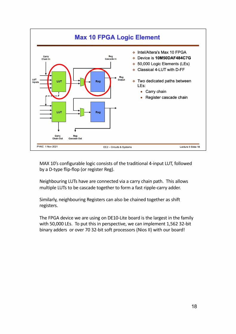
18
MAX 10’s configurable logic consists of the traditional 4-input LUT, followed by a D-type flip-flop (or register Reg).
Neighbouring LUTs have are connected via a carry chain path. This allows multiple LUTs to be cascade together to form a fast ripple-carry adder.
Similarly, neighbouring Registers can also be chained together as shift registers.
The FPGA device we are using on DE10-Lite board is the largest in the family with 50,000 LEs. To put this in perspective, we can implement 1,562 32-bit binary adders or over 70 32-bit soft processors (Nios II) with our board!

19
The Logic Elements are group into blocks of 16. Each block is known as Logic Array Block.
The reason for this approach (which is different from Xilinx’s switchboxes) is that most applications demand multiple bits working together. For example to implement a 16-bit counter, one would need 16 LEs. Most of the interconnections are local to these 16 LUTs and registers. Organising LEs in blocks of 16 with fast local connect is cheaper on routing resources and is faster in performance.
As shown here, the LABs are also connected to their neighbours in columns.

20
For this course, you will be designing circuits using the free version of the design suite known as Quartus Prime Lite from Intel/Altera.
This very powerful design tool contains everything you need to design a complex digital system ON YOUR OWN COMPUTER! You can download your copy from here: https://fpgasoftware.intel.com/18.0/?edition=lite&platform=windows
However, the software is only available for MS Windows or Linux operating system. If you are using a Mac, you would need to run a Virtual Machine applications (such as Virtual Box). A pre-configured Virtual Machine image is available for you to download and run under VirtualBox, which has Quartus pre-installed.
Beware that the software is very large – you need to have around 20 GB of free disk space. The minimum required RAM is 4GB, but 8GB is recommended.
Lab 3 provides full instructions on what you need to do have Quartus environment installed and set up.

21
This slide shows you the functional blocks of the Terasic DE10-Lite FPGA board that you are using for this module.
This has everything you need test basic designs involving switches, 7-segment displays and even a VGA output. We will be using this board for the remaining Lab Session for this module.