i.MX 8M Nano DDR4 EVK Board Hardware User's Guide · 2019-12-04 · Specifications i.MX 8M Nano...
16
© 2019 NXP B.V. i.MX 8M Nano DDR4 EVK Board Hardware User's Guide 1. Introduction This document is the hardware User’s Guide for the i.MX 8M Nano DDR4 Evaluation Kit (EVK) based on the NXP Semiconductor’s i.MX 8M Nano Applications Processor. This board is fully supported by NXP Semiconductor. This manual includes system setup and configurations, and provides detailed information on the overall design and usage of the EVK board from a hardware system perspective. 1.1. Board overview The DDR4 EVK board is a platform designed to show the most commonly used features of the i.MX 8M Nano Applications Processor. The i.MX 8M Nano DDR4 EVK board helps developers get familiar with the processor before investing a large amount of resources in more specific designs. Table 1 lists the features of the i.MX 8M Nano DDR4 EVK board. NXP Semiconductors Document Number: IMX8MNEVKHUG User's Guide Rev. 0 , 12/2019 Contents 1. Introduction........................................................................ 1 1.1. Board overview ....................................................... 1 1.2. Board contents ........................................................ 2 2. Specifications ..................................................................... 2 3. Processor ............................................................................ 5 3.1. Boot Mode and Boot Device configurations ........... 5 3.2. Power Tree .............................................................. 6 3.3. DDR4 DRAM memory ........................................... 8 3.4. eMMC memory (U4) .............................................. 9 3.5. QSPI Nor Flash (U5) .............................................. 9 3.6. SD card slot (J701) ................................................. 9 3.7. MIPI-CSI and MIPI-DSI connectors (J802, J801) .. 9 3.8. Ethernet connector (J501) ....................................... 9 3.9. USB connector (J301, J302) ................................... 9 3.10. Wi-Fi/Bluetooth (U6)............................................ 10 3.11. Audio Line output (J401) ...................................... 10 3.12. Audio Card connector (J1001) .............................. 10 3.13. JTAG connector (J902) ......................................... 10 3.14. USB-UART connector (J901) ............................... 11 3.15. Expansion connector (J1003) ................................ 11 3.16. I2C connector (J1004)........................................... 12 3.17. User interface buttons ........................................... 12 3.18. User interface LED indicators............................... 12 4. PCB information .............................................................. 14 4.1. EVK design files ................................................... 14 5. Revision history ............................................................... 15
Transcript of i.MX 8M Nano DDR4 EVK Board Hardware User's Guide · 2019-12-04 · Specifications i.MX 8M Nano...

© 2019 NXP B.V.
i.MX 8M Nano DDR4 EVK Board Hardware
User's Guide
1. Introduction
This document is the hardware User’s Guide for the
i.MX 8M Nano DDR4 Evaluation Kit (EVK) based on
the NXP Semiconductor’s i.MX 8M Nano Applications
Processor. This board is fully supported by NXP
Semiconductor. This manual includes system setup and
configurations, and provides detailed information on the
overall design and usage of the EVK board from a
hardware system perspective.
1.1. Board overview
The DDR4 EVK board is a platform designed to show
the most commonly used features of the i.MX 8M Nano
Applications Processor. The i.MX 8M Nano DDR4
EVK board helps developers get familiar with the
processor before investing a large amount of resources
in more specific designs.
Table 1 lists the features of the i.MX 8M Nano DDR4
EVK board.
NXP Semiconductors Document Number: IMX8MNEVKHUG
User's Guide Rev. 0 ,, 12/2019
Contents
1. Introduction ........................................................................ 1 1.1. Board overview ....................................................... 1 1.2. Board contents ........................................................ 2
2. Specifications ..................................................................... 2 3. Processor ............................................................................ 5
3.1. Boot Mode and Boot Device configurations ........... 5 3.2. Power Tree .............................................................. 6 3.3. DDR4 DRAM memory ........................................... 8 3.4. eMMC memory (U4) .............................................. 9 3.5. QSPI Nor Flash (U5) .............................................. 9 3.6. SD card slot (J701) ................................................. 9 3.7. MIPI-CSI and MIPI-DSI connectors (J802, J801) .. 9 3.8. Ethernet connector (J501) ....................................... 9 3.9. USB connector (J301, J302) ................................... 9 3.10. Wi-Fi/Bluetooth (U6)............................................ 10 3.11. Audio Line output (J401) ...................................... 10 3.12. Audio Card connector (J1001) .............................. 10 3.13. JTAG connector (J902) ......................................... 10 3.14. USB-UART connector (J901) ............................... 11 3.15. Expansion connector (J1003) ................................ 11 3.16. I2C connector (J1004)........................................... 12 3.17. User interface buttons ........................................... 12 3.18. User interface LED indicators ............................... 12
4. PCB information .............................................................. 14 4.1. EVK design files ................................................... 14
5. Revision history ............................................................... 15

Specifications
i.MX 8M Nano DDR4 EVK Board Hardware User's Guide, User's Guide, Rev. 0, 12/2019
2 NXP Semiconductors
Table 1. Board features
Processor NXP Applications Processor MIMX8MN6DVTJZAA
DRAM memory Micron 2 GB DDR4 MT40A1G16RC-062E:B
Mass storage SanDisk 16 GB eMMC5.1 SDINBDG4-16G-I1
Micron 32 MB QSPI NOR MT25QU256ABA1EW7-0SIT
MicroSD card connector SD3.0 supported
Power ROHM PMIC BD71850 + Discrete DCDC/LDO
Camera CSI interface (Mini-SAS connector)
Display interface DSI interface (Mini-SAS connector)
Ethernet 1 GB Ethernet with RJ45 connector
USB Port1 is USB (2.0) Type-C connector, Port2 is used as the Power Input
Wi-Fi/Bluetooth x1 on board Wi-Fi/Bluetooth module, 802.11a/b/g/n/ac, BT5.0
Audio connectors 3.5 mm Stereo Line output, 2Vrms
FPC connector (SAI ports) for Audio Card
Debug connectors JTAG (10pin header)
MicroUSB for UART debug, two COM Ports for A53 and M7
Expansion connector 40-pin dual-row Pin Header for I2S, UART, I2C and GPIO expansion
I2C connector 8-pin dual-row Pin Header for I2C expansion
Buttons ON/OFF, RESET
LED indicators Power status, UART
PCB 8MNANOD4-CPU: 2inch x 2inch, 6-layer
8MMINI-BB: 4inch x 4.2inch, 8-layer
Orderable part number 8MNANOD4-EVK
*consists of 8MNANOD4-CPU plus 8MMINI-BB, boards not orderable separately
1.2. Board contents
The i.MX 8M Nano DDR4 EVK contains the following items:
• i.MX 8M Nano DDR4 EVK board, assembled by two separate boards, 8MNANOD4-CPU
(SOM Board) and 8MMINI-BB (Base Board)
• IMX-MIPI-HDMI Accessory Card, MIPI-DSI to HDMI adapter board
• USB Type-C 45W Power Delivery Supply, 5V/3A, 9V/3A, 15V/3A, 20V/2.25A supported
• Mini-SAS cable, 8" mini-SAS cable
• USB Type-C Cable, Cable – Assembly, USB 3.0, Type-C Male to Type-A Male
• USB micro-B Cable, Cable – Assembly, USB 2.0, Type-A Male to Micro-B Male
• USB Type-C to A Adapter, Adapter – USB 3.0, Type-C Male to Type-A Female
• Quick Start Guide
2. Specifications
This section provides the detailed information about the electrical design and practical considerations on
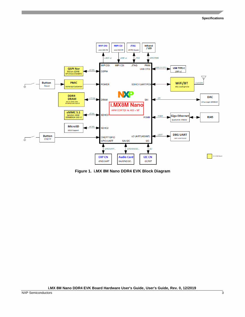
the DDR4 EVK board. Figure 1 describes each block in the high-level block diagram of the DDR4
EVK board.
Specifications
i.MX 8M Nano DDR4 EVK Board Hardware User's Guide, User's Guide, Rev. 0, 12/2019
NXP Semiconductors 3
Figure 1. i.MX 8M Nano DDR4 EVK Block Diagram

Specifications
i.MX 8M Nano DDR4 EVK Board Hardware User's Guide, User's Guide, Rev. 0, 12/2019
4 NXP Semiconductors
Figure 2 shows the overview of the i.MX 8M Nano DDR4 EVK board.
Figure 2. i.MX 8M Nano DDR4 EVK board overview
CAUTION
Type-C Port2 is the only power supply port, and it must be always supplied for system
running.
i.MX 8M Nano EVK is not a typical use case of the PD device. It is supplied by the
PD charger only, but with a power switch. When the switch keeps OFF for more than
5.5 seconds after adapting the PD charger, the charger (Source) will repower EVK
(Sink) after the system initiates the PD software. See Section 6.5.7 in the Universal
Serial Bus Power Delivery Specification Revision 2.0. There are two ways to avoid
repower:
• The power switch must always be in the ON position before attaching the PD
charger.
• Change the software to disable the PD function, and make it Type-C supply
only.
8MNANOD4-CPU
8MMINI-BB

Specifications
i.MX 8M Nano DDR4 EVK Board Hardware User's Guide, User's Guide, Rev. 0, 12/2019
NXP Semiconductors 5
3. Processor
The i.MX 8M Nano applications processors represent NXP Semiconductor’s latest achievement in
highly integrated multimedia-focused products offering high performance processing. These
applications processors can enable the growing market of smart, secure, connected devices. The i.MX
8M Nano applications processors feature NXP’s advanced implementation of the Quad Arm Cortex®-
A53+ Arm Cortex®-M7 cores, which operate at speeds up to 1.5 GHz and 650 MHz respectively. Each
i.MX 8M Nano device provides a 16-bit DDR3L/DDR4/LPDDR4 memory interface and other interfaces
for connecting peripherals, such as MIPI LCD, MIPI Camera, WLAN, Bluetooth™, Ethernet, Digital
Mic, and multi-sensors.
For more detailed information about the processor, see the datasheet and reference manual on
www.nxp.com/i.MX8MNANO.
3.1. Boot Mode and Boot Device configurations
The i.MX 8M Nano implement a compressed boot mode decode with four BOOT_MODE pins. It can
boot from the boot configuration selected on SW1101 or from the boot configuration stored on the
internal eFUSE. In addition, the i.MX 8M Nano can download a program image from a USB connection
when configured in serial downloader mode. The method used to determine where the processor finds its
boot information is from four dedicated BOOT MODE pins.
On the i.MX 8M Nano DDR4 EVK board, the default boot mode is to boot from the eMMC device.
There are two additional boot devices; a QSPI Nor Flash on the CPU board, and a MicroSD connector
on the Base Board. If you set the boot device to QSPI or MicroSD, the board will boot from the device
accordingly.
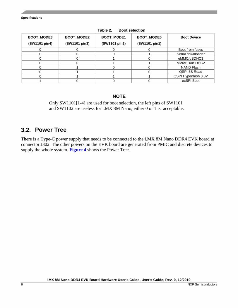
Table 2 shows the values used for boot selection.
Figure 3. Boot Selection
Specifications
i.MX 8M Nano DDR4 EVK Board Hardware User's Guide, User's Guide, Rev. 0, 12/2019
6 NXP Semiconductors
Table 2. Boot selection
BOOT_MODE3
(SW1101 pin4)
BOOT_MODE2
(SW1101 pin3)
BOOT_MODE1
(SW1101 pin2)
BOOT_MODE0
(SW1101 pin1)
Boot Device
0 0 0 0 Boot from fuses
0 0 0 1 Serial downloader
0 0 1 0 eMMC/uSDHC3
0 0 1 1 MicroSD/uSDHC2
0 1 0 0 NAND Flash
0 1 1 0 QSPI 3B Read 0 1 1 1 QSPI Hyperflash 3.3V 1 0 0 0 ecSPI Boot
NOTE
Only SW1101[1-4] are used for boot selection, the left pins of SW1101
and SW1102 are useless for i.MX 8M Nano, either 0 or 1 is acceptable.
3.2. Power Tree
There is a Type-C power supply that needs to be connected to the i.MX 8M Nano DDR4 EVK board at
connector J302. The other powers on the EVK board are generated from PMIC and discrete devices to
supply the whole system. Figure 4 shows the Power Tree.

Specifications
i.MX 8M Nano DDR4 EVK Board Hardware User's Guide, User's Guide, Rev. 0, 12/2019
NXP Semiconductors 7
1010----26002200300500NxCxVx(0.5xF)NxCxVx(0.5xF)10010--10
5V [400mA-3400mA]
5V/5A
LDO
Port2
VBUS_INSEQ
DCDC BUCK
ADP191ACBZ-R7
5V/3A
VCC
3.3V
DCDC BUCK
SEQ
AVDD/LINE VDD
QSPI
mini-SAS (MIPI CSI/DSI)
LDO1LDO2RTC_RESET_BRTC_CLKBUCK1BUCK2LDO3BUCK7BUCK8BUCK6MUXSWLDO6POR_B
1.80.8----0.85/0.950.85/0.95/1.01.81.81.23.33.3/1.81.2--1.8/2.5
USB TYPE-C
5-20V
DCDC_5V
2.5V/300mA
VDDEXT_3V3
TYP
Power SW
MPS MP8759GD
USB Type-C
2500mA
VCCQVCC
CPU: i.MX8M Nano
WiFi/BT
TYP
VCC
VDD_5V
MPS MP2147
LPDDR4
MicroSD
NVCC_SNVS_1V8VDD_SNVS_0V8RTC_RESET_BCLK_32K_OUTVDD_SOC&DRAM&PU_0V9VDD_ARM_0V9VDDA_1V8VDD_1V8/NVCC_1V8NVCC_DRAM_1V2NVCC_3V3NVCC_SD2VDD_PHY_1V2POR_BNVCC_ENET
PMIC: BD71850
Load SW
1.80.8----0.85/0.950.85/0.95/1.01.81.81.1 → 1.23.33.3/1.81.2--
8MNANOD4-EVK PWR TREE
3000mA
MOSFET
3.3V/4A
RT9193-25GB
Required(mA)PWR/Signal
DRP PD (5-20V)
VSYS
VBATVIO
123456678991011
VPPVDD/VDDQ
Max Capability(mA)
1.8V3.3V5V
5V/3A
eMMC
REG
M.2 PCIe
1010----30003000300150030003000150300--
Audio DAC
123456678991011
Figure 4. Power Tree Diagram
In Figure 4, the developer can get all the voltage supply rails used on the EVK board. When some
modules are not enabled, the power supplies might be shut down by software. Table 3 lists the power
rails on the board.

Specifications
i.MX 8M Nano DDR4 EVK Board Hardware User's Guide, User's Guide, Rev. 0, 12/2019
8 NXP Semiconductors
Table 3. Power rails
SEQ Power Rail Regulator Value/V
0 DCDC_5V Discrete 5
1 NVCC_SNVS_1V8 BD71850 LDO1 1.8
2 VDD_SNVS_0V8 BD71850 LDO2 0.8
3 RTC_RESET_B BD71850 -
4 CLK_32K_OUT BD71850 -
5 VDD_SOC_DRAM_PU_0V9 BD71850 BUCK1 0.85/0.951
6 VDD_ARM_0V9 BD71850 BUCK2 0.85/0.95/1.02
6 VDDA_1V8 BD71850 LDO3 1.8
7 VDD_1V8/NVCC_1V8 BD71850 BUCK7 1.8
8 NVCC_DRAM_1V2 BD71850 BUCK8 1.23
9 VDD_3V3/NVCC_3V3 BD71850 BUCK6 3.3
9 NVCC_SD2 BD71850 MUXSW 3.3/1.8
9 VDD_5V Load Switch 5
9 VDDEXT_3V3 Discrete 3.3
10 VDD_PHY_1V2 BD71850 LDO6 1.2
11 POR_B BD71850 -
12 VSD_3V3 Load Switch 3.3
1. BD71850 BUCK1 default output voltage is 0.8 V. Software will change it to 0.85 V for nominal mode, 0.95 V for overdrive mode in SPL before DDR initialization.
2. BD71850 BUCK2 default output voltage is 0.9 V. Software will change it to 0.85 V for 1.2 GHz operation, 0.95 V for 1.4 GHz, 1.0 V for 1.5 GHz.
3. BD71850 BUCK8 default output voltage is 1.1 V. Software will change it to 1.2 V in SPL before DDR initialization.
3.3. DDR4 DRAM memory
The i.MX 8M Nano DDR4 EVK board has one 1G x 16 (1 channel x 16 I/O) DDR4 SDRAM chip
(MT40A1G16RC-062E:B) for a total of 2 GB RAM memory.
In the physical layout, the DDR4 chip is placed on the TOP side, the data traces are not necessarily
connected to the DDR4 chips in sequential order, but for ease of routing, are connected as best
determined by the layout and other critical traces.
The DRAM_VREF can be generated by i.MX 8M Nano internally, so it does not need to use external
power supply and decoupling capacitors. The calibration resistors used by the DDR4 chips and
processor are 240 Ohm 1 % resistors. The differential termination resistors for DRAM Clock are two 43
ohm 1 % with one 0.22 uF capacitance on EVK. Developers can change this value depending on
simulation and test result.

Specifications
i.MX 8M Nano DDR4 EVK Board Hardware User's Guide, User's Guide, Rev. 0, 12/2019
NXP Semiconductors 9
3.4. eMMC memory (U4)
The eMMC memory is connected to the uSDHC3 interface of i.MX 8M Nano, and it can support up to
eMMC 5.1 device. The eMMC memory is on the 8MNANOD4-CPU board, and the part number is
SDINBDG4-16G-I1. It is the default boot device of the EVK. The boot settings are as shown in Table 2.
3.5. QSPI Nor Flash (U5)
The QSPI memory is connected to the FlexSPI interface of i.MX 8M Nano, and it can support up to
166 MHz DDR mode device. The QSPI memory is on the 8MNANOPD4-CPU board, and the part
number is MT25QU256ABA1EW7-0SIT. To select it as the boot device of the EVK, developers can
refer to the boot settings as shown in Table 2.
3.6. SD card slot (J701)
There is one MicroSD card slot (J701) on the 8MMINI-BB board, connecting to the uSDHC2 interface
of i.MX 8M Nano. This connector supports one 4-bit SD3.0 MicroSD card. To select it as the boot
device of the EVK, developers can refer to the boot settings as shown in Table 2.
3.7. MIPI-CSI and MIPI-DSI connectors (J802, J801)
The i.MX 8M Nano processor supports one 4-lane MIPI-CSI and one 4-lane MIPI-DSI. The MiniSAS
connectors are designed to support camera and LCD with dedicated pin definition. The connectors are as
shown in Figure 2. Display and camera accessory boards are available separately. The full list can be
found at www.nxp.com/i.MX8-ACCESSORY-BOARDS.
3.8. Ethernet connector (J501)
The Ethernet subsystem of the EVK board is provided by the Qualcomm AR8031 Ethernet Transceiver
(U501). The Ethernet Transceiver (or PHY) receives standard RGMII Ethernet signals from the MAC-
NET core of the i.MX 8M Nano. The processor handles all Ethernet protocols at the MAC layer and
above. The PHY is only responsible for the Link Layer formatting. The Ethernet connector (J501)
integrates Magnetic transformer inside, so it cannot be directly connected to AR8031 (U501).
Each EVK board has a unique MAC address, which is burned into i.MX 8M Nano by Fuse. A label with
the unique MAC address is placed on the connector for reference.
3.9. USB connector (J301, J302)
The i.MX 8M Nano Applications Processors contain one USB 2.0 OTG controller, with one integrated
USB PHY. There are two USB Type-C connectors on the EVK board, but only Port1 can support Host
and Device Mode.
J301 is connected to USB1 interface of i.MX 8M Nano, which can act as the download port of the EVK.
Specifications
i.MX 8M Nano DDR4 EVK Board Hardware User's Guide, User's Guide, Rev. 0, 12/2019
10 NXP Semiconductors
J302 is the power supply port of the EVK.
3.10. Wi-Fi/Bluetooth (U6)
The EVK board has a Wi-Fi/Bluetooth module LBEE5HY1MW on the 8MNANOD4-CPU board. The
module is Cypress CYW43455 based, contains SDIO3.0, UART, PCM interface, and can support
802.11a/b/g/n/ac, BT5.0. The 2.4G/5G antenna is stuck to the edge of the Base Board with a coaxial
cable connected to the CPU Board.
3.11. Audio Line output (J401)
The EVK board uses a high-quality Stereo DAC WM8524 (U401), which can support 24 bit I2S data
and 192 KHz sampling rate. The Line output of WM8524 is 2Vrms, not like common headphone output
1 Vrms. Developers must be very careful about this interface. The Line output connector (J401) is a
3.5 mm 4-pole (or TRRS) phone jack.
CAUTION
The Audio Line output connector is designed for active speaker with a power amplifier. To connect it with a
headphone, make sure that the headphone has volume control functionality and set the headphone’s volume
properly before wearing it. Do not plug in the non-volume-control headphone directly. The audio output
volume may be too high for non-volume-control headphone and may damage it.
3.12. Audio Card connector (J1001)
One 60-pin FPC connector (J1001) is provided on the EVK board to support audio card connection, and
the developers can use the audio card to perform audio features development.
CAUTION
There is no SAI1 from the i.MX 8M Nano process, so AK4458/ AK4497 can’t be enabled on audio card.
3.13. JTAG connector (J902)
The i.MX 8M Nano Applications Processor has four JATG signals on dedicated pins, and one HW reset
input signal POR_B. Those signals are directly connected to the 10-pin 1.27 mm JTAG connector J902.
The four JTAG signals used by the processor are:
• JTAG_TCK TAP Clock
• JTAG_TMS TAP Machine State
• JTAG_TDI TAP Data In
• JTAG_TDO TAP Data Out

Specifications
i.MX 8M Nano DDR4 EVK Board Hardware User's Guide, User's Guide, Rev. 0, 12/2019
NXP Semiconductors 11
3.14. USB-UART connector (J901)
The i.MX 8M Nano Applications Processor has four independent UART Ports (UART1 – UART4). On
the EVK board, UART2 is used for Cortex-A53 core, and UART4 is used for Cortex-M7 core. We use a
Single chip USB to dual channel UART IC for system debugging, and the part number is FT2232D. The
developers can download the driver from FTDI website http://www.ftdichip.com/Drivers/VCP.htm.
After the driver for FT2232D is installed, the PC will enumerate two COM ports when the USB cable is
plugged into J901. Developers can use Putty, Tera Term, Xshell, or other terminal tools. The required
settings are as listed in Table 4.
Table 4. Terminal setting parameters
Data Rate 115,200 Baud
Data bits 8
Parity None
Stop bits 1
3.15. Expansion connector (J1003)
One 40-pin dual-row Pin Header connector (J1003) is provided on the EVK board to support I2S,
UART, I2C, and GPIO connection. The developers can use the port for some specific application
development.
Table 5. J1003 Pin Definition
Num Net Name Description Num Net Name Description
1 VEXT_3V3 Power Output, 3.3V 2 VDD_5V Power Output, 5V
3 I2C3_SDA_3V3 I2C3 data signal 4 VDD_5V Power Output, 5V
5 I2C3_SCL_3V3 I2C3 clock signal 6 GND Ground
7 UART3_CTS UART3 clear to send signal 8 UART3_TXD UART3 transmit signal
9 GND Ground 10 UART3_RXD UART3 transmit signal
11 UART3_RTS UART3 request to send signal 12 EXP_IO8 Expansion IO signal
13 EXP_IO9 Expansion IO signal 14 GND Ground
15 EXP_IO10 Expansion IO signal 16 EXP_IO11 Expansion IO signal
17 VEXT_3V3 Power Output, 3.3V 18 - NC
19 ECSPI2_MOSI SPI2 data signal, master
output slave input
20 GND Ground
21 ECSPI2_MISO SPI2 data signal, master input
slave output
22 - NC
23 ECSPI2_SCLK SPI2 clock signal 24 ECSPI2_SS0 SPI2 chip select signal
25 GND Ground 26 - NC
27 - NC 28 - NC
29 - NC 30 GND Ground
31 EXP_IO14 Expansion IO signal 32 EXP_IO12 Expansion IO signal
33 EXP_IO13 Expansion IO signal 34 GND Ground
35 SAI5_RXD3 SAI5 receive data signal 36 SAI5_RXD2 SAI5 receive data signal
37 SAI5_RXD1 SAI5 receive data signal 38 SAI5_RXD0 SAI5 receive data signal
39 GND Ground 40 SAI5_RXC SAI5 receive clock signal

Specifications
i.MX 8M Nano DDR4 EVK Board Hardware User's Guide, User's Guide, Rev. 0, 12/2019
12 NXP Semiconductors
3.16. I2C connector (J1004)
One 8-pin dual-row Pin Header connector (J1004) is provided on the EVK board to support I2C
connection. The developers can use the port for some specific application development.
Table 6. J1004 Pin Definition
Num Net Name Description
1/2 VDD_3V3 Power Output, 3.3V
3/4 I2C3_SCL_3V3 I2C clock signal
5/6 I2C3_SDA_3V3 I2C data signal
7/8 GND Ground
3.17. User interface buttons
There are two user interface buttons on the EVK board.
3.17.1. Power button (SW901)
The i.MX 8M Nano Applications Processor supports the use of a button input signal to request main
SoC power state changes (i.e. ON or OFF) from the PMU.
The ON/OFF button can be used for debounce, OFF-to-ON time, and max timeout. Debounce is used to
generate the power-off interrupt. In the ON state, if ON/OFF button is held longer than the debounce
time, the power-off interrupt is generated. In the OFF state, if the ON/OFF button is held longer than the
OFF-to-ON time, the state will transit from OFF to ON. Max timeout can also be the time for requesting
physical power down after the ON/OFF button has been held for the defined time.
3.17.2. Reset button (SW902)
The RESET button (SW902) is directly connected to the PMIC BD71850. Holding the RESET button
will force to reset the PMIC power outputs except NVCC_SNVS_1V8 and VDD_SNVS_0V8 on the
EVK board. The i.MX 8M Nano applications processor will be immediately turned off and reinitiate a
boot cycle from the OFF state.
3.18. User interface LED indicators
There are four LED indicators on the board. These LEDs have the following functions:
• Main Power Supply (D708)
— Green – The board is powered on.
— OFF – The board is powered off.
• System Status (D1) on 8MNANOD4-CPU
— Green Blinking – CPU is running well.
— OFF – CPU is not running.

Specifications
i.MX 8M Nano DDR4 EVK Board Hardware User's Guide, User's Guide, Rev. 0, 12/2019
NXP Semiconductors 13
• M7 UART (D902/D903)
— D902 Green light flashing – The UART data transmitted to PC.
— D903 Orange light flashing – The UART data received from PC.
• A53 UART (D906/D905)
— D906 Green light flashing – The UART data transmitted to PC.
— D905 Orange light flashing – The UART data received from PC.
Figure 5. LED indicator
D708 D905 D906 D902 D903
D1
Specifications
i.MX 8M Nano DDR4 EVK Board Hardware User's Guide, User's Guide, Rev. 0, 12/2019
14 NXP Semiconductors
4. PCB information
The i.MX 8M Nano DDR4 EVK is composed by 8MNANOD4-CPU and 8MMINI-BB. Table 1 lists the
dimensions of the two boards. Both the two boards are made with standard 8-layer technology. The
material is FR-4, and the PCB stack-up information is shown in Table 7 and Table 8.
Table 7. 8MNANOD4-CPU Board stack up information
Layer Description Coppoer (Oz.) Dielectric thickness (mil)
1 Signal 0.5+Plating
Dielectric 2.76 mil
2 GND 1
Dielectric 2.95 mil
3 Signal 1
Dielectric 25.28 mil
5 Power 1
Dielectric 2.95 mil
6 Power 1
Dielectric 2.76 mil
8 Signal 0.5+Plating
Total thickness: 47.24(4.72/-4.72) mil 1.2(+0.12/-0.12) MM
Material: TU768 TU768
Table 8. 8MMINI-BB Board stack up information
Layer Description Coppoer (Oz.) Dielectric thickness (mil)
1 Signal 0.5+Plating
Dielectric 2.717 mil
2 GND 1
Dielectric 4.33 mil
3 Signal 1
Dielectric 11.085 mil
4 Power 1
Dielectric 14.170 mil
5 Power 1
Dielectric 11.415 mil
6 Signal 1
Dielectric 4.33 mil
7 GND 1
Dielectric 2.717 mil
8 Signal 0.5+Plating
Total thickness: 62.992(6.299/-6.299) mil 1.6(+0.16/-0.16) MM
Material: TU768 TU768
4.1. EVK design files
You can download the schematics, layout files, gerber files, and BOM from
www.nxp.com/imx8mnanoevk.

Specifications
i.MX 8M Nano DDR4 EVK Board Hardware User's Guide, User's Guide, Rev. 0, 12/2019
NXP Semiconductors 15
5. Revision history Table 9. Revision history
Revision number Date Substantive changes
0 12/2019 Initial release.

Document Number: IMX8MNEVKHUG Rev. 0
12/2019
How to Reach Us:
Home Page:
www.nxp.com/
Web Support:
www.nxp.com/support
Information in this document is provided solely to enable system and software implementers
to use NXP products. There are no express or implied copyright licenses granted hereunder
to design or fabricate any integrated circuits based on the information in this document. NXP
reserves the right to make changes without further notice to any products herein.
NXP makes no warranty, representation, or guarantee regarding the suitability of its products
for any particular purpose, nor does NXP assume any liability arising out of the application or
use of any product or circuit, and specifically disclaims any and all liability, including without
limitation consequential or incidental damages. “Typical” parameters that may be provided in
NXP data sheets and/or specifications can and do vary in different applications, and actual
performance may vary over time. All operating parameters, including “typicals,” must be
validated for each customer application by customer's technical experts. NXP does not
convey any license under its patent rights nor the rights of others. NXP sells products
pursuant to standard terms and conditions of sale, which can be found at the following
address: nxp.com/SalesTermsandConditions.
While NXP has implemented advanced security features, all products may be subject to
unidentified vulnerabilities. Customers are responsible for the design and operation of their
applications and products to reduce the effect of these vulnerabilities on customer’s
applications and products, and NXP accepts no liability for any vulnerability that is
discovered. Customers should implement appropriate design and operating safeguards to
minimize the risks associated with their applications and products.
NXP, NXP, the NXP logo, NXP SECURE CONNECTIONS FOR A SMARTER WORLD,
COOLFLUX, EMBRACE, GREENCHIP, HITAG, I2C BUS, ICODE, JCOP, LIFE VIBES,
MIFARE, MIFARE CLASSIC, MIFARE DESFire, MIFARE PLUS, MIFARE FLEX, MANTIS,
MIFARE ULTRALIGHT, MIFARE4MOBILE, MIGLO, NTAG, ROADLINK, SMARTLX,
SMARTMX, STARPLUG, TOPFET, TRENCHMOS, UCODE, Freescale, the Freescale logo,
AltiVec, C-5, CodeTEST, CodeWarrior, ColdFire, ColdFire+, C-Ware, the Energy Efficient
Solutions logo, Kinetis, Layerscape, MagniV, mobileGT, PEG, PowerQUICC, Processor
Expert, QorIQ, QorIQ Qonverge, Ready Play, SafeAssure, the SafeAssure logo, StarCore,
Symphony, VortiQa, Vybrid, Airfast, BeeKit, BeeStack, CoreNet, Flexis, MXC, Platform in a
Package, QUICC Engine, SMARTMOS, Tower, TurboLink, and UMEMS,EdgeScale,
EdgeLock, eIQ, and Immersive 3D are trademarks of NXP B.V. All other product or service
names are the property of their respective owners. Arm, AMBA, Arm Powered, Artisan,
Cortex, Jazelle, Keil, SecurCore, Thumb, TrustZone, and μVision are registered trademarks
of Arm Limited (or its subsidiaries) in the EU and/or elsewhere. Arm7, Arm9, Arm11,
big.LITTLE, CoreLink, CoreSight, DesignStart, Mali, Mbed, NEON, POP, Sensinode,
Socrates, ULINK and Versatile are trademarks of Arm Limited (or its subsidiaries) in the EU
and/or elsewhere. All rights reserved. Oracle and Java are registered trademarks of Oracle
and/or its affiliates. The Power Architecture and Power.org word marks and the Power and
Power.org logos and related marks are trademarks and service marks licensed by
Power.org.
© 2019 NXP B.V.