
PE29102 Evaluation Kit (EVK) User’s Manual - pSemi – (10/2017) EVK User’s Manual PE29102...
30
DOC-82956-3 – (10/2017) EVK User’s Manual www.psemi.com PE29102 Evaluation Kit (EVK) User’s Manual EK29102-03 EVK User’s Manual
Transcript of PE29102 Evaluation Kit (EVK) User’s Manual - pSemi – (10/2017) EVK User’s Manual PE29102...

DOC-82956-3 – (10/2017) EVK User’s Manualwww.psemi.com
PE29102 Evaluation Kit (EVK) User’s ManualEK29102-03 EVK User’s Manual

PE29102EK29102-03 EVK User’s Manual
Page ii DOC-82956-3 – (10/2017)www.psemi.com
Copyright and Trademarks©2017, Peregrine Semiconductor Corporation. All rights reserved. The Peregrine name, logo, UTSi and UltraCMOS are registered trademarks and HaRP, MultiSwitch and DuNE are trademarks of Peregrine Semiconductor Corp.
DisclaimersThe information in this document is believed to be reliable. However, Peregrine assumes no liability for the use of this information. Use shall be entirely at the user’s own risk. No patent rights or licenses to any circuits described in this document are implied or granted to any third party. Peregrine’s products are not designed or intended for use in devices or systems intended for surgical implant, or in other applications intended to support or sustain life, or in any application in which the failure of the Peregrine product could create a situation in which personal injury or death might occur. Peregrine assumes no liability for damages, including consequential or incidental damages, arising out of the use of its products in such applications.
Patent StatementPeregrine products are protected under one or more of the following U.S. patents: patents.psemi.com
Sales ContactFor additional information, contact Sales at [email protected].
Corporate Headquarters 9369 Carroll Park Drive, San Diego, CA, 92121
858-731-9400

PE29102EK29102-03 EVK User’s Manual
Table of Contents
Introduction - - - - - - - - - - - - - - - - - - - - - - - - - - - - - - - - - - - - - - - - - - - - - - - - - - - - - - 1Introduction - - - - - - - - - - - - - - - - - - - - - - - - - - - - - - - - - - - - - - - - - - - - - - - - - - - - - - - - - - - - - - - - - - - - - - 1
Application Support . . . . . . . . . . . . . . . . . . . . . . . . . . . . . . . . . . . . . . . . . . . . . . . . . . . . . . . . . . . . . . . . . . . . . . . . . . . . . . . . . . 1Evaluation Kit Contents and Requirements . . . . . . . . . . . . . . . . . . . . . . . . . . . . . . . . . . . . . . . . . . . . . . . . . . . . . . . . . . . . . 1
Kit Contents . . . . . . . . . . . . . . . . . . . . . . . . . . . . . . . . . . . . . . . . . . . . . . . . . . . . . . . . . . . . . . . . . . . . . . . . . . . . . . . . . . . . . . . . . . . . . . . . . . . . 1Hardware Requirements . . . . . . . . . . . . . . . . . . . . . . . . . . . . . . . . . . . . . . . . . . . . . . . . . . . . . . . . . . . . . . . . . . . . . . . . . . . . . . . . . . . . . . . . . 1
Safety Precautions . . . . . . . . . . . . . . . . . . . . . . . . . . . . . . . . . . . . . . . . . . . . . . . . . . . . . . . . . . . . . . . . . . . . . . . . . . . . . . . . . . . . 2
Evaluation Board Assembly - - - - - - - - - - - - - - - - - - - - - - - - - - - - - - - - - - - - - - - - - - 3Evaluation Board Assembly Overview - - - - - - - - - - - - - - - - - - - - - - - - - - - - - - - - - - - - - - - - - - - - - - - - - - 3
Block Diagram and Schematic . . . . . . . . . . . . . . . . . . . . . . . . . . . . . . . . . . . . . . . . . . . . . . . . . . . . . . . . . . . . . . . . . . . . . . . . . 4Circuit Description . . . . . . . . . . . . . . . . . . . . . . . . . . . . . . . . . . . . . . . . . . . . . . . . . . . . . . . . . . . . . . . . . . . . . . . . . . . . . . . . . . . . 7Overcurrent Protection Circuit . . . . . . . . . . . . . . . . . . . . . . . . . . . . . . . . . . . . . . . . . . . . . . . . . . . . . . . . . . . . . . . . . . . . . . . . . 9
Quick Start Guide - - - - - - - - - - - - - - - - - - - - - - - - - - - - - - - - - - - - - - - - - - - - - - - - 11Quick Start Guide - - - - - - - - - - - - - - - - - - - - - - - - - - - - - - - - - - - - - - - - - - - - - - - - - - - - - - - - - - - - - - - - - 11
Evaluation Board Overview . . . . . . . . . . . . . . . . . . . . . . . . . . . . . . . . . . . . . . . . . . . . . . . . . . . . . . . . . . . . . . . . . . . . . . . . . . . 11Evaluation Test Setup . . . . . . . . . . . . . . . . . . . . . . . . . . . . . . . . . . . . . . . . . . . . . . . . . . . . . . . . . . . . . . . . . . . . . . . . . . . . . . . . 12Hardware Operation . . . . . . . . . . . . . . . . . . . . . . . . . . . . . . . . . . . . . . . . . . . . . . . . . . . . . . . . . . . . . . . . . . . . . . . . . . . . . . . . . 15Current Limit Calibration and Test Procedure . . . . . . . . . . . . . . . . . . . . . . . . . . . . . . . . . . . . . . . . . . . . . . . . . . . . . . . . . . 16Evaluation Results . . . . . . . . . . . . . . . . . . . . . . . . . . . . . . . . . . . . . . . . . . . . . . . . . . . . . . . . . . . . . . . . . . . . . . . . . . . . . . . . . . . 17Thermal Considerations . . . . . . . . . . . . . . . . . . . . . . . . . . . . . . . . . . . . . . . . . . . . . . . . . . . . . . . . . . . . . . . . . . . . . . . . . . . . . . 20Guidelines for Half-Bridge Stereo Audio Operation . . . . . . . . . . . . . . . . . . . . . . . . . . . . . . . . . . . . . . . . . . . . . . . . . . . . 21
Technical Resources - - - - - - - - - - - - - - - - - - - - - - - - - - - - - - - - - - - - - - - - - - - - - - - 25Technical Resources - - - - - - - - - - - - - - - - - - - - - - - - - - - - - - - - - - - - - - - - - - - - - - - - - - - - - - - - - - - - - - - 25
DOC-82956-3 – (10/2017) Page iiiwww.psemi.com

PE29102EK29102-03 EVK User’s Manual
This page intentionally left blank.
Page iv DOC-82956-3 – (10/2017)www.psemi.com

1
PE29102EK29102-03 EVK User’s Manual
Introduction
IntroductionThe PE29102/GS61004B evaluation board allows the user to evaluate the PE29102 gate driver in a full-bridge configuration. The PE29102 integrated high-speed driver is designated to control the gates of external power devices, such as enhancement mode Gallium Nitride FETs. The outputs of the PE29102 are capable of providing switching transition speeds in the sub nano-second range for hard switching applications.
The PE29102/GS61004B evaluation kit (EVK) includes the evaluation board schematic, circuit description, a quick start guide and measurement results.
Application SupportFor any technical inquiries regarding the evaluation kit or software, please visit applications support at www.psemi.com (fastest response) or call (858) 731-9400.
Evaluation Kit Contents and RequirementsKit Contents
The PE29102/GS61004B EVK includes the following hardware required to evaluate the FET Driver.
Hardware Requirements
In order to evaluate the performance of the evaluation board, the following equipment is required:
• DVM and/or oscilloscope
• Function generator (PWM)
• High voltage DC power supply
• DC power supply
• DC test leads
• Loudspeaker or resistive load
• 3-way Molex KK type mating connector, crimp and cable for P1(Mouser parts: 538-79758-0015, 538-10-11-2033)
Table 1 • PE29102/GS61004B Evaluation Kit Contents
Quantity Description
1 FET Driver GS61004B Full-Bridge evaluation board assembly (PRT-69377-02)
DOC-82956-3 – (10/2017) Page 1www.psemi.com

PE29102EK29102-03 EVK User’s Manual
Safety PrecautionsCaution: The PE29102/GS61004B EVK contains components that might be damaged by exposure to voltages in excess of the specified voltage, including voltages produced by electrostatic discharges. Handle the board in accordance with procedures for handling static-sensitive components. Avoid applying excessive voltages to the power supply terminals or signal inputs or outputs.
Caution: PCB surface can become hot. Contact may cause burns do not touch!
Page 2 DOC-82956-3 – (10/2017)www.psemi.com

2
PE29102EK29102-03 EVK User’s Manual
Evaluation Board Assembly
Evaluation Board Assembly OverviewThe evaluation board (EVB) is assembled with two PE29102 FET drivers and four GS61004B GaN transistors. Headers are included for signal input, signal output, and power connections. Probe points are included for waveform measurements. Provision has been made for a single, suitable heatsink to be fastened against the four GaN FETs, using the three holes in the center of the board.
Figure 1 • PE29102/GS61004B Evaluation Board Assembly
DOC-82956-3 – (10/2017) Page 3www.psemi.com

PE29102EK29102-03 EVK User’s Manual
Block Diagram and SchematicThe block diagram and schematic of the evaluation board are provided in Figure 2, Figure 3, and Figure 4.
Figure 2 • PE29102 Full-Bridge EVB Block Diagram
GateDrive
Regulator
LogicBuffer
PE29102Gate Driver
#1
LogicPhaseSplitter
PE29102Gate Driver
#2
VIN VIN
L1 L2C
L.S.
GND
VSW1 VSW2
Page 4 DOC-82956-3 – (10/2017)www.psemi.com

PE29102EK29102-03 EVK User’s Manual
Figure 3 • PE29102 Full-Bridge EVB Schematic (1 of 2)
Note: * CAUTION: Parts and assemblies susceptible to damage by electrostatic discharge (ESD).
OUTPUT
MINUSPLUS
DNI
DNI
ICAL
OUT-
PWM_HI
VCC_6V
VCC_6V
VCC_6V
VCC_6V
VCC_6V
VCC_6V
PWM_HI
PWM_LO
HV
VCC_6V
VCC_6V
VIN
HV
EN<1>
J101142-0701-236
CR
8B
ZX84
C4V
7LT3
G
13
U5MM74HC86MTCX
A14
B15
003
016
A213
B02
A01
0211
A310
B39
038
VCC14
B212
GND7
R71225%
1/8W
J312
R27DNI±1%1/4W
C32 DNI63V 10%
TP5
J200
PIN11
PIN22
PIN33
PIN44
C20
0.22µF 160V±5% TH
TP4
C14 10µF100V ±20%
CR3DFLS2100-7
21
J1TSW-103-07-G-SHDR_TH100_1X3
123
CW
R51
500K
1
2
3
DS1SML-311UTT86
AC
TP2
C12
0.1µF
R26 1.0±5% 1/20W 0201
TP3
R310K±1%1/10W
R70DNI0603
R602.7K±5%1/8W
R21
0Jumper1/10W
C100.1µF50V±10%
S
D
G
Q1GS61004B
3
2
1
C21
0.47µF
R29
10
C90.1µF
CR2CZRU52C6V2
21
R23DNI
R591.8K±5%1/10W0603
CR10DFLS2100-7
21
CR1
BAS70LP-7B
2 1
CW
R52
500K
1
2
3
+ C15100uF100V20%
JP2
PB
C01
DA
AN1
2
C170.1µF
C13 0.1µF100V ±10%
+ C26100uF100V20%
P1
0022053031
PIN11
PIN22
PIN33
D4BAV99-7-F
1
3
2
R5810k5%1W2512
R5020k1%1/16W
R723.3K±5%1/10W0603
R28 10K±1%1/10W
R69DNI0603
L2
10uH 20%FDSD0630
C340.047µF
100V10%
U6PE29102
LSB14
GN
D11
HSB3
RDLH5
ENABLEL7
LSGpu9
PWM8
LSGpd12
PH
CTL
10
LSS13
HSS2
VD
D15
RDHL16
HSGpu6
HSGpd1
NC4
TP1
J8ED120/2DS
12
D1BAV99-7-F
1
3
2
C160.33uF
C19DNI
R10 4.7+/-5% 1/20W
S
D
G
Q2GS61004B
3
2
1
R22DNI
R4920k1%1/16W
C110.1µF
R8 4.7+/-5% 1/20W
GND
VCC
OUT Y
B
A
U9NC7S08P5X
3
51
2
4
J100112538
BNC
U7UA78M06CKVURG3
OUT3
COM4
IN1
R25 1.0±5% 1/20W 0201
Q7ZXTP2027FTA
1
23 CW
R6810KTC33
1
2
3
R610.225%5W
L2ADNI ±20%DFEH12060D
EN<1>
OUT-HSS<1>
HV
OUT+
EN<1>
DOC-82956-3 – (10/2017) Page 5www.psemi.com

PE29102EK29102-03 EVK User’s Manual
Figure 4 • PE29102 Full-Bridge EVB Schematic (2 of 2)
Note: * CAUTION: Parts and assemblies susceptible to damage by electrostatic discharge (ESD).
+-
MINUS
PLUS
OUT-
VCC_6V
PWM_LO
VCC_6V
VCC_6V
HV
VIN
VCC_6V
HV
EN<1>
L1
10uH 20%FDSD0630
R5620k1%1/16W
R40 10K±1%1/10W
R43DNI 01005
C3010µF100V±20%
R39DNI±1%1/4W
L1A10uH ±20%DFEH12060D
C25 10µF100V ±20%
U8PE29102
LSB14
GN
D11
HSB3
RDLH5
ENABLEL7
LSGpu9
PWM8
LSGpd12
PH
CTL
10
LSS13
HSS2
VD
D15
RDHL16
HSGpu6
HSGpd1
NC4
CR5DFLS2100-7
21
D3BAV99-7-F
13
2
CW
R54500K
1
2
3
R30 1.0±5% 1/20W 0201
D2BAV99-7-F
13
2
C220.1µF
CR6
BAS70LP-7B
2 1
CR4CZRU52C6V2
21
J2TSW-103-07-G-SHDR_TH100_1X3
123
CR71N4003-T
R44DNI 01005
CW
R53500K
1
2
3
R5520k1%1/16W
J7EDZ350/2
12
R41 4.7+/-5% 1/20W
JP3
PB
C01
DA
AN1
2
TP6
C33 DNI63V 10%
C230.1µF
50V±10%
C290.1µF100V±10%
C24 0.1µF100V ±10%
S
D
G
Q3GS61004B
3
2
1
S
D
G
Q4GS61004B
3
2
1
C27DNI
TP7
R32 1.0±5% 1/20W 0201
R42 4.7+/-5% 1/20W
CR9DFLS2100-7
21
R380 Jumper
1/10W
EN<1>
HSS<2>
Page 6 DOC-82956-3 – (10/2017)www.psemi.com

PE29102EK29102-03 EVK User’s Manual
Circuit DescriptionThe full-bridge circuit comprises two half bridges which share a common supply and load.
The high voltage (+12 to 30V DC max) to the high-side GS61004B GaN FETs are fed via J7 and then through the overcurrent protection circuit around Q7, which is described separately. The low-level logic circuitry is supplied by a 6 Volt regulator U7, which is fed separately through P1 with +8 to +24V DC (nominal +12V DC). This feeds the optimal 6V to both of the PE29102 drivers U6 and U8, which are driven independently by a common logic X-OR gate Phase Splitter (Inverter) configuration U5, which is in turn driven by a single input buffer, U9. The latter two devices are also capable of 6V operation.
Typically, the PWM signal is brought in at J100/101 (usually a 50 Ohm BNC socket, though SMA and SMB options are possible) on 50 Ohm coax (for example, RG174) and terminated with R3, whose value is chosen to present a light, rather than matched, load into U9.
Jumpers J200 and J3 are provided to allow for experimental choices of phasing of the two half-bridges, the default setting being that each half bridge driver IC is fed with opposing phases. Each PE29102 has a pin (10) that allows for local phase reversal by fitting and changing one or both jumpers J1 or J2. Both options have been included on the board to allow for maximum flexibility as well as some empirical lab-testing to evaluate the relative merits of either approach in practice.
Test Points TP1 and TP2 allow for convenient oscilloscope monitoring of the jumper-configured drive waveforms derived from the PWM input.
The propagation delays between the PWM input at J100/101 and the output switching nodes at JP2 and JP3 are of the order of 45 ns. This reduces to approximately 10 ns if the TTL/XOR circuitry is bypassed and disconnected by taking the PWM input signal directly to TP1 and TP2 and disconnecting any jumpers fitted to J200.Then the required phase inversion for complementary full bridge operation can be performed by switching over either of the PHCTL jumper links J1 or J2, but not both. This also improves relative timing and symmetry compared to the "stock" TTL/XOR phase inversion, should this be required in critical or higher frequency applications.
Trimpots R51 and R52 adjust the dead time for driver U6, and similarly R53 and R54 do the same for U8. These allow the user to minimize the dead-time between one transistor turning off and the other turning on, thus elimi-nating any inefficient and potentially damaging large shoot-through currents. Each trimpot includes a series 20k ohm resistor to ensure that the dead-time resistors are never shorted. The relative HSG (High Side Gate) and LSG (Low Side Gate) timing diagrams are shown in Figure 4. Diodes D1 – D4 are used to protect the related pins on the PE29102 to avoid accidental damage when changing or removing various jumpers. Each PE29102 drives the respective high and low side GaN FETs via low value resistors (R8, 25, 10 and 26; R41, 30, 42 and 32) which tame the parasitic inductances on the transistor gate loops, damping any resonances.
A Zobel network (a.k.a. "Snubber" or "Boucheret Cell") may be connected from each switch node to ground to tame the high frequency response of the circuit when confronted with a complex reactive load, such as a loudspeaker. A common mode, lower frequency version of these is also provided downstream of the audio filter by R29 and C21. Diodes CR10, 3, 9 and 5 protect the switch nodes from being taken either above the HV supply rail range or below ground. CR7 protects against accidental polarity reversal at the input, but only up to 1 Amp – so at first, power up here using a suitably safe low current limit setting (for example, 100mA).
Capacitors C11 and C23 (in conjunction with diodes CR1 and 2 and CR4 and 6, respectively) provide the bootstrapping action for each of the high side device gate drives.
The capacitor C20 forms a low-pass filter with L1 and L2 from each pair of GaN FETs, rolling off the frequency response at 12 dB/Octave above approximately 107 kHz. All other capacitors are for local decoupling of the various stages of this high-frequency circuit.
The main output is on J8 which connects to a loudspeaker for audio use: Note that these terminals should be left "floating" (that is, isolated from ground at all times). There is a high-impedance DC path provided by R28 and
DOC-82956-3 – (10/2017) Page 7www.psemi.com

PE29102EK29102-03 EVK User’s Manual
R40, plus the optional filter capacitors C32 and 33, which are not normally installed. TP3 and 4 and TP6 and 7 provide a way to monitor either side of the output relative to ground using an oscilloscope. DO NOT ground TP6 or TP3. JP2 and JP3 provide a way to monitor each switch node to ground on an oscilloscope. TP5 is used to provide a monitor point for the HV rail as well as a passive or electronic load connection to ground so as to set/calibrate the maximum current threshold that protects the output devices.
Figure 5 • PE29102 Dead-time Waveforms
IN
HSG-HSS
LSG-LSS
tIN
tDLH
tHON
tDHL
tLON
Figure 6 • Dead Time vs Dead time Resistor
0
5
10
15
20
25
0 50 100 150 200 250 300
Dea
d-tim
e be
twee
n H
SG a
nd L
SG (n
s)
Dead-time Resistance (kΩ)
RDLH RDHL
Page 8 DOC-82956-3 – (10/2017)www.psemi.com

PE29102EK29102-03 EVK User’s Manual
Overcurrent Protection CircuitBoth half-bridges that comprise the full-bridge are protected by a common over-current detection circuit. This senses high-side current draw through either or both FET paths to ground (for example, in the event of shoot-through or a short-circuit, etc.).
The main supply input VIN is decoupled by two electrolytic capacitors (C15 and C26) in parallel to reduce ESR.
That supply voltage is fed to each set of FETs via a 5 Watt, 0.22 ohm resistor (R61). Each stack of FETs has a local decoupling capacitor C14 (and C25) with a parallel film capacitor C13 (and C24) for improved decoupling at the high switching frequencies.
A test point (TP11) on the FET side of this resistor (R61) can be used to monitor the supply and/or apply a calibration load to ground to set the threshold at which the limit occurs.
When current is drawn through R61, a voltage develops across it that is scaled by various fitted resistors (R60, R69 and R70) and is made continuously adjustable with a trimpot (R68), when fitted. The proportional voltage is presented to the b-e junction of the PNP high-voltage transistor (Q7), which turns on rapidly when this exceeds ~0.7V.
When Q7 is turned on, a current flows through R58 and sets a limited voltage on CR8 of 4.7V, which is used to provide a logic "high" rectangular signal to the "ENABLEL" pins on both PE29102 gate drivers simultaneously. This, in turn, inhibits the outputs and removes drive to all the switching FETs until the excess current draw stops. An LED (DS1) is fitted to indicate such an event, as well as to provide a simple visual indication of the limit being set, when using a constant applied DC or fixed resistive calibration load.
C34 provides some pulse-stretching to ensure a reliable trigger, as well as to make the LED illuminate suffi-ciently long enough for the human eye to register even a brief "event".
R71 protects transistor Q7 from otherwise excessive transient discharge current from the shorting of capacitor C34, which could reach within 5V of the applied VIN voltage.
DOC-82956-3 – (10/2017) Page 9www.psemi.com

PE29102EK29102-03 EVK User’s Manual
This page intentionally left blank.
Figure 7 • Overcurrent Protection
ICAL
VIN
CR
8B
ZX84
C4V
7LT3
G
13
R71225%
1/8W
TP5
DS1SML-311UTT86
AC
R70DNI0603
R602.7K±5%1/8W
R591.8K±5%1/10W0603
+ C15100uF100V20%
+ C26100uF100V20%
R5810k5%1W2512
R723.3K±5%1/10W0603
R69DNI0603
C340.047µF
100V10%
Q7ZXTP2027FTA
1
23 CW
R6810KTC33
1
2
3
R610.225%5W
HV
EN<1>
Page 10 DOC-82956-3 – (10/2017)www.psemi.com

3
PE29102EK29102-03 EVK User’s Manual
Quick Start Guide
Quick Start GuideThe PE29102/GS61004B EVK is designed to ease customer evaluation of the PE29102 Full-Bridge FET Driver. This chapter will guide the user through the evaluation board overview, hardware operation, test setup and test results.
Evaluation Board OverviewThe PE29102/GS61004B evaluation board contains:
• Terminal Block connectors for power, BNC coaxial PWM input and Terminal Block audio output ports
• Test points, header pins and jumpers for performance verification
• Output Filters included (Note that blocking capacitors are required if converting to two half bridges)
• Molex power connector for P1 DC input
The operating specifications of the evaluation board are as follows:
• Maximum input operating voltage of 30V (Maximum voltage is limited to 30V based on inductor selection. Maximum voltage can be increased to 60V using inductors with higher voltage rating.)
• Maximum output current of 12A continuous (default setting, adjustable)(*)
• Frequency of operation of 200 kHz — 400 kHz.
• Minimum high-side output pulse width of 3 ns
• Minimum low-side output pulse width of 3 nsNote: * Maximum load current depends on die temperature and is further subject to switching frequency and operating voltage. Forced air cooling or heat sinking can increase current rating.
DOC-82956-3 – (10/2017) Page 11www.psemi.com
PE29102EK29102-03 EVK User’s Manual
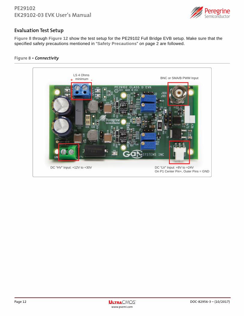
Evaluation Test SetupFigure 8 through Figure 12 show the test setup for the PE29102 Full Bridge EVB setup. Make sure that the specified safety precautions mentioned in “Safety Precautions” on page 2 are followed.
Figure 8 • Connectivity
BNC or SMA/B PWM InputLS 4 Ohms minimum
DC “LV” Input: +8V to +24VOn P1 Center Pin+, Outer Pins = GND
DC “HV” Input: +12V to +30V
+ -
Page 12 DOC-82956-3 – (10/2017)www.psemi.com

PE29102EK29102-03 EVK User’s Manual
Figure 9 • "XOR" Derived Phase Inversion Jumper Settings
Figure 10 • Jumper Settings for PE29102 Derived Phase Inversion
“XOR” Phase Inversion Jumper Settings
Jumper Positions for Internal PE29102 Phase Inversion
DOC-82956-3 – (10/2017) Page 13www.psemi.com

PE29102EK29102-03 EVK User’s Manual
Figure 11 • Adjustments and Indicator
RDHL
Dead-time Adjustments - One Side
OCPLED
Dead-time Adjustments - Other SideOvercurrent Protection SensitivityFully Clockwise = ~3A, Fully CCW = ~12A
RDLH
RDHL
RDLH
Figure 12 • Test Points
Switch Node Oscilloscope GND
PWM Direct I/Ps to PE29102s+ Audio Out Audio Out -
Switch Nodes Load to Ground for CurrentMonitor Threshold Set and Test
Page 14 DOC-82956-3 – (10/2017)www.psemi.com

PE29102EK29102-03 EVK User’s Manual
Hardware OperationThe general guidelines for operating the evaluation board are listed in this section. Follow the steps to configure the hardware properly for operation.
1) Before proceeding, set the current limits to 0.5 A for the nominal +12V DC VDD supply feeding P1 (to begin,
start with 1A for the HV supply VIN feeding J7 at your chosen voltage of between +12 and +30V DC). Then
verify that all DC power supplies are turned off.
2) Verify that the dead time resistors R51, R52, R53 and R54 are all set to approximately 75 kΩ. Turning R68 fully clockwise establishes an overcurrent limit of approximately 3A on the PCB. At a later time, this setting can be advanced fully counter-clockwise to set a maximum on-board limit of approximately 12A, while mid-way/center (as shipped) should correspond to approximately 8A.
3) Connect the VDD power supply to P1, +ve is to the center pin, with the outer two pins being GND/0V.
4) Apply between +8 and +24V DC to P1 to power the PE29102 driver. With no load or HV supply yet connected, the current consumption should be ~20 mA.
5) Connect the input PWM control signal to J100. In the absence of a periodic rectangular waveform (which when present should be no greater than 80% duty cycle), device overheating may occur when in a permanent “high” quiescent state when a load is connected.
6) Set the function generator output impedance to 50Ω and supply a pulse output of 5VPP at 2.5V offset. Start
with a 50% duty cycle at a frequency between 200 and 400 kHz. Increase in the current consumption at P1 to ~25mA. With a dual-trace oscilloscope, use two probes to check that two anti-phase square waveforms are present on TP1 and TP2 as long as the jumper settings on J200 and J3 are set for this.
7) Connect the input power supply bus VIN (+) and (-) to J7. Use the 1A current limit on the supply until correct
operation is established. This, and the Overcurrent protection threshold trimmer R68, may be increased/rotated counter-clockwise accordingly.
8) Turn on the bus voltage to the required value. Do not exceed the absolute maximum voltage of +30V DC.
9) Connect a loudspeaker or resistive load to J8.
10)Once operational, adjust the bus voltage and PWM control within the operating range and observe the output switching behavior at test points JP2 and JP3. Exercise care not to short these nodes to their adjacent ground pins.
11)Apply the modulating PWM input signal. As switching frequency and output load increase, exercise care not to exceed the junction temperature of the devices.
12)To power down the evaluation board, follow the above steps in reverse.
Note: When measuring the high frequency content switch node, care must be taken to avoid long ground leads. Measure the switch node by placing the oscilloscope probe tip at JP2 and JP3 (designed for this purpose). See Figure 13 for proper probe technique.
PWM signal definition: A 5V amplitude, TTL compatible (i.e., 2.5V offset) rectangular pulse wave with a nominally 50% duty cycle, whose pulse width may be increased to 80% (or 5:1 Mark:Space ratio) to achieve maximum modulation depth for Class D pulse width modulated switching of the Full Bridge. A 50:50 square wave will produce the smallest output because each half of the bridge is modulated by an equal and opposite amount.
DOC-82956-3 – (10/2017) Page 15www.psemi.com

PE29102EK29102-03 EVK User’s Manual
Current Limit Calibration and Test ProcedureAll units are pre-calibrated and tested to a maximum current limit of 10 Amperes. To alter that, use the following procedure.
1) Using Ohms law, calculate and choose a representative maximum chosen resistive or active load (repre-senting no more than 14 Amps). This connection should be made between TP5 and ground, using sufficiently thick, short wires.
2) Disconnect all signal inputs and outputs. Connect the low voltage (~12V DC) supply to P1, taking care of the polarity.
3) Limit the current here to ~0.1A in case of accidental polarity reversal, and then apply the chosen High Voltage (up to 30V DC) to J7.
4) Once correct polarity is established, raise the current limit until the full supply voltage at J7 is reached.
5) Adjust R68 until the LED DS-1 just extinguishes. The current limit now matches what you are loading TP5 with to ground.
6) Power down and disconnect load. The board is now ready for use.
Figure 13 • Proper Oscilloscope Probe Measurement Technique
Do not use probe ground lead
Use ground clip attached to probe
ground sleeve
Place probe tip on probe pad
Minimize loop
Probe pads close to device under test
Page 16 DOC-82956-3 – (10/2017)www.psemi.com
PE29102EK29102-03 EVK User’s Manual
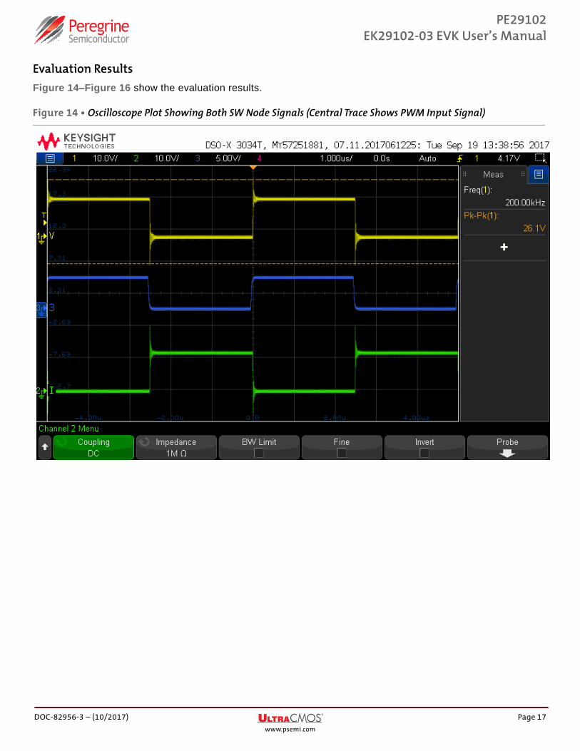
Evaluation Results Figure 14–Figure 16 show the evaluation results.
Figure 14 • Oscilloscope Plot Showing Both SW Node Signals (Central Trace Shows PWM Input Signal)
DOC-82956-3 – (10/2017) Page 17www.psemi.com

PE29102EK29102-03 EVK User’s Manual
Figure 15 • Audio 1 kHz Sine Wave Signal Recovered at Loudspeaker Output from a 200 kHz PWM Input Signal (Shown in the Background)
Page 18 DOC-82956-3 – (10/2017)www.psemi.com

PE29102EK29102-03 EVK User’s Manual
Figure 16 • PE29102 EVB Efficiency (%) Plotted Against Output Current (in A) with a 30V DC Supply and Output into an 8 Ohm Resistive Load, by Varying the Mark:Space Ratio of a 384 kHz PWM Signal
0
10
20
30
40
50
60
70
80
90
100
0 0.2 0.4 0.6 0.8 1 1.2 1.4 1.6 1.8 2
Effic
ienc
y (%
)
Output Current (A)
DOC-82956-3 – (10/2017) Page 19www.psemi.com

PE29102EK29102-03 EVK User’s Manual
Thermal ConsiderationsThe evaluation board includes four GS61004B transistors. Although the electrical performance surpasses that for traditional silicon devices, their relatively smaller size does magnify the thermal management requirements. The evaluation board is intended for bench evaluation with low ambient temperature and convection cooling. The addition of heat-sinking and forced air cooling can significantly increase the current rating of these devices, but care must be taken to not exceed the absolute maximum die temperature of +125 °C.
The thermal performance of the PE29102/GS61004B evaluation board is shown in Figure 17.
With a 5:1 duty cycle corresponding to a near-maximum pulse width modulation index into a suitable load, the hottest components are the resistors in the Zobel/Snubber Networks (if/when fitted) and the inductors. However, in the absence of a periodic PWM input, the steady DC quiescent state will draw a significantly higher standing current through the GaN FETs; consequently, care and heatsinking considerations will be required to accommodate the resulting increased temperatures.
Note: The switch node snubber networks were fitted at the time the thermal images were taken: that is, R39 and C27, R27 and C19, whose resistors will become hot if fitted, as seen in these images. Leaving these parts unfitted should improve efficiency slightly.
Figure 17 • PE29102/GS61004B EVB Thermal Plot Showing Maximum of 57C with PWM 1.26 S Pulse Width at 200 kHz, with 30V @1 A on HV PSU into 8 Ohm Resistive Load
Page 20 DOC-82956-3 – (10/2017)www.psemi.com

PE29102EK29102-03 EVK User’s Manual
Guidelines for Half-Bridge Stereo Audio OperationThis Full Bridge design can be operated as two independent half-bridges by performing the following simple modifications:
1) Remove C20, C21 and R29.
2) Fit a pair of 63V or greater 0.22 F film capacitors to positions C32 and C33. These are essential to form the output low pass filters with L2 and L1, respectively in the absence of C20.
3) Remove any jumper links from J200 and J3, as these would otherwise drive the two half bridges simultane-ously, whether in or out of phase. Unless that is still desirable, these jumpers will need to be removed and the incoming PWM signals instead applied directly to TP1 and TP2, for example as a Stereo pair of Left and Right channels. D1 and D2 still protect the PE29102 inputs that are connected. Do not use the coax socket at J100/101, as U9 and U5 are now redundant. Pull down resistors to ground may be required from TP1 and TP2 and if so, these should be 10k.
4) To avoid using the common output J8, use TP3 and TP4 for one channel and TP6 and TP7 for the other, which will be less confusing.
Note: For an adequate low frequency response, a large electrolytic capacitor (of at least 63V working voltage and a value of at least 2200 F or higher MUST be fitted in series with both TP3 and TP6 or socket J8: each positive capacitor terminal should go to these, respectively. Failing to observe this required DC blocking will result in damage to your loudspeakers.
The loudspeakers must be connected after the DC blocking electrolytic capacitors, then to ground: that is, there must be no DC voltage present across the loudspeaker voice coils.
The negative capacitor terminals should go to the + speaker connections, with the – speaker connections both going to Ground, preferably starred from Pin 1 J7, the DC power inlet ground terminal.
DOC-82956-3 – (10/2017) Page 21www.psemi.com

PE29102EK29102-03 EVK User’s Manual
Figure 18 • Half-Bridge Stereo Audio Operation Configuration
A 2200uF @ 63V Capacitor MUST be fitted in series with each LS (Loudspeaker): Connect the positive (+) end of LS to each positive (+) PCB output connection. Connect the negative (-) end of capacitor to the LS positive terminal.
Note: * Negative LS terminals connect to GND (see Figure 19).
• Connect the positive (+) end of each external 2200 F 63V electrolytic capacitor to each positive (+) PCB output connection. • Connect the negative (-) end of each of these capacitors to the respective LS positive terminals.• Negative LS terminals connect to GND (see block diagram).
Fit these two 0.22 µF @ 63V Capacitors
Fit these two jumpersCh1+*
Ch1PWM in
Ch2PWM in
Ch2+*
GNDGND
L.S. Outputs:
Remove these three components Do NOT fit jumpers here
Do NOT use this socket
Page 22 DOC-82956-3 – (10/2017)www.psemi.com

PE29102EK29102-03 EVK User’s Manual
Figure 19 • Modified Block Diagram for Independent Dual (Stereo) Half-Bridge Topology
PE29102Gate Driver
#1
PE29102Gate Driver
#2
VIN VIN
L TP6 TP31 L2
CF(C33)
RPMWI/P
(TP2)
LPMWI/P
(TP1)
CF(C32)
R(L.S.)
CL
+
+
-
GNDCF = Low-pass audio filter capacitors
CL = Large D.C. Blocking / A.C.Coupling Capacitors
Not Used(Jumper links removed from J200, J3
VSW1 VSW2
LogicBuffer
LogicPhaseSplitter
L(L.S.)
CL
+
+
-
GateDrive
Regulator
DOC-82956-3 – (10/2017) Page 23www.psemi.com

PE29102EK29102-03 EVK User’s Manual
This page intentionally left blank.
Page 24 DOC-82956-3 – (10/2017)www.psemi.com

4
PE29102EK29102-03 EVK User’s Manual
Technical Resources
Technical Resources Additional technical resources are available for download in the Products section at www.psemi.com. These include the Product Specification datasheet, S-parameters, zip file, evaluation kit schematic and bill of materials, material declaration form and PC-compatible software file.
Trademarks are subject to trademark claims.
DOC-82956-3 – (102017) Page 25www.psemi.com

PE29102EK29102-03 EVK User’s Manual
This page intentionally left blank.
Page 26 DOC-82956-3 – (102017)www.psemi.com