Impact of Stencil Foil Type on Solder Paste Transfer...
8
Originally published in the Proceedings of SMTA International, Rosemont, IL, Sept. 17 – 21, 2017 Impact of Stencil Foil Type on Solder Paste Transfer Efficiency for Laser Cut SMT Stencils Greg Smith BlueRing Stencils Lumberton, NJ, USA [email protected] ABSTRACT There are many different metal foil types being used by stencil manufacturers in today’s SMT market. Some of these materials include standard 300 series stainless foil, fine grain foil, electroplated nickel foil along with other specialty foils optimized for the laser cut stencil industry. This paper will investigate laser cut wall quality on the different foils as well as the effectiveness of these foil types in relation to solder paste printing both with and without nano-coatings. Results will be presented along with strengths and weaknesses of different foil types to aid the end user in making proper stencil choices. Keywords: SMT stencil, stencil printing, laser cut stencil, stencil foil material, SMT stencil quality, solder paste printing INTRODUCTION As innovation and demand continue to drive miniaturization in electronics, manufacturers face the constant challenge of assembling smaller and smaller components with repeatable processes and high yields. Stencil printing is the first step in the PWB assembly process and improvements to the SMT stencil can significantly improve yields, especially for more challenging miniaturized products [1]. The primary inputs in the SMT stencil manufacturing process are material, equipment and processes and by continuously improving these inputs the overall print process is improved. The most important material in the process of manufacturing SMT stencils is the foil itself. This paper investigates foil types used with the goal of determining which foils provide the best print performance. The two foil alloys examined are stainless steel and electroformed nickel sheet and each material will be measured with and without the application of ceramic nano-coatings. There have been many claims by stencil manufacturers in the industry over the past several years that fine grain foils cut and release solder paste better than other more standard stainless steel foils. However, the term “Fine Grain” has been used loosely and has not been well defined. Some users see print improvements using fine grain materials and some do not. This paper correlates print performance to grain size of each material tested and seeks to determine if foil grain size is a primary factor in obtaining optimal print performance. The term “print performance” is characterized by assessing transfer efficiency as well as print variation across a range of area ratios on both uncoated and ceramic, nano-coated stencils for each material. SEM photographs are also presented showing the surface topography of the sidewalls of the apertures after laser cutting. The SEM results are compared to the paste transfer efficiencies of each material to better understand how aperture wall surface smoothness compares to SMT stencil performance. This study will show that the base foil used to manufacture SMT stencils does in fact play an important role in overall stencil performance and is one of the most important inputs to provide the most consistent print process. EXPERIMENTAL METHODOLOGY A test vehicle was created that would show transfer efficiency over a wide array of area ratios. All seven materials are five- mils thick (125 microns) and a rounded square was used to design each aperture. Each area ratio includes 100 apertures. The test vehicle is shown below (Figure 1). Figure 1: Test Vehicle. Two test vehicle patterns were laser cut into each stencil. One pattern on each stencil was coated with a ceramic nano- coating and the other pattern was not coated. Two coupons were also cut into the top left and top right corners of each stencil. The coupons were outlined with a perforated pattern so they could be removed and sent for SEM processing. The overall stencil image and coupon is shown below (Figure 2).
-
Upload
hoangkhuong -
Category
Documents
-
view
217 -
download
4
Transcript of Impact of Stencil Foil Type on Solder Paste Transfer...
Originally published in the Proceedings of SMTA International, Rosemont, IL, Sept. 17 – 21, 2017
Impact of Stencil Foil Type on Solder Paste Transfer Efficiency for
Laser Cut SMT Stencils
Greg Smith
BlueRing Stencils
Lumberton, NJ, USA
ABSTRACT
There are many different metal foil types being used by
stencil manufacturers in today’s SMT market. Some of
these materials include standard 300 series stainless foil,
fine grain foil, electroplated nickel foil along with other
specialty foils optimized for the laser cut stencil industry.
This paper will investigate laser cut wall quality on the
different foils as well as the effectiveness of these foil types
in relation to solder paste printing both with and without
nano-coatings. Results will be presented along with
strengths and weaknesses of different foil types to aid the
end user in making proper stencil choices.
Keywords: SMT stencil, stencil printing, laser cut stencil,
stencil foil material, SMT stencil quality, solder paste
printing
INTRODUCTION
As innovation and demand continue to drive miniaturization
in electronics, manufacturers face the constant challenge of
assembling smaller and smaller components with repeatable
processes and high yields. Stencil printing is the first step in
the PWB assembly process and improvements to the SMT
stencil can significantly improve yields, especially for more
challenging miniaturized products [1]. The primary inputs in
the SMT stencil manufacturing process are material,
equipment and processes and by continuously improving
these inputs the overall print process is improved.
The most important material in the process of manufacturing
SMT stencils is the foil itself. This paper investigates foil
types used with the goal of determining which foils provide
the best print performance. The two foil alloys examined are
stainless steel and electroformed nickel sheet and each
material will be measured with and without the application of
ceramic nano-coatings. There have been many claims by
stencil manufacturers in the industry over the past several
years that fine grain foils cut and release solder paste better
than other more standard stainless steel foils. However, the
term “Fine Grain” has been used loosely and has not been
well defined. Some users see print improvements using fine
grain materials and some do not. This paper correlates print
performance to grain size of each material tested and seeks to
determine if foil grain size is a primary factor in obtaining
optimal print performance.
The term “print performance” is characterized by assessing
transfer efficiency as well as print variation across a range of
area ratios on both uncoated and ceramic, nano-coated
stencils for each material. SEM photographs are also
presented showing the surface topography of the sidewalls of
the apertures after laser cutting. The SEM results are
compared to the paste transfer efficiencies of each material to
better understand how aperture wall surface smoothness
compares to SMT stencil performance. This study will show
that the base foil used to manufacture SMT stencils does in
fact play an important role in overall stencil performance and
is one of the most important inputs to provide the most
consistent print process.
EXPERIMENTAL METHODOLOGY
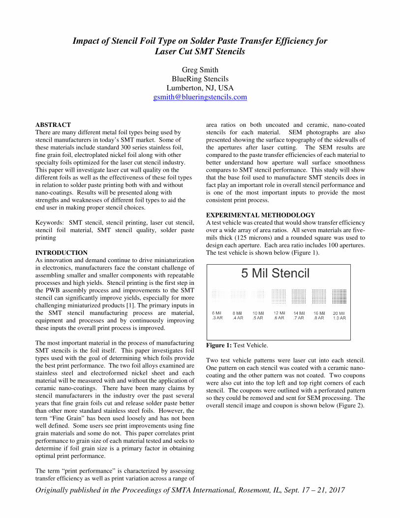
A test vehicle was created that would show transfer efficiency
over a wide array of area ratios. All seven materials are five-
mils thick (125 microns) and a rounded square was used to
design each aperture. Each area ratio includes 100 apertures.
The test vehicle is shown below (Figure 1).
Figure 1: Test Vehicle.
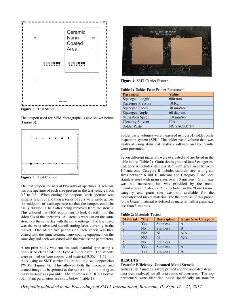
Two test vehicle patterns were laser cut into each stencil.
One pattern on each stencil was coated with a ceramic nano-
coating and the other pattern was not coated. Two coupons
were also cut into the top left and top right corners of each
stencil. The coupons were outlined with a perforated pattern
so they could be removed and sent for SEM processing. The
overall stencil image and coupon is shown below (Figure 2).
Originally published in the Proceedings of SMTA International, Rosemont, IL, Sept. 17 – 21, 2017
Figure 2. Test Stencil.
The coupon used for SEM photographs is also shown below
(Figure 3).
Figure 3: Test Coupon.
The test coupon consists of two rows of apertures. Each row
has one aperture of each size present in the test vehicle from
0.3 to 0.8. When cutting the coupons, each aperture was
initially laser cut and then a series of cuts were made across
the midpoint of each aperture so that the coupon could be
easily divided in half after being removed from the stencil.
This allowed the SEM equipment to look directly into the
sidewalls of the apertures. All stencils were cut on the same
stencil on the same day with the same settings. The laser used
was the most advanced stencil cutting laser currently in the
market. One of the two patterns on each stencil was then
coated with the same ceramic nano-coating equipment on the
same day and each was cured with the exact same parameters.
A ten-print study was run for each material type using a
popular no clean SAC305, Type 4 solder paste. The stencils
were printed on bare copper clad material 0.062” (1.57mm)
thick using an SMT carrier fixture holding two copper clad
PWB’s (Figure 4). This allowed both the uncoated and
coated image to be printed at the same time minimizing as
many variables as possible. The printer was a DEK Horizon
02i. Print parameters are show below (Table 1).
Figure 4: SMT Carrier Fixture.
Table 1: Solder Paste Printer Parameters.
Parameter Value
Squeegee Length 600 mm
Squeegee Pressure 10 Kg
Squeegee Speed 30 mm/sec
Squeegee Angle 60 degrees
Separation Speed 1.0 mm/sec
Cleaning Solvent IPA
Solder Paste NC SAC305 T4
Solder paste volumes were measured using a 3D solder paste
inspection system (SPI). The solder paste volume data was
analyzed using statistical analysis software and the results
were presented.
Seven different materials were evaluated and are listed in the
table below (Table 2). Grain size is grouped into 3 categories.
Category A includes stainless steel with grain sizes between
1-5 microns. Category B includes stainless steel with grain
sizes between 6 and 10 microns and Category C includes
stainless steel with grain sizes over 10 microns. Grain size
was not measured but was provided by the metal
manufacturer. Category A is included in the “Fine Grain”
category and grain size was not available for the
electroformed nickel material. For the purpose of this paper,
“Fine Grain” material is defined as material with a grain size
less than 5 microns.
Table 2: Materials Tested.
Material “FG” Description Grain Size Category
1 Yes Stainless A
2 No Stainless B
3 N/A Ni N/A
4 N/A Ni N/A
5 No Stainless C
6 Yes Stainless A
7 Yes Stainless A
RESULTS
Transfer Efficiency -Uncoated Metal Stencils
Initially, all 7 materials were printed and the uncoated stencil
data was analyzed for all area ratios of apertures. The top
performers were identified based specifically on transfer
Originally published in the Proceedings of SMTA International, Rosemont, IL, Sept. 17 – 21, 2017
efficiency in this analysis. The results are seen below (Figure
5) and show that materials 1 and 2 exhibit better print transfer
efficiencies with uncoated apertures than the other materials.
Figure 5: Transfer Efficiency of Uncoated Stencils: All area
ratios and metal types.
Since small area ratio printing is key in product
miniaturization, it is important to determine which uncoated
material performed the best from 0.3 thru 0.5 area ratios.
These area ratios are defined as small area ratio printing
because they are below the recommendation in IPC7525B
standard of 0.66 [2]. The following figure (Figure 6) shows
the results for 0.3, 0.4 and 0.5 area ratio apertures only.
Figure 6: Transfer Efficiency of Uncoated Stencils: All
metals, 0.3, 0.4 and 0.5 area ratios.
As shown above, metal 1 has the highest transfer efficiency
results versus the other metals for the 0.3, 0.4 and 0.5 area
ratio prints. It also outperformed the second-best material,
material2, when comparing the means by over 15%. Material
2 shows a 5% improvement over the third best material when
comparing mean transfer efficiencies (Table 3).
Table 3: Mean Transfer Efficiency of Uncoated Stencils for
0.3, 0.4 and 0.5 Area Ratios for all metal types.
Material
0.30
Area Ratio
0.40
Area Ratio
0.50
Area Ratio
1 28.04 38.31 96.85
2 10.45 27.71 89.6
3 5.94 23.35 82.46
4 5.31 25.49 93.95
5 8.49 24.44 82.52
6 6.45 24.12 81.32
7 6.05 22.14 84.63
Another interesting observation is that at 0.5 area ratio, the
differences in transfer efficiency results increase significantly
vs the 0.3 and 0.4 area ratios with materials 1, 2 and 4 easily
surpassing the 80% transfer efficiency numbers typically
required to pass SPI. Using Tukey-Kramer HSD, material 1
is statistically the best performing material when measuring
transfer efficiency on small area ratio apertures (Figure 7) and
material 2 are statistically in the second best performing
group for transfer efficiency with the highest mean transfer
efficiency in that group.
Figure 7: Tukey-Kramer HSD on Transfer Efficiency for
Area Ratio 0.3, 0.4 and 0.5.
The final analysis on uncoated stencil foils is to examine
larger area ratios to understand if material type affects
transfer efficiency. All materials where observed printing at
area ratios 0.6, 0.7 and 0.8. The following chart shows the
results (Figure 8).
Figure 8: Transfer Efficiency of Uncoated Stencils: All
metals, 0.6, 0.7, and 0.8 area ratios.
Originally published in the Proceedings of SMTA International, Rosemont, IL, Sept. 17 – 21, 2017
Once again, it can be observed that metal 1 and 2 outperform
the others when measuring transfer efficiency for the larger
area ratios. Mean transfer efficiency for metal 1 was greater
than the mean of metal 2 by just under 5% and the mean
transfer efficiency for metal 2 was 5% better than the next
best performing metal 4. Again, we see a large increase in
transfer efficiency when moving from 0.6 and 0.7 area ratio
printing to 0.8 area ratio printing.
Transfer Efficiency-Ceramic Nano-Coated Metal Stencils
Ceramic nano-coated metal stencils are becoming more
widely used in today’s assembly environment to achieve the
best print possible, especially for low area ratio printing. It
has been shown in previously published papers these coatings
improve transfer efficiency by 10% up to 24% [3] based on
the size of the aperture and the brand and particle size of
solder paste being used. To properly evaluate the different
metal materials being used to manufacture SMT stencils, it is
important to include the ceramic nano-coating technology in
this study. The objective is to evaluate if specific material
types improve the effect of the coating technology.
Initially, all seven metal foils were analyzed for all area
ratios. Again, the top performers were identified based
specifically on transfer efficiency. The image below shows
the results of both uncoated and coated stencil materials for
all area ratios combined (Figure 9).
Figure 9: Transfer Efficiency for Coated and Uncoated
Stencils for All Metals and All Area Ratios.
The top performers for ceramic nano-coated stencils for all
area ratios measured are materials 1 and 2. When measuring
the mean transfer efficiency of the coated stencil vs uncoated
stencil, material 1 improves transfer efficiency by 8.2%.
Material 2 shows an improvement with coating of 6.5% vs
the uncoated material. Comparing coated stencil transfer
efficiency, material 1 improves transfer efficiency 10.2%
more than material 2. Material 2 improves transfer efficiency
more than material 4, the third best performer, by just under
4%. One can also see that the improvement in transfer
efficiency created by the ceramic nano-coating technology
closely follows the release characteristics of the base metal
being cut. This phenomenon shows the importance of
selecting the best possible base material in the stencil
manufacturing environment.
To further evaluate the ceramic, nano-coating technology it
is critical to look at small area ratio printing defined in this
paper as apertures with area ratios of 0.3, 0.4 and 0.5. The
image below (Figure 10) shows the improved release
characteristics with the addition of the ceramic nano-coating.
Figure 10: Transfer Efficiency for Coated and Uncoated
Stencils for All Metals with 0.3, 0.4, and 0.5 Area Ratios
combined.
The coated material exhibiting the best mean transfer
efficiency for area ratios of 0.3, 0.4 and 0.5 combined is
material 1. When averaging these three area ratios, an
increase in mean transfer efficiency with the ceramic nano-
coating is 16% versus the uncoated stencil. Material 2 with
the coating technology had the second highest mean transfer
efficiency improvement of just under 16% as well. Overall,
a larger improvement in transfer efficiency is seen on small
area ratios with the application of the ceramic nano-coating
technology versus the larger area apertures. Again, it should
be noted that the improvement in solder paste release from
the nano-coated stencil follows the transfer efficiency of the
base material especially on small area ratio apertures.
Currently most stencil providers limit lower area ratios to 0.6
to maintain proper release and volume to achieve acceptable
solder fillets after reflow. Observing the data in the chart
below (Figure 11) one can see that material 3, 5, 6 and 7 are
close to 80% transfer efficiency on 0.5 area ratio apertures
with no coating (blue bars) and materials 1, 2 and 4 are just
at or over 90% with no coating (blue bars). When the ceramic
nano-coating is added, the transfer efficiency mean for
material 1 increases 28% to 125% (orange bars). With the
best base material and the ceramic coating technology, small
aperture printing at 0.5 area ratios is now possible.
Originally published in the Proceedings of SMTA International, Rosemont, IL, Sept. 17 – 21, 2017
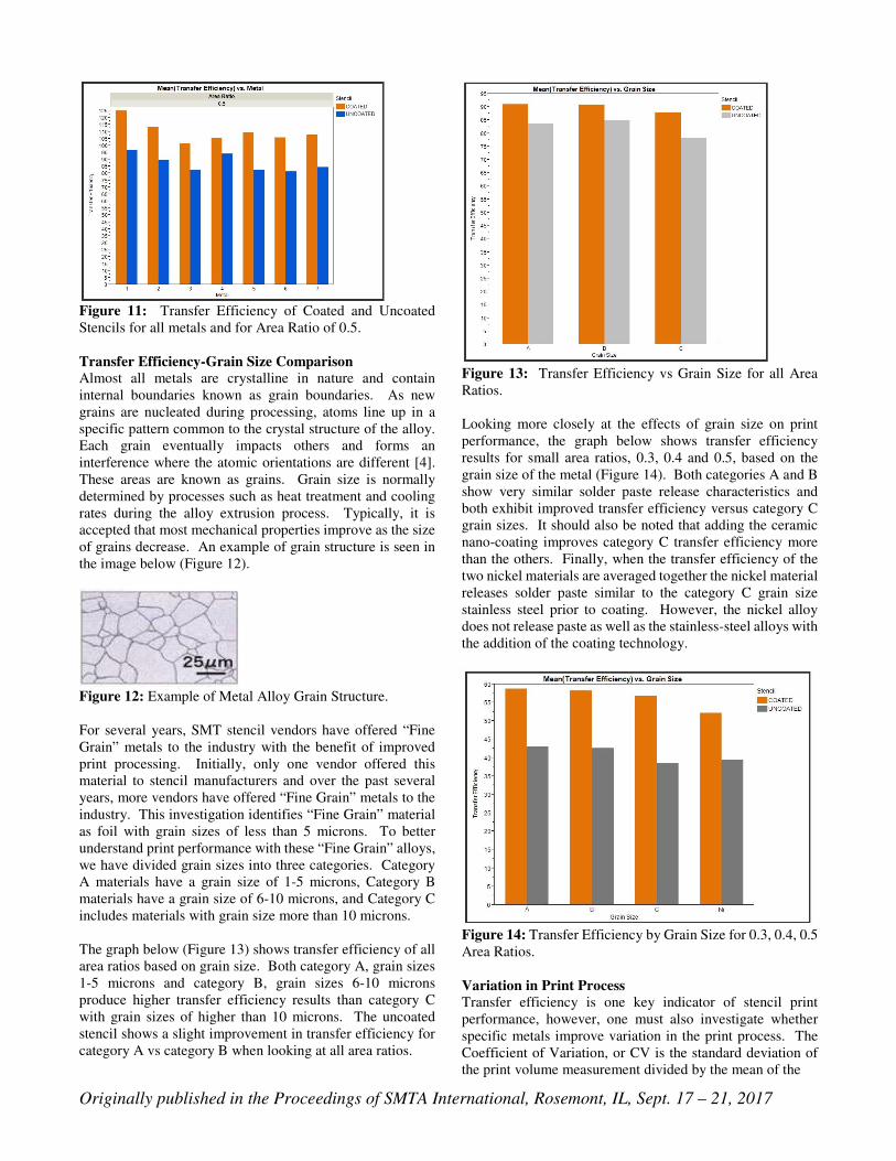
Figure 11: Transfer Efficiency of Coated and Uncoated
Stencils for all metals and for Area Ratio of 0.5.
Transfer Efficiency-Grain Size Comparison
Almost all metals are crystalline in nature and contain
internal boundaries known as grain boundaries. As new
grains are nucleated during processing, atoms line up in a
specific pattern common to the crystal structure of the alloy.
Each grain eventually impacts others and forms an
interference where the atomic orientations are different [4].
These areas are known as grains. Grain size is normally
determined by processes such as heat treatment and cooling
rates during the alloy extrusion process. Typically, it is
accepted that most mechanical properties improve as the size
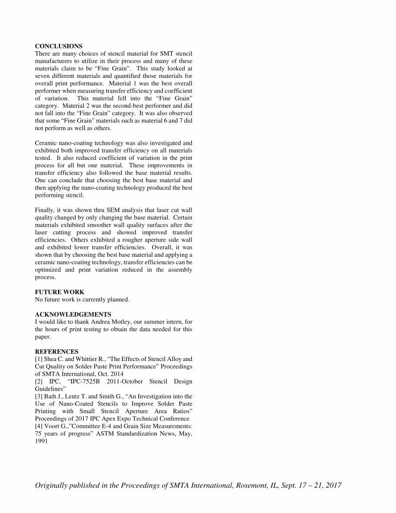
of grains decrease. An example of grain structure is seen in
the image below (Figure 12).
Figure 12: Example of Metal Alloy Grain Structure.
For several years, SMT stencil vendors have offered “Fine
Grain” metals to the industry with the benefit of improved
print processing. Initially, only one vendor offered this
material to stencil manufacturers and over the past several
years, more vendors have offered “Fine Grain” metals to the
industry. This investigation identifies “Fine Grain” material
as foil with grain sizes of less than 5 microns. To better
understand print performance with these “Fine Grain” alloys,
we have divided grain sizes into three categories. Category
A materials have a grain size of 1-5 microns, Category B
materials have a grain size of 6-10 microns, and Category C
includes materials with grain size more than 10 microns.
The graph below (Figure 13) shows transfer efficiency of all
area ratios based on grain size. Both category A, grain sizes
1-5 microns and category B, grain sizes 6-10 microns
produce higher transfer efficiency results than category C
with grain sizes of higher than 10 microns. The uncoated
stencil shows a slight improvement in transfer efficiency for
category A vs category B when looking at all area ratios.
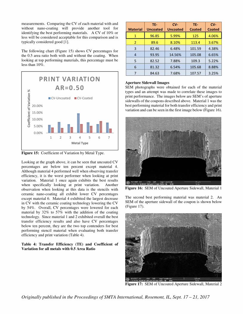
Figure 13: Transfer Efficiency vs Grain Size for all Area
Ratios.
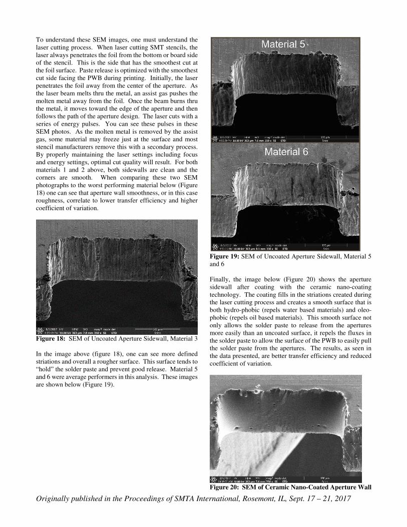
Looking more closely at the effects of grain size on print
performance, the graph below shows transfer efficiency
results for small area ratios, 0.3, 0.4 and 0.5, based on the
grain size of the metal (Figure 14). Both categories A and B
show very similar solder paste release characteristics and
both exhibit improved transfer efficiency versus category C
grain sizes. It should also be noted that adding the ceramic
nano-coating improves category C transfer efficiency more
than the others. Finally, when the transfer efficiency of the
two nickel materials are averaged together the nickel material
releases solder paste similar to the category C grain size
stainless steel prior to coating. However, the nickel alloy
does not release paste as well as the stainless-steel alloys with
the addition of the coating technology.
Figure 14: Transfer Efficiency by Grain Size for 0.3, 0.4, 0.5
Area Ratios.
Variation in Print Process
Transfer efficiency is one key indicator of stencil print
performance, however, one must also investigate whether
specific metals improve variation in the print process. The
Coefficient of Variation, or CV is the standard deviation of
the print volume measurement divided by the mean of the
Originally published in the Proceedings of SMTA International, Rosemont, IL, Sept. 17 – 21, 2017
measurements. Comparing the CV of each material with and
without nano-coating will provide another tool for
identifying the best performing materials. A CV of 10% or
less will be considered acceptable for this comparison and is
typically considered good [1].
The following chart (Figure 15) shows CV percentages for
the 0.5 area ratio both with and without the coating. When
looking at top performing materials, this percentage must be
less than 10%.
Figure 15: Coefficient of Variation by Metal Type.
Looking at the graph above, it can be seen that uncoated CV
percentages are below ten percent except material 4.
Although material 4 performed well when observing transfer
efficiency, it is the worst performer when looking at print
variation. Material 1 once again exhibits the best results
when specifically looking at print variation. Another
observation when looking at this data is the stencils with
ceramic nano-coating all exhibit lower CV percentages
except material 6. Material 4 exhibited the largest decrease
in CV with the ceramic coating technology lowering the CV
by 54%. Overall, CV percentages were lowered for each
material by 32% to 57% with the addition of the coating
technology. Since material 1 and 2 exhibited overall the best
transfer efficiency results and also have CV percentages
below ten percent, they are the two top contenders for best
performing stencil material when evaluating both transfer
efficiency and print variation (Table 4).
Table 4: Transfer Efficiency (TE) and Coefficient of
Variation for all metals with 0.5 Area Ratio
Aperture Sidewall Images
SEM photographs were obtained for each of the material
types and an attempt was made to correlate these images to
print performance. The images below are SEM’s of aperture
sidewalls of the coupons described above. Material 1 was the
best performing material for both transfer efficiency and print
variation and can be seen in the first image below (Figure 16).
Figure 16: SEM of Uncoated Aperture Sidewall, Material 1
The second best performing material was material 2. An
SEM of the aperture sidewall of the coupon is shown below
(Figure 17).
Figure 17: SEM of Uncoated Aperture Sidewall, Material 2
0.00%
5.00%
10.00%
15.00%
20.00%
1 2 3 4 5 6 7
Co
eff
icie
nt
of
Va
ria
tio
n %
Metal Type
PRINT VARIATION
AR=0.50
CV-Uncoated CV-Coated
Material
TE-
Uncoated
CV-
Uncoated
TE-
Coated
CV-
Coated
1 96.85 5.99% 125 4.06%
2 89.6 8.10% 113.4 3.67%
3 82.46 6.48% 101.59 4.38%
4 93.95 14.56% 105.08 6.65%
5 82.52 7.88% 109.3 5.22%
6 81.32 6.54% 105.68 8.88%
7 84.63 7.68% 107.57 3.25%
Originally published in the Proceedings of SMTA International, Rosemont, IL, Sept. 17 – 21, 2017
To understand these SEM images, one must understand the
laser cutting process. When laser cutting SMT stencils, the
laser always penetrates the foil from the bottom or board side
of the stencil. This is the side that has the smoothest cut at
the foil surface. Paste release is optimized with the smoothest
cut side facing the PWB during printing. Initially, the laser
penetrates the foil away from the center of the aperture. As
the laser beam melts thru the metal, an assist gas pushes the
molten metal away from the foil. Once the beam burns thru
the metal, it moves toward the edge of the aperture and then
follows the path of the aperture design. The laser cuts with a
series of energy pulses. You can see these pulses in these
SEM photos. As the molten metal is removed by the assist
gas, some material may freeze just at the surface and most
stencil manufacturers remove this with a secondary process.
By properly maintaining the laser settings including focus
and energy settings, optimal cut quality will result. For both
materials 1 and 2 above, both sidewalls are clean and the
corners are smooth. When comparing these two SEM
photographs to the worst performing material below (Figure
18) one can see that aperture wall smoothness, or in this case
roughness, correlate to lower transfer efficiency and higher
coefficient of variation.
Figure 18: SEM of Uncoated Aperture Sidewall, Material 3
In the image above (figure 18), one can see more defined
striations and overall a rougher surface. This surface tends to
“hold” the solder paste and prevent good release. Material 5
and 6 were average performers in this analysis. These images
are shown below (Figure 19).
Figure 19: SEM of Uncoated Aperture Sidewall, Material 5
and 6
Finally, the image below (Figure 20) shows the aperture
sidewall after coating with the ceramic nano-coating
technology. The coating fills in the striations created during
the laser cutting process and creates a smooth surface that is
both hydro-phobic (repels water based materials) and oleo-
phobic (repels oil based materials). This smooth surface not
only allows the solder paste to release from the apertures
more easily than an uncoated surface, it repels the fluxes in
the solder paste to allow the surface of the PWB to easily pull
the solder paste from the apertures. The results, as seen in
the data presented, are better transfer efficiency and reduced
coefficient of variation.
Figure 20: SEM of Ceramic Nano-Coated Aperture Wall
Originally published in the Proceedings of SMTA International, Rosemont, IL, Sept. 17 – 21, 2017
CONCLUSIONS
There are many choices of stencil material for SMT stencil
manufacturers to utilize in their process and many of these
materials claim to be “Fine Grain”. This study looked at
seven different materials and quantified those materials for
overall print performance. Material 1 was the best overall
performer when measuring transfer efficiency and coefficient
of variation. This material fell into the “Fine Grain”
category. Material 2 was the second-best performer and did
not fall into the “Fine Grain” category. It was also observed
that some “Fine Grain” materials such as material 6 and 7 did
not perform as well as others.
Ceramic nano-coating technology was also investigated and
exhibited both improved transfer efficiency on all materials
tested. It also reduced coefficient of variation in the print
process for all but one material. These improvements in
transfer efficiency also followed the base material results.
One can conclude that choosing the best base material and
then applying the nano-coating technology produced the best
performing stencil.
Finally, it was shown thru SEM analysis that laser cut wall
quality changed by only changing the base material. Certain
materials exhibited smoother wall quality surfaces after the
laser cutting process and showed improved transfer
efficiencies. Others exhibited a rougher aperture side wall
and exhibited lower transfer efficiencies. Overall, it was
shown that by choosing the best base material and applying a
ceramic nano-coating technology, transfer efficiencies can be
optimized and print variation reduced in the assembly
process.
FUTURE WORK
No future work is currently planned.
ACKNOWLEDGEMENTS I would like to thank Andrea Motley, our summer intern, for
the hours of print testing to obtain the data needed for this
paper.
REFERENCES [1] Shea C. and Whittier R., “The Effects of Stencil Alloy and
Cut Quality on Solder Paste Print Performance” Proceedings
of SMTA International, Oct. 2014
[2] IPC, “IPC-7525B 2011-October Stencil Design
Guidelines”
[3] Bath J., Lentz T. and Smith G., “An Investigation into the
Use of Nano-Coated Stencils to Improve Solder Paste
Printing with Small Stencil Aperture Area Ratios”
Proceedings of 2017 IPC Apex Expo Technical Conference
[4] Voort G.,”Committee E-4 and Grain Size Measurements:
75 years of progress” ASTM Standardization News, May,
1991