A Double-Tail Latch-Type Voltage Sense Amplifier With 18ps Setup+Hold Time

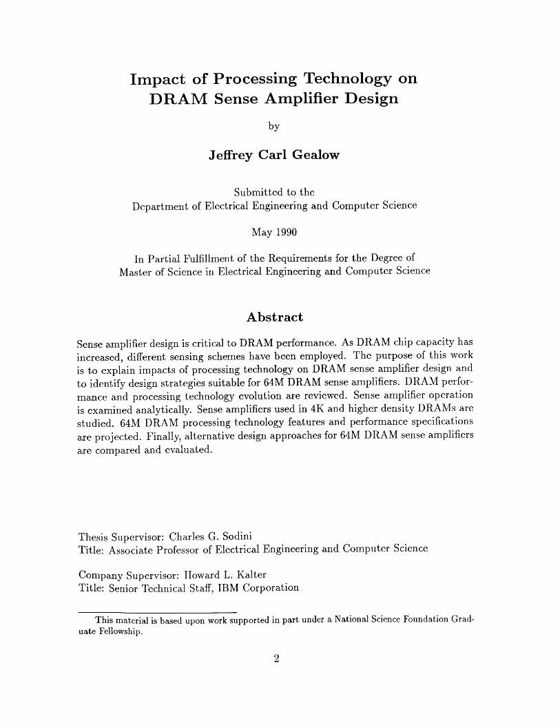
Impact of Processing Technology onDRAM Sense Amplifier Design
by
Jeffrey Carl Gealow
Submitted to the Department of Electrical Engineering and Computer Science
in Partial Fulfillment of the Requirements for the Degree of
Master of Science in Electrical Engineering and Computer Science
at the Massachusetts Institute of Technology
June 1990
@Jeffrey Carl Gealow, 1990. All rights reserved.
The author hereby grants to M.I.T permission to reproduce
and to distribute copies of this thesis document in whole or in part.
Signature of Author ___ _______________________Departm u oftflectrical Engineering and Computer Science
May 1990
Certified by
Associate Professor of Electrical Engineering andCharles G. SodiniComputer ScienceThesis Supervisor
Certified by
Accepted by
Howard L. Kalter
Senior Technical Staff, IBM Corporatione-visor
Arthur C. Smith
Chairman, Department Committee on Graduate Students
MASSACHUSETT S INSTITUTEOF TECHNOl OGY
AUG 10 1990
LIBRARIES
ARCH)VES
Impact of Processing Technology onDRAM Sense Amplifier Design
by
Jeffrey Carl Gealow
Submitted to the
Department of Electrical Engineering and Computer Science
May 1990
In Partial Fulfillment of the Requirements for the Degree of
Master of Science in Electrical Engineering and Computer Science
Abstract
Sense amplifier design is critical to DRAM performance. As DRAM chip capacity has
increased, different sensing schemes have been employed. The purpose of this work
is to explain impacts of processing technology on DRAM sense amplifier design and
to identify design strategies suitable for 64M DRAM sense amplifiers. DRAM perfor-
mance and processing technology evolution are reviewed. Sense amplifier operation
is examined analytically. Sense amplifiers used in 4K and higher density DRAMs are
studied. 64M DRAM processing technology features and performance specifications
are projected. Finally, alternative design approaches for 64M DRAM sense amplifiers
are compared and evaluated.
Thesis Supervisor: Charles G. SodiniTitle: Associate Professor of Electrical Engineering and Computer Science
Company Supervisor: Howard L. KalterTitle: Senior Technical Staff, IBM Corporation
This material is based upon work supported in part under a National Science Foundation Grad-uate Fellowship.

Acknowledgements
I have completed three MIT VI-A Internship Program assignments at the IBM
General Technology Division in Essex Junction, Vermont. This research was con-
ducted during my third assignment. I am grateful to past and present members
of Department A23 for their help. John Nickel served as my mentor during my
first assignment, patiently teaching me CMOS circuit design. Jim Yankosky, John
Barth, and John Nickel all provided invaluable computer assistance. Scott Lewis and
John Fifield contributed very useful sense amplifier design insights. Chuck Drake
graciously shared his computer with me. Outside of Department A23, Paul Smith
supplied DRAM trend information and provided graphics software guidance.I thank Howard Kalter, my manager and thesis supervisor at IBM, for making my
assignments both interesting and educational, for sharing his technical wisdom, and
for reviewing drafts of this thesis.I am grateful to Charles Sodini for supervising this thesis.
I thank my fiancde, Mary Condello, for helping me manage my bibliography, for
proofreading this thesis, for her support and encouragement, and for enduring several
long bus rides in order to visit me in Vermont.Finally, I thank my parents, Jon and Rita Gealow, for their love and support.

Sr-a--rn--m a

Contents
1 Introduction1.1 Divided Bitline Architecture . . . . . . . . . . . . . . .
1.1.1 Signal Loss Due to Incomplete Charge Transfer1.1.2 Dummy Storage Cells . . . . . . . . . . . . . . .
1.2 Noise Sources . . . . . . . . . . . . . . . . . . . . . . .1.3 Folded Bitline Architecture . . . . . . . . . . . . . . . .1.4 Balanced Flip-Flop Sense Amplifier . . . . . . . . . . .1.5 DRAM Evolution . . . . . . . . . . . . . . . . . . . . .
2 Theoretical Analysis of Sense Amplifier Operation2.1 Latching Pulse Optimization . . . . . . . .2.2 Sensitivity . . . . . . . . . . . . . . . . . .
2.2.1 Sense Amplifier Circuit Mismatches2.2.2 Published Sensitivity Analyses . . .2.2.3 Source-Coupled Pair Offset . . . . .2.2.4 Design Impacts . . . . . . . . . . .
3 Sense Amplifier Design Evolution3.1 4K DRAM Generation . . . . . . . . . . .
3.1.1 Texas Instruments . . . . . . . . .3.1.2 Microsystems International . . . . .
3.2 16K DRAM Generation . . . . . . . . . .3.2.1 Intel . . . . . . . . . . . . . . . . .3.2.2 Mostek . . . . . . . . . . . . . . . .
3.3 64K DRAM Generation . . . . . . . . . .3.3.1 IB M . . . . . . . . . . . . . . . . .3.3.2 Texas Instruments . . . . . . . . .3.3.3 Fairchild . . . . . . . . . . . . . . .
3.4 256K DRAM Generation . . . . . . . . . .3.4.1 Hitachi . . . . . . . . . . . . . . . .3.4.2 Intel . . . . . . . . . . . . . . . . .
3.5 IM DRAM Generation . . . . . . . . . . .3.5.1 Toshiba . . . . . . . . . . . . . . .3.5.2 Texas Instruments . . . . . . . . .
45. . . . . . . . . . . . . . . 45. . . . . . . . . . . . . . . 45. . . . . . . . . . . . . . . 48. . . . . . . . . . . . . . . 52. . . . . . . . . . . . . . . 52. . . . . . . . . . . . . . . 54. . . . . . . . . . . . . . . 57. . . . . . . . . . . . . . . 57. . . . . . . . . . . . . . . 59. . . . . . . . . . . . . . . 6 1. . . . . . . . . . . . . . . 64. . . . . . . - - - - - . . . 64. . . . . . . . . . . . . . . 65. . . . . . . . . . . . . . . 68. . . . . . . . . . . . . . . 68. . . . . . . . . . . . . . . 70
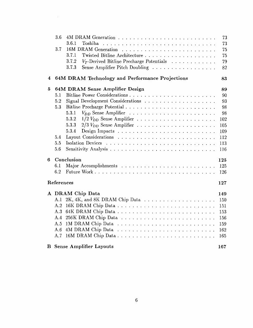
3.6 4M DRAM Generation ......................3.6.1 Toshiba ...........................
3.7 16M DRAM Generation ......................3.7.1 Twisted Bitline Architecture ...............3.7.2 VT-Derived Bitline Precharge Potentials . . . . .3.7.3 Sense Amplifier Pitch Doubling . . . . . . . . . .
4 64M DRAM Technology and Performance Projections
5 64M DRAM Sense Amplifier Design5.1 Bitline Power Considerations ...........5.2 Signal Development Considerations . . . . . . .5.3 Bitline Precharge Potential . . . . . . . . . . . .
5.3.1 VDD Sense Amplifier . . . . . . . . . . .5.3.2 1/2 VDD Sense Amplifier . . . . . . . . .5.3.3 2/3 VDD Sense Amplifier . . . . . . . . .5.3.4 Design Impacts . . . . . . . . . . . . . .
5.4 Layout Considerations . . . . . . . . . . . . . .5.5 Isolation Devices . . . . . . . . . . . . . . . . .5.6 Sensitivity Analysis . . . . . . . . . . . . . . . .
6 Conclusion6.1 Major Accomplishments . . . . . . . . . . . . .6.2 Future Work . . . . . . . . . . . . . . . . . . . .
89. . . . . . . . . . 90. . . . . . . . . . 93. . . . . . . . . . 98. . . . . . . . . . 98. . . . . . . . . . 102. . . . . . . . . . 105. . . . . . . . . . 109. . . . . . . . . . 112. . . . . . . . . . 113. . . . . . . . . . 116
125. . . . . . . . . . 125. . . . . . . . . . 126
References
A DRAM Chip DataA.1 2K, 4K, and 8K DRAM Chip Data . . . . . . . . . . . . . . . . . .A.2 16K DRAM Chip Data . . . . . . . . . . . . . . . . . . . . . . . . .A.3 64K DRAM Chip Data . . . . . . . . . . . . . . . . . . . . . . . . .A.4 256K DRAM Chip Data . . . . . . . . . . . . . . . . . . . . . . . .A.5 1M DRAM Chip Data . . . . . . . . . . . . . . . . . . . . . . . . .A.6 4M DRAM Chip Data . . . . . . . . . . . . . . . . . . . . . . . . .A.7 16M DRAM Chip Data . . . . . . . . . . . . . . . . . . . . . . . . .
B Sense Amplifier Layouts
737375757982
83
127
149150151153156159162165
167
List of Figures
1.1 DRAM Array .................................... 121.2 Divided Bit Line Architecture ...................... 141.3 Required Tolerance versus Number of Occurrences . . . . . . . . . . . 181.4 Folded Bit Line Architecture . . . . . . . . . . . . . . . . . . . . . . . 20
1.5 Stein et al. Balanced Flip-Flop Sense Amplifier . . . . . . . . . . . . 221.6 Access Time versus DRAM Generation . . . . . . . . . . . . . . . . . 241.7 Power per Bit versus DRAM Generation . . . . . . . . . . . . . . . . 24
1.8 Chip Area versus DRAM Generation . . . . . . . . . . . . . . . . . . 251.9 Cell Area versus DRAM Generation . . . . . . . . . . . . . . . . . . . 251.10 Feature Sizes versus DRAM Generation . . . . . . . . . . . . . . . . . 26
2.1 Cross-Coupled n-channel MOSFET Sense Amplifier Circuit . . . . . . 292.2 Optimal Latching Pulse Waveforms . . . . . . . . . . . . . . . . . . . 34
2.3 Source-Coupled MOSFET Pair . . . . . . . . . . . . . . . . . . . . . 41
3.1 TI 4K DRAM Sense Amplifier . . . . . . . . . . . . . . . . . . . . . . 463.2 Microsystems International 4K DRAM Sense Amplifier . . . . . . . . 49
3.3 Intel 16K DRAM Sense Amplifier . . . . . . . . . . . . . . . . . . . . 53
3.4 Mostek 16K DRAM Sense Amplifier . . . . . . . . . . . . . . . . . . 553.5 IBM 64K DRAM Sense Amplifier . . . . . . . . . . . . . . . . . . . . 583.6 TI 64K DRAM Sense Amplifier . . . . . . . . . . . . . . . . . . . . . 603.7 Fairchild 64K DRAM Sense Amplifier . . . . . . . . . . . . . . . . . . 623.8 Hitachi 256K DRAM Sense Amplifier . . . . . . . . . . . . . . . . . . 653.9 Intel 256K DRAM Sense Amplifier . . . . . . . . . . . . . . . . . . . 663.10 Toshiba IM DRAM Sense Amplifier . . . . . . . . . . . . . . . . . . . 693.11 TI 1M DRAM Sense Amplifier . . . . . . . . . . . . . . . . . . . . . . 713.12 Toshiba 4M DRAM Sense Amplifier . . . . . . . . . . . . . . . . . . . 74
3.13 Folded Bitline M odel . . . . . . . . . . . . . . . . . . . . . . . . . . . 763.14 Twisted Bitline Model . . . . . . . . . . . . . . . . . . . . . . . . . . 773.15 NTT 16M DRAM Sense Amplifier . . . . . . . . . . . . . . . . . . . . 803.16 2/3 VDD Sense Amplifier Circuit . . . . . . . . . . . . . . . . . . . . . 81
4.1 Bitline Coupling Capacitance . . . . . . . . . . . . . . . . . . . . . . 85
5.15.25.35.45.55.65.75.85.95.105.115.125.13
Uniform Array Patterns . . . . . . . . . . .Wordline Waveforms for Signal Developmentp-channel Array Signal Development . . . .n-channel Array Signal Development .
VDD Sense Amplifier Circuit . . . . . . . . .VDD Sense Amplifier Waveforms . . . . . . .VDD Sense Amplifier Device Currents . . . .1/2 VDD Sense Amplifier Circuit . . . . . . .1/2 VDD Sense Amplifier Waveforms . . . . .1/2 VDD Sense Amplifier Device Currents . .2/3 VDD Sense Amplifier Circuit . . . . . . .2/3 VDD Sense Amplifier Waveforms . . . . .2/3 VDD Sense Amplifier Device Currents . .
Analysis
5.14 Total Sense Amplifier Area versus Area per Sense Ampli5.15 Isolated n-channel Cross-Coupled Pair Waveforms . . .
. . . . . . . . 91
. . . . . . . . 95
. . . . . . . . 96
. . . . . . . . 97
. . . . . . . . 99
. . . . . . . . 100
. . . . . . . . 101. . . . . . . . 102. . . . . . . . 103. . . . . . . . 104. . . . . . . . 106. . . . . . . . 107. . . . . . . . 108fier ..... 112. . . . . . . . 118
5.16 VDD Sense Amplifier Signal After Sensing Operation v. Initial Signal 1195.17 VDD Sense Amplifier Average Off-Side Current v. Initial Signal . . . . 1205.18 VDD Sense Amplifier Offset due to Transistor Gain Mismatch . . . . . 1215.19 VDD Sense Amplifier Offset due to Bitline Capacitance Mismatch . . 1215.20 Non-Uniform Patterns for Process Variation Induced Offset Charac-
terization . . . . . . . . . . . . . . . . . . . . . . . . . . . . . . . . . . 1225.21 Patterns for Bitline Coupling Induced Offset Characterization . . . . 1235.22 VDD Sense Amplifier Offset due to Bitline-to-Bitline Coupling . . . . 124
B.1 Layout Legend . . . . . . . . . . . . . . . . . . . . . . . . . . . . . . 168B.2 VDD Sense Amplifier Layout . . . . . . . . . . . . . . . . . . . . . . . 169B.3 VDD Sense Amplifier n-channel Cross-Coupled Pair Layout . . . . . . 170B.4 VDD Sense Amplifier p-channel Cross-Coupled Pair Layout . . . . . . 171B.5 VDD Sense Amplifier Precharge and Equalization Device Layout . . . 172B.6 1/2 VDD Sense Amplifier Layout . . . . . . . . . . . . . . . . . . . . . 173B.7 1/2 VDD Sense Amplifier n-channel Cross-Coupled Pair Layout . . . . 174B.8 1/2 VDD Sense Amplifier p-channel Cross-Coupled Pair Layout . . . . 175B.9 1/2 VDD Sense Amplifier Precharge and Equalization Device Layout . 176B.10 2/3 VDD Sense Amplifier Layout . . . . . . . . . . . . . . . . . . . . . 177B.11 2/3 VDD Sense Amplifier Precharge and Equalization Device Layout . 178B.12 Isolation Device Layout . . . . . . . . . . . . . . . . . . . . . . . . . . 179
-I

List of Tables
1.1 DRAM Cell Evolution1.2 DRAM Process Evolution
4.14.24.3
Projected 64M DRAM Technology Parameters . . .Projected 64M DRAM Performance Parameters . .64M DRAM Design Rules . . . . . . . . . . . . . .
5.1 64M DRAM Intrinsic Bitline Power Dissipati
A.1 2K, 4K, and 8K DRAM Performance SpecificA.2 2K, 4K, and 8K DRAM Process TechnologiesA.3 2K, 4K, and 8K DRAM FeaturesA.4 16K DRAM Performance Specifications .A.5 16K DRAM Process Technologies . . . .A.6 16K DRAM Features . . . . . . . . . . .A.7 64K DRAM Performance Specifications .A.8 64K DRAM Process Technologies . . . .A.9 64K DRAM Features . . . . . . . . . . .A.10 256K DRAM Performance SpecificationsA.11 256K DRAM Process Technologies . . .A.12 256K DRAM Features . . . . . . . . . .A.13 IM DRAM Performance Specifications .A.14 1M DRAM Process Technologies . . . .
A.15 1M DRAM Features . . . . . . . . . . .A.16 4M DRAM Performance Specifications .A.17 4M DRAM Process Technologies . . . .A.18 4M DRAM Features . . . . . . . . . . .A.19 16M DRAM Performance Specifications .A.20 16M DRAM Process Technologies . . . .A.21 16M DRAM Features . . . . . . . . . . .
. . . . . 92
ations . . . . . . . . . . 150. . . . . . . . . . . . . 150
. . . . . . . . . . . . . . 150. . . . . . . . . . . . . . 151. . . . . . . . . . . . . . 151. . . . . . . . . . . . . . 152.... ........ .. 153. . . . . . . . . . . . . . 154. . . . . . . . . . . . . . 155. . . . . . . . . . . . . . 156. . . . . . . . . . . . . . 157. . . . . . . . . . . . . . 158. . . . . . . . . . . . . . 159. . . . . . . . . . . . . . 160. . . . . . . . . . . . . . 161. . . . . . . . . . . . . . 162. . . . . . . . . . . . . . 163. . . . . . . . . . . . . . 164. . . . . . . . . . . . . . 165. . . . . . . . . . . . . . 165. . . . . . . . . . . . . . 166
on . .
. . . .

Chapter 1
Introduction
Since the early 1970's, high density dynamic random access memory (DRAM) chips
have been based on the one-transistor cell array, patented by Dennard in 1968 [1]. As
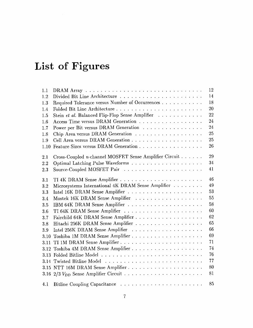
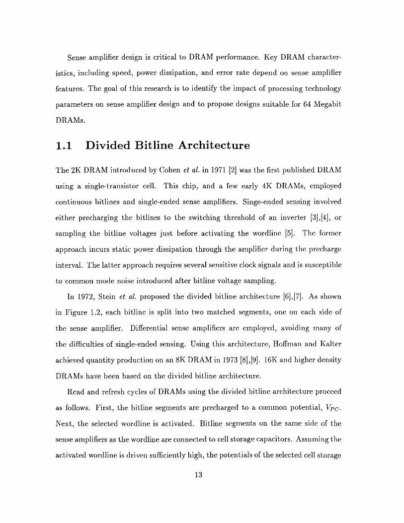
shown in Figure 1.1, each cell comprises a single access transistor and a single storage
capacitor. Binary information is represented by the state of the storage capacitors.
Each cell holds a single bit. Typically, a high stored potential represents a '1' and a
low stored potential represents a '0'. Cells must be periodically refreshed to prevent
loss of data due to charge leakage.
Wordlines connect the access transistor gates of each cell row. Activating a word-
line turns on the access transistors, connecting the cell storage capacitors to bitlines.
Data may then be read from or written to the cells through the bitlines. Each bitline
serves a column of cells. Deactivating the wordline isolates the storage capacitors
from the bitlines.
Before activating a wordline to read or refresh a cell row, the bitlines are precharged
to a common potential. Activation of the wordline causes charge sharing to occur
between cell storage capacitors and bitlines. Small signals reflecting cell states are
produced on each bitline. The signals must be amplified, and the original state of
the storage capacitors must be restored. These functions are performed by sense
amplifiers.
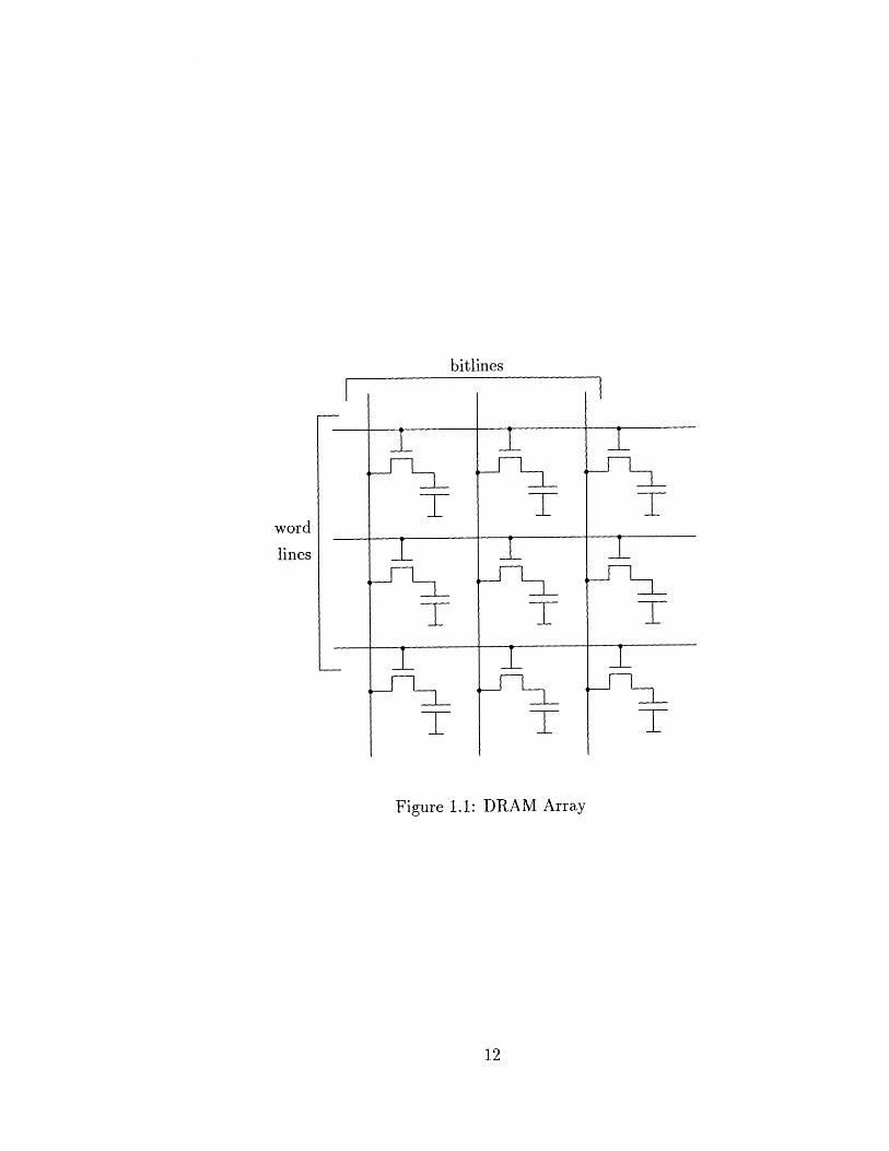
bitlines
T T T
T T T
I I
T T
Figure 1.1: DRAM Array
word
lines
Sense amplifier design is critical to DRAM performance. Key DRAM character-
istics, including speed, power dissipation, and error rate depend on sense amplifier
features. The goal of this research is to identify the impact of processing technology
parameters on sense amplifier design and to propose designs suitable for 64 Megabit
DRAMs.
1.1 Divided Bitline Architecture
The 2K DRAM introduced by Cohen et al. in 1971 [2] was the first published DRAM
using a single-transistor cell. This chip, and a few early 4K DRAMs, employed
continuous bitlines and single-ended sense amplifiers. Singe-ended sensing involved
either precharging the bitlines to the switching threshold of an inverter [3],[4], or
sampling the bitline voltages just before activating the wordline [5]. The former
approach incurs static power dissipation through the amplifier during the precharge
interval. The latter approach requires several sensitive clock signals and is susceptible
to common mode noise introduced after bitline voltage sampling.
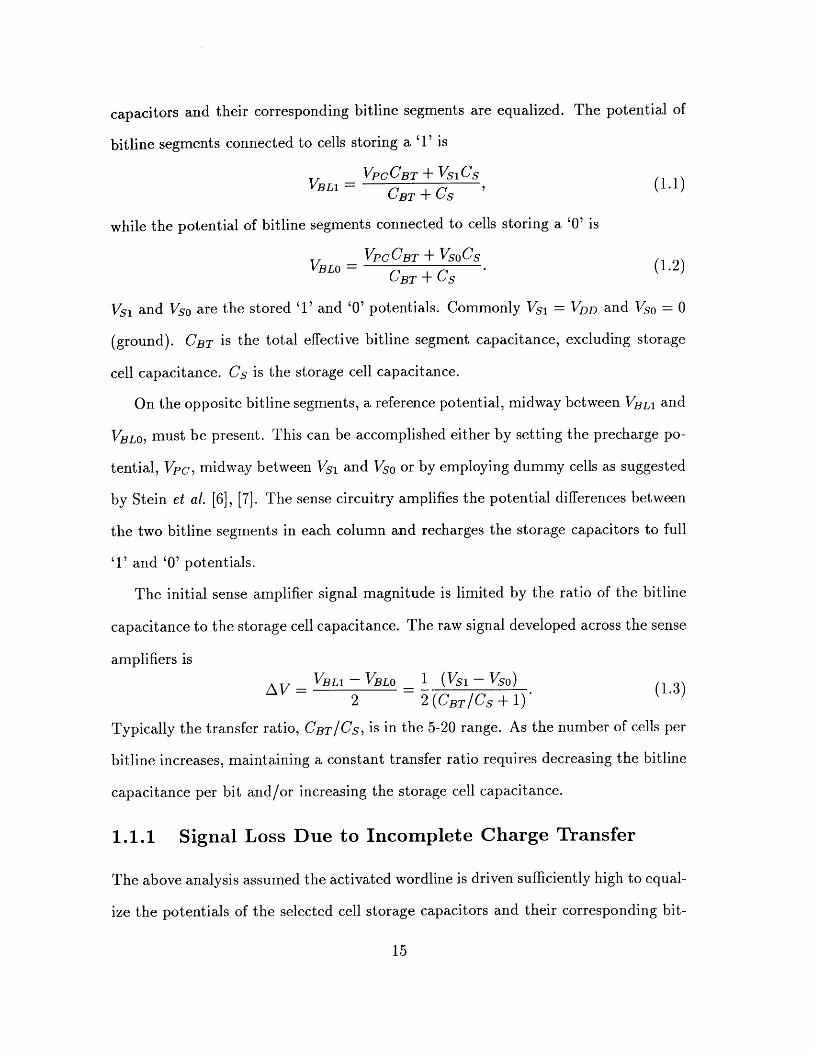
In 1972, Stein et al. proposed the divided bitline architecture [6],[7]. As shown
in Figure 1.2, each bitline is split into two matched segments, one on each side of
the sense amplifier. Differential sense amplifiers are employed, avoiding many of
the difficulties of single-ended sensing. Using this architecture, Hoffman and Kalter
achieved quantity production on an 8K DRAM in 1973 [8],[9]. 16K and higher density
DRAMs have been based on the divided bitline architecture.
Read and refresh cycles of DRAMs using the divided bitline architecture proceed
as follows. First, the bitline segments are precharged to a common potential, Vpc.
Next, the selected wordline is activated. Bitline segments on the same side of the
sense amplifiers as the wordline are connected to cell storage capacitors. Assuming the
activated wordline is driven sufficiently high, the potentials of the selected cell storage

bitlines
sense sense sense senseamp amp amp amp
Figure 1.2: Divided Bit Line Architecture
wordlines
i Rom -MAR&WWW.-
capacitors and their corresponding bitline segments are equalized. The potential of
bitline segments connected to cells storing a '1' is
VPCCBT + VS1 0SVBL1 -B+S 11
CBT + CS
while the potential of bitline segments connected to cells storing a '0' is
VPCCBT + VSOCSCBT + CS
Vsi and VSo are the stored '1' and '0' potentials. Commonly Vs1 = VDD and Vso = 0
(ground). CBT is the total effective bitline segment capacitance, excluding storage
cell capacitance. CS is the storage cell capacitance.
On the opposite bitline segments, a reference potential, midway between VBL1 and
VBLO, must be present. This can be accomplished either by setting the precharge po-
tential, Vpc, midway between Vs1 and VSo or by employing dummy cells as suggested
by Stein et al. [6], [7]. The sense circuitry amplifies the potential differences between
the two bitline segments in each column and recharges the storage capacitors to full
'1' and '0' potentials.
The initial sense amplifier signal magnitude is limited by the ratio of the bitline
capacitance to the storage cell capacitance. The raw signal developed across the sense
amplifiers is
AV = VBL1 - VBLO _ (VS1 - VSO) (1.3)2 2 (CBTCS + 1)
Typically the transfer ratio, CBTICS, is in the 5-20 range. As the number of cells per
bitline increases, maintaining a constant transfer ratio requires decreasing the bitline
capacitance per bit and/or increasing the storage cell capacitance.
1.1.1 Signal Loss Due to Incomplete Charge Transfer
The above analysis assumed the activated wordline is driven sufficiently high to equal-
ize the potentials of the selected cell storage capacitors and their corresponding bit-
15
line segments. In some DRAM designs, this assumption is invalid. For example, if
VSO = 0, VPC = VDD and the wordline is not driven above VDD during signal develop-
ment, n-channel transfer devices accessing a stored '0' will shut off when the storage
cell potential reaches VDD - VT, where VT is the transfer device threshold voltage.
Equations (1.1), (1.2), and (1.3) can be modified to encompass cases involving
incomplete equalization. After signal development is complete, the potential of bitline
segments connected to cells storing a '1' is
VPCCBT + vS1CS - (VC1 - VBL1)CSVBL1 =14) CBT+C S
where Vci is the final potential of the '1' storage cells. The potential of bitline
segments connected to cells storing a '0' is
VPCCBT + VSOCS - (V0O - VBLO)CSVBL0 = CB S(1.5)
CBT+&CS
where Vco is the final potential of the '0' storage cells. Thus, the raw signal developed
across the sense amplifiers is
1 (VS1 - VS0 ) - (VC1 - VBL1 - (VBLO - V00 )AV = (CTC±). (1.6)2 (CBTICS + 1)
1.1.2 Dummy Storage Cells
Unless the bitline precharge potential is midway between VBL1 and VBLO, dummy
cells must be used. A single row of dummy cells is placed on each side of the sense
amplifier. The basic structure of the dummy cells is identical to the normal storage
cell structure. Dummy wordlines connect the access transistor gates of each dummy
cell row. The dummy storage capacitors are precharged to a common potential. When
the selected wordline is activated, the dummy wordline on the opposite side of the
sense amplifier is also activated.

The dummy storage capacitor precharge potential and capacitance are designed
to produce the proper bitline segment reference potential. Two schemes are com-
mon. In the first scheme, the dummy cell capacitance is equal to the normal storage
cell capacitance. The dummy storage capacitors are precharged to a potential mid-
way between Vs1 and Vso. In the other arrangement, the bitlines are precharged to
Vsi. The dummy cell capacitors, with about one-half the capacitance of the normal
storage cell capacitors, are precharged to Vso. When the wordline and dummy word-
line are activated, the potentials of bitline segments connected to cells storing a '1'
remain at Vsi. The potentials of segments connected to cells storing a '0' drop to
VsiCBT/(CBT + Cs). The potentials of segments connected to dummy cells drop to
Vs1CBT/ 2(CBT + CS)-
The first scheme allows use of any bitline precharge potential but requires precharg-
ing the dummy storage cell capacitors to an intermediate potential. A dummy cell
precharge voltage generator may be needed. The second scheme constrains the bitline
precharge potential and requires a unique dummy storage cell capacitance. It also
creates an imbalance in the bitline segment node capacitances during sensing.
1.2 Noise Sources
A wide variety of phenomena, commonly referred to as "noise sources," may degrade
signals presented to the sense amplifiers. Equations (1.3) and (1.6) do not account
for these phenomena. Yet the noises produced are often of such magnitude that they
may not be safely neglected.
Bitline, storage cell, and dummy cell capacitance variations alter the bitline po-
tentials produced by signal development. Process tolerances and mismatches must
both be considered. Capacitances may vary both globally, from chip to chip, and
locally, from cell to cell or bitline to bitline.
6.5a +
6.0 --99.9% 9%
-.5 5%a 5.5 --
Cr
0
Er 4.5 -
3.5or
3.5cr3.0O | ' ' I I I '
64 1K 16K 256K 4M 64MNumber of Occurrences
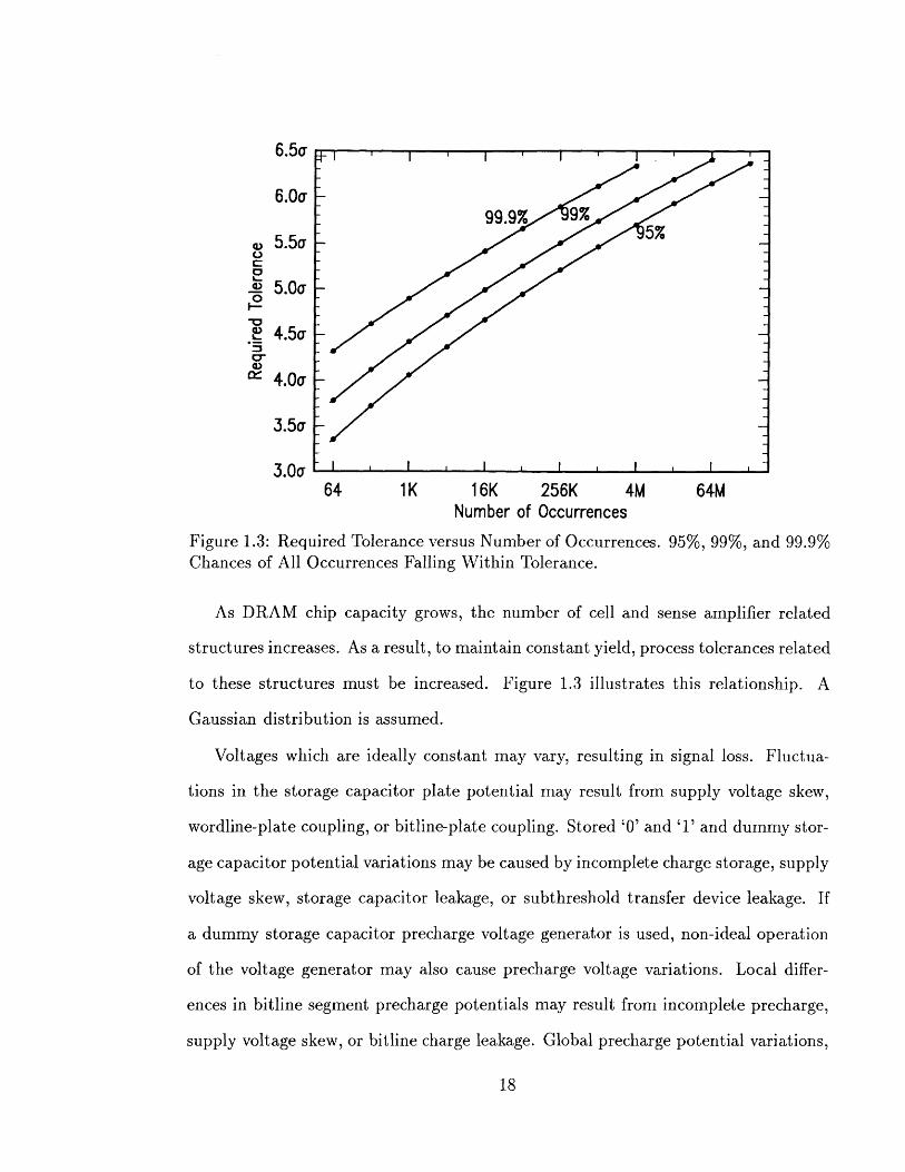
Figure 1.3: Required Tolerance versus Number of Occurrences. 95%, 99%, and 99.9%Chances of All Occurrences Falling Within Tolerance.
As DRAM chip capacity grows, the number of cell and sense amplifier related
structures increases. As a result, to maintain constant yield, process tolerances related
to these structures must be increased. Figure 1.3 illustrates this relationship. A
Gaussian distribution is assumed.
Voltages which are ideally constant may vary, resulting in signal loss. Fluctua-
tions in the storage capacitor plate potential may result from supply voltage skew,
wordline-plate coupling, or bitline-plate coupling. Stored '0' and '1' and dummy stor-
age capacitor potential variations may be caused by incomplete charge storage, supply
voltage skew, storage capacitor leakage, or subthreshold transfer device leakage. If
a dummy storage capacitor precharge voltage generator is used, non-ideal operation
of the voltage generator may also cause precharge voltage variations. Local differ-
ences in bitline segment precharge potentials may result from incomplete precharge,
supply voltage skew, or bitline charge leakage. Global precharge potential variations,

important in designs not employing dummy cells, may be caused by supply voltage
skew or, if a bitline precharge voltage generator is employed, non-ideal operation of
the voltage generator.
Injection of minority carriers into the bulk region of the array may cause signal
loss. Charge injection can occur as a result of alpha particle radiation or chip input
undershoot or overshoot. Injected charge collected by cell storage capacitors may
alter the stored potentials. In addition, during signal development injected charge
may be collected by the bitline segments, altering the bitline potentials.
Electrical coupling within the array affects signal development. Changes in word-
line potential can result in storage cell state-dependent changes in bitline and storage
capacitor potentials. Bitline to bitline coupling results in pattern-dependent effective
bitline capacitance changes. Bitline potential changes during signal development may
induce changes in wordline, bulk, or plate potentials. These changes may, in turn,
alter the bitline potentials.
1.3 Folded Bitline Architecture
In the conventional divided bitline arrangement shown in Figure 1.2, matched bitline
segments extend from opposite sides of the sense amplifiers. This arrangement is used
in most 16K DRAMs. The folded bitline architecture, shown in Figure 1.4, is used
in many 64K and higher density DRAMs. It requires a more complex cell structure,
but offers several advantages over the conventional open bitline architecture.
With open bitlines, differential column I/O sensing requires placement of column
decode circuits between the sense amplifiers and the array. Use of folded bitlines
allows placement of column decode circuitry at the ends of the bitlines, reducing
bitline capacitance and eliminating coupling between the bitlines and the column
address lines [10], [11], [12].

wordlines
bit-
lines
sense
amp
Figure 1.4: Folded Bit Line Architecture
The folded bitline architecture reduces the sense amplifier pitch constraint from
one bitline segment pitch to two bitline segment pitches. In many cases, this may
allow more efficient sense amplifier layout [13].
Employing folded bitlines may help improve noise rejection. Some mechanisms
which introduce differential mode noise in open bitline designs may produce only
common mode noise in folded bitline configurations [14], [15].
The folded bitline architecture reduces the physical distance between paired bitline
segments. Thus folded arrays are, in general, less sensitive to spatial bulk and plate
potential variations. In addition, during signal development, roughly equal amounts
of injected charge may be collected by neighboring bitline segments. Thus, charge
injection during signal development may produce smaller changes in potential between
paired bitline segments in a folded bitline arrangement.
sense
amp

In open bitline configurations, the average bitline potential change in each storage
cell array is highly dependent on the stored pattern. In most folded configurations,
the average bitline potential change is independent of the stored pattern. Thus, in
a folded bitline architecture, differential plate, bulk, and wordline potential changes
resulting from coupling to bitlines may be reduced.
1.4 Balanced Flip-Flop Sense Amplifier
The differential sense amplifiers used in modern DRAMs are variations of the balanced
flip-flop sense amplifier presented by Stein et al. in 1972 [6],[7]. The circuit is shown
in Figure 1.5. During the precharge period #1 and 02 are high, 42 is low, and both
dummy wordlines are activated. The bitline and dummy cell potentials are set to the
switching threshold of the flip-flop. After the precharge voltage is established, 41 and
02 go low, 2 goes high, and the dummy wordlines are deactivated. When a wordline
is activated, the dummy wordline on the opposite side of the sense amplifier is also
activated. Offset introduced by capacitive coupling of bitline segments to the active
wordline is compensated by coupling of the opposite segments to the active dummy
wordline. Driving 0 2 high and 02 low activates the flip-flop, initiating sense signal
amplification. The lower potential bitline segment is discharged through one of the
cross-coupled transistors. The higher potential segment is pulled up through one of
the load transistors.
In 16K and higher density DRAMs, sense amplifier performance is improved by
keeping static load transistors off during signal amplification and by driving the source
of the cross-coupled pair slowly during initial sensing as suggested by Lynch and Boll
[16]. If static load transistors are activated at the same time as the cross-coupled de-
vice pair, current flows through a load device into the lower potential bitline segment,
unproductively dissipating power. In addition, the load device current going into the
MM dNN(N-_.
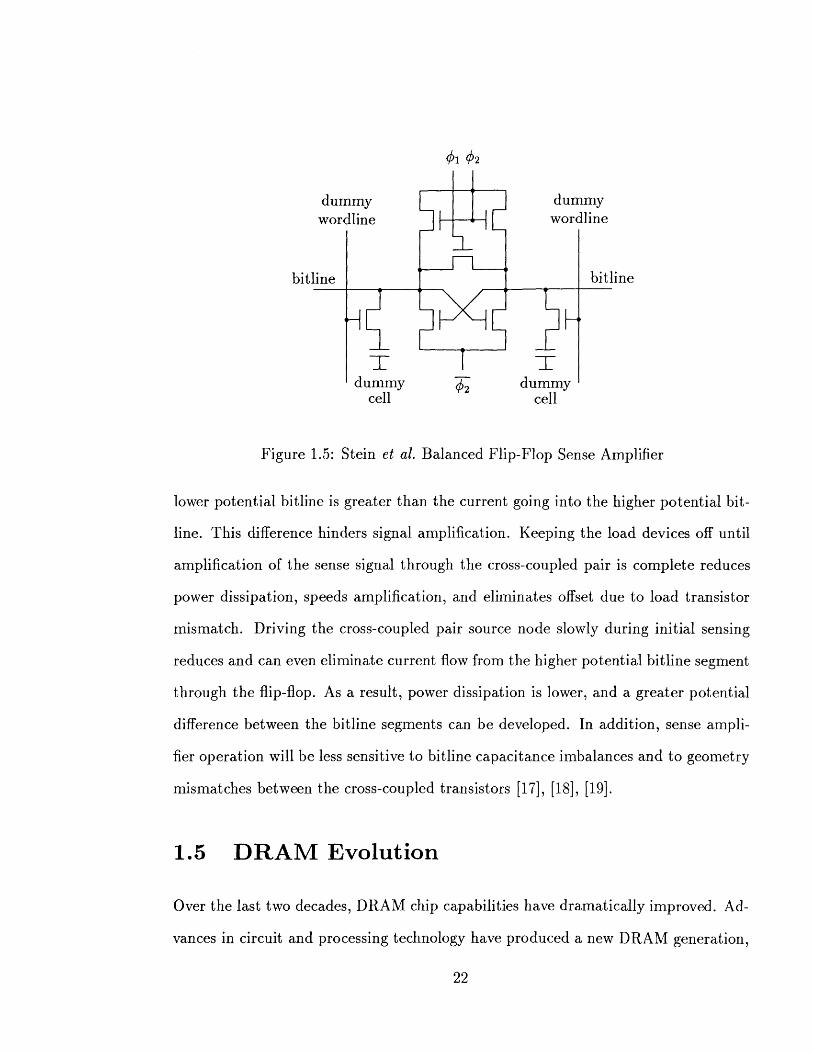
91 02
dummy dummywordline wordline
bitline bitline
dummy ~2 dummycell cell
Figure 1.5: Stein et al. Balanced Flip-Flop Sense Amplifier
lower potential bitline is greater than the current going into the higher potential bit-
line. This difference hinders signal amplification. Keeping the load devices off until
amplification of the sense signal through the cross-coupled pair is complete reduces
power dissipation, speeds amplification, and eliminates offset due to load transistor
mismatch. Driving the cross-coupled pair source node slowly during initial sensing
reduces and can even eliminate current flow from the higher potential bitline segment
through the flip-flop. As a result, power dissipation is lower, and a greater potential
difference between the bitline segments can be developed. In addition, sense ampli-
fier operation will be less sensitive to bitline capacitance imbalances and to geometry
mismatches between the cross-coupled transistors [17], [18], [19].
1.5 DRAM Evolution
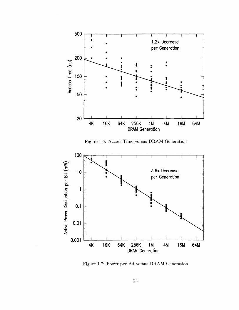
Over the last two decades, DRAM chip capabilities have dramatically improved. Ad-
vances in circuit and processing technology have produced a new DRAM generation,

with 4x greater chip capacity, every 2-4 years. 4M DRAMs are now in production. As
shown in Figure 1.6, access time has gradually improved. Large decreases in power
dissipation per bit, shown in Figure 1.7, have limited increases in chip power.
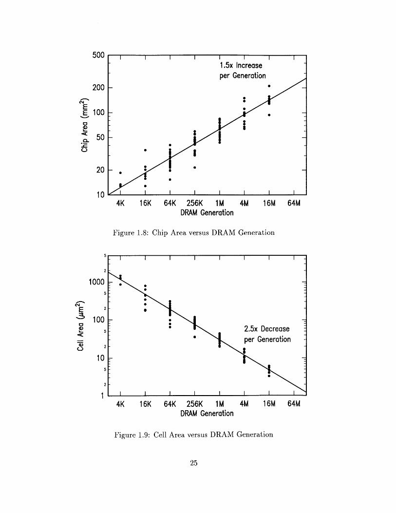
Increased chip capacity has been achieved primarily by decreasing cell size and
increasing chip area. As shown in Figure 1.8, chip area has increased approximately
1.5x per generation. Cell area decreased by approximately 2.5x per generation as
shown in Figure 1.9. Together, these two trends account for over 90% of the increase
in chip capacity with each generation.
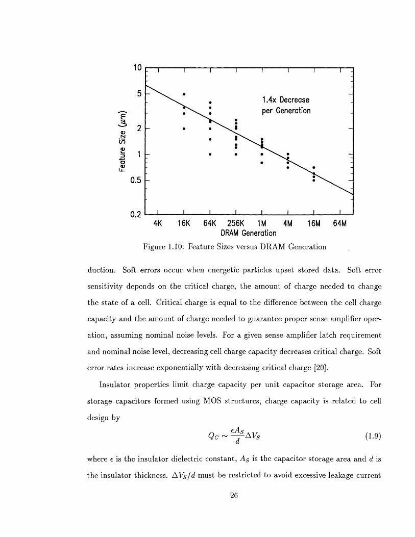
The decrease in cell area has been obtained by reducing feature sizes and by
employing new cell structures. As shown in Figure 1.10, feature sizes have been
reduced by about 1.4x per generation. This reduction accounts for a 2.1x reduction
in cell area per generation. The remaining 1.2x cell area reduction has been produced
through cell structure innovation.
The need to preserve charge capacity constrains cell evolution. Charge capacity is
the difference in stored charge between '0' and '1' cell capacitor states, and is given
by
Qc=vsI Cs(Vs) dVs ~ Cs AVs (1.7)
where AVs is the potential difference between stored '0' and '1' levels. Maximum
sense signal magnitude is related to charge capacity by
AV 1 Qo 1lOcA V =I - ~l_ --Q (1.8)2 CBT + CS 2 CBT
As chip capacity increases, decreases in bitline capacitance per bit are generally ac-
companied by increases in the number of cells per bitline. As a result, bitline segment
capacitance remains roughly constant. Thus, charge capacity must be conserved in
order to maintain adequate sense signal magnitude.
Particle-induced soft error rate considerations also discourage charge capacity re-
S~- -~-
4K 16K 64K 256K 1M 4M 16M 64MDRAM Generation
Figure 1.6: Access Time versus DRAM Generation
4K 16K 64K 256K 1M 4M 16M 64MDRAM Generation
Figure 1.7: Power per Bit versus DRAM Generation
500
200
100
50
100
E%--
l.
0
0
-
0n
0
10
1
0.1
0.01
0.001
4K 16K 64K 256K 1M 4M 16M 64MDRAM Generation
Figure 1.8: Chip Area versus DRAM Generation
4K 16K 64K 256K 1M 4M 16M 64MDRAM Generation
Figure 1.9: Cell Area versus DRAM Generation
500
200
100
50
10005
2
100
EE
0-
c.~I
E3
0a)1~
0
10
501.4x Decreaseper Generation
E
17
0.5
0.24K 16K 64K 256K 1M 4M 16M 64M
DRAM Generation
Figure 1.10: Feature Sizes versus DRAM Generation
duction. Soft errors occur when energetic particles upset stored data. Soft error
sensitivity depends on the critical charge, the amount of charge needed to change
the state of a cell. Critical charge is equal to the difference between the cell charge
capacity and the amount of charge needed to guarantee proper sense amplifier oper-
ation, assuming nominal noise levels. For a given sense amplifier latch requirement
and nominal noise level, decreasing cell charge capacity decreases critical charge. Soft
error rates increase exponentially with decreasing critical charge [20].
Insulator properties limit charge capacity per unit capacitor storage area. For
storage capacitors formed using MOS structures, charge capacity is related to cell
design by
Qc ~ AVs (1.9)u d
where c is the insulator dielectric constant, As is the capacitor storage area and d is
the insulator thickness. AVs/d must be restricted to avoid excessive leakage current
4K 16Kplanar cell planar cellmetal wordlines metal wordlinesdiffused bitlines diffused bitlinessingle-level poly double-level poly
64K 256Kplanar cell Hi-C planar cellpoly Si wordlines polycide wordlinesmetal bitlines metal bitlinesdouble-level poly double-level poly
iM 4M,16MHi-C planar cell trench or stacked1/2 VDD plate capacitor cellpoly Si wordlines poly Si wordlinesmetal bypass wordlines metal bypass wordlinespolycide bitlines polycide bitlinestriple-level poly
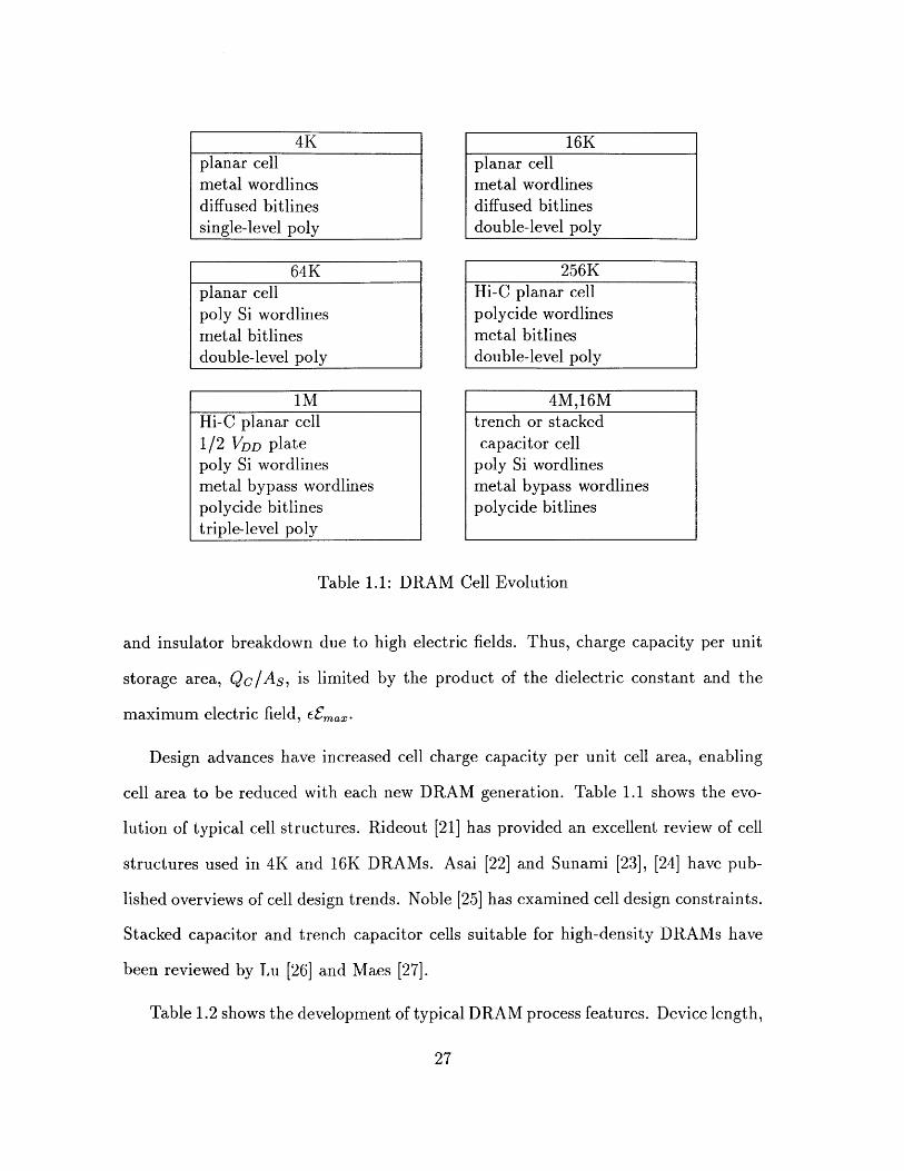
Table 1.1: DRAM Cell Evolution
and insulator breakdown due to high electric fields. Thus, charge capacity per unit
storage area, Qc/As, is limited by the product of the dielectric constant and the
maximum electric field, .max.
Design advances have increased cell charge capacity per unit cell area, enabling
cell area to be reduced with each new DRAM generation. Table 1.1 shows the evo-
lution of typical cell structures. Rideout [21] has provided an excellent review of cell
structures used in 4K and 16K DRAMs. Asai [22] and Sunami [23], [24] have pub-
lished overviews of cell design trends. Noble [25] has examined cell design constraints.
Stacked capacitor and trench capacitor cells suitable for high-density DRAMs have
been reviewed by Lu [26] and Maes [27].
Table 1.2 shows the development of typical DRAM process features. Device length,
I
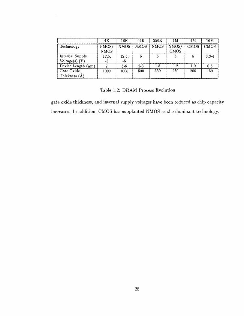
4K 16K 64K 256K 1M 4M 16MTechnology PMOS/ NMOS NMOS NMOS NMOS/ CMOS CMOS
NMOS CMOS
Internal Supply 12,5, 12,5, 5 5 5 5 3.34Voltage(s) (V) -3 -5
Device Length (pm) 7 5-6 2-3 1.5 1.2 1.0 0.6Gate Oxide 1000 1000 500 350 250 200 150Thickness (A)
Table 1.2: DRAM Process Evolution
gate oxide thickness, and internal supply voltages have been reduced as chip capacity
increases. In addition, CMOS has supplanted NMOS as the dominant technology.
N
Chapter 2
Theoretical Analysis of SenseAmplifier Operation
Theoretical analysis of the sensing operation is useful for understanding circuit per-
formance. While computer simulation may provide more precise results, theoretical
analysis gives a much clearer picture of design and process parameter influences.
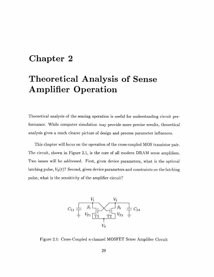
This chapter will focus on the operation of the cross-coupled MOS transistor pair.
The circuit, shown in Figure 2.1, is the core of all modern DRAM sense amplifiers.
Two issues will be addressed. First, given device parameters, what is the optimal
latching pulse, Vs(t)? Second, given device parameters and constraints on the latching
pulse, what is the sensitivity of the amplifier circuit?
CLT
Figure 2.1: Cross-Coupled n-channel MOSFET Sense Amplifier Circuit

The following first-order MOS transistor current expressions will be used:
#(VGS - VT - IVDS)VDS, VDS! VGS - VT
IDS = (2.1){#(VGS -T) 2 . VDS > VGS - VT
VGS is the gate-source voltage, VDS is the drain-source voltage, and VT is the threshold
voltage. # is the transistor gain factor and is given by
W# = L peffCox (2.2)
where W and L are the transistor lengths and widths, respectively, pe5f is the effective
channel mobility, and C0 x is the gate oxide capacitance per unit area.
2.1 Latching Pulse Optimization
Sense amplifier performance depends on characteristics of the latching pulse, V(t).
Following the analysis of Lynch and Boll [16], the optimal latching pulse will be
derived, given the constraint that no current may flow through the "off-side" (T2) of
the flip-flop. Perfect matching will be assumed, giving
(WIL) = (W/L)1 = (W/L) 2, #3 =01 = 02' (2.3)VT = VT = VT 2 , CL L1 = CL2-
Gate-source capacitances will be neglected for VGS < VT. They will be assumed
constant for VGS > VT. A constant, Cc, will be used to model the capacitance
between the two signal nodes. Variations in threshold voltages with device operating
points will be ignored.
Prior to the start of the sensing operation, V1 = V and V2 = V + v, where v is
the magnitude of the signal presented to the amplifier. Vs > Vo - VT + v, keeping
both TI and T2 off. Amplification begins, at t = 0, when the latch node potential,
VS, is driven below V - VT + v, turning on TI.
To maximize sensing speed, Vs should decrease as quickly as possible. Preventing
off-side conduction requires V - Vs 5 VT. Thus, maximum sensing speed without
off-side conduction is achieved when
Vs(t) = V(t) - VT. (2.4)
Initially, the optimal latching pulse is a negative step to V - VT. T1 will conduct,
reducing V1. Vs should decrease with V1 , always keeping T2 marginally off. As Vs
decreases, the overdrive on T1 increases, and consequently V1 decreases more rapidly.
Thus, after the initial step, Vs will decrease at a progressively increasing rate.
Though T2 is always kept off, V2 decreases as a result of capacitive coupling
between the two signal nodes and TI gate-source coupling. For V2 - Vs > VT, charge
conservation requires
(Vo + v)CL + vCc = V2 (t)CL + [V2(t) - Vi(t)]Cc + [V2 (t) - Vs(t) - VT]CGS (2.5)
where CGS is the gate-source capacitance. Using (2.4) in this expression gives an
equation for V2 (t):
V2 (t) = Vs(t) + VT + f1 [V - Vs(t) - VT] + f2v (2.6)
where
CL _ CL+CCfi C CC+ and f2 CL .+C (2.7)CL + CC + CGS -CL + CC + CGS'
Assigning t = 0 at the instant immediately before Vs begins decreasing, the node
potentials at t = 0+, immediately after the negative Vs step, are given by
V(0+) = VOV2(0+) = VO + f2V (2.8)Vs(0+) = VO -VT.
While V1 > V2 - VT, Ti operates in the saturation regime and
dV1 (t) [dV(t) dV2 (t) 1 V 2.-C - -t dt =~[V2 (t) ~VS(t)-dt dt dt 2
Using (2.4) and (2.6) in (2.9) gives a differential equation for Vs(t):
dVs(t)- (CL + f1Cc) dt
P{ fl[Vo -Vs(t) - VT] + f 2v}2.2
The solution to (2.10) with the initial condition given by (2.8) is
Vs(t ) = V0 - VT -[1//2(CL + f1CC)]f 2
2v 2t
1 - [!/2(CL + fiCC)]fif 2vt
Equation (2.11) is valid until, at t = tat, Ti goes into the linear operation regime.
tsat is defined by
V(tsat) = V2 (tsat) - VT. (2.12)
Using (2.4), (2.6), and (2.11) in (2.12) gives
sat2(CL + f1Cc) (VT - f 2 v )
n (2f1 f2. V
Substituting (2.13) in (2.11) gives
2(CL + 2Cc + CGs) (VT - f2v)
#f 2v VT
1Vs(t sat) VO VT (Vr -f2 V).
fi
(2.13)
(2.14)
Once T1 is operating in the linear regime
dVs(t )-(CL + f1Cc) dt =fJ{V2 (t) - VS(t) - VT - V1(t) - Vs(t )1t) - VS(21-
(2.15)
Using (2.4) and (2.6) in (2.15) gives a differential equation for Vs(t):
fC)dVs(t)-(CL + 1 dt #VT {f[VO - VS~t -VT] + f2v -
The solution to this equation with the initial condition given by (2.14) is
VS(t) = V - VT - -(VT - f2v) + 1 - expfi 2f1
[f1VT(t -tsat)CL + fiCo
The latch node potential rapidly falls according to (2.17) until Vs reaches ground.
At this point the sensing operation can be considered complete. V2 will remain
(2.10)
(2.11)
(2.16)
(2.17)
avg.
POP.
constant while V1 decreases towards ground.
tsense, is defined by
VS(tsense) = 0. (2.18)
Substituting (2.17) in (2.18) gives
Ctsat - L + fiCC nOf1 VT E 2f1(Vo -
VT) - VT + 2f 2 vVT ~ I
(2.19)
After VS reaches ground, conduction through TI continues pulling V towards
ground. The final node potentials are given by
V (final) = 0V2 (final) = fiVo + f 2 v + (1 - f 2 ) VTVs(final) = 0.
(2.20)
The total reduction of the high signal node potential, V2, resulting from the sensing
operation is given by
CC + CGS CGSAV2[coupling] = VC - (VT - v)
CL + CC + CGS CL + CC + CGS(2.21)
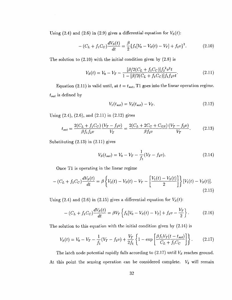
Examples of optimal VS(t) waveforms are shown in Figure 2.2. Since, for practical
parameter values, tsense ~ t,, several conclusions may be drawn from (2.13) and
(2.21):
* for CGS < CL + CC, tsense is approximately proportional to (CL + 2Cc + CGS);
e tsense is approximately inversely proportional to the transistor gain factor, #;
" for v < VT/f 2, tsense is approximately inversely proportional to the initial signal,
v; and
* for Vo > (VT - v), AV2/ V2 (initial) is approximately equal to (CC + CGS) /(CL +
CC + CGS)-
The length of the sensing operation,
C
0
~0
0
.c
3.0
2.5
2.0
1.5
1.0
0.5 -
0.00 5 10 15 20
Time (ns)Figure 2.2: Optimal Latching Pulse Waveforms
Sensing speed can be increased by allowing off-side conduction. The consequence
of off-side conduction is a reduction of the final voltage of the higher potential signal
node, V2. Lynch and Boll [16] derived expressions for the optimal latching pulse
assuming constant off-side current. Their analysis shows that tat is given by
CLtsat = l In
Of VCVT
VT+ 2Vc
fv+2V
fv I(2.22)
where
CL
CL + CGS(2.23)
Vc is the constant gate-source overdrive of transistor T2. Signal node coupling was
neglected.
If VC < 5fv and Vc < VT
- fv+2Vc
~ 2 IfI fv+2Vc + 1I. fvj
-2 2 Vc2fv + 2Vc
ln VT1VT + 2Vc
fv + 2Vc]
fV(2.24)

Using this equation in (2.22) gives
2CLtsat ~ + for Vc < 5fv and Vc < VT. (2.25)tstr"#f (fo + VC)
Comparing this equation and (2.13) shows that for small off-side conduction levels,
the effect of increasing Vc on the length of the optimal latching pulse is similar to
the effect of increasing the initial signal v. The reduction in the final voltage of the
higher signal node potential due to off-side conduction is given by
. 3VCstsense Cfcst_ _
AV2[conduction] = 2(CL + .GS) e 2 ta (2.26)
Substitution of (2.25) into (2.26) gives
V02
AV2 [conduction] (fv C for Vc < 5fv and Vc < VT. (2.27)
For low conduction levels, the reduction in the final high signal potential is less than
the "off" transistor overdrive, VC. Thus, significant increases in sensing speed can be
achieved with only small reductions in the final high signal potential. For example,
sensing with Vc = v is approximately two times faster than sensing without off-side
conduction. Yet the additional drop in the final high signal potential is less than v.
2.2 Sensitivity
One of the most important sense amplifier performance characteristics is sensitivity.
Loosely defined, the sensitivity is the minimum detectable signal presented to the
sense amplifier. Natori [28] more precisely defines the sensitivity as the minimum
initial signal, v, needed to insure that the resulting drop in the final high-level signal
node potential due to off-side conduction, AV 2, will not prevent correct subsequent
circuit operation.
Sense amplifier sensitivity may be characterized by two components, offset and
minimum overdrive. The offset voltage is the initial signal which results in precisely
equal signal node potential changes during amplifier operation. The offset voltage of
a perfectly balanced sense amplifier is zero. The minimum overdrive voltage is the
minimum difference between the initial signal and the offset voltage needed to insure
that the final high-level signal node potential will permit correct subsequent circuit
operation. Sensitivity can be expressed as
VS = VOS + VOD,min (2.28)
where vOs is the offset voltage and VOD,min is the minimum overdrive voltage.
Because the sensing operation outcome depends on the shape of the latching pulse,
Vs(t), and the initial signal, v, characterization of sensitivity is very difficult. In what-
ever manner the problem is addressed, simplifying assumptions must be employed to
make the analysis tractable. For any single approach, the assumptions required cast
significant doubt on the general validity and applicability of the solution. However,
by examining the results of several different analyses, some important conclusions can
be made with a good degree of confidence.
Sensitivity will be examined in the following manner. First, the physical origins
of electrical mismatches will be summarized. Then, the results of published analyses
will be reviewed. Next, sense amplifier sensitivity will be related to the dc offset
voltage of the MOS source-coupled pair. Finally, some general conclusions will be
presented.
2.2.1 Sense Amplifier Circuit Mismatches
Sensitivity is commonly characterized using electrical mismatch parameters AVT, A/3,
ACL, and ACGS. These parameters are defined by the following expressions:
V1T = VT + AVT/2, VT2 = VT - AVT/2,
#1= - A#/2, #2 = #+ A0/2,CL1 CL + ACL/2, 0 L2 = CL ~ ACL/2(
CGs = CGs + ACGs12, CGS2 = Cs -ACGs12.
WINa - I
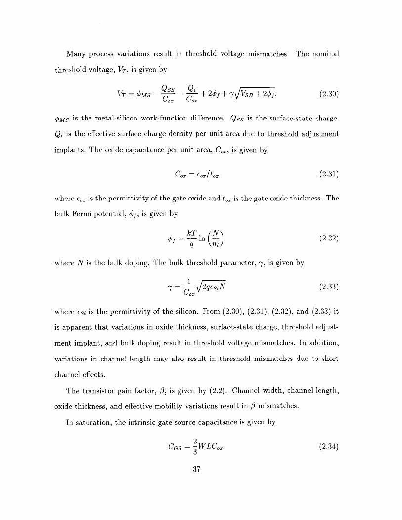
Many process variations result in threshold voltage mismatches. The nominal
threshold voltage, VT, is given by
VT = #us - Css Ci + 2#f + 7 VSB + 20f (2.30)
qMS is the metal-silicon work-function difference. Qss is the surface-state charge.
Q; is the effective surface charge density per unit area due to threshold adjustment
implants. The oxide capacitance per unit area, Cox, is given by
Cox = cox/to0 (2.31)
where cox is the permittivity of the gate oxide and to0 is the gate oxide thickness. The
bulk Fermi potential, of, is given by
f -=U In - (2.32)q (ni
where N is the bulk doping. The bulk threshold parameter, y, is given by
17 = 2qes;N (2.33)
where eSi is the permittivity of the silicon. From (2.30), (2.31), (2.32), and (2.33) it
is apparent that variations in oxide thickness, surface-state charge, threshold adjust-
ment implant, and bulk doping result in threshold voltage mismatches. In addition,
variations in channel length may also result in threshold mismatches due to short
channel effects.
The transistor gain factor, 3, is given by (2.2). Channel width, channel length,
oxide thickness, and effective mobility variations result in # mismatches.
In saturation, the intrinsic gate-source capacitance is given by
2CGS = -WLCox. (2.34)
3
Thus, device width, device length, and oxide thickness variations result in CGS mis-
matches.
The total signal node to ground capacitance, CL, includes capacitances in the
sense amplifier, and unless the bitlines are completely isolated from the sense am-
plifier during sensing, capacitances in the storage cell array. A major component of
the sense amplifier contribution is the depletion region capacitances between the bulk
and drain regions of the cross-coupled devices. Bulk doping variations result in CL
mismatches. In addition, misalignment of gate and diffusion masks may create differ-
ences in cross-coupled device drain areas, resulting in capacitance mismatches. The
array contribution to the signal node to ground capacitance is subject to mismatches
due to a variety of process variations including differences in transfer device diffusion
capacitance, differences in isolation thickness, and differences in bitline width and
height.
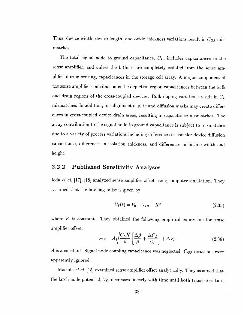
2.2.2 Published Sensitivity Analyses
Ieda et al. [17], [18] analyzed sense amplifier offset using computer simulation. They
assumed that the latching pulse is given by
Vs(t) =VO -VT 2 - Kt (2.35)
where K is constant. They obtained the following empirical expression for sense
amplifier offset:
CL+a ACLI+ATvos=A [ + L+Av. (2.36)
A is a constant. Signal node coupling capacitance was neglected. CGS variations were
apparently ignored.
Masuda et al. [15] examined sense amplifier offset analytically. They assumed that
the latch node potential, Vs, decreases linearly with time until both transistors turn
on. Once both transistors begin conducting, the latch node potential was assumed to
decrease in such a manner that the low signal node potential, V1, decreases linearly
with time according to
dV2 (t) = aK (2.37)dt
where a and K are constants. They derived the following expression for sense ampli-
fier offset:
CLaK 11- ACLCos- + + AV. (2.38)V20 10 CL
Signal node coupling capacitance and gate-source capacitances were apparently ig-
nored.
Kraus [29] also examined sense amplifier offset analytically. Like Ieda et al. , he
assumed that the latch node potential decreases linearly with time:
Vs Vs(O) - kt. (2.39)
He obtained the following expression for sense amplifier offset:
~ V 2CLlk 2CL2 kVos ed A T + -; . ( 2.40 )
Signal node coupling capacitance and gate-source capacitances were apparently ig-
nored. If Ap/# < 1 and ACL/CL < 1 this expression reduces to
CLK_ A3 AOL (.1vos e AVT + A + (2.41)
V2# CL)
Natori [28] derived a general expression for sensitivity. He began by deriving
expressions for the optimal latching pulse assuming constant off-side current. He
observed that the variations in optimal Vs(t) waveforms are mostly due to changes in
tsat. Arbitrary Vs(t) waveforms, he argued, can be characterized by one parameter,
tsat, and therefore matched with an optimal Vs(t) waveform. Using results of his
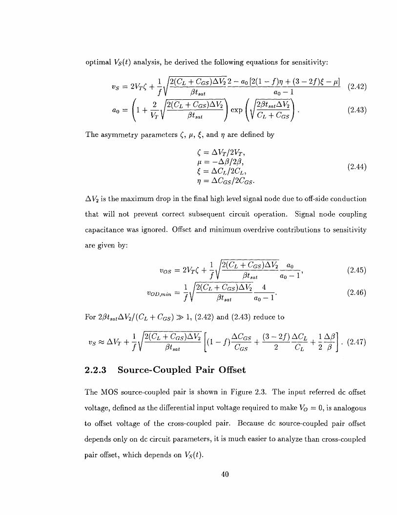
optimal Vs(t) analysis, he derived the following equations for sensitivity:
VS = 2VT(
ao = 1 +
1 2(CL+CS)V22 - ao [ 2 (1 - f +(3 - 2f) - p]
ftsat ao - 1
2 2(CL + CGs)AV2
VT /tsat
( 2/tsatAV2
CL + CGS
The asymmetry parameters (, p, , and i are defined by
( = AVT/2VT,pt = -Afi/2fi,
= ACL/2C L= ACGS/ 2 CGS.
AV2 is the maximum drop in the final high level signal node due to off-side conduction
that will not prevent correct subsequent circuit operation. Signal node coupling
capacitance was ignored. Offset and minimum overdrive contributions to sensitivity
are given by:
voS = 2VT( +1 2(CL + CGS)AV 2 a0
f Ptsat ao - 1
VOD~if 1 I 2(CL + CGS) AV2 4VOD,min = - 3 st a -
f /) sat ao - to
For 2#tsat AV2/(CL + CGS) > 1, (2-42) and (2.43) reduce to
1 2(CL + CGS)AV 2
f Otsat
ACGS-- f) CGS
(3 - 2f) ACL2 CL
2.2.3 Source-Coupled Pair Offset
The MOS source-coupled pair is shown in Figure 2.3. The input referred dc offset
voltage, defined as the differential input voltage required to make Vo = 0, is analogous
to offset voltage of the cross-coupled pair. Because dc source-coupled pair offset
depends only on dc circuit parameters, it is much easier to analyze than cross-coupled
pair offset, which depends on Vs(t).
(2.42)
(2.43)
(2.44)
(2.45)
(2.46)
(2.47)+ .A2 #
RL1
ID1
V )-Hd
RL2
ID2
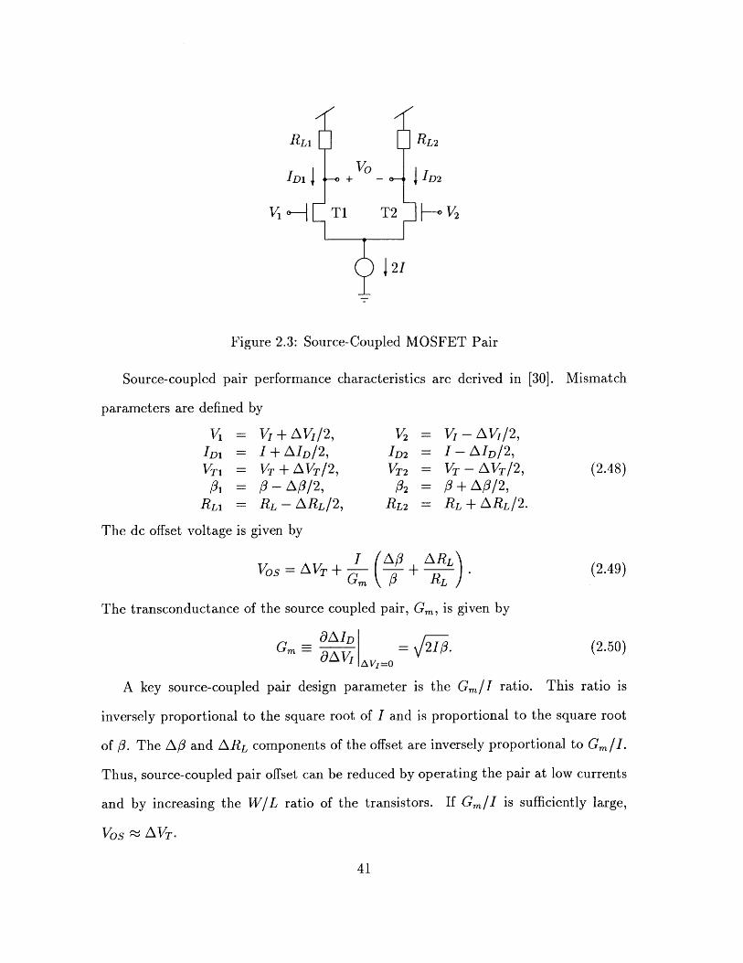
Figure 2.3: Source-Coupled MOSFET Pair
Source-coupled pair performance characteristics are derived in [30].
parameters are defined by
V = V1 i+ AV 1/2,D1 = -+ AID/2,
Vr1 = VT + AVT/2,
#1 = /3-A#/2,L1
V2 = V 1 - AVi/2,ID2 I~- AID/2,VT2 = VT - AV/2,
#2 = + A3/2,RL2 = RL + ARL/2.
The dc offset voltage is given by
(A#/3
ARL+ .
RL
The transconductance of the source coupled pair, Gm, is given by
= 21/3.
A key source-coupled pair design parameter is the Gm/I ratio. This ratio is
inversely proportional to the square root of I and is proportional to the square root
of #. The A# and ARL components of the offset are inversely proportional to Gm/I.
Thus, source-coupled pair offset can be reduced by operating the pair at low currents
and by increasing the WIL ratio of the transistors. If Gm/I is sufficiently large,
Vos ~ AVT.
Mismatch
I
R = RL - ARL/2,
(2.48)
IVos = AVr + G
Gm(2.49)
Gm =AID (2.50)

These results suggest a tradeoff between cross-coupled pair sensing speed and
sensitivity. To increase sensing speed, Vs(t) must decrease more rapidly, resulting in
greater on-side and off-side currents. Higher currents imply a smaller Gm/I ratio.
Thus, increasing sensing speed will likely result in greater offset.
2.2.4 Design Impacts
A speed versus power and sensitivity tradeoff is inherent to the cross-coupled pair. A
faster latch node potential reduction increases sensing speed but also increases off-side
current and reduces sensitivity.
In general, overall performance can be improved by reducing the total signal node
capacitance. Signal node capacitance can be reduced by isolating the signal nodes
from the bitlines during sensing. Equations (2.13) and (2.22) show that for a fixed off-
side current level, reducing CL will increase sensing speed. Equations (2.36), (2.38),
(2.41), and (2.47) suggest that for a fixed sensing speed, reducing CL will improve
sensitivity.
Reducing CL is not always beneficial. Unless CL is large relative to C c and CGS,
performance may be degraded. As CL is reduced, the high signal potential drop
due to coupling increases according to Equation (2.21). If CL and (CC + COGS) are
comparable, the increase may be substantial.
Increasing device widths, W, improves amplifier performance at the expense of
additional circuit area. Increasing W increases #. Equations (2.13) and (2.22) show
that for a fixed off-side current level, increasing # will increase sensing speed. Equa-
tions (2.36), (2.38), (2.41), and (2.47) suggest that for a fixed sensing speed, increasing
# will improve sensitivity. In addition, since for a given process AW is likely inde-
pendent of W, a larger absolute W value should produce a smaller AW/W ratio,
improving sensitivity.
A # and circuit area verses AVT and AL/L tradeoff must be made in selecting
device lengths. Short channels give higher # values and reduce circuit area. However,
short channel devices exhibit a strong threshold voltage dependence on channel length
due to short channel effects. In addition, a larger absolute L value should produce a
smaller AL/L ratio.


Chapter 3
Sense Amplifier Design Evolution
3.1 4K DRAM Generation
The 4K DRAM Generation represents the emergence of modern DRAM design. In
this generation NMOS technology supplanted PMOS technology, the single transis-
tor cell replaced the three-transistor cell, and the divided bitline architecture and
balanced flip-flop sense amplifier were first employed. Mostek introduced address
multiplexing, reducing package size.
3.1.1 Texas Instruments
The 4K DRAM published by TI in 1973 [31] is one of the first commercial DRAMs
to use the divided bitline architecture and balanced flip-flop sense amplifiers. The TI
DRAM, like many other 4K DRAMs, employs a single polysilicon cell with diffused
bitlines and metal wordlines. Three power supplies are required: +12 V for all circuits
except the output buffer, +5 V for the output buffer, and -3 V for substrate biasing.
Though each bitline segment has only 32 cells, the large bitline junction capacitance
results in a sense signal of only 200 mV. The storage capacitance is approximately
100 fF and the cell area is approximately 1300 mm2 .
The TI 4K DRAM sense amplifier is shown in Figure 3.1. During standby the
I

bitline
dummycell
Tdummy
cell
Figure 3.1: TI 4K DRAM Sense Amplifier
load clock, LC, is low and the equalization clock, EQ, is high, shorting the two
bitline segments together. The cross-coupled transistor pair pulls the segments down
to +1 VT above ground. The segments may float below this potential. The dummy
storage capacitors, equal in capacitance to the cell storage capacitors, are precharged
to a potential approximately midway between the stored '0' and '1' voltage levels.
After EQ is pulled down, the selected wordline and dummy wordlines are activated.
Driving LC high turns on the load transistors, activating the flip-flop. Initially both
signal node potentials rise. The difference in signal node potentials causes a difference
in load currents which tends to equalize the potentials. As the signal node potentials
rise above VT, the difference in driver transistor currents increases. Amplification
begins when the difference in driver transistor currents exceeds the difference in load
transistor currents. Eventually, the flip-flop reaches a stable state.
The TI sense amplifier circuit requires only two clock signals, LC and EQ. These
bitline
signals carry current only when charging or discharging sense amplifier device gates.
Employing clock signals to drive the sources of the cross-coupled transistors would
require a substantial increase in chip area to accommodate the clock drivers.
To minimize signal loss due to load current differences, LC should have a short
rise time. As the load device overdrives increase, the ratio of the current difference to
the common-mode current decreases. Thus, less signal is lost as the common-mode
bitline potentials increase.
Because the bitline precharge voltage is not midway between the '0' and '1' poten-
tials, the use of dummy cells is necessary to produce reference potentials on bitline
segments opposite the segments connected to the selected cells. A voltage genera-
tor provides a dummy storage capacitor precharge potential which tracks the supply
voltage and the threshold voltage.
Selection of load transistor dimensions involves a tradeoff between amplifier speed
and power. Load transistor currents are proportional to the W/L ratio of the devices.
Higher current levels produce a faster increase in the high bitline potential. Lower
currents limit dynamic and static power dissipation.
Amplifier sensitivity depends on the ratio of the driver and load transistor gain
factors, #D and /L. The load and driver transistor current differences are proportional
to #L and OD, respectively. Load transistor current differences work to reduce the
signal. Unless #D is several times larger than #L, the common-mode bitline potential
at which the driver transistor current difference begins to exceed the load transistor
current difference will be quite large. As a result, the initial signal will be significantly
reduced before amplification begins.
The final high and low bitline potentials also depend on the #D!/L ratio. A larger
#D//L ratio will give a lower final low bitline potential. As long as the final low
potential is less than +1 VT, the final high potential will approach VDD - VT.

The #D/!L ratio can be increased either by increasing the width of the driver
transistors or decreasing the W/L ratio of the load transistors. Increasing the width
of the driver transistors requires additional layout area. Decreasing the W/L ratio of
the load transistors reduces amplifier speed.
The low bitline precharge potential compromises sensitivity. Load transistor cur-
rents must increase the common-mode bitline potential before amplification begins.
Even if the amplifier is perfectly balanced, load transistor current differences will
reduce the signal. Load transistor mismatches may increase the current difference.
In addition, bitline capacitance variations may increase the difference in the rate
at which the bitline potentials rise. These problems are accentuated if the bitline
potentials float below +1 Vr during precharge.
Because of the low bitline precharge potential, signal development is relatively
fast. In the worst case, signal development begins when the wordlines reach +2 VT.
In addition, the maximum transfer device overdrive is large. Signal development
would be even faster if the bitlines were precharged to ground. However, a larger
increase in the common-mode bitline potential would be required to initiate signal
amplification. Thus, sensitivity would be degraded.
A higher bitline precharge potential would improve sensitivity and reduce the load
current required to increase the high bitline potential. However, if a higher precharge
potential were employed the sources of the cross-coupled transistors could not be tied
directly to ground. In addition, signal development would be slower.
3.1.2 Microsystems International
Foss and Harland published a Microsystems International 4K DRAM design in 1975
[32], [33], paying particular attention to sense amplifier design. Like the TI 4K
DRAM, the Microsystems International DRAM employs a single polysilicon cell with

VDD
LC
bitline ZT - -ZE bitline
SC
Figure 3.2: Microsystems International 4K DRAM Sense Amplifier
diffused bitlines and metal wordlines. +12 V VDD and +5 V Vcc supplies are used.
A 120 fF storage capacitance is achieved with an approximately 1250 pm 2 cell area.
Each bitline segment includes 32 cells, resulting in a 1 pF bitline segment capacitance.
Chip area is about 13 mm2.
The sense amplifier is shown in Figure 3.2. During standby the load clock, LC,
and the set clock, SC, are low. CE is high, precharging the bitlines and the latch
node to Vcc. A read operation begins with CE going low. The selected wordline is
activated. The potentials of bitline segments connected to cells storing a '1' increase.
The potentials of segments connected to cells storing a '0' decrease. Bitline segments
on the side of the sense amplifier opposite the selected wordline remain at Vcc.
Once signal development is complete SC rises, gradually pulling the latch node
towards ground. While the higher signal node potential remains near Vcc, the lower
node potential decreases towards ground. As the lower potential node reaches ground,
LC goes high, slowly pulling the higher potential node to VDD - VT-
The sensitivity and speed of the amplifier depend on the rise time of the set clock.
' !- !. ! - -- - -axaw. -j

A slower rise time reduces susceptibility to circuit mismatches. A faster rise time
improves amplifier speed.
The column access circuits are designed to read the selected column before the
high potential bitline segments are pulled up by the load transistors. As a result, chip
access time is independent of load transistor operation. In addition, because the load
transistors are not active during initial sensing, load transistor mismatches will not
significantly degrade amplifier sensitivity.
A tradeoff must be made between cycle time and power dissipation. A larger load
transistor W/L ratio reduces the time required to restore '1' cell potentials. A smaller
W/L ratio reduces sense amplifier power dissipation.
The sensing scheme does not employ dummy cells. As a result, the bitline
precharge potential determines the '0' and '1' signal magnitudes. Charge injected
from the wordline to the selected bitline segment must be considered when choosing
the precharge potential. The benefits of avoiding dummy cells include reduced chip
complexity and layout area savings.
Use of the Vcc supply voltage for the bitline precharge potential avoids the com-
plexity and layout area of an internal voltage generator and is convenient for signal
margin testing. However, the precharge potential will not track other internal voltages
and circuit parameters. As a result, the signal margin may be reduced.
Separate transistors are used to pull down each latch node. An alternative to
this approach is to connect all the latch nodes together and use a single shared pull
down circuit. If a shared pull down circuit is employed, sense amplifier operation is
sensitive to the total current in the latch node set bus and is therefore sensitive to the
stored data pattern. Use of separate transistors allows better latch node control and
avoids the need for a latch node driver capable of carrying large currents. However,
extra sense amplifier layout area for the latch node pull down and precharge devices
50

is required.
3.2 16K DRAM Generation
Power dissipation considerations played a key role in 16K DRAM design. Typical 4K
DRAMs have only 64 sense amplifiers. In typical 16K DRAMs, 128 sense amplifiers
are active during read cycles. The increase in the number of active sense amplifiers
necessitated substantial reduction in power dissipation per sense amplifier.
Activating static load devices during sensing results in significant off-side current.
Most 16K DRAM designs precharge bitlines to VDD in order to minimize, if not
eliminate, activation of load devices during sensing.
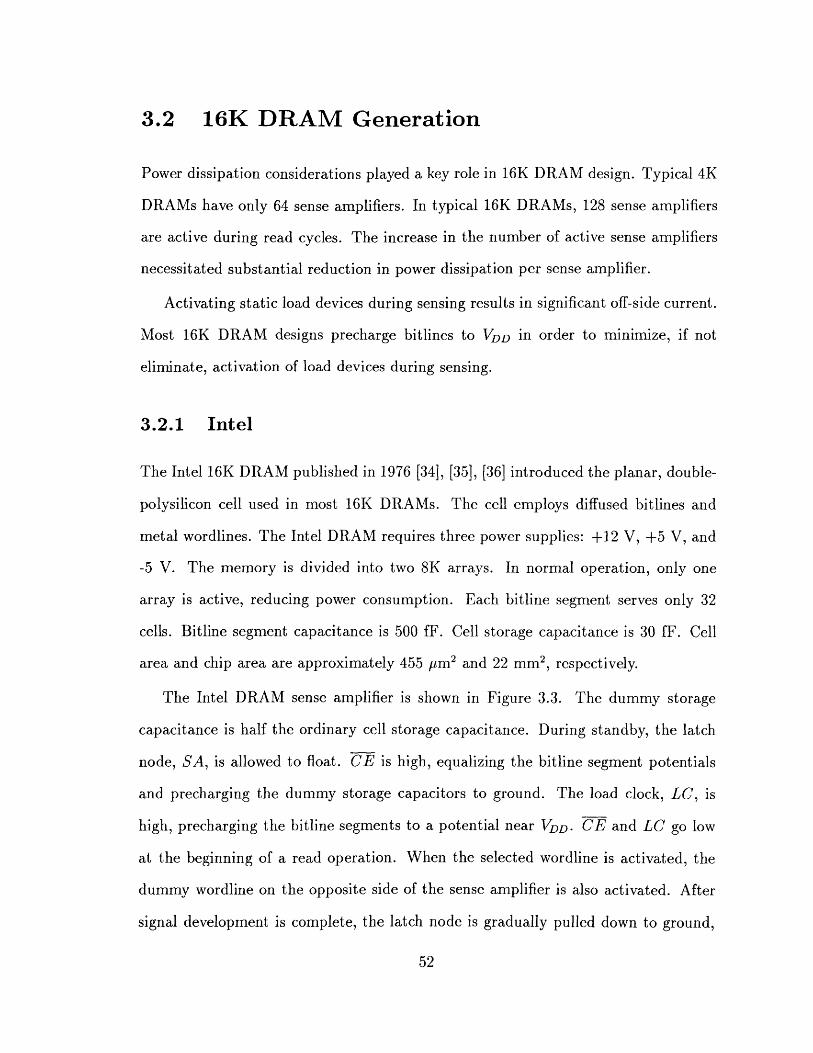
3.2.1 Intel
The Intel 16K DRAM published in 1976 [34], [35], [36] introduced the planar, double-
polysilicon cell used in most 16K DRAMs. The cell employs diffused bitlines and
metal wordlines. The Intel DRAM requires three power supplies: +12 V, +5 V, and
-5 V. The memory is divided into two 8K arrays. In normal operation, only one
array is active, reducing power consumption. Each bitline segment serves only 32
cells. Bitline segment capacitance is 500 fF. Cell storage capacitance is 30 fF. Cell
area and chip area are approximately 455 pm 2 and 22 mm 2 , respectively.
The Intel DRAM sense amplifier is shown in Figure 3.3. The dummy storage
capacitance is half the ordinary cell storage capacitance. During standby, the latch
node, SA, is allowed to float. CE is high, equalizing the bitline segment potentials
and precharging the dummy storage capacitors to ground. The load clock, LC, is
high, precharging the bitline segments to a potential near VDD. CE and LC go low
at the beginning of a read operation. When the selected wordline is activated, the
dummy wordline on the opposite side of the sense amplifier is also activated. After
signal development is complete, the latch node is gradually pulled down to ground,
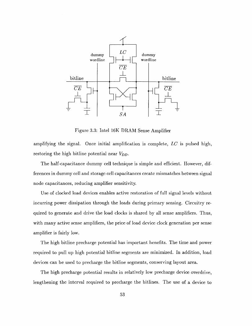
Figure 3.3: Intel 16K DRAM Sense Amplifier
amplifying the signal. Once initial amplification is complete, LC is pulsed high,
restoring the high bitline potential near VDD-
The half-capacitance dummy cell technique is simple and efficient. However, dif-
ferences in dummy cell and storage cell capacitances create mismatches between signal
node capacitances, reducing amplifier sensitivity.
Use of clocked load devices enables active restoration of full signal levels without
incurring power dissipation through the loads during primary sensing. Circuitry re-
quired to generate and drive the load clocks is shared by all sense amplifiers. Thus,
with many active sense amplifiers, the price of load device clock generation per sense
amplifier is fairly low.
The high bitline precharge potential has important benefits. The time and power
required to pull up high potential bitline segments are minimized. In addition, load
devices can be used to precharge the bitline segments, conserving layout area.
The high precharge potential results in relatively low precharge device overdrive,
lengthening the interval required to precharge the bitlines. The use of a device to

short the bitline segments speeds potential equalization, mitigating this disadvantage.
Without an equalization device, incomplete bitline precharge would likely result in
differences between bitline segment potentials, causing significant signal loss.
In the Intel DRAM, each 8K array has a common latch node, SA. As a result,
independent latch node set devices need not be included in each amplifier. This saves
sense amplifier area and permits more complex set clock timing.
The latch node decrease rate depends on the total capacitance seen by the driver.
Until the latch node is pulled +1 VT below a bitline potential, the driver does not
see the bitline capacitance. Suppose one sense amplifier is detecting a '1' and all
other amplifiers are detecting a '0', the average bitline segment potential of the '1'
column will be greater than that of the '0' columns. As SA falls, the '1' column sense
amplifier will be activated before the '0' column sense amplifiers. Until the '0' column
sense amplifiers are activated, the capacitance seen by the driver is relatively low and
SA decreases rapidly. Therefore, initial sensing by the '1' column sense amplifier
occurs with SA decreasing rapidly. This degrades the sensitivity of the amplifier and
increases the high bitline segment potential reduction during sensing.
3.2.2 Mostek
The Mostek 16K DRAM, presented in 1977 [37], [38], [39] became a de facto industry
standard. The DRAM employed the same double-polysilicon cell structure used by
Intel. It required three power supplies: +12 V, +5 V, and -5 V. The memory consists
of a single 16K array with 64 cells per bitline segment. Bitline segment capacitance
is 800 fF. The 435 pm 2 cell provides a 40 fF storage capacitance. Chip area is about
220 mm.
The Mostek DRAM sense amplifier, shown in Figure 3.4, introduced the use of
isolation devices to partially decouple the sense amplifier signal nodes from the bitline
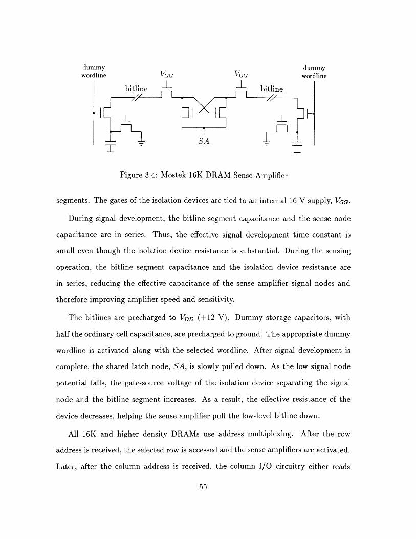
dummy dummywordline VGG VGG wordline
bitline bitline
SA
Figure 3.4: Mostek 16K DRAM Sense Amplifier
segments. The gates of the isolation devices are tied to an internal 16 V supply, VGG-
During signal development, the bitline segment capacitance and the sense node
capacitance are in series. Thus, the effective signal development time constant is
small even though the isolation device resistance is substantial. During the sensing
operation, the bitline segment capacitance and the isolation device resistance are
in series, reducing the effective capacitance of the sense amplifier signal nodes and
therefore improving amplifier speed and sensitivity.
The bitlines are precharged to VDD (+12 V). Dummy storage capacitors, with
half the ordinary cell capacitance, are precharged to ground. The appropriate dummy
wordline is activated along with the selected wordline. After signal development is
complete, the shared latch node, SA, is slowly pulled down. As the low signal node
potential falls, the gate-source voltage of the isolation device separating the signal
node and the bitline segment increases. As a result, the effective resistance of the
device decreases, helping the sense amplifier pull the low-level bitline down.
All 16K and higher density DRAMs use address multiplexing. After the row
address is received, the selected row is accessed and the sense amplifiers are activated.
Later, after the column address is received, the column I/O circuitry either reads
from or writes to the selected sense amplifier. Thus, internally, write cycles amount
to read-modify-write cycles.
In 4K DRAMs and many 16K DRAMs, column I/O circuitry is placed on one
side of the arrays, providing access to only one side of the sense amplifiers. Sense
amplifiers must include load devices in order to write '1' potentials to bitline segments
opposite the column I/O circuitry. Inherent in the use of enhancement load devices
is a speed-power tradeoff.
In the Mostek 16K DRAM, column I/O circuitry is placed between the sense
amplifiers and the storage cell arrays. Access is provided to both sides of the sense
amplifiers. Load devices are not needed to perform writes. The speed-power tradeoff
is avoided, resulting in higher write speed and lower power dissipation [38].
Placement of the column I/O circuitry between the sense amplifiers and the mem-
ory arrays lengthens the bitlines somewhat, increasing bitline capacitance. In addi-
tion, since the column address lines must cross the bitlines, extreme care must be
exercised to avoid destroying the small signals provided by the memory array.
Since load devices are not used during sensing, sense amplifier power dissipation
is very low. However, the latch node potential must be reduced sufficiently slowly to
prevent significant reduction of the high bitline potential.
3.3 64K DRAM Generation
The 64K DRAM Generation manifests many design variations. A key design prob-
lem was maintaining adequate sense signals. 5 V- only DRAMs superseded designs
requiring multiple external power supplies. The elimination of high voltage VDD sup-
plies reduced the difference between stored '1' and '0' potentials. The elimination
of substrate bias supplies necessitated use of on-chip voltage generators to bias the
substrate. Several designs abandoned diffused bitline cells in favor of lower capac-
itance metal bitline cells. Many designs employed folded bitlines. Wordlines were
often bootstrapped to enable storage of a VDD as the '1' potential. Particle-induced
soft errors were a major design problem [20]. Word and column redundancy were
introduced to improve yield [40], [41].
3.3.1 IBM
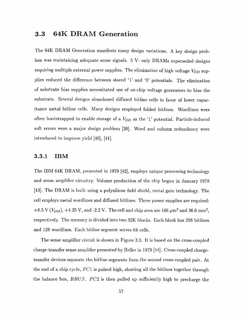
The IBM 64K DRAM, presented in 1979 [42], employs unique processing technology
and sense amplifier circuitry. Volume production of the chip began in January 1978
[43]. The DRAM is built using a polysilicon field shield, metal gate technology. The
cell employs metal wordlines and diffused bitlines. Three power supplies are required:
+8.5 V (VDD), +4.25 V, and -2.2 V. The cell and chip area are 166 [pm 2 and 36.6 mm 2,
respectively. The memory is divided into two 32K blocks. Each block has 256 bitlines
and 128 wordlines. Each bitline segment serves 64 cells.
The sense amplifier circuit is shown in Figure 3.5. It is based on the cross-coupled
charge-transfer sense amplifier presented by Heller in 1979 [44]. Cross-coupled charge-
transfer devices separate the bitline segments from the second cross-coupled pair. At
the end of a chip cycle, PC1 is pulsed high, shorting all the bitlines together through
the balance bus, BBUS. PC2 is then pulled up sufficiently high to precharge the

bitline bitline
--- DPC SA DPC ~:E
VD C TVD Ccc
Figure 3.5: IBM 64K DRAM Sense Amplifier
bitlines to VDD minus the VT of their respective charge-transfer devices. The dummy
storage capacitors are precharged to VDC. The precharge is terminated at the end of
the minimum cycle time. This prevents drops in VDD from trapping the bitlines at a
high potential.
At the beginning of a read cycle, CC and PCI are low. Activation of the wordline
and dummy wordline initiate sense node signal development. CC slowly rises to VDD,
amplifying the signal through the cross-coupled charge-transfer devices. SA is then
pulled down, latching the datum.
The sense amplifier is capable of detecting extremely small signals and is insen-
sitive to most device and capacitance mismatches, including threshold variations.
While other 64K DRAMs required more complex processing technology with lower
CBTICS ratios, the IBM DRAM was produced with a relatively simple process. The
CBT/CS ratio of the IBM DRAM is almost 30.

While much more sensitive than conventional sense amplifiers, the cross-coupled
charge-transfer sense amplifier is also much slower. The rise time of the CC pulse
during initial signal amplification is 85 ns. When precharging the bitlines the bucket
devices operate in a slow source-follower configuration. The IBM 64K DRAM has a
440 ns access time and a 980 ns cycle time.
3.3.2 Texas Instruments
The Texas Instruments 64K DRAM, first published in 1978 [45], [46], used a double-
polysilicon cell structure similar to those commonly used in 16K DRAMs. The chip
operates from a single 5 V power supply. In contrast with most other 5 V- only 64K
DRAMs, the TI DRAM employs a grounded substrate. The memory is organized as a
single block with 256 sense amplifiers and 256 wordlines. Each sense amplifier serves
128 cells. Cell and chip area are approximately 170 pm 2 and 22 mm 2 , respectively.
The TI 64K DRAM sense amplifier circuit is shown in Figure 3.6. Bitlines are
precharged to VDD- When the wordline and dummy wordline are activated, PC2, R1,
and R2 are low. T is high. After signal development is complete, T dips low, partially
isolating the sense nodes from the bitline capacitances. SA is then pulled down to
amplify the signal. T goes high and the low potential bitline is pulled to ground by
the cross-coupled pair. Finally, the high bitline segment is restored to VDD-
The high potential bitline segment is restored to VDD using active loads. First,
R1 goes high, grounding the gate of the restore transistor on the low side of the
sense amplifier and charging the gate of the restore transistor on the high side. R1
then goes low enough to isolate the gates of both restore transistors from the bitline
segments. R2 is pulled up, pushing the gate of the restore transistor on the high side
above VDD and charging the high potential bitline segment to VDD. The wordlines
are bootstrapped above VDD, writing a maximum (VDD) '1' potential.
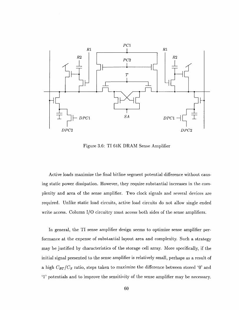
PciR1 IR1
R2 R2PC2
T
SA
DPC2 DPC2
Figure 3.6: TI 64K DRAM Sense Amplifier
Active loads maximize the final bitline segment potential difference without caus-
ing static power dissipation. However, they require substantial increases in the com-
plexity and area of the sense amplifier. Two clock signals and several devices are
required. Unlike static load circuits, active load circuits do not allow single ended
write access. Column I/O circuitry must access both sides of the sense amplifiers.
In general, the TI sense amplifier design seems to optimize sense amplifier per-
formance at the expense of substantial layout area and complexity. Such a strategy
may be justified by characteristics of the storage cell array. More specifically, if the
initial signal presented to the sense amplifier is relatively small, perhaps as a result of
a high CBTICS ratio, steps taken to maximize the difference between stored '0' and
'1, potentials and to improve the sensitivity of the sense amplifier may be necessary.

3.3.3 Fairchild
The Fairchild 64K DRAM, presented in 1980 [47], uses a variation of the folded bitline
array architecture. The memory is divided into four 16K blocks. Each block is divided
into two sections with 64 shared sense amplifiers placed between the sections. Each
section contains 128 wordlines and 128 bitline segments. Thus, each bitline segment
serves only 64 cells.
The Fairchild DRAM employs a double-polysilicon cell with polysilicon wordlines
and metal bitlines. Cell area is 170 pm 2 . Cell storage capacitance is 50 fF. Bitline
segment capacitance is 600 fF. The chip requires a single 5 V power supply. Chip
area is 23.5 mm2
The Fairchild 64K sense amplifier, published by Barnes and Chan in 1980 [48],
is shown in Figure 3.7. Depletion devices are used to isolate bitline segments from
the sense nodes. PC rises to about 7 V to precharge the bitlines to VDD. For
simplicity, assume cells on the selected wordline are connected to one of the top
bitline segments. TO goes low, isolating the bottom bitline segments from the sense
nodes. The wordline and dummy wordline rise to 7 V, allowing complete equalization
of the storage capacitor and bitline segment potentials. After signal development
is complete, TI goes low to temporarily isolate the bitline segments from the sense
nodes. Next, the boost capacitor clock, CC, rises, amplifying the signal and pushing
the sense nodes above VDD- When preamplification is complete, the latch node, SA,
is pulled down, latching the datum. TO and TI rise, allowing the flip-flop to pull the
low level bitline segment to ground.
The shared sense amplifier architecture has several important features. For a given
number of bitline segments, the architecture halves the number of sense amplifiers
required compared with the conventional folded bitline architecture. For a given

DPC DPC
cc
Figure 3.7: Fairchild 64K DRAM Sense Amplifier
number of sense amplifiers, the shared sense amplifier architecture halves the number
of cells per bitline segment, reducing the CBTiCS ratio. The architecture requires the
use of isolation devices. Finally, since column I/O circuitry accesses bitline segments
on only one side of the sense amplifier, all four bitline segments must be active when
reading from or writing to cells on bitline segments opposite the I/O circuitry.
The preamplification scheme insures that the high-level bitline potential will not
fall below VDD. Since the wordlines are bootstrapped to 7 V, full VDD '1' potentials
will be stored. In addition, preamplification allows relatively fast pull-down of the
latching node without significantly degrading amplifier sensitivity. Preamplification
speed, rather than latching speed is critical to sensitivity.
The preamplification circuit requires relatively little layout area. Only two addi-
tional devices per sense amplifier are needed: the two boost capacitors. Active restore
circuits require six devices. The preamplifier circuit requires one clock signal. Active
restore circuits require two.

Use of depletion isolation devices avoids the need for gate potential above the
high level bitline potential. However, the provision of depletion devices in the DRAM
process was undoubtedly warranted by other considerations.

3.4 256K DRAM Generation
By the mid-1980s, features added to improve performance had made NMOS pro-
cesses nearly as complex as CMOS processes. CMOS offers several advantages [49]
over NMOS including lower power dissipation, better clock drivers, and reduced cir-
cuit complexity. Though most 256K DRAMs employ NMOS technology, several use
CMOS.
Almost all 256K DRAMs operate from a single 5 V power supply. Most employ
a Hi-C [50], [51] storage cell. Polycide or silicide wordlines are commonly used to
reduce wordline delay.
3.4.1 Hitachi
The Hitachi 256K NMOS DRAM, published in 1984 [52], [53], typifies the 256K
generation. A Hi-C planar storage capacitor is used with polycide wordlines and
folded metal bitlines. The memory is divided into four 64K blocks. Cell and chip
area are 95 pm 2 and 44.1 mm2, respectively.
The Hitachi 256K DRAM sense amplifier is shown in Figure 3.8. Bitlines are
precharged to VDD. During signal development, the wordline is boosted above VDD
to obtain maximum signal. After signal development is complete, the latch node, SA,
is pulled down, latching the datum. RI goes high, discharging the low-level bitline
segment restore device gate and charging the high-level bitline segment restore device
gate. Next, R1 goes high, pushing the high-level restore device gate above VDD. The
restore device charges the high-level bitline segment to VDD-
A full VDD '1' potential can be stored in NMOS DRAMs either by employing
capacitors to boost the bitline segment potentials or by using active restore circuits.
The Hitachi sense amplifier employs an active restore circuit, avoiding degradation
N

RO R1 CSLDWLO DPC DWL1 VDD SA
I, r -L
Figure 3.8: Hitachi 256K DRAM Sense Amplifier
of the transfer ratio and guaranteeing the restored '1' level will always be VDD, never
higher nor lower.
Aside from the active restore circuits, the Hitachi sense amplifier is quite simple.
Isolation devices are not employed, saving area and eliminating the need for a clock
signal.
3.4.2 Intel
The Intel 256K DRAM, presented in 1984, [54], [55], [56], employs n-well CMOS
technology. p-channel Hi-C cells are placed in an n-well. The n-well isolates the
cells from minority carriers in the substrate, reducing thermal leakage and particle-
induced soft errors. The 70 pm 2 cells, with polysilicon wordlines and folded metal
bitlines, have 55 fF storage capacitors. The memory is divided into eight 32K blocks,
each with 256 wordlines and 128 sense amplifiers. The sense amplifiers, placed in the
middle of the blocks, each serve four bitline segments. Chip area is about 41 mm2 .
The Intel sense amplifier is shown in Figure 3.9. CMOS technology allows active

PC T1 T2 PC
SA
RL RR
Figure 3.9: Intel 256K DRAM Sense Amplifier
bitline restoration using a simple cross-coupled pair. Bitline segments are held at VDD
or ground until the beginning of a cycle. Then the segments are shorted together,
precharging them to 1/2 VDD. TI or T2 goes low to isolate the unselected block
half from the p-channel cross-coupled pair. After signal development is complete,
the cross-coupled pair is isolated from both bitline segment pairs. CC is activated,
boosting the signal node potentials and amplifying the signal. Then the p-channel
latch is set. Finally, the n-channel cross-coupled pairs are activated.
Most 16K and higher density NMOS DRAM sense amplifier designs precharge
bitlines to VDD- Precharging the bitlines to a lower potential reduces the overdrive
on the n-channel latch, decreasing the rate at which the low-level bitline can be pulled
to ground. Restoring a bitline precharged below VDD to VDD requires either static
loads or active restore circuits. Static loads dissipate much power. Active restore
circuits require several sensitive clock signals, use a large amount of area, and may
not have very good current driving capabilities.
Many disadvantages of low bitline precharge potentials do not apply to CMOS
designs. In CMOS DRAMs, '0' and '1' potentials can be restored using a cross-coupled
pair. Restoration can begin before the low-level bitline segment reaches ground.
Intel used half-VDD sensing to eliminate the need for dummy cells and reduce bitline
charging and discharging power. Other benefits of half-VDD sensing are detailed in
[57].
The Intel sense amplifier uses a p-channel cross-coupled pair to latch the datum.
Since the bitlines are precharged to 1/2 VDD, an n-channel cross-coupled pair could
have been used to latch the signal, with p-channel pairs employed to restore the '1'
potentials. Since n-channel devices have greater mobility, using n-channel devices of
equal area as the p-channel devices should reduce the offsets due to process variations.
The advantage of using p-channel devices in the Intel sense amplifier is a reduced soft
error rate. Because the Intel DRAM is fabricated using an n-well process with a p-
channel array, the p-channel cross-coupled device pair can be embedded in the array
n-well. The n-well acts as a barrier to carriers generated in the substrate.
The two bitline segment pairs are serviced by separate n-channel cross-coupled
pairs. Instead, a single n-channel cross-coupled pair could probably be placed in the
center of the blocks, along with the p-channel cross-coupled pair. Use of separate n-
channel pairs allows activation of the restore devices to be staggered, reducing peak
current.

3.5 IM DRAM Generation
The IM DRAM generation represents the midpoint of the transition from NMOS to
CMOS technologies. Almost all CMOS IM DRAMs precharge bitlines to 1/2 VDD. To
reduce wordline delays, IM DRAMs commonly employ polysilicon wordlines strapped
by metal bypass wordlines. Polycide is often used for bitlines. To maintain adequate
charge capacity, Hi-C planar cells are used with 1/2 VDD biased plates.
3.5.1 Toshiba
The Toshiba IM CMOS DRAM, presented in 1985 [58], [59], [60], is typical of 1M
CMOS DRAMs. The 34.2 pm2 planar cell provides a 42 fF storage node. The cell
plate is biased to 1/2 VDD. Polycide bitlines and polysilicon wordlines are employed.
The polysilicon wordlines are connected to metal bypass wordlines at 64-bit intervals.
The folded bitline architecture is used; bitline segments each serve 128 cells. Chip
area is 62.5 mm2 .
The Toshiba sense amplifier is shown in Figure 3.10. At the beginning of the
cycle, a pair of dummy wordlines, DWLO and DWLO or DWL1 and DWL1, are
selected. Upon wordline activation, one of the selected dummy wordlines goes from
Vpc to VDD, the other goes from Vpc to ground. The dummy wordlines couple to
the bitline segments through capacitors with approximately half the capacitance of
the cell storage capacitor. Thus, if Vpc drifts above or below 1/2 VDD the change in
potential caused by activation of the dummy wordlines will compensate, preventing
signal loss. After the cells are restored, EQ goes high, precharging the bitlines. A
voltage generator is tied to Vpc.
In a 1/2 VDD precharge scheme, equalizing the bitlines at the end of the cycle risks
signal loss. If a long time elapses before the beginning of the next cycle terminates

DWLO DWL1 CSLVPc EQ DWLO DWL1 SAP S N
Figure 3.10: Toshiba IM DRAM Sense Amplifier
the precharge period, the bitline potentials may drift from 1/2 VDD- If dummy cells
are not used or if the dummy wordlines are activated through the entire precharge
interval, an offset may be introduced. If the bitline and dummy storage capacitor
potentials move above 1/2 VDD, '1' signals will be reduced. If the potentials move
below 1/2 VDD, '0' signals will be reduced. If the bitlines are held at VDD and ground
until the beginning of the next cycle, access time will suffer.
The complementary capacitor-coupled dummy cell and the bitline precharge volt-
age generator prevent signal loss while allowing bitline precharge to take place at the
end of the cycle. The generator suppresses fluctuations in bitline potentials during
precharge. The complementary capacitor-coupled dummy cell adjusts the reference
bitline segment potential during signal development to compensate for precharge po-
tential variations.
There are important drawbacks to the Toshiba sense amplifier design. The bitline
precharge voltage generator undoubtedly requires significant power and layout area.
Process variations and supply voltage fluctuations may significantly degrade the ac-
curacy of the generator. Traditional dummy cell structures are very much like the
~rn -~
storage cells structures. As a result, cell process variations are often compensated by
similar variations in the dummy cells. The complementary capacitor-coupled dummy
cell structure is quite different from the storage cell structure and therefore may not
offer the same degree of tracking.
3.5.2 Texas Instruments
The Texas Instruments 1M CMOS DRAM, presented in 1986, [61], [62], employs a
unique architecture to accommodate a unique trench cell and reduce the OBLICS
ratio. The memory is divided into four 256K blocks, each with 512 rows and 512
columns. The trench cell employs diffused bitlines and polycide wordlines. Each
column contains eight diffused bitline segments, placed end-to-end. Each segment
connects to 32 cells. Two metal bitlines run parallel to the diffused bitline segments.
A segment select line runs perpendicular to the bitlines at each inside bitline segment
end. When the segment select line is activated, one segment is connected to each
metal bitline.
The trench storage capacitance is 50 fF. Bitline segmentation gives a OBLICS
ratio of only 8. Cell area and chip area are approximately 21 pm 2 and 50 mm2,
respectively.
The Texas Instruments sense amplifier, shown in Figure 3.11, uses full-size dummy
storage capacitors, precharged to VDC. Bitline segments are precharged to 1/2 VDD-
Before the wordline and dummy wordline are pulled up, the isolation device clock,
T, and the appropriate segment select line are activated. After signal development
is complete, T falls, isolating the flip-flop from the bitlines. After the selected sense
amplifier is read from or written to, the isolation device clock, the selected segment
line, and the wordline are bootstrapped above VDD, restoring the cells to full VDD
and ground potentials.
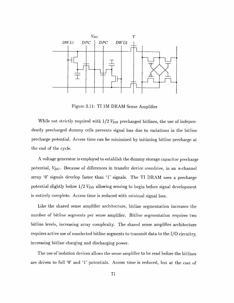
VDC
Figure 3.11: TI IM DRAM Sense Amplifier
While not strictly required with 1/2 VDD precharged bitlines, the use of indepen-
dently precharged dummy cells prevents signal loss due to variations in the bitline
precharge potential. Access time can be minimized by initiating bitline precharge at
the end of the cycle.
A voltage generator is employed to establish the dummy storage capacitor precharge
potential, VDC. Because of differences in transfer device overdrive, in an n-channel
array '0' signals develop faster than '1' signals. The TI DRAM uses a precharge
potential slightly below 1/2 VDD allowing sensing to begin before signal development
is entirely complete. Access time is reduced with minimal signal loss.
Like the shared sense amplifier architecture, bitline segmentation increases the
number of bitline segments per sense amplifier. Bitline segmentation requires two
bitline levels, increasing array complexity. The shared sense amplifier architecture
requires active use of unselected bitline segments to transmit data to the I/O circuitry,
increasing bitline charging and discharging power.
The use of isolation devices allows the sense amplifier to be read before the bitlines
are driven to full '0' and '1' potentials. Access time is reduced, but at the cost of
FF"" Z

additional layout area and circuit complexity.
72

3.6 4M DRAM Generation
To achieve adequate storage cell charge capacity, 4M DRAMs employ either trench or
stacked capacitor cells. Almost all 4M DRAMs use CMOS technologies. Metal bypass
wordlines are commonly employed. Sense amplifier designs are generally similar to
IM CMOS DRAM designs.
3.6.1 Toshiba
The Toshiba 4M DRAM design, presented in 1986 [63], [64], uses a twin-tub CMOS
process. The 17.4 pm 2 trench cells are placed in p-wells on a p-substrate. Cell
storage capacitance is 40 fF. Folded bitlines are formed using polycide. Polysilicon
wordlines are strapped with metal bypass wordlines. Bitline segment capacitance is
600 fF. The memory is divided into sixteen 512K blocks. Chip area is 137 mm 2 . The
DRAM includes an on-chip voltage converter. The chip can be operated either from
the external 5 V supply or from an internal 3.5 V supply controlled by the voltage
converter. A metal mask option is used to change between supply options.
The 4M DRAM sense amplifier is shown in Figure 3.12. Bitlines are precharged to
1/2 VDD at the end of the cycle. Full-capacitance dummy cells are also precharged to
1/2 VDD- Use of dummy cells reduces the sense amplifier susceptibility to variations
in the bitline precharge voltage.
The n-channel flip-flops are activated before the p-channel flip-flops. Isolation
devices, with gates tied to VDD, separate the bitline segments and the n-channel
flip-flops. The isolation devices reduce the effective initial signal node capacitances,
speeding signal amplification. The p-channel cross-coupled pair is connected directly
to the bitlines, allowing full VDD '1' level restoration without bootstrapping the iso-
lation device gates above VDD-

VPC VDC DWL VDC VDD CSLEQ EQL DWL EQL SAP SAN
Figure 3.12: Toshiba 4M DRAM Sense Amplifier
Clocking the isolation device gates would allow further reduction of the effective
signal node capacitance and would allow quick development of a full Vcc signal.
However, the necessary clock timing and driver circuitry would likely increase chip
area and power dissipation.

-~ .- ~ I
3.7 16M DRAM Generation
While 16M DRAMs have not yet been produced in volume, several designs have been
published. All employ CMOS technology and either stacked capacitor or trench cells.
Issues of increased importance in 16M and higher density DRAM designs include
signal development time, bitline to bitline coupling, and sense amplifier layout. New
design approaches have been introduced in response to these issues. Instead of con-
sidering specific 16M DRAM sense amplifier designs, new design approaches which
seem especially relevant to 64M DRAM design will be examined.
3.7.1 Twisted Bitline Architecture
The reduced bitline pitch of 16M and higher density DRAM cells results in high
bitline to bitline capacitance. This capacitance introduces noise during both signal
development and signal amplification.
Figure 3.13 shows a folded bitline model including bitline coupling capacitance.
CBG is the total bitline segment to ground capacitance. CBB is the total capacitance
between neighboring bitlines.
Assuming the states of all odd columns are identical and the states of all even
columns are identical, the bitline segment charges after signal development is complete
are given by
QBLO = AVoddCBB + VBLOCBG + (VBLO - VBLE)CBB,
QBL = - AVoddCBB + VBLOCBG + (VBLO - VBLE)CBB,(3.1)
QBLE - AVevenCBB + VBLECBG + (VBLE - VBLO)CBB,
Q-E = -AVevenCBB + VLECBG + (VL-E - VBLO )CBB ,
where VBLE, VBLE, VBLO, and VBLQ are the bitline segment potentials; AeVen
VBLE - VBLE; and AVodd VBLO - V-LO.
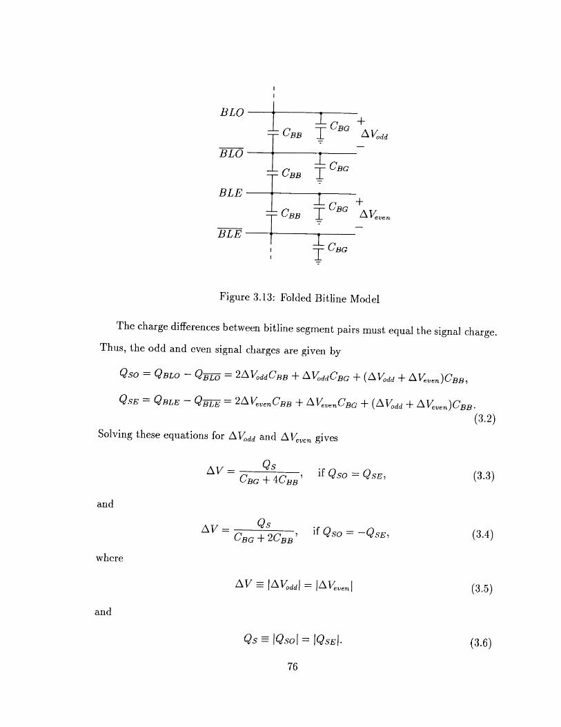
BLO
TCBB CBG
BLO
BLE
BB
BLE
CBG
Figure 3.13: Folded Bitline Model
The charge differences between bitline segment pairs must equal the signal charge.Thus, the odd and even signal charges are given by
QSO = QBLO - Qjj-y = 2 AVoddCBB + AVoddCBG + (AVodd + AVeven)CBB,
QSE = QBLE - QBLE = 2 A evenCBB + A VevenCBG + (A odd + A Veven)CBB -
(3.2)Solving these equations for AVodd and Aeven gives
AV/= QSCBG 4CBB'
AV= - QSCBG +2CBB'
if QSO QSE,
if QSO -QSE,
-Al/Odd
-FAVeve n
and
where
(3.3)
and
(3.4)
AV IAl odd| = Aleven!
QS IQSO| = IQSEI-
(3.5)
(3.6)
C - --
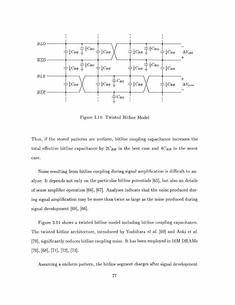
BLO
E CBB [BG CBB ICBB BG CBB A odd
BLO
C B G C B G 1
EE{CBB 1CBB CBB BB
E CBB TCBBT B CBB B +even
BLELCBG
Figure 3.14: Twisted Bitline Model
Thus, if the stored patterns are uniform, bitline coupling capacitance increases the
total effective bitline capacitance by 2 CBB in the best case and 4 CBB in the worst
case.
Noise resulting from bitline coupling during signal amplification is difficult to an-
alyze. It depends not only on the particular bitline potentials [65], but also on details
of sense amplifier operation [66], [67]. Analyses indicate that the noise produced dur-
ing signal amplification may be more than twice as large as the noise produced during
signal development [68], [66].
Figure 3.14 shows a twisted bitline model including bitline coupling capacitance.
The twisted bitline architecture, introduced by Yoshihara et al. [69] and Aoki et al.
[70], significantly reduces bitline coupling noise. It has been employed in 16M DRAMs
[70], [68], [71], [72], [73].
Assuming a uniform pattern, the bitline segment charges after signal development

is complete are given by
QBLO = AVoddCBB + VBLOCBG + (VBLO - VBLE)CBB/ 2 + (VBLO - VBLE)CBB/2,
QBLO = -AVoddCBB + VBLOCBG + (Vi - VBLE)CBB/ 2 + (VBLO - VLE)CBB/ 2 ,
QBLE AVevenCBB + VBLECBG + (VBLE - ViLO)CBBl2 + (VBLE - YBLO)CBB!2,
QBLE = -AVevenCBB + V CBG + (V - VBLo)CBB/2 + (VBLBE B VL)CBB / 2 .
(3.7)
The odd and even signal charges are given by
QsO = QBLO - QBLO = 3 AVodd CBB + LXVoddCBG
(3.8)
QSE = QBLE QBLE = 3 A evenCBB + AVevenCBG
Solving these equations for Ao/dd and AVeven gives
AV = QS _ (3.9)CBG +3CBB
where
AV |Aoddl = |AYevenl (3.10)
and
Qs |QSO= IQSEI- (3.11)
Thus, if the stored patterns are uniform, bitline coupling capacitance increases the
total effective bitline capacitance by 3 CBB, independent of the stored pattern. The
twisted bitline architecture reduces the worst case total effective bitline capacitance
from CBG + 4 CBB to CBG + 3 CBB, compared to the conventional folded bitline ar-
rangement.
The impact of twisted bitlines on coupling noise during signal amplification is
much more significant. In the twisted bitline architecture, inter-pair coupling noise
during signal amplification is canceled. The two bitline segments of each bitline pair
couple equally with neighboring bitline segments.

The twisted bitline architecture requires twice the number of dummy cells and
dummy wordlines as the folded bitline architecture. This not only increases chip
area, but also increases the complexity of the dummy wordline decoder circuitry.
Extra area is also required for the "twists."
The additional area required by the twisted bitline architecture depends on the
technology employed. In the Hitachi 16M DRAM [70], [68], first level metal is used
to twist the silicide bitlines. First level metal is also used to bypass the polysilicon
wordlines. The twists increase total chip area 7 percent. In the Oki [73] and Mitsubishi
[71], [72] DRAMs, special local interconnect levels are used to twist the bitlines,
allowing dummy cells to be placed under twists. In the Oki DRAM, employing
twisted bitlines increases chip area 2.6 percent. In the Mitsubishi DRAM, overhead
is reportedly limited to 0.1 percent.
3.7.2 VT-Derived Bitline Precharge Potentials
Almost all IM and 4M CMOS DRAMs employ a 1/2 VDD bitline precharge potential.
However, in 16M and higher density DRAMs, a 1/2 VDD precharge potential may
result in long signal development time. Two factors contribute to the reduction in
relative signal development speed: delayed initiation of charge transfer due to wordline
rise time and low transfer device overdrive.
In 16M and higher density DRAMs, wordline rise time can be quite large. In
n-channel arrays, '1' cell charge transfer does not begin until the activated wordline
reaches 1/2 VDD + VT. In p-channel arrays, '0, cell charge transfer does not begin until
the activated wordline reaches 1/2 VDD - VT. The delay between wordline selection
and the initiation of charge transfer increases access time.
The reduced internal voltages used in 16M and higher density DRAMs result in
lower transfer device overdrive. Charge transfer speed is limited by transfer device
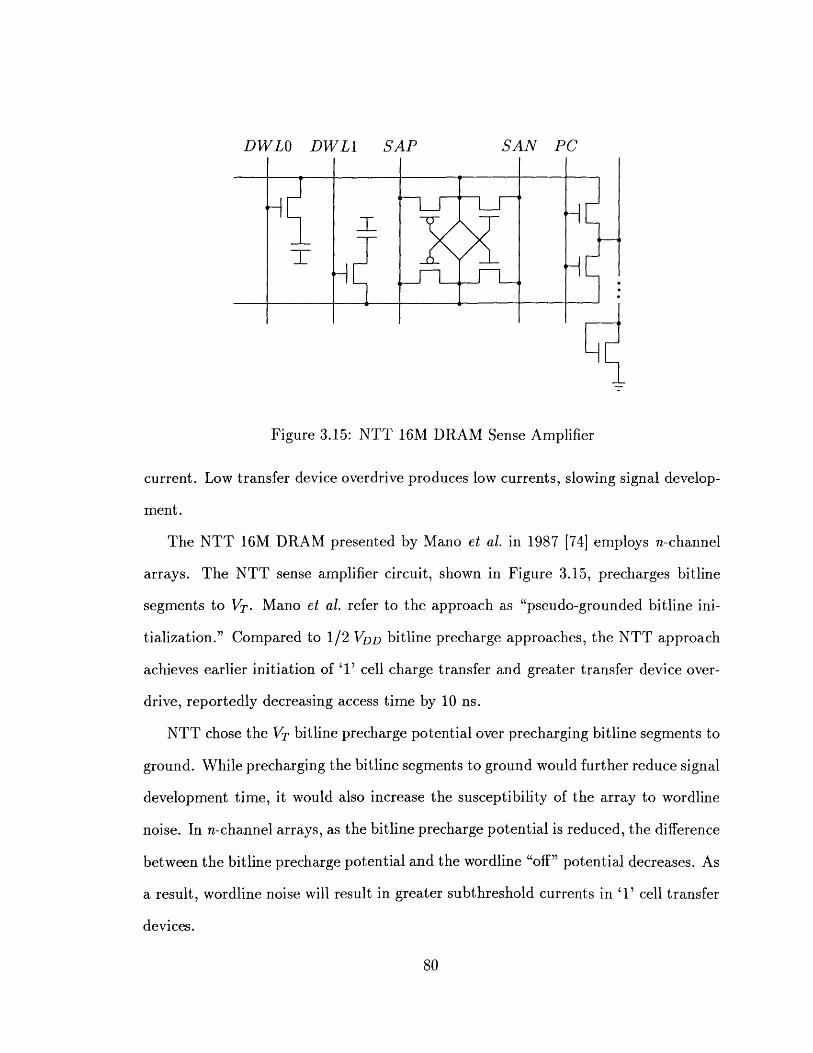
DWLO DWL1 SAP SAN PC
Figure 3.15: NTT 16M DRAM Sense Amplifier
current. Low transfer device overdrive produces low currents, slowing signal develop-
ment.
The NTT 16M DRAM presented by Mano et al. in 1987 [74] employs n-channel
arrays. The NTT sense amplifier circuit, shown in Figure 3.15, precharges bitline
segments to VT. Mano et al. refer to the approach as "pseudo-grounded bitline ini-
tialization." Compared to 1/2 VDD bitline precharge approaches, the NTT approach
achieves earlier initiation of '1' cell charge transfer and greater transfer device over-
drive, reportedly decreasing access time by 10 ns.
NTT chose the VT bitline precharge potential over precharging bitline segments to
ground. While precharging the bitline segments to ground would further reduce signal
development time, it would also increase the susceptibility of the array to wordline
noise. In n-channel arrays, as the bitline precharge potential is reduced, the difference
between the bitline precharge potential and the wordline "off" potential decreases. As
a result, wordline noise will result in greater subthreshold currents in '1' cell transfer
devices.
80

CSL
SANIVDD
Figure 3.16: 2/3 VDD Sense Amplifier Circuit (from [75])
In 1988 Dhong et al. employed the same basic approach as Mano et al. in sense
amplifiers designed for use with a p-channel array [75]. One of the circuits is shown in
Figure 3.16. Bitline segments are precharged to VDD - VT. Since VDD - VT r.2/3 VDD,
Dhong et al. refer to the approach as "2/3 VDD-Sensing."
The important difference between the circuits presented by Mano et al. and Dhong
et al. is the method used to precharge the bitlines. In the Mano et al. design, a
single diode-connected transistor must discharge all the bitlines to the precharge
potential. In the Dhong et al. design, the precharge potential in each column is
produced independently by transistors operating in a source-follower configuration.
In both circuits, the precise precharge potential will likely vary depending on the
length of the precharge interval and the parameters of the precharge transistors. In
the Dhong et al. design, local variations in precharge transistor characteristics may
result in bitline precharge potential variations between different columns. This would
cause signal amplification to begin at different times, increasing bitline coupling noise
during sensing.
t!!n T '! -aw -
3.7.3 Sense Amplifier Pitch Doubling
With each new DRAM generation, cell dimensions have been reduced relative to
feature sizes. As a result, sense amplifier pitch constraints have become increasingly
tight. Using folded bitlines, the sense amplifier pitch constraint can be relaxed to
four bitline pitches by placing sense amplifiers on both sides of each array. Several
16M DRAMs employ this technique [74], [71], [72], [76], [77].
This approach is likely to increase total sense amplifier area. Twice as many sense
amplifier signal and/or supply buses are needed. In addition, particular care must
be taken to prevent timing skews between sense amplifiers on opposite sides of each
array.
82
Chapter 4
64M DRAM Technology andPerformance Projections
Key technology features and performance specifications must be projected to facilitate
64M DRAM sense amplifier analysis. Estimates will be based primarily on published
16M DRAM parameters and historical trends.
16M DRAM chip areas generally range from 130 mm2 to 160 mm2 . Typical cell
areas range from 4 p1m 2 to 5 pm2 . Based on the trends shown in Figures 1.8 and 1.9,
64M DRAM chip and cell areas should be around 200 mm 2 and 2 pm 2 , respectively.
While Tasch and Parker [78] predict significantly smaller 64M DRAM chip and cell
areas, the 200 mm2 and 2 [m 2 estimates are consistent with trend data published by
Maes et al. [27], Lu [26], and Noble [25].
Folded bitline cells will likely be employed in most 64M DRAMs. Almost all
published 1M and higher density DRAMs use folded bitlines. In addition, most
published cells suitable for 64M DRAMs have folded bitlines.
The area of a folded bitline cell is equal to twice the product of the bitline segment
and wordline pitches. Thus, to build a 2 pm 2 cell, the product of the pitches must
be 1 pm2 . Since minimum wordline and bitline pitches are nearly equal, both pitches
will probably be approximately 1 pm.
Minimum 16M DRAM n-channel device lengths range from about 0.5 pm to
0.7 pm. Minimum p-channel device lengths are usually about 0.2 pm greater. Gate
insulator thickness generally falls within the 120 A to 160 A range. Based on the trend
shown in Figure 1.10, 64M DRAM features should be roughly 1.4x smaller than 16M
DRAM features. Thus, minimum 64M n-channel and p-channel device lengths will
likely be about 0.4 pm and 0.5 pm, respectively. Gate insulator thickness will likely
be around 100 A.
Electric fields within devices must be limited to avoid hot electron effects, drain
breakdown, and oxide breakdown [79], [80], [81], [82]. 16M DRAMs typically use
a 5 V external supply, but operate most internal circuits with only 3-4 V. This
preserves compatibility with standard 5 V components while limiting internal fields.
At the 64M integration level, power dissipation considerations dictate a lower external
power supply voltage. The JEDEC supply voltage standard for 64M DRAMs is 3.3 V
[83]. This voltage will likely be used both for external supplies and internal circuits
in most 64M DRAMs.
Subthreshold conduction limits reduction of device threshold voltages [82]. As the
gate-source voltage of a device is decreased below the threshold voltage, device current
does not cease. Instead, the current exponentially decreases. The gate voltage swing
required to reduce the current by one decade is typically on the order of 100 mV. If
device thresholds are too low, substantial current will flow through "off" devices, re-
sulting in significant static power dissipation in peripheral circuits and charge leakage
through the transfer devices in the array. Thus, 64M DRAM devices will probably
not have significantly reduced threshold voltages. Typical nominal device thresholds
may be approximately 0.7 V.
As DRAM cell areas are reduced, bitline to bitline coupling capacitance gener-
ally increases relative to total bitline capacitance [84], [85]. Figure 4.1 shows bitline
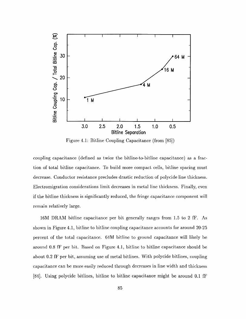
S 'i I i I i 1
30 64 M
-- , 20
8- 4M
10 - M00
m 1 ii i I i
3.0 2.5 2.0 1.5 1.0 0.5Bitline Separation
Figure 4.1: Bitline Coupling Capacitance (from [85])
coupling capacitance (defined as twice the bitline-to-bitline capacitance) as a frac-
tion of total bitline capacitance. To build more compact cells, bitline spacing must
decrease. Conductor resistance precludes drastic reduction of polycide line thickness.
Electromigration considerations limit decreases in metal line thickness. Finally, even
if the bitline thickness is significantly reduced, the fringe capacitance component will
remain relatively large.
16M DRAM bitline capacitance per bit generally ranges from 1.5 to 2 fF. As
shown in Figure 4.1, bitline to bitline coupling capacitance accounts for around 20-25
percent of the total capacitance. 64M bitline to ground capacitance will likely be
around 0.8 fF per bit. Based on Figure 4.1, bitline to bitline capacitance should be
about 0.2 fF per bit, assuming use of metal bitlines. With polycide bitlines, coupling
capacitance can be more easily reduced through decreases in line width and thickness
[84]. Using polycide bitlines, bitline to bitline capacitance might be around 0.1 fF
per bit.
DRAM chip power dissipation has increased only slightly with increases in chip
capacity. The active power dissipated by 16M DRAMs ranges from 300 mW to
600 mW. This range is about 100 mW higher than the 4M range and 200 mW higher
than the IM range. In 16M DRAMs, bitline charging and discharging is the largest
single component of chip power dissipation. Even at a slow 1 ps cycle, bitline current
can be almost one-third of the total chip current [86]. Bitline power requirements will
be even more significant in 64M DRAMs. Thus, typical 64M power dissipation may
be 700 mW or more.
16M DRAM access times generally range from 55 ns to 65 ns. As shown in
Figure 1.6, access times are gradually decreasing. 64M access should be around
50 ns. Typical cycle times should be about 100 ns.
As DRAM chip capacity has increased beyond 256K, the number of refresh cycles
required per unit time has remained constant. Both the refresh interval and the
number of refresh cycles have doubled with each new generation. Almost all 16M
DRAMs require 2048 refresh cycles every 32 ms. 64M DRAMs will almost certainly
require 4096 refresh cycles every 64 ms.
Projected 64M technology and performance parameters are summarized in Ta-
bles 4.1 and 4.2. Design rules were derived from typical lambda-based rules. Di-
mensions were scaled to accommodate projected 64M cell dimensions. The rules are
presented in Table 4.3. While individual rules may differ from actual 64M technology
dimensions, the set as a whole provides valuable insight into layout constraints.

Chip Area 220 mm 2
Cell Area 2 ptm 2
Bitline Pitch 1 Pmn-channel Device Length 0.4 pmp-channel Device Length 0.5 PmGate Insulator Thickness 100 APower Supply 3.3 VDevice Thresholds 0.7 VBitline-to-Ground Capacitance 0.8 fF per bitBitline-to-Bitline Capacitance 0.2 fF per bit
(metal bitlines)
Bitline-to-Bitline Capacitance 0.1 fF per bit(polycide bitlines)
Table 4.1: Projected 64M DRAM Technology Parameters
Power Dissipation 700+ mWAccess Time 50 nsCycle Time 100 nsRefresh Interval 64 msRefresh Cycles 4096
Table 4.2: Projected 64M DRAM Performance Parameters

Gate Poly (GP) Rules:GP width over ND (Nch device length) 0.40 pmGP width over PD (Pch device length) 0.50 pmGP width not over xD ................ 0.40 pmGP spacing ........................... 0.40 pmGP overlap past xD .................. 0.40 pmGP to xD spacing .................... 0.20 pm
1st Level Metal (M1) Rules:M 1 width ............................ 0.50 pimM 1 spacing ........................... 0.50 pm
2nd Level Metal (M2) Rules:M 2 width ............................ 0.80 pmM 2 spacing ........................... 0.80 pm
N and P Diffusion (ND and PD) Rules:xD width ............................. 0.50 pmxD spacing .......--................. 0.50 pmxD width over GP (device width) ..... 0.50 pmxD overlap past GP (S/D length) ..... 0.50 pmND to PD spacing .................... 1.60 pm
Contact (CT) Rules:CT length and width ................. 0.40 pmCT spacing ........................... 0.40 pmCT within xD ........................ 0.20 pmCT within GP ........................ 0.20 pmCT within M 1 ........................ 0.05 pmCT to xD spacing .................... 0.40 pmCT to GP spacing .................... 0.40 pm
M1 - M2 Via (MV) Rules:MV length and width ................. 0.80 pmMV within M 1 ---.................... 0.40 pmMV within M2 ---.................... 0.40 pm
n-well (NW) Rules:NW width ............................ 2.00 pmNW spacing .......................... 1.80 pmND to NW spacing ................... 1.00 pmND within NW ....................... 0.60 pmPD to NW spacing ................... 0.60 pmPD within NW ....--................ 1.00 pm
Table 4.3: 64M DRAM Design Rules
88
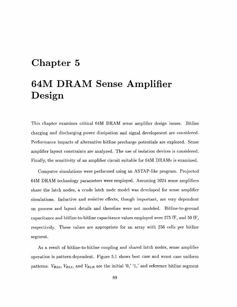
Chapter 5
64M DRAM Sense Amplifier
Design
This chapter examines critical 64M DRAM sense amplifier design issues. Bitline
charging and discharging power dissipation and signal development are considered.
Performance impacts of alternative bitline precharge potentials are explored. Sense
amplifier layout constraints are analyzed. The use of isolation devices is considered.
Finally, the sensitivity of an amplifier circuit suitable for 64M DRAMs is examined.
Computer simulations were performed using an ASTAP-like program. Projected
64M DRAM technology parameters were employed. Assuming 1024 sense amplifiers
share the latch nodes, a crude latch node model was developed for sense amplifier
simulations. Inductive and resistive effects, though important, are very dependent
on process and layout details and therefore were not modeled. Bitline-to-ground
capacitance and bitline-to-bitline capacitance values employed were 275 fF, and 50 fF,
respectively. These values are appropriate for an array with 256 cells per bitline
segment.
As a result of bitline-to-bitline coupling and shared latch nodes, sense amplifier
operation is pattern-dependent. Figure 5.1 shows best case and worst case uniform
patterns. VBLO, VBL1, and VBLR are the initial '0,, '1,' and reference bitline segment

potentials. The '0' and '1' signals, (VBLR - VBLO) and (VBL1 - VBLR), are equal in
magnitude. In the best case pattern, '0' and '1' signals are presented to alternate
sense amplifiers. During sensing, the potentials of adjacent bitline segments con-
nected to different sense amplifiers move in the same directions. Thus, Inter-bitline
coupling has minimal effect on sensing. In the worst case patterns, identical sig-
nals are presented to all sense amplifiers. During sensing, the potentials of adjacent
bitline segments connected to different sense amplifiers move in opposite directions.
Inter-bitline coupling has maximal effect. Except where otherwise noted, worst case
uniform patterns were employed in all sense amplifier simulations.
5.1 Bitline Power Considerations
Sense amplifier power dissipation consists of two components: power intrinsic to
bitline charging and discharging and power due to amplifier inefficiencies. Power
dissipation per bitline pair due to bitline charging and discharging will be calculated
by summing the amount of charge taken from the VDD supply. The analysis will
assume stored '0' and '1' potentials are ground and VDD, respectively.
During signal amplification and cell restoration, one bitline segment must be
charged to the stored '1' potential, VDD. The charge needed from the supply is
Qamp = (VDD - VPc)CBL, (5.1)
where CBL is the bitline segment capacitance. To precharge the bitlines for the next
cycle, the bitline potentials can be first equalized, then charged or discharged to the
precharge potential. The charge needed from the supply is
f 2(Vpc - VDD! 2 )CBL, if VPc > VDD/2 (5.2)Th1 if V VDD/ 2 .p(5iv)
The total amount of charge needed per cycle is given by
QBL ~ Qamp + Qpc = (VDDI 2 +\ Vpc - VDD/ 2 1) CBL. (5.3)
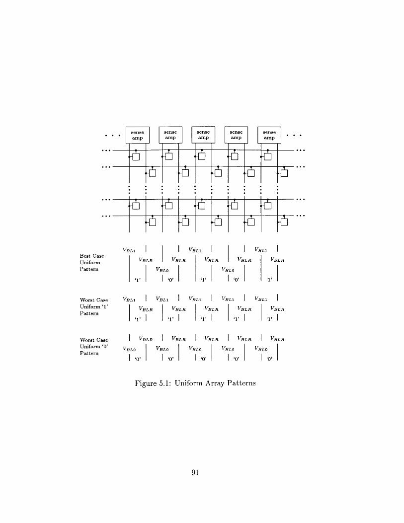
sense sense sense sense senseamp amp amp amp amp
VBL1 IBL1 VBL1Best CaseUniform VBLR VBLR VBLR VBLR VBLR
Pattern VBLO VBLO
'1' ' '1' ' '1'
Worst Case VBL1 VBLI VBL1 BL1 VBL1Uniform '1' VBLR VBLR VBLR VBLR VBLRPattern
'1' I '1' I '1' I'1' I'1' I
Worst Case VBLR VBLR VBLR VBLR VBLR
Uniform'0' VBLO VBLO VBLO VBLO VBLOPattern 0 1 I 1 0
Figure 5.1: Uniform Array Patterns
Active Segment AverageBitline Precharge Cells per Pairs per Bitline Power
Voltage (V) Bitline Segment Sense Amplifier Dissipation (mW)
256 1 550
VDD 512 1 1150128 2 550256 2 1100256 1 360
1/3 VDD or 2/3 VDD 512 1 730128 2 360256 2 730256 1 270
1/2 VDD 512 1 550128 2 270256 2 550
Table 5.1: 64M DRAM Intrinsic Bitline Power Dissipation
Thus, the average power dissipation per bitline pair due to bitline charging and dis-
charging is given by
VDDQBL _ VDD (VDD/ 2 + VPC - VDD/21) CBL (54)PBL,ave .54
tcycle tcycle
To achieve a 4096 cycle refresh, 64M/4096 = 16K cells must be restored each re-
fresh cycle. Consequently, 16K sense amplifiers must be active. Using Equation (5.4),
average intrinsic bitline charging and discharging power dissipation during a 1OOns
refresh cycle was calculated for several memory configurations. The results are shown
in Table 5.1.
Clearly, 64M DRAM intrinsic bitline charging and discharging power dissipation
will be extremely important. In 4M and earlier DRAM generations, intrinsic bitline
power dissipation was not nearly as significant. The growing importance of bitline
power dissipation is due primarily to the increased number of active sense amplifiers
in higher capacity DRAMs.
In general, the typical number of cells per sense amplifier has increased with each
new DRAM generation. Most 16M DRAMs have 512 cells per sense amplifier. From
Table 5.1 it is obvious that increasing the number of cells per sense amplifier to 1024
would result in much higher power dissipation.
Limiting the number of cells per sense amplifier to 512 will require finer segmenta-
tion of 64M DRAMs, increasing chip area and complexity. However, the advantages,
reduced bitline power dissipation and lower transfer ratios, seem likely to outweigh
the costs.
Table 5.1 illustrates a traditional argument for a 1/2 VDD bitline precharge poten-
tial. Intrinsic bitline power dissipation is proportional to jVpc - VDD/21. Thus, in
a 1/2 VDD bitline precharge potential scheme, intrinsic bitline power dissipation will
be half the intrinsic power dissipation in a VDD bitline precharge scheme. However,
intrinsic bitline charging and discharging power dissipation is only one component of
total power dissipation. Other power requirements must also be considered.
5.2 Signal Development Considerations
The time required for signal development depends primarily on cell capacitance and
transfer device current. As DRAM chip capacity increases, cell capacitance remains
relatively stable. Device dimensions and supply voltages are reduced. In saturation,
device current is proportional to (W/L), is inversely proportional to gate oxide thick-
ness, and is proportional to the square of the overdrive voltage. Thus, if device width,
length, and oxide thickness and the overdrive voltage are all scaled by the same factor,
saturation current will decrease as DRAM chip capacity increases. In linear opera-
tion, device current is directly proportional to the overdrive voltage. Thus, if the
threshold voltage and the supply voltage were scaled with device dimensions, device
current in linear operation would remain fairly constant. However, in high density
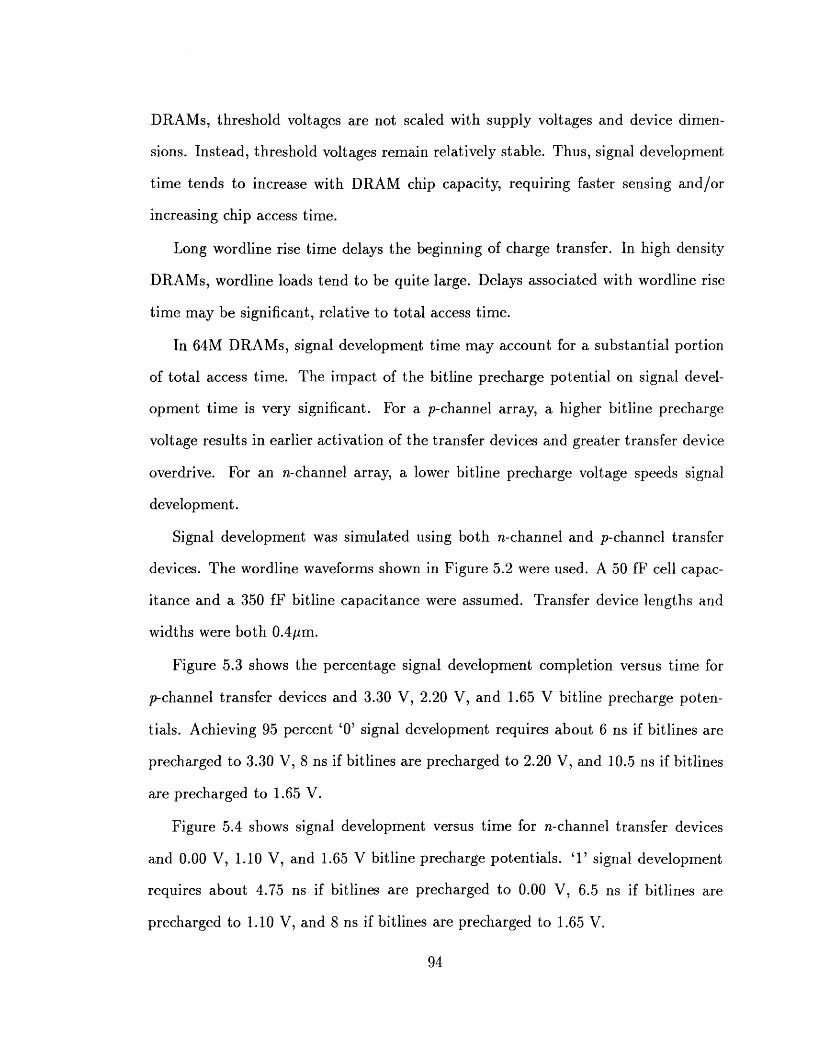
DRAMs, threshold voltages are not scaled with supply voltages and device dimen-
sions. Instead, threshold voltages remain relatively stable. Thus, signal development
time tends to increase with DRAM chip capacity, requiring faster sensing and/or
increasing chip access time.
Long wordline rise time delays the beginning of charge transfer. In high density
DRAMs, wordline loads tend to be quite large. Delays associated with wordline rise
time may be significant, relative to total access time.
In 64M DRAMs, signal development time may account for a substantial portion
of total access time. The impact of the bitline precharge potential on signal devel-
opment time is very significant. For a p-channel array, a higher bitline precharge
voltage results in earlier activation of the transfer devices and greater transfer device
overdrive. For an n-channel array, a lower bitline precharge voltage speeds signal
development.
Signal development was simulated using both n-channel and p-channel transfer
devices. The wordline waveforms shown in Figure 5.2 were used. A 50 fF cell capac-
itance and a 350 fF bitline capacitance were assumed. Transfer device lengths and
widths were both 0.4pim.
Figure 5.3 shows the percentage signal development completion versus time for
p-channel transfer devices and 3.30 V, 2.20 V, and 1.65 V bitline precharge poten-
tials. Achieving 95 percent '0' signal development requires about 6 ns if bitlines are
precharged to 3.30 V, 8 ns if bitlines are precharged to 2.20 V, and 10.5 ns if bitlines
are precharged to 1.65 V.
Figure 5.4 shows signal development versus time for n-channel transfer devices
and 0.00 V, 1.10 V, and 1.65 V bitline precharge potentials. '1' signal development
requires about 4.75 ns if bitlines are precharged to 0.00 V, 6.5 ns if bitlines are
precharged to 1.10 V, and 8 ns if bitlines are precharged to 1.65 V.
94
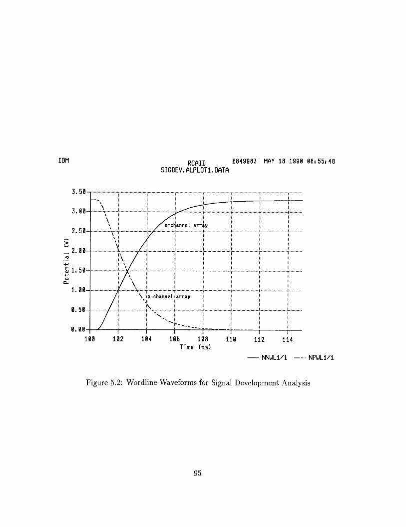
B849983 MAY 18 1990 08: 55: 48RCAIDSIGDEV.ALPLOTi.DATA
100 102 104 10b 108 110 112 114Time (ns)
- NNWLi/1 NPWL1/1
Figure 5.2: Wordline Waveforms for Signal Development Analysis
3. 50
3.
2.
2.
S1.a.
1.
IBM
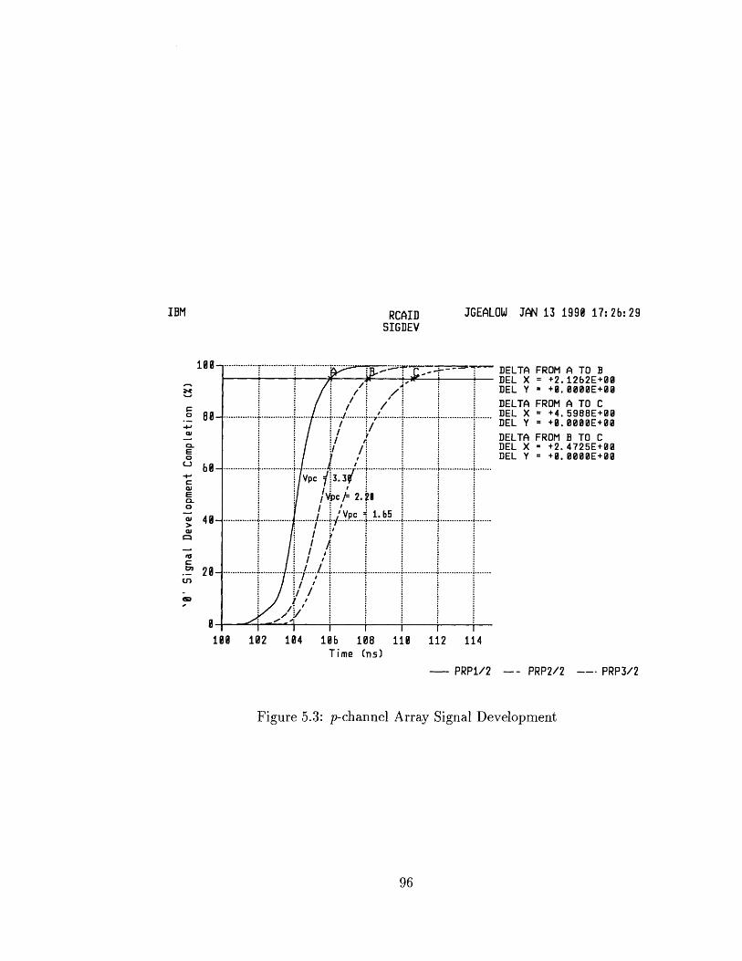
IBM RCAIDJSIGDEV
10
JGEALOW JAN 13 1990 17:2b:29
DELTA FROM A TO BDEL X = +2.i262E+00DEL Y = +0.0000E+00
DELTADEL XDEL Y
FROM A TO C= +4.5988E+00= +8.0000E+00
DELTA FROM B TO CDEL X - +2.4725E+00DEL Y = +0.0000E+00
100 102 104 10b 108 110 112 114Time (ns)
- PRP1/2 -- PRP2/2 --- PRP3/2
Figure 5.3: p-channel Array Signal Development

IBM RCAIDSIGDEV
JGEALOW JAN 13 1990 17:23:35
100 102 104 10b 108Time (ns)
111 112 114
- PRN1/1
DELTA FROM A TO BDEL X = +1.7379E+00DEL Y = +3.0000E+00DELTA FROM A TO CDEL X = +3.24i1E+00DEL Y = +8.0000E+00DELTA FROM B TO CDEL X - +1.5031E+00DEL Y = +1.0000E+00
-- PRN2/1 --- PRN3/1
Figure 5.4: n-channel Array Signal Development
.- go -,. - A
Unless signal development and sensing are both completed within about 20 ns, a
50 ns total access time may not be attainable. If signal development takes longer,
sensing must be completed faster. If a p-channel array is employed, sensing should
require less than 14 ns if bitlines are precharged to 3.30 V, less than 12 ns if bitlines
are precharged to 2.20 V, and less than 9.5 ns if bitlines are precharged to 1.65 V. If
an n-channel array is employed, sensing should require less than 15.25 ns if bitlines
are precharged to 3.30 V, less than 14.5 ns if bitlines are precharged to 2.20 V, and
less than 12 ns if bitlines are precharged to 1.65 V.
These results quantify an important advantage of precharging bitline segments to
higher potentials in p-channel arrays and lower potentials in n-channel arrays. Signal
development time is significantly reduced, relaxing sensing speed requirements.
5.3 Bitline Precharge Potential
Three sense amplifier circuits will be considered. All are designed for use with a
p-channel array. Corresponding circuits can be used with n-channel arrays.
The primary difference between the three sense amplifiers is the bitline precharge
voltage. The purpose of this section is to identify the precharge potential most suitable
for 64M DRAMs. Later, other circuit modifications will be considered.
5.3.1 VDD Sense Amplifier
A sense amplifier designed for use with a full VDD bitline precharge potential is shown
in Figure 5.5. The latch node, SAN, is shared by many sense amplifiers. It is driven
by large n-channel set devices during sensing. Initial sensing is performed entirely
by the n-channel cross-coupled pair. Both p-channel devices remain off until the low
bitline segment potential drops below VDD - VT- As long as the high bitline segment
potential remains above VDD - VT, no current will flow from VDD to the low potential
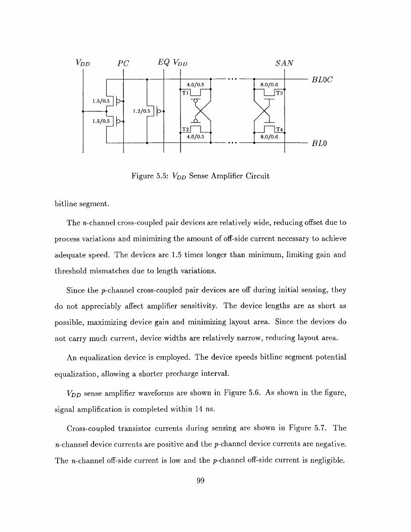
VDD PC EQ VDD SAN
4.6/0.5 8.0/0.6 BLOCTi *_ T3'
1.5/0.5
1.2/0.5
1.5/0.5
T2 T4
4.6/0.5 8.0/0.6-- ' BLO
Figure 5.5: VDD Sense Amplifier Circuit
bitline segment.
The n-channel cross-coupled pair devices are relatively wide, reducing offset due to
process variations and minimizing the amount of off-side current necessary to achieve
adequate speed. The devices are 1.5 times longer than minimum, limiting gain and
threshold mismatches due to length variations.
Since the p-channel cross-coupled pair devices are off during initial sensing, they
do not appreciably affect amplifier sensitivity. The device lengths are as short as
possible, maximizing device gain and minimizing layout area. Since the devices do
not carry much current, device widths are relatively narrow, reducing layout area.
An equalization device is employed. The device speeds bitline segment potential
equalization, allowing a shorter precharge interval.
VDD sense amplifier waveforms are shown in Figure 5.6. As shown in the figure,
signal amplification is completed within 14 ns.
Cross-coupled transistor currents during sensing are shown in Figure 5.7. The
n-channel device currents are positive and the p-channel device currents are negative.
The n-channel off-side current is low and the p-channel off-side current is negligible.

IBM RCAID B849983 MAY 18 1990 10:12:12SAMPi.ALPLOT7.DATA
3.50-
3.800-
2.580-
2.00-
1.50
1.88-
8.58-
L-
s \D
oe BL C
8 2 4 6 8 18 12 14Time (ns)
ANSAN/1 -- NSAP/1 --- NBL8/1 -- NBL8C/1
Figure 5.6: VDD Sense Amplifier Waveforms. 2OmV initial signal. Perfectly balancedamplifier. CBG = 275 fF. CBB = 50 fF.
100
'W

IBM RCAID B849983 MAY 18 1990 09:28:20SAMPI.ALPLOT7.DATA
~ 0 T3
T4
20-
000-1JT-
20-
T2
-040
0 2 4 b a 12 -- JDS.T4.SAMPO/1Time (ns)
- JDS.T1.SAMPO/1 --- JDS.T2.SAMP/1- JDS.T3.SAMPO/i
Figure 5.7: VDD Sense Amplifier Device Currents. 20mV initial signal. Perfectly
balanced amplifier. CRG = 275 fF. CB = 50 fF.
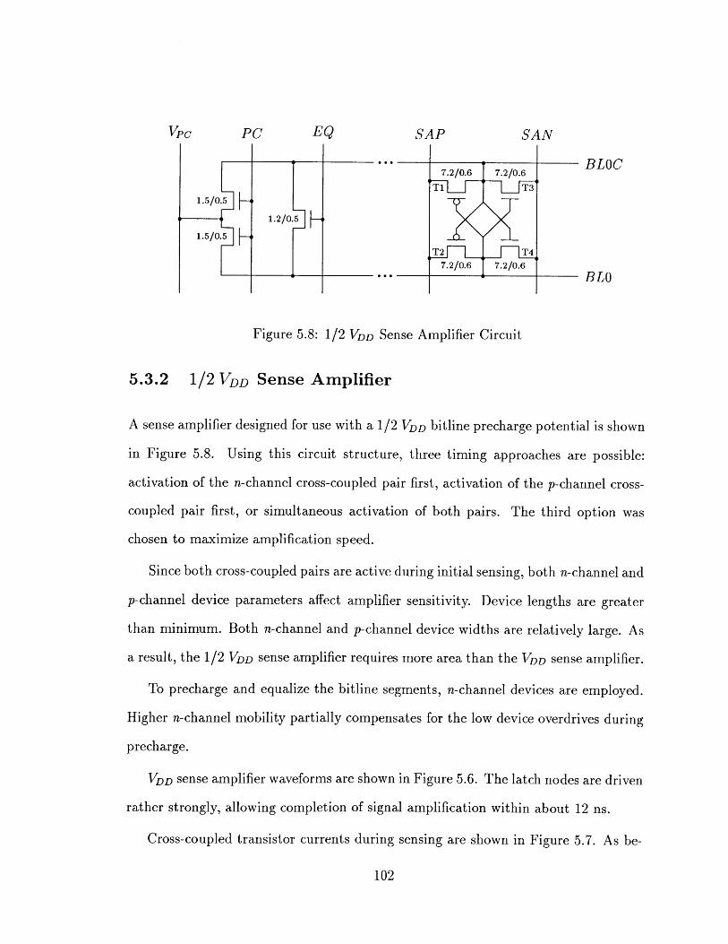
VPC PC EQ SAP SAN
7.2/0.6 7.2/0.6 BLOCT1 T3
1.5/0.5
1.2/0.5
1.5/0.5
T2 T47.2/0.6 7.2/0.6
. 0 - BLO
Figure 5.8: 1/2 VDD Sense Amplifier Circuit
5.3.2 1/2 VDD Sense Amplifier
A sense amplifier designed for use with a 1/2 VDD bitline precharge potential is shown
in Figure 5.8. Using this circuit structure, three timing approaches are possible:
activation of the n-channel cross-coupled pair first, activation of the p-channel cross-
coupled pair first, or simultaneous activation of both pairs. The third option was
chosen to maximize amplification speed.
Since both cross-coupled pairs are active during initial sensing, both n-channel and
p-channel device parameters affect amplifier sensitivity. Device lengths are greater
than minimum. Both n-channel and p-channel device widths are relatively large. As
a result, the 1/2 VDD sense amplifier requires more area than the VDD sense amplifier.
To precharge and equalize the bitline segments, n-channel devices are employed.
Higher n-channel mobility partially compensates for the low device overdrives during
precharge.
VDD sense amplifier waveforms are shown in Figure 5.6. The latch nodes are driven
rather strongly, allowing completion of signal amplification within about 12 ns.
Cross-coupled transistor currents during sensing are shown in Figure 5.7. As be-
102
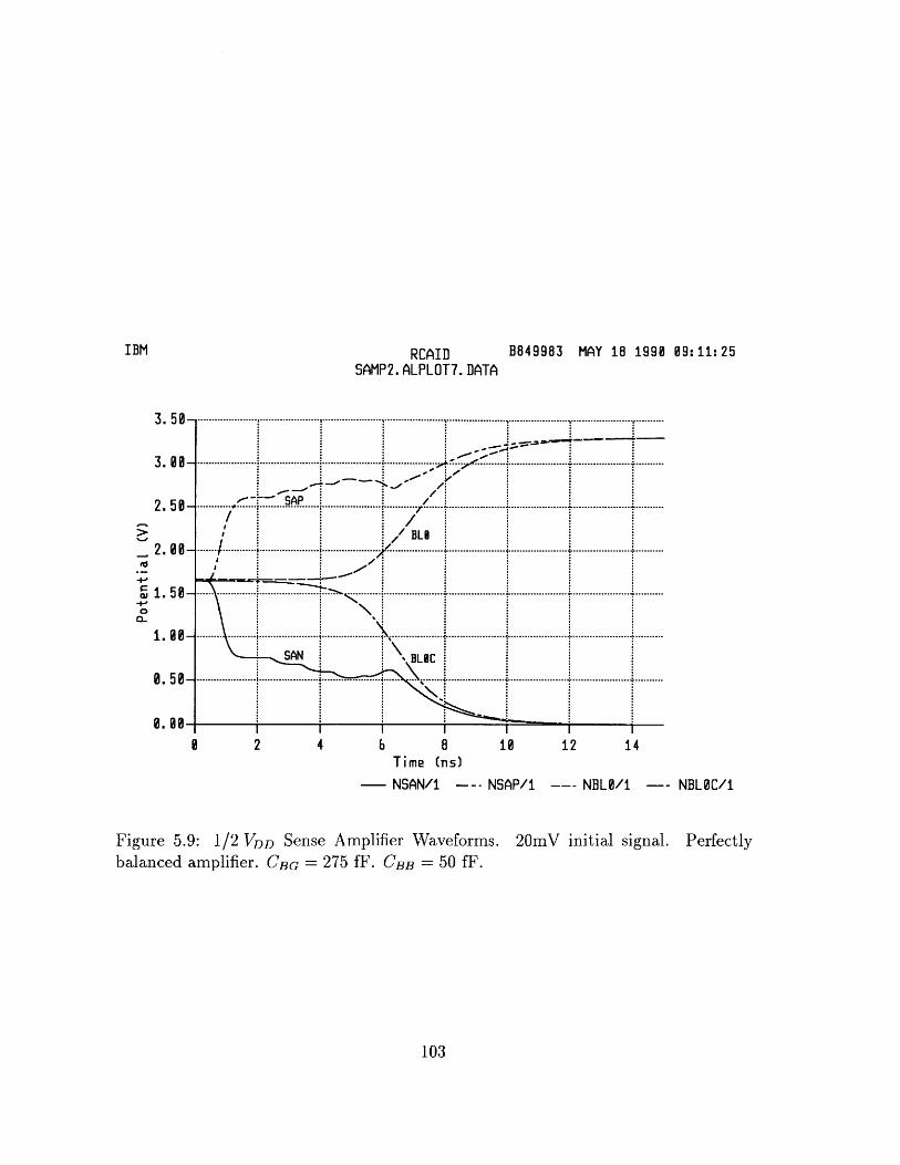
IBM RCAID B849983 MAY 18 1990 09:11:25SAMP2.ALPLOT7.DATA
3.58 .................................... ...... ...... ........
3.8
2.58 / SAP2..
OBL
CL
~1.5
o ..
SANN/ ,- BLOC - NL/i NLO
8 2 4 6 8 18 12 14Time (ns)
NSAN/1 - NSAP/1 --- NBL8/1 -- NBL8C/1
Figure 5.9: 1/2 VDD Sense Amplifier Waveforms. 20mV initial signal. Perfectlybalanced amplifier. CBG = 275 fF. CBB = 50 fF.
103
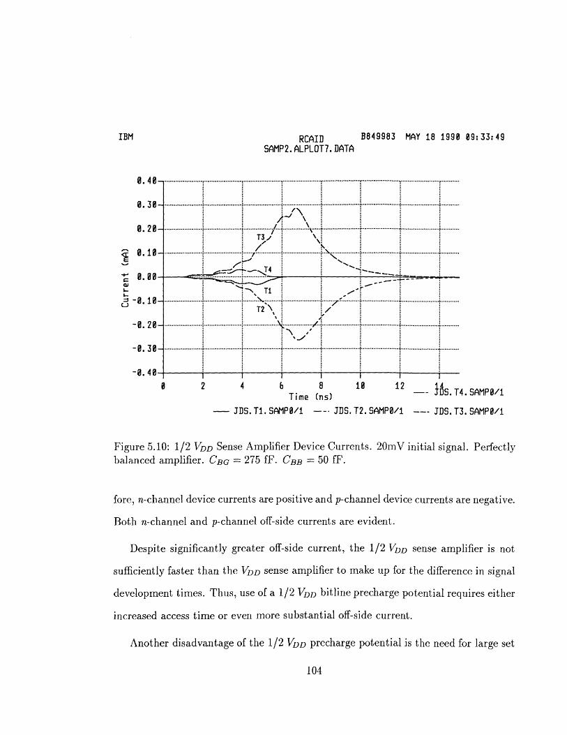
IBM RCAID 8849983 MAY 18 1990 09:33:49SAMP2.ALPLOT7.DATA
8.4
8.38
8.28
oJ
0.
-.
T3
V
8 2 b 18 2 l~S.T.S~T4/
Tieins
20-2
-0.4
0 2 4 6 8 10 12 16.4.AP/Time (ns)
JDS.Ti. SAMPO/1 --- JDS.T2.SAMPO/1 JDS.T3.SAMPO/1
Figure 5.10: 1/2 VDD Sense Amplifier Device Currents. 20mV initial signal. Perfectlybalanced amplifier. CBG = 275 fF. CBB = 50 fF.
fore, n-channel device currents are positive and p-channel device currents are negative.
Both n-channel and p-channel off-side currents are evident.
Despite significantly greater off-side current, the 1/2 VDD sense amplifier is not
sufficiently faster than the VDD sense amplifier to make up for the difference in signal
development times. Thus, use of a 1/2 VDD bitline precharge potential requires either
increased access time or even more substantial off-side current.
Another disadvantage of the 1/2 VDD precharge potential is the need for large set
104

devices to drive two shared latch nodes, SAN and SAP. Once initial amplification
is complete, the bitlines should be driven as quickly as possible to the '0' and '1'
potentials, maximizing amplifier speed. The rate at which the bitline potentials
can be changed is limited by the size of the set devices. To achieve 11 ns signal
amplification, it was necessary to employ somewhat larger n-channel SAN set devices
than were used in the VDD sense amplifier. More importantly, p-channel SAP set
devices, approximately three times larger than the n-channel SAN devices, were
needed. These devices require substantial additional layout area.
Bitline segment precharge poses an undesirable tradeoff. Bitlines can be precharged
without using a voltage generator by equalizing the bitline potentials. However, if
the bitlines are equalized at the end of the cycle, they may float above or below
1/2 VDD before the next cycle, disrupting amplifier operation. If they are equalized
at the beginning of the cycle, equalization will likely delay wordline activation. In
4M and 16M DRAMs, precharge voltage generators are often employed. They require
additional layout area and power.
5.3.3 2/3 VDD Sense Amplifier
A sense amplifier designed for use with a 2/3 VDD bitline precharge potential is shown
in Figure 5.11. The circuit is based on the n-channel array sense amplifier used in
the NTT 16M DRAM [74].
Important aspects of the 2/3 VDD sense amplifier are similar to the 1/2 VDD sense
amplifier. Though initial sensing could be performed using only the n-channel cross-
coupled pair, both cross-coupled pairs are activated simultaneously to achieve ade-
quate speed. As a result, sensitivity considerations warrant relatively wide and long
n-channel and p-channel cross-coupled pair devices.
The precharge and equalization device overdrives during the precharge interval
105
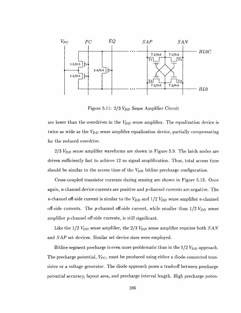
VPC PC EQ SAP SAN
7.2/0.6 7.2/0.6 BLOC
1.5/0.5
2.4/0.5
1.5/0.5
T2 _L,_ T47.2/0.6 7.2/0.6
BLO
Figure 5.11: 2/3 VDD Sense Amplifier Circuit
are lower than the overdrives in the VDD sense amplifier. The equalization device is
twice as wide as the VDD sense amplifier equalization device, partially compensating
for the reduced overdrive.
2/3 VDD sense amplifier waveforms are shown in Figure 5.9. The latch nodes are
driven sufficiently fast to achieve 12 ns signal amplification. Thus, total access time
should be similar to the access time of the VDD bitline precharge configuration.
Cross-coupled transistor currents during sensing are shown in Figure 5.13. Once
again, n-channel device currents are positive and p-channel currents are negative. The
n-channel off-side current is similar to the VDD and 1/2 VDD sense amplifier n-channel
off-side currents. The p-channel off-side current, while smaller than 1/2 VDD sense
amplifier p-channel off-side currents, is still significant.
Like the 1/2 VDD sense amplifier, the 2/3 VDD sense amplifier requires both SAN
and SAP set devices. Similar set device sizes were employed.
Bitline segment precharge is even more problematic than in the 1/2 VDD approach.
The precharge potential, Vpc, must be produced using either a diode-connected tran-
sistor or a voltage generator. The diode approach poses a tradeoff between precharge
potential accuracy, layout area, and precharge interval length. High precharge poten-
106

IBM RCAID B849983 MAY 18 1990 09:16: 50SAMP3.ALPLOT7.DATA
3.50-.... .............
r SAP
2I
_2.00-
-
1.88-
8.58-
-SAN
0 2 4 b 8 10 12 14Time (ns)
--NSAN/1 ---- NSAP/1 --- NBLO/i -- NBLOC/1
Figure 5.12: 2/3 VDD Sense Amplifier Waveforms. 20mV initial signal. Perfectlybalanced amplifier. CBG = 275 fF. CBB = 50 fF.
107
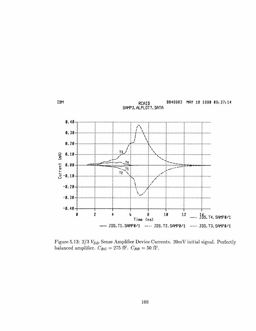
.
IBM RCAID B849983 MAY 18 1990 09:37:14SAMP3.ALPLOT7.DATA
8.4
0.38 ............... .... ....
0.28 ....... /..........
T3
T0
P 0.0. ...... .........
8 2 4 6 8 18 12 ___ .T4.SAMP/1Time (ns)
-JDS.TI.SAMPO/i - JDS.T2.SAMP8/1 JDS.T3.SAMPO/i
Figure 5.13: 2/3 VDD Sense Amplifier Device Currents. 2OmV initial signal. Perfectlybalanced amplifier. CBG = 275 fF. CBB =50 fF.
108

tial accuracy requires a large layout area to increase diode device width and/or a long
precharge interval. Using a voltage generator would likely require very high current
in order to provide the needed current driving capability.
Dhong et al. [75] proposed alternative precharge circuitry. In their circuit, the
p-channel precharge devices are replaced by n-channel devices and the VpC node is
tied to VDD. The bitlines are precharged through the n-channel devices, producing
the necessary threshold drop. A tradeoff exists between n-channel precharge potential
accuracy, n-channel precharge device area, and precharge interval length. Mismatches
between n-channel precharge devices in different columns may cause precharge po-
tential variations, resulting in reduced amplifier sensitivity due to effective timing
skews.
5.3.4 Design Impacts
Use of a VDD bitline precharge potential in 64M p-channel array DRAMs offers several
important advantages:
9 Faster signal development. Earlier transfer device turn-on and greater transfer
device overdrive speed signal development. As a result, sensing speed may be
reduced and/or access time may be improved. Slower sensing decreases power
dissipation due to off-side current and improves sense amplifier sensitivity.
* Primary amplification is performed entirely by the n-channel cross-coupled pair.
The p-channel cross-coupled devices need not be optimized for sensitivity, saving
layout area. In addition, the source of the p-channel cross-coupled pair may be
tied directly to VDD, avoiding the extra area, power, and complexity required
by p-channel cross-coupled pair latch node set circuitry.
109

e Large precharge and equalization device overdrive and fast device activation.
The maximum device overdrive is equal to VDD - VT- Devices begin conducting
after the clock potentials drops just +1 VT below VDD- Smaller precharge
and equalization devices may be used and/or the precharge interval may be
shortened. Smaller devices limit equalization and precharge clock loads, saving
clock driver area and power, and reduce sense amplifier area.
e A supply potential is used for the bitline precharge potential. No additional
circuitry is required to generate the bitline precharge potential, saving area and
power without compromising precharge potential stability.
Traditional advantages of a 1/2 VDD precharge potential in CMOS DRAMs are
mostly lost when the approach is applied to 64M DRAM sense amplifiers. Reductions
in peak current and dI/dt due to limited bitline swing are offset by increases in current
and dI/dt due to the faster amplification required to compensate for slow signal
development. Reductions in bitline charging and discharging power are offset by
additional power dissipation due to increased off-side current, additional set device
clocking, and possible use of a bitline precharge voltage generator. Finally, while
dummy cells are not required to provide a reference potential, elimination of dummy
cells creates a capacitance mismatch during sensing and increases susceptibility to
precharge voltage fluctuations.
A potential advantage of a 1/2 VDD precharge voltage is the equality of the positive
and negative bitline potential swings. This equality minimizes variations in plate and
bulk potentials induced by bitline potential swings. Plate noise is especially significant
when a high impedance plate voltage generator is employed [87]. However, if the plate
is tied to a supply potential, the noise may not be very substantial, relative to other
noise sources.
110

A 2/3 VDD precharge potential can be viewed as a compromise between VDD and
1/2 VDD bitline precharge potentials. It provides faster signal development, larger
precharge and equalization device overdrives, and quicker precharge device activation
than the 1/2 VDD precharge potential. However, it also requires more bitline charging
and discharging current and does not achieve perfectly balanced bitline swing.
2/3 VDD sense amplifiers, like 1/2 VDD sense amplifiers require set devices for
both the n-channel and p-channel cross-coupled pair source nodes. Also, to achieve
adequate speed, both n-channel and p-channel devices must participate in sensing.
Finally, bitline precharge potential generation is quite problematic.
A full VDD precharge potential seems most appropriate for 64M p-channel array
DRAM sense amplifiers. The same general arguments support use of ground for the
precharge potential in n-channel array DRAMs. Signal development is faster, though
the absolute differences in signal development time are not quite as large as the
p-channel array differences. Primary amplification is performed using only one cross-
coupled pair. Larger equalization and precharge device overdrive and quicker device
turn-on are achieved. With p-channel arrays, this advantage is somewhat offset by the
substitution of n-channel precharge and equalization devices when using a 1/2 VDD
precharge potential. With n-channel arrays, the advantage is not so diluted. Finally,
a supply potential is used for the bitline precharge potential.
Precharging n-channel array bitlines to VDD would allow use of n-channel sense
amplifier devices for primary amplification. However, signal development would be
much too slow in 64M DRAMs. When sensing a '0,' the transfer devices would oper-
ate in a slow source-follower fashion. In an n-channel array, lower bitline precharge
potentials result in faster transfer device activation and higher transfer devices over-
drive.
- __Amw_ __ - __ - 01-4
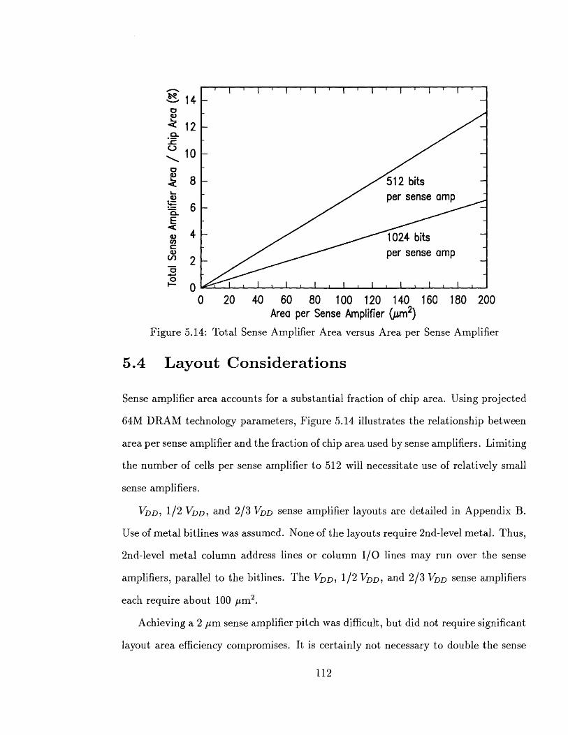
S14
12
10C-)
8 -512 bitsper sense arnp
6 --E
4 -- 1024 bitsper sense amp
0
0 20 40 60 80 100 120 140 160 180 200Area per Sense Amplifier (Im2)
Figure 5.14: Total Sense Amplifier Area versus Area per Sense Amplifier
5.4 Layout Considerations
Sense amplifier area accounts for a substantial fraction of chip area. Using projected
64M DRAM technology parameters, Figure 5.14 illustrates the relationship between
area per sense amplifier and the fraction of chip area used by sense amplifiers. Limiting
the number of cells per sense amplifier to 512 will necessitate use of relatively small
sense amplifiers.
VDD, 1/2 VDD, and 2/3 VDD sense amplifier layouts are detailed in Appendix B.
Use of metal bitlines was assumed. None of the layouts require 2nd-level metal. Thus,
2nd-level metal column address lines or column I/O lines may run over the sense
amplifiers, parallel to the bitlines. The VDD, 1/2 VDD, and 2/3 VDD sense amplifiers
each require about 100 im2 .
Achieving a 2 pm sense amplifier pitch was difficult, but did not require significant
layout area efficiency compromises. It is certainly not necessary to double the sense
112
amplifier layout pitch by placing complete sense amplifiers on both sides of the arrays.
Nor does such an approach seem desirable. Twice as many sense amplifier signal buses
and signal drivers would be required. In addition, column decode circuitry would be
needed on both sides of the arrays.
In 256M and higher density DRAMs, the bitline pitch may be so small relative to
feature sizes that sense amplifiers cannot fit within two bitline pitches. Fortunately,
64M DRAM sense amplifiers can fit within two bitline pitches.
The small sense amplifier pitch does impose some important design limitations. To
avoid using 2nd-level metal, bitline precharge devices and column I/O circuitry must
be placed on opposite sides of the arrays. Also, unless 2nd-level metal is employed to
distribute the bitline precharge potential, precharge device widths are limited by the
sense amplifier pitch. This constraint is especially significant when using a 1/2 VDD
or 2/3 VDD precharge potential since the precharge device overdrives are relatively
small.
5.5 Isolation Devices
Isolation devices do not seem desirable in 64M DRAMs. The traditional purpose of
isolation devices is to separate the active cross-coupled pair(s) from the large bitline
capacitances during initial sensing. If the bitline capacitance is very large, isolation
devices may significantly improve amplifier speed and sensitivity. However, in 64M
DRAMs, processing technology features make isolation device usage inappropriate.
As shown in Appendix B, including one isolation device per bitline segment would
require over 12 [m 2 of area per sense amplifier. If this area were taken from one of
the cross-coupled pairs, device widths would have to be decreased by 3 [pm. Thus,
potential benefits of isolation devices must be weighed against a large layout area
cost.
113
Isolation device clock loads should be roughly comparable to wordline loads. Thus,
in 64M DRAMs, isolation device clock delays will be significant, decreasing DRAM
speed.
Employment of isolation devices in 64M DRAMs requires either using an unde-
sirable intermediate bitline precharge potential or bootstrapping the isolation device
clock. If a VDD bitline precharge potential and n-channel isolation devices are em-
ployed, the isolation device clock potential must be bootstrapped above VDD during
signal development. If p-channel isolation devices are employed, the isolation device
clock potential must be bootstrapped below ground to restore full '0' potentials. Sim-
ilarly, if bitlines are precharged to ground, p-channel isolation device clocks must be
bootstrapped below ground during signal development and n-channel isolation device
clocks must be bootstrapped above VDD during cell restoration.
Decreasing the effective capacitance between cross-coupled pair signal nodes and
ground will not always improve performance. In 64M DRAMs with only 256 cells per
bitline segment, total bitline capacitance is not particularly large. Isolating cross-
coupled pair from the bitline segments will not only decrease total effective signal
node capacitance, but will also effect the ratio of the coupling capacitance between
the signal nodes and the latch nodes to the capacitance between the signal node and
ground.
As processing technology improves, gate capacitances generally increase relative
to diffusion capacitances. Decreases in gate insulator thickness increase gate capaci-
tances. Increases in bulk doping increase diffusion capacitances, but the dependence
is not nearly as strong as the gate capacitance dependence on insulator thickness.
Improved isolation techniques reduce the perimeter components of diffusion capaci-
tances. In 64M DRAMs, sense amplifier diffusion capacitances will likely be small
relative to gate capacitances. Thus, if isolation devices are employed, the ratio of
114
cross-coupled pair gate-source capacitances to the parasitic capacitance between the
signal nodes and ground will be quite large. As a result, during primary sensing the
change in the off-side signal potential due to gate-source coupling will be substantial.
Unless both the n-channel and p-channel cross-coupled pairs are isolated from
the bitlines, a full VDD signal cannot be developed until after the isolation devices
are turned on. But if both n-channel and p-channel cross-coupled pairs are isolated,
the isolation device clock must be bootstrapped to allow restoration of full VDD and
ground stored potentials.
The VDD sense amplifier was simulated assuming complete isolation of the bitlines
and the p-channel cross-coupled pair from the n-channel cross-coupled pair. Parasitic
diffusion capacitances were derived from the layout. The resulting waveforms are
shown in Figure 5.15. The high signal potential drops by roughly a factor of two.
As a result of the large high signal potential reduction, the overdrive on the
n-channel cross-coupled pair as the isolation devices are turned on is very small. If n-
channel isolation devices are employed, the device separating the low potential signal
node and the low potential bitline will turn on before the opposite isolation device.
Because cross-coupled pair overdrive is small, the isolation devices must be activated
very slowly to keep the low signal node potential below VT, avoiding significant off-side
current.
The benefits of isolation device use in 64M DRAM sense amplifiers are question-
able at best. The costs include increased sense amplifier area, extra clock timing
and driver circuits, and decreased sensing speed due to isolation device clock delays.
Thus, isolation devices should be avoided.
115
5.6 Sensitivity Analysis
The sensitivity of the VDD sense amplifier was examined. Three aspects of sensitivity
were considered: the minimum overdrive voltage required, given a perfectly balanced
amplifier; offset due to process variations; and offset due to bitline-to-bitline coupling.
Figure 5.16 shows the final bitline segment potential difference versus the initial
signal presented to the sense amplifier. A worst case uniform pattern was assumed.
A 3 mV overdrive is sufficient to achieve adequate amplification.
Figure 5.17 shows the average off-side current per sense amplifier assuming a 100 ns
cycle and a worst case uniform pattern. If 16K sense amplifiers are active, 10 mV
sense amplifier overdrives will limit total average DRAM off-side current to less than
35 mA.
Sense amplifier offset due to transistor gain and bitline capacitance mismatches
was analyzed using both best and worst case uniform patterns. All columns had
equally unbalanced sense amplifiers and bitlines. Results are presented in Figures 5.18
and 5.19.
As expected, offsets due to gain and capacitance mismatches are roughly propor-
tional to the gain and capacitance mismatch percentages. Interestingly, bitline-to-
bitline coupling has a large impact on the resulting offsets.
Increasing cross-coupled pair transistor currents decreases Gm/I, worsening offset
due to transistor gain and bitline capacitance mismatches. Because the latch node
set devices are shared by many sense amplifiers, currents during amplification are
pattern dependent. If the pattern includes only a few '1's and many '0's, the latch
node potential will fall quickly until it reaches VBLR - VT. As a result, currents in
the amplifiers sensing '1's will be higher than usual. The worst case pattern is shown
in Figure 5.20. A small group of '1's are present in the middle of a field of '0's.
116
Bitline-to-bitline coupling may aid detection of the '1's next to '0's. Thus, the inner
'1's are most vulnerable.
In order to minimize this effect, the latch node is initially pulled down by relatively
small devices. Given a uniform pattern, off-side current actually increases about 1-
2 ns after the cross-coupled pairs begin conducting. Computer simulation showed
only a slight difference in offset under a worst case uniform pattern and offset under
the worst case non-uniform pattern shown in Figure 5.20.
Bitline-to-bitline coupling during signal amplification introduces an offset. The
offset of an individual amplifier depends on the signals presented to surrounding am-
plifiers. Figure 5.21 illustrates patterns used for coupling induced offset analysis. In
the best case patterns, the high bitline segment potentials are equal. Thus, ampli-
fication will begin simultaneously in all amplifiers. In the worst case pattern, the
low potentials are equal. Amplification will begin in the surrounding sense amplifiers
before amplification begins in an amplifier presented with a marginal signal.
Figure 5.22 shows results of computer simulations. Bitline-to-bitline coupling
during signal amplification results in very significant sense amplifier offset, especially
when a single marginal signal is surrounded by strong signals and when the high
bitline potentials differ.
117
-!= " ! ! !!
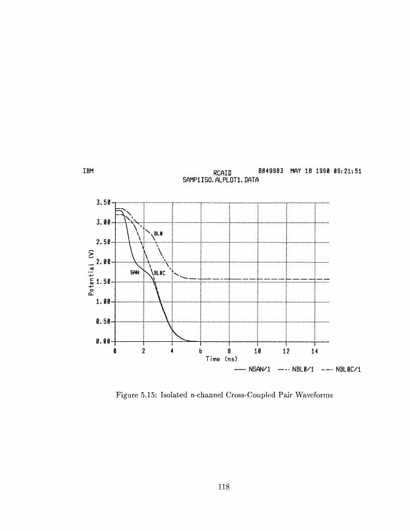
RCAID B849983 MAY 18 1990 09:21:51SAMPiISO.ALPLOTI.DATA
0 2 4 b 8 18 12 14Time (ns)
NSAN/1 --- NBLO/1 --- NBLOC/1
Figure 5.15: Isolated n-channel Cross-Coupled Pair Waveforms
118
IBM
3.50
3.
2.
2.
1.
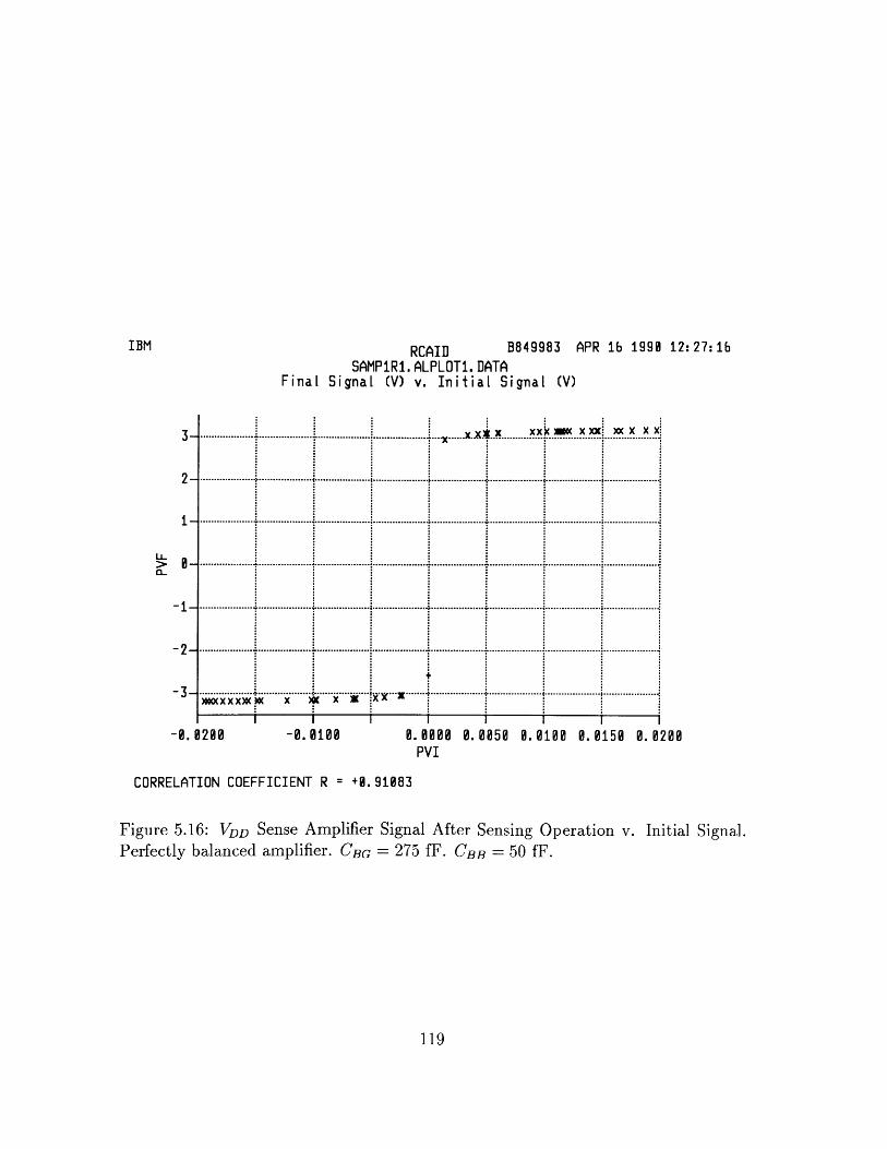
IBM RCAID B849983 APR lb 1990 12:27:1bSAMPiRI.ALPLOTI.DATA
Final Signal (V) v. Initial Signal (V)
Xx XW XX XXX Xx X X X:
3 xXXX.X.......>..
IPVI
CRRELA COEFFICIENT R. = .+..91.83
Perfectl baacdamlf. 0 CBG = 00 270f . CB0=50 f. M .05 .00
>0VCRATINCEFCETR=-.18
-iue51:l DSneA piirSga ftrSnigOeainv nta inl
-2fcl aacdapiir.CG=25f.CB-5 F
119
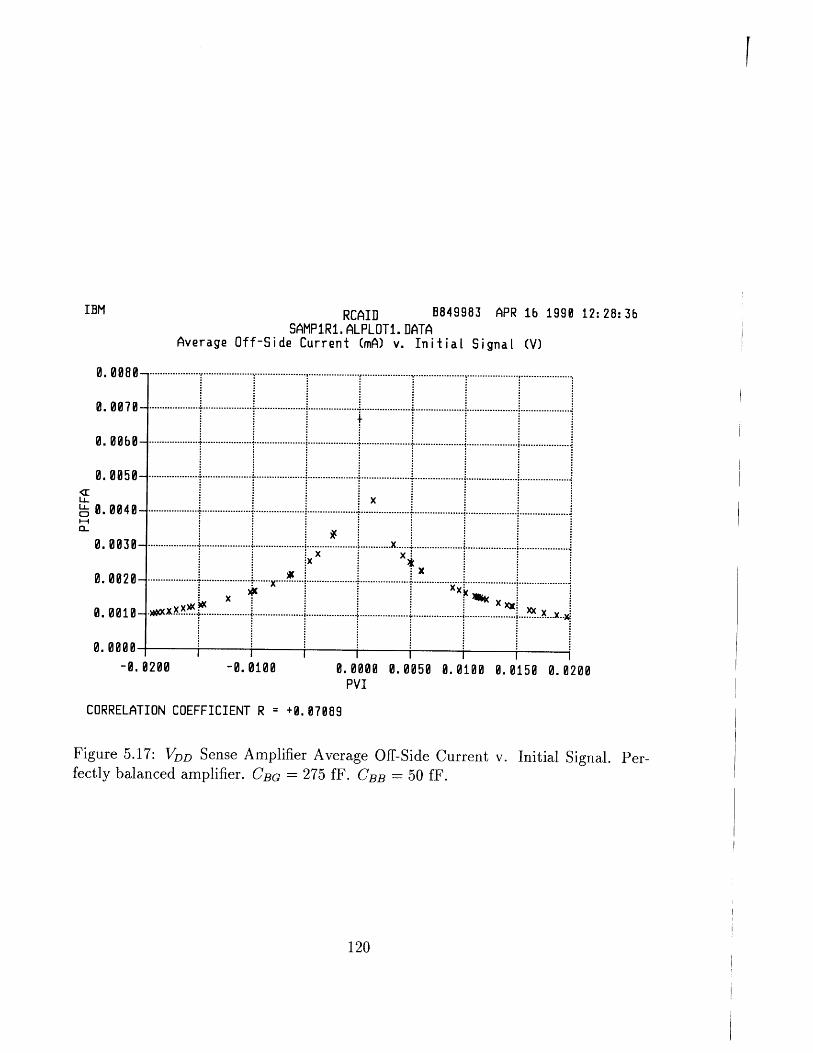
RCAID B849983 APR lb 1990SAMPIRI.ALPLOTI.DATA
Average Off-Side Current (mA) v. Initial Signal (V)
......................................
X X.
x xx * X
oXXW .)Q0(X.Xx X
0. 0080-
0. 0070-
0. 00b-
0. 0050-
0. 0040-
0. 0030-
0. 0020-
0. 0010-
0. 0000-
-0. 0200 -0. Koo0I IIIII
0.0000 0.0050 0.0100 0.0150 0.0200PVI
CORRELATION COEFFICIENT R = +0.07089
Figure 5.17: VDD Sense Amplifier Average Off-Side Current v. Initial Signal. Per-fectly balanced amplifier. CBG = 275 fF. CBB = 50 fF.
120
AI
IBM 12: 28: 3b

E
Ca,
V
0 5 10 15 20N-channel # Mismatch (%)
Figure 5.18: VDD Sense Amplifier Offset due to Transistor Gain Mismatch
E
ca,
0 5 10 15 20Bitline Capacitance Mismatch (%)
Figure 5.19: VDD Sense Amplifier Offset due to Bitline Capacitance Mismatch
121
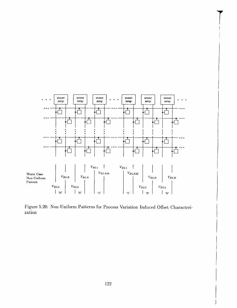
T
sense sense sense sense sense senseamp amp amp amp amp amp
fI 4rVBL1 I
VBLRM
VBLR VBLR
VBLO VBLO
' 'O' '1'
VBLRM
VBLR VBLR
VBLO VBLO
'1' ' 'O'
Figure 5.20: Non-Uniform Patterns for Process Variation Induced Offset Characteri-zation
122
Worst CaseNon-UniformPattern
_n0 & .
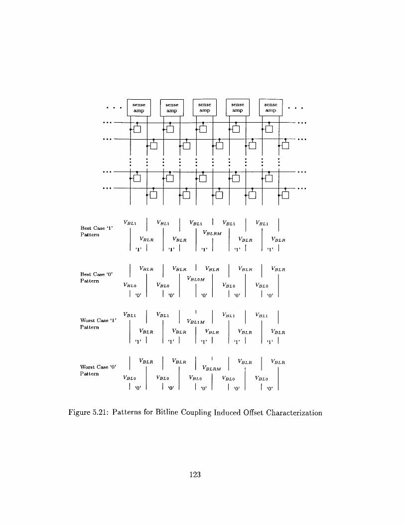
sense sense sense sense senseamp amp amp amp amp
VBL1 VBL1 VBL1 VB 1 VBL1Best Case '1'Pattern VBLRM
VBLR VBLR VBLR VBLR
'1' '1' i '1' I '1' I '1' I
Best Case '' VBLR VBLR VBLR VBLR VBLR
Pattern VBLOMVBLO VBLO VBLO VBLO
I 'o' ' ' '0 ' '0 ' 1
Worst Case '1'Pattern
Worst Case '0'Pattern
VBL1 VBL1 VB1 VBL1| VBL1M |
VBLR VBLR VBLR VBLR VBLR
'1' I '1' I '1' I'1' I'1' I
VBLR VBLR VBLR VBLRVBL RM ||
VBLO VBLO VBLO VBLO VBLO
I 'o' 1 '0' 1 '0' I '0' 1 '0'
Figure 5.21: Patterns for Bitline Coupling Induced Offset Characterization
123
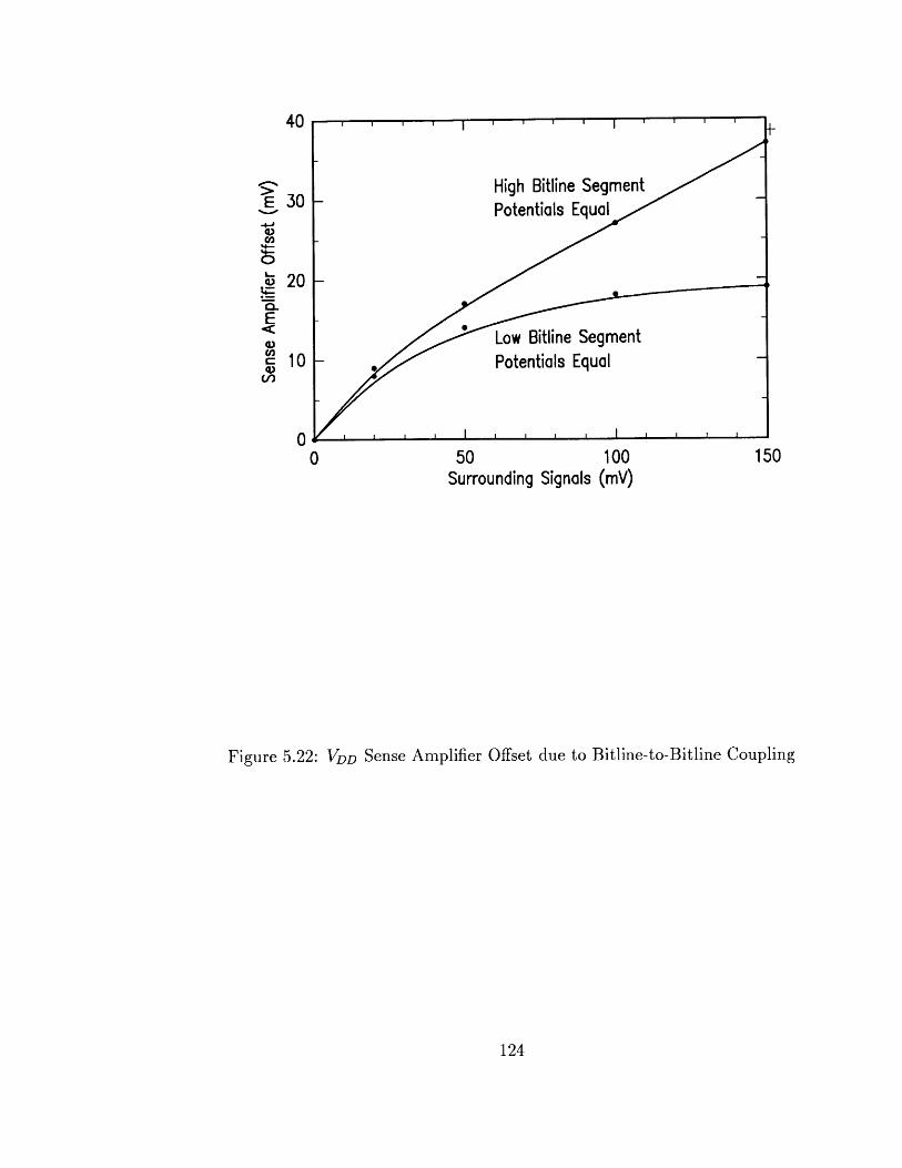
- U
40
High Bitline SegmentE 30 ~Potentials Equal
20a.
E< Low Bitline Segment
c 10 Potentials Equal
0 50 100 150Surrounding Signals (mV)
Figure 5.22: VDD Sense Amplifier Offset due to Bitline-to-Bitline Coupling
124
Chapter 6
Conclusion
6.1 Major Accomplishments
Sense amplifier operation has been studied analytically. Signal node coupling effects
were included in an optimal latching pulse derivation. Effects of process variations
on sense amplifier sensitivity have been studied.
Sense amplifiers used in each major one-transistor cell DRAM generation have
been analyzed. Processing technology evolution has had a major impact on sense
amplifier designs. The merits of particular design approaches are critically dependent
on the technology employed.
Using technology and performance projections, 64M DRAM sense amplifier design
issues have been examined. Several important conclusions have been drawn:
* Intrinsic bitline charging and discharging power dissipation is extremely impor-
tant. To limit this power, each bitline segment should include only 256 cells.
* In n-channel array DRAMs, bitline segments should be precharged to ground.
In p-channel array DRAMs, segments should be precharged to VDD-
e Isolation devices should not be employed.
125
6.2 Future Work
Effects of bitline-to-bitline coupling on sense amplifier sensitivity are extremely impor-
tant. Yet available analyses are incomplete. The effects of bitline-to-bitline coupling
on offset induced by process variations has not been sufficiently explored. In addi-
tion, effects of sense amplifier design parameters and signal patterns may be more
completely characterized. Finally, the twisted bitline architecture should be carefully
evaluated, paying particular attention to the added layout area and process complex-
ity required.
126
References
[1] R. H. Dennard, "Field-effect transistor memory,". U.S. Patent 3 387 286, June4, 1968.
[2] L. Cohen, R. Green, K. Smith, and J. L. Seely, "Single-transistor cell makesroom for more memory on an MOS chip," Electronics, vol. 44, pp. 69-75, Aug.1971.
[3] L. Boonstra, C. W. Lambrechtse, and R. H. W. Salters, "A 4096-b one-transistorper bit random-access memory with internal timing and low dissipation," IEEEJournal of Solid State Circuits, vol. SC-8, pp. 305-310, Oct. 1973.
[4] C. W. Lambrechtse, R. H. W. Salters, and L. Boonstra, "A 4096 bit one-transistor per-bit RAM with internal timing and low dissipation," in IEEE In-ternational Solid-State Circuits Conference Digest of Technical Papers, pp. 26-27,194, Feb. 1973.
[5] R. Proebsting and R. Green, "A TTL compatible 4096-bit N-channel RAM," inIEEE International Solid-State Circuits Conference Digest of Technical Papers,pp. 28-29, Feb. 1973.
[6] K. U. Stein, A. Sihling, and E. Doering, "Storage array and sense/refresh circuitfor single-transistor memory cells," in IEEE International Solid-State CircuitsConference Digest of Technical Papers, pp. 56-57, Feb. 1972.
[7] K. U. Stein, A. Sihling, and E. Doering, "Storage array and sense/refresh cir-cuit for single-transistor memory cells," IEEE Journal of Solid State Circuits,vol. SC-7, pp. 336-340, Oct. 1972.
[8] W. K. Hoffman and H. L. Kalter, "An 8-k bit random-access memory chip usinga one-device FET cell," in IEEE International Solid-State Circuits ConferenceDigest of Technical Papers, pp. 64-65, Feb. 1973.
[9] W. K. Hoffman and H. L. Kalter, "An 8K b random-access memory chip usingthe one-device FET cell," IEEE Journal of Solid State Circuits, vol. SC-8,pp. 298-305, Oct. 1973.
127
[10] R. C. Foss, "The design of MOS dynamic rams," in IEEE International Solid-State Circuits Conference Digest of Technical Papers, pp. 140-141, Feb. 1979.
[11] I. Lee, R. T. Yu, F. J. Smith, S. Wong, and M. P. Embrathiry, "A 64Kb MOSdynamic RAM," in IEEE International Solid-State Circuits Conference Digestof Technical Papers, pp. 146-147, Feb. 1979.
[12] F. J. Smith, R. T. Yu, I. Lee, S. S. Wong, and M. P. Embrathiry, "A 64 kbitMOS dynamic RAM with novel memory capacitor," IEEE Journal of SolidState Circuits, vol. SC-15, pp. 184-189, Apr. 1980.
[13] D. V. Essel, R. Losehand, and B. Rehn, "A 64Kb VMOS RAM," in IEEE Inter-national Solid-State Circuits Conference Digest of Technical Papers, pp. 148-149,289, Feb. 1979.
[14] K. Itoh, R. Hori, H. Masuda, and Y. Kamigaki, "A single 5V 64K dynamicRAM," in IEEE International Solid-State Circuits Conference Digest of Tech-nical Papers, pp. 228-229, Feb. 1980.
[15] H. Masuda, R. Hori, Y. Kamigaki, K. Itoh, H. Kawamoto, and H. Katto, "A 5V-only 64K dynamic RAM based on high s/n design," IEEE Journal of SolidState Circuits, vol. SC-15, pp. 846-854, Oct. 1980.
[16] W. T. Lynch and H. J. Boll, "Optimization of the latching pulse for dynamicflip-flop sensors," IEEE Journal of Solid State Circuits, vol. SC-9, pp. 49-55,Apr. 1974.
[17] N. Ieda, E. Arai, K. Kiuchi, Y. Ohmori, and K. Takeya, "A 64K MOS RAMdesign," in Proceedings of the 9th Conference on Solid State Devices, pp. 57-63,1977.
[18] N. Ieda, Y. Ohmori, K. Takeya, and T. Yano, "Single transistor MOS RAMusing a short-channel MOS transistor," IEEE Journal of Solid State Circuits,vol. SC-13, pp. 218-224, Apr. 1978.
[19] T. Yano, N. leda, Y. Ohmori, and K. Takeya, "Highly sensitive sense circuit forsingle transistor MOS RAM," Review of The Electrical Communication Labo-ratories, vol. 27, pp. 10-17, January-February 1979.
[20] T. C. May and M. H. Woods, "Alpha-particle-induced soft errors in dynamicmemories," IEEE Transactions on Electron Devices, vol. ED-26, pp. 2-9, Jan.1979.
[21] V. L. Rideout, "One-device cells for dynamic random-access memories: a tuto-rial," IEEE Transactions on Electron Devices, vol. ED-26, pp. 839-852, June1979.
128
[22] S. Asai, "Trends in megabit DRAMs," in International Electron Devices MeetingTechnical Digest, pp. 6-12, Dec. 1984.
[23] H. Sunami and S. Asai, "Trends in megabit DRAM's," in Proceedings of the In-ternational Symposium on VLSI Technology, Systems, and Applications, pp. 4-8, 1985.
[24] H. Sunami, "Cell structures for future DRAM's," in International Electron De-vices Meeting Technical Digest, pp. 694-697, Dec. 1985.
[25] W. P. Noble and W. W. Walker, "Fundamental limitations on DRAM storagecapacitors," IEEE Circuits and Devices Magazine, vol. 1, pp. 45-51, Jan. 1985.
[26] N. C. C. Lu, "Advanced cell structures for dynamic RAMs," IEEE Circuits andDevices Magazine, vol. 5, pp. 27-36, Jan. 1989.
[27] H. E. Maes, G. Groeseneken, H. Lebon, and J. Witters, "Trends in semicon-ductor memories," Microelectronics Journal, vol. 20, no. 1-2, pp. 9-58, 1989.
[28] K. Natori, "Sensitivity of dynamic MOS flip-flop sense amplifiers," IEEE Trans-actions on Electron Devices, vol. ED-33, pp. 482-488, Apr. 1986.
[29] R. Kraus, "Analysis and reduction of sense-amplifier offset," IEEE Journal ofSolid State Circuits, vol. 24, pp. 1028-1033, Aug. 1989.
[30] P. R. Gray and R. G. Meyer, Analysis and Design of Analog Integrated Circuits.John Wiley & Sons, second ed., 1984.
[31] C. Kuo, N. Kitagawa, E. Ward, and P. Drayer, "Sense amplifier design is keyto 1-transistor cell in 4,096-bit RAM," Electronics, vol. 46, pp. 116-121, Sep.1973.
[32] R. Foss and R. Harland, "Simplified peripheral circuits for a marginally testable4K RAM," in IEEE International Solid-State Circuits Conference Digest ofTechnical Papers, pp. 102-103, Feb. 1975.
[33] R. C. Foss and R. Harland, "Peripheral circuits for one-transistor cell MOSRAM's," IEEE Journal of Solid State Circuits, vol. SC-10, pp. 255-261, Oct.1975.
[34] C. N. Ahlquist, J. R. Breivogel, J. T. Koo, J. L. McCollum, W. G. Oldham, andA. L. Renninger, "A 16K dynamic RAM," in IEEE International Solid-StateCircuits Conference Digest of Technical Papers, pp. 128-129, Feb. 1976.
[35] C. N. Ahlquist, J. R. Breivogel, J. T. Koo, J. L. McCollum, W. G. Oldham,and A. L. Renninger, "A 16 384-bit dynamic RAM," IEEE Journal of SolidState Circuits, vol. SC-11, pp. 570-574, Oct. 1976.
129
[36] J. E. Coe and W. G. Oldham, "Enter the 16,384-bit RAM," Electronics, vol. 49,pp. 116-121, Feb. 1976.
[37] P. R. Schroeder and R. J. Proebsting, "A 16K x 1 bit dynamic RAM," inIEEE International Solid-State Circuits Conference Digest of Technical Papers,pp. 12-13, Feb. 1977.
[38] R. Proebsting, "Dynamic MOS RAM's," in International Conference on Com-munications Conference Record, pp. 147-150, June 1977.
[39] D. Coker, "16K - the new generation dynamic RAM," in Electro/77 ConferenceRecord, p. 5/3, 1977.
[40] R. P. Cenker, D. G. Clemons, W. R. Huber, J. B. Petrizzi, F. J. Procyk, andG. M. Trout, "A fault-tolerant 64K dynamic RAM," in IEEE InternationalSolid-State Circuits Conference Digest of Technical Papers, pp. 150-151,290,Feb. 1979.
[41] R. P. Cenker, D. G. Clemons, W. R. Huber, J. B. Petrizzi, F. J. Procyk, andG. M. Trout, "A fault-tolerant 64K dynamic random-access memory," IEEETransactions on Electron Devices, vol. ED-26, pp. 853-860, June 1979.
[42] R. R. DeSimone, N. M. Donofrio, B. L. Flur, R. H. Kruggel, and H. H. Leung,"FET RAMs," in IEEE International Solid-State Circuits Conference Digest ofTechnical Papers, pp. 154-155,291, Feb. 1979.
[43] R. A. Larsen, "A silicon and aluminum dynamic memory technology," IBMJournal of Research and Development, vol. 24, pp. 268-282, May 1980.
[44] L. G. Heller, "Cross-coupled charge-transfer sense amplifier," in IEEE Inter-national Solid-State Circuits Conference Digest of Technical Papers, pp. 20-21,Feb. 1979.
[45] G. R. M. Rao and J. Hewkin, "64-K dynamic RAM needs only one 5-volt supplyto outstrip 16-K parts," Electronics, vol. 51, pp. 109-116, Sep. 1978.
[46] L. S. White, Jr., N. H. Hong, D. J. Redwine, and G. R. M. Rao, "A 5V-only 64Kdynamic RAM," in IEEE International Solid-State Circuits Conference Digestof Technical Papers, pp. 230-231, Feb. 1980.
[47] J. Y. Chan, J. J. Barnes, C. Y. Wang, J. M. De Blasi, and M. R. Guidry, "A100 ns 5 V only 64K x 1 MOS dynamic RAM," IEEE Journal of Solid StateCircuits, vol. SC-15, pp. 839-846, Oct. 1980.
[48] J. J. Barnes and J. Y. Chan, "A high performance sense amplifier for a 5 Vdynamic RAM," IEEE Journal of Solid State Circuits, vol. SC-15, pp. 831-839,Oct. 1980.
130
[49] P. Madland, J. Schutz, R. Green, and R. Kung, "CMOS vs. NMOS comparisonsin dynamic RAM design," in Proceedings IEEE International Conference onComputer Design: VLSI in Computers, pp. 379-382, October-November 1983.
[50] C. G. Sodini and T. I. Kamins, "Enhanced capacitor for one-transistor memorycell," IEEE Transactions on Electron Devices, vol. ED-23, pp. 1187-1189, Oct.1976.
[51] A. F. Tasch, Jr., P. K. Chatterjee, H. Fu, and T. C. Holloway, "The Hi-CRAM cell concept," in International Electron Devices Meeting Technical Digest,pp. 287-290, Dec. 1977.
[52] A. Endo, S. Ito, and M. Ishihara, "256 kbit dynamic RAM," Hitachi Review,vol. 33, pp. 61-66, Apr. 1984.
[53] A. Endo, S. Ito, and M. Ishihara, "A 256K-bit dynamic RAM with high alphaimmunity," Microelectronics Journal, vol. 15, no. 5, pp. 5-15, 1984.
[54] R. I. Kung, A. M. Mohsen, J. D. Schutz, P. D. Madland, C. C. Webb,E. R. Hamdy, C. J. Simonsen, R. T. Guo, K. K. Yu, and S. Chou, "A sub100ns 256K DRAM in CMOS III technology," in IEEE International Solid-State Circuits Conference Digest of Technical Papers, pp. 278-279,354, Feb.1984.
[55] A. Mohsen, R. Kung, J. Schutz, P. Madland, C. Simonsen, E. Hamdy, andK. Yu, "C-MOS 256-K RAM with wideband output stands by on microwatts,"Electronics, vol. 57, pp. 138-143, June 1984.
[56] A. Mohsen, R. I. Kung, C. J. Simonsen, J. Schutz, P. D. Madland, E. Z. Hamdy,and M. T. Bohr, "The design and performance of CMOS 256K bit DRAMdevices," IEEE Journal of Solid State Circuits, vol. SC-19, pp. 610-618, Oct.1984.
[57] N. C. Lu and H. H. Chao, "Half-Vdd bit-line sensing scheme in CMOSDRAM's," IEEE Journal of Solid State Circuits, vol. SC-19, pp. 451-454, Aug.1984.
[58] S. Saito, S. Fujii, Y. Okada, S. Sawada, S. Shinozaki, K. Natori, and 0. Ozawa,"A 1Mb CMOS DRAM with fast page and static column modes," in IEEE In-ternational Solid-State Circuits Conference Digest of Technical Papers, pp. 252-253, Feb. 1985.
[59] S. Saito, S. Fujii, Y. Okada, S. Sawada, S. Shinozaki, K. Natori, and 0. Ozawa,"A 1-Mbit CMOS DRAM with fast page mode and static column mode," IEEEJournal of Solid State Circuits, vol. SC-20, pp. 903-908, Oct. 1985.
131
[60] S. Fujii, S. Saito, and Y. Matsumoto, "Low-power, highspeed 1M bit CMOSDRAM," Toshiba Review International Edition, pp. 22-26, Summer 1985.
[61] J. Neal, B. Holland, S. Inoue, W. K. Loh, H. McAdams, and K. Poteet, "A 1MbCMOS DRAM with design-for-test functions," in IEEE International Solid-State Circuits Conference Digest of Technical Papers, pp. 264-265,367, Feb.1986.
[62] H. McAdams, J. H. Neal, B. Holland, S. Inoue, W. K. Loh, and K. Poteet, "A1-Mbit CMOS dynamic RAM with design-for test functions," IEEE Journal ofSolid State Circuits, vol. SC-21, pp. 635-642, Oct. 1986.
[63] T. Furuyama, T. Ohsawa, Y. Watanabe, H. Ishiuchi, T. Tanaka, K. Ohuchi,H. Tango, K. Natori, and 0. Ozawa, "An experimental 4Mb CMOS DRAM," inIEEE International Solid-State Circuits Conference Digest of Technical Papers,pp. 272-273,370, Feb. 1986.
[64] T. Furuyama, T. Ohsawa, Y. Watanabe, H. Ishiuchi, T. Watanabe, T. Tanaka,K. Natori, and 0. Ozawa, "An experimental 4-Mbit CMOS DRAM," IEEEJournal of Solid State Circuits, vol. SC-21, pp. 605-611, Oct. 1986.
[65] M. Aoki, S. Ikenaga, Y. Nakagome, M. Horiguchi, Y. Kawase, Y. Kawamoto,and K. Itoh, "New DRAM noise generation under half-vcc precharge and itsreduction using a transposed amplifier," IEEE Journal of Solid State Circuits,vol. 24, pp. 889-894, Aug. 1989.
[66] Y. Nakagome, M. Aoki, S. Ikenaga, M. Horiguchi, S. Kimura, Y. Kawamoto,and K. Itoh, "The impact of data-line interference noise on DRAM scaling,"IEEE Journal of Solid State Circuits, vol. 23, pp. 1120-1127, Oct. 1988.
[67] Y. Konishi, M. Kumanoya, H. Yamasaki, K. Dosaka, and T. Yoshihara, "Anal-ysis of coupling noise between adjacent bit lines in megabit DRAM's," IEEEJournal of Solid State Circuits, vol. 24, pp. 35-42, Feb. 1989.
[68] M. Aoki, Y. Nakagome, M. Horiguchi, H. Tanaka, S. Ikenaga, J. Etoh,Y. Kawamoto, S. Kimura, E. Takeda, H. Sunami, and K. Itoh, "A 60-ns 16-Mbit CMOS DRAM with a transposed data-line structure," IEEE Journal ofSolid State Circuits, vol. 23, pp. 1113-1119, Oct. 1988.
[69] T. Yoshihara, H. Hidaka, Y. Matsuda, and K. Fujishima, "A twisted bit linetechnique for multi-Mb DRAMs," in IEEE International Solid-State CircuitsConference Digest of Technical Papers, pp. 238-239, Feb. 1988.
[70] M. Aoki, Y. Nakagome, M. Horiguchi, S. Ikenaga, J. Etoh, Y. Kawamoto,S. Kimura, E. Takeda, H. Sunami, and K. Itoh, "An experimental 16Mb DRAM
132
with transposed data-line structure," in IEEE International Solid-State CircuitsConference Digest of Technical Papers, pp. 250-251,391-392, Feb. 1988.
[71] K. Arimoto, K. Fujishima, Y. Matsuda, T. Oishi, M. Tsukude, W. Wakamiya,S. Satoh, M. Yamada, T. Yoshihara, and T. Nakano, "A 60ns 3.3V 16MbDRAM," in IEEE International Solid-State Circuits Conference Digest of Tech-nical Papers, pp. 244-245,352, Feb. 1989.
[72] K. Arimoto, K. Fujishima, Y. Matsuda, M. Tsukude, T. Oishi, W. Wakamiya,S. Satoh, M. Yamada, and T. Nakano, "A 60-ns 3.3-V-only 16-Mbit DRAM withmultipurpose register," IEEE Journal of Solid State Circuits, vol. 24, pp. 1184-1190, Oct. 1989.
[73] S. Chou, T. Takano, A. Kita, F. Ichikawa, and M. Uesugi, "A 60-ns 16-MbitDRAM with a minimized sensing delay caused by bit-line stray capacitance,"IEEE Journal of Solid State Circuits, vol. 24, pp. 1176-1183, Oct. 1989.
[74] T. Mano, T. Matsumura, J. Yamada, J. Inoue, S. Nakajima, K. Minegishi,K. Miura, T. Matsuda, C. Hashimoto, and H. Namatsu, "Circuit technologiesfor 16Mb DRAMs," in IEEE International Solid-State Circuits Conference Di-gest of Technical Papers, pp. 22-23,323-324, Feb. 1987.
[75] S. H. Dhong, N. C. Lu, W. Hwang, and S. A. Parke, "High-speed sensing schemefor CMOS DRAM's," IEEE Journal of Solid State Circuits, vol. 23, pp. 34-40,Feb. 1988.
[76] S. Fujii, M. Ogihara, M. Shimizu, M. Yoshida, K. Numata, T. Hara, S. Watan-abe, S. Sawada, T. Mizuno, J. Kumagai, S. Yoshikawa, S. Kaki, Y. Saito,H. Aochi, T. Hamamoto, and K. Toita, "A 45ns 16Mb DRAM with triple-well structure," in IEEE International Solid-State Circuits Conference Digestof Technical Papers, pp. 248-249,354, Feb. 1989.
[77] S. Fujii, M. Ogihara, M. Shimizu, M. Yoshida, K. Numata, T. Hara, S. Watan-abe, S. Sawada, T. Mizuno, J. Kumagai, S. Yoshikawa, S. Kaki, Y. Saito,H. Aochi, T. Hamamoto, and K. Toita, "A 45-ns 16-Mbit DRAM with triple-well structure," IEEE Journal of Solid State Circuits, vol. 24, pp. 1170-1175,Oct. 1989.
[78] A. F. Tasch, Jr., and L. H. Parker, "Memory cell and technology issues for64- and 256-Mbit one-transistor cell MOS DRAMs," Proceedings of the IEEE,vol. 77, pp. 374-388, March 1989.
[79] B. Hoeneisen and C. A. Mead, "Fundamental limitations in microelectronics -I. MOS technology," Solid-State Electronics, vol. 15, pp. 819-829, 1972.
133

[80] T. H. Ning, P. W. Cook, R. H. Dennard, C. M. Osburn, S. E. Schuster, andH. Yu, "1 pm MOSFET VLSI technology: part IV - hot-electron design con-straints," IEEE Journal of Solid State Circuits, vol. SC-14, pp. 268-275, Apr.1979.
[81] S. Ogura, P. J. Tsang, W. W. Walker, D. L. Critchlow, and J. F. Shepard,"Design and characteristics of the lightly doped drain-source (LDD) insulatedgate field-effect transistor," IEEE Transactions on Electron Devices, vol. ED-27,pp. 1359-1367, Aug. 1980.
[82] A. Reisman, "Device, circuit, and technology scaling to micron and submicrondimensions," Proceedings of the IEEE, vol. 71, pp. 550-565, May 1983.
[83] Joint Electron Device Engineering Council, "64Mbit DRAM power supply de-cision," News Release, Sep. 1989.
[84] H. Hidaka, K. Fujishima, Y. Matsuda, M. Asakura, and T. Yoshihara, "Twistedbit-line architectures for multi-megabit DRAM's," IEEE Journal of Solid StateCircuits, vol. 24, pp. 21-27, Feb. 1989.
[85] J. A. Fifield and H. L. Kalter, "Architecture and analysis of a crosstalk-shielded-bit-line DRAM," Burlington Technical Bulletin TR 19.90437, IBM, May 1989.
[86] M. Aoki, J. Etoh, K. Itoh, S. Kimura, and Y. Kawamoto, "A 1.5-V DRAMfor battery-based applications," IEEE Journal of Solid State Circuits, vol. 24,pp. 1206-1212, Oct. 1989.
[87] N. C. C. Lu, H. H. Chao, and W. Hwang, "Plate-noise analysis of an on-chipgenerated half-VDD biased-plate PMOS cell in CMOS DRAM's," IEEE Journalof Solid State Circuits, vol. SC-20, pp. 1272-1276, Dec. 1985.
[88] K. Itoh, K. Shimohigashi, and K. Chiba, "A high-speed 16K-bit NMOS RAM,"in IEEE International Solid-State Circuits Conference Digest of Technical Pa-pers, pp. 140-141, Feb. 1976.
[89] K. Itoh, K. Shimohigashi, K. Chiba, K. Taniguchi, and H. Kawamoto, "A high-speed 16-kbit n-MOS random-access memory," IEEE Journal of Solid StateCircuits, vol. SC-11, pp. 585-590, Oct. 1976.
[90] M. Koyanagi, Y. Sakai, M. Ishihara, M. Tazunoki, and N. Hashimoto, "A 5-V only 16-kbit stacked-capacitor MOS RAM," IEEE Journal of Solid StateCircuits, vol. SC-15, pp. 661-666, Aug. 1980.
[91] J. M. Lee, J. R. Breivogel, R. Kunita, and C. Webb, "A 80ns 5V-only dy-namic RAM," in IEEE International Solid-State Circuits Conference Digest ofTechnical Papers, pp. 142-143, Feb. 1979.
134
[92] S. S. Eaton, "A 5V-only 2Kx8 dynamic RAM," in IEEE International Solid-State Circuits Conference Digest of Technical Papers, pp. 144-145,289, Feb.1979.
[93] M. Kondo, T. Mano, H. Yanagawa, H. Kikuchi, T. Amazawa, K. Kiuchi, andH. Yoshomura, "A high-speed molybdenum-gate MOS RAM," in IEEE Interna-tional Solid-State Circuits Conference Digest of Technical Papers, pp. 158-159,Feb. 1978.
[94] M. Kondo, T. Mano, F. Yanagawa, H. Kikuchi, T. Amazawa, K. Kiuchi, N. leda,and H. Yoshimura, "A high speed molybdenum gate MOS RAM," IEEE Journalof Solid State Circuits, vol. SC-13, pp. 611-616, Oct. 1978.
[95] G. Meusburger, K. Horninger, and G. Lindert, "An 8mm and 5 V 16K dynamicRAM using a new memory cell," IEEE Journal of Solid State Circuits, vol. SC-13, pp. 708-711, Oct. 1978.
[96] C. Kuo, N. Kitagawa, D. Ogden, and J. Hewkin, "16-k RAM built with provenprocess may offer high start-up reliability," Electronics, vol. 49, pp. 81-86, May1976.
[97] F. Baba, H. Mochizuki, T. Yabu, K. Shirai, and K. Miyasaka, "A 35ns 64Kstatic column DRAM," in IEEE International Solid-State Circuits ConferenceDigest of Technical Papers, pp. 64-65, Feb. 1983.
[98] F. Baba, H. Mochizuki, T. Yabu, K. Shirai, and K. Miyasaka, "A 64K DRAMwith 35 ns static column operation," IEEE Journal of Solid State Circuits,vol. SC-18, pp. 447-451, Oct. 1983.
[99] H. Masuda, R. Hori, Y. Kamigaki, and K. Itoh, "Single 5-V and 64K RAM withscaled-down MOS structure," IEEE Journal of Solid State Circuits, vol. SC-15,pp. 672-677, Aug. 1980.
[100] H. Katto, H. Kawamoto, and K. Itoh, "A 64 kbit dynamic memory," HitachiReview, vol. 29, pp. 119-122, June 1980.
[101] H. Katto, H. Kawamoto, K. Mitsusada, and K. Itoh, "64-K RAM rebuffs ex-ternal noise," Electronics, vol. 53, pp. 103-106, July 1980.
[102] A. Endo, S. Ito, and H. Kawamoto, "High-performance 64 kbit dynamic RAM,"Hitachi Review, vol. 31, pp. 237-240, Oct. 1982.
[103] T. C. Lo, R. E. Scheuerlein, and R. Tamlyn, "A 64K FET dynamic random ac-cess memory: design considerations and description," IBM Journal of Researchand Development, vol. 24, pp. 318-327, May 1980.
135
[104] S. S. Eaton, D. Wooten, W. Slemmer, and J. Brady, "A 100ns 64K dynamicRAM using redundancy techniques," in IEEE International Solid-State CircuitsConference Digest of Technical Papers, pp. 84-85, Feb. 1981.
[105] D. Galloway, B. Hartman, and D. Wooten, "64-k dynamic RAM speeds wellbeyond the pack," Electronic Design, pp. 221-225, March 1981.
[106] S. S. Eaton, D. Wooton, W. Slemmer, and J. Brady, "Circuit advances propel64-K RAM across the 100-ns barrier," Electronics, vol. 55, pp. 132-136, March1982.
[107] R. Chwang, M. Choi, D. Creek, S. Stern, P. Pelley, J. Schutz, and M. Bohr, "A70ns high density CMOS DRAM," in IEEE International Solid-State CircuitsConference Digest of Technical Papers, pp. 56-57,285-286, Feb. 1983.
[108] R. J. C. Chwang, M. Choi, D. Creek, S. Stern, P. H. Pelley, III, J. D. Schutz,P. A. Warkentin, M. T. Bohr, and K. Yu, "A 70 ns high density 64K CMOSdynamic RAM," IEEE Journal of Solid State Circuits, vol. SC-18, pp. 457-463,Oct. 1983.
[109] A. Mohsen, P. Madland, C. Simonsen, E. Hamdy, G. King, J. McCollum, andA. Wood, "A 80ns 64K DRAM," in IEEE International Solid-State CircuitsConference Digest of Technical Papers, pp. 102-103,290, Feb. 1983.
[110] M. Taniguchi, T. Yoshihara, M. Yamada, K. Shimotori, T. Nakano, andY. Gamou, "Fully boosted 64K dynamic RAM with automatic and self-refresh,"IEEE Journal of Solid State Circuits, vol. SC-16, pp. 492-498, Oct. 1981.
[111] D. C. Ford, D. Brunner, and J. Moench, "64-K dynamic RAM has pin thatrefreshes," Electronics, vol. 52, pp. 141-147, Feb. 1979.
[112] M. Sakamoto, T. Wada, M. Takada, 0. Kudoh, H. Yamanaka, S. Suzuki,and S. Matsue, "A 64K dynamic MOS-RAM using short-channel, channel-dope technology," in Proceedings of the 10th Conference on Solid State Devices,pp. 85-91, 1978.
[113] T. Wada, 0. Kudoh, M. Sakamoto, H. Yamanaka, K. Nakamura, andM. Kamoshida, "A 64K x 1 bit dynamic ED-MOS RAM," IEEE Journal ofSolid State Circuits, vol. SC-13, pp. 600-606, Oct. 1978.
[114] T. Wada, M. Takada, S. Matsue, M. Kamoshida, and S. Suzuki, "A 150 ns and150 mW and 64K dynamic MOS RAM," IEEE Journal of Solid State Circuits,vol. SC-13, pp. 607-611, Oct. 1978.
[115] E. Arai and N. leda, "A 64-kbit dynamic MOS RAM," IEEE Journal of SolidState Circuits, vol. SC-13, pp. 333-338, June 1978.
136

[116] H. Yoshimura, M. Hirai, T. Asaoka, and H. Toyoda, "A 64Kbit MOS RAM," inIEEE International Solid-State Circuits Conference Digest of Technical Papers,pp. 148-149, Feb. 1978.
[117] F. Yanagawa, K. Kiuchi, T. Hosoya, T. Tsuchiya, T. Amazawa, and T. Mano,"A 1 pm mo-gate 64-Kbit MOS RAM," in International Electron Devices Meet-ing Technical Digest, pp. 362-365, Dec. 1979.
[118] F. Yanagawa, K. Kiuchi, T. Hosoya, T. Tsuchiya, T. Amazawa, and T. Mano,"A 1-pm Mo-poly 64-kbit MOS RAM," IEEE Journal of Solid State Circuits,vol. SC-15, pp. 667-671, Aug. 1980.
[119] R. Pinkham, D. J. Redwine, F. A. Valente, T. H. Herndon, and D. F. Anderson,"A high speed dual port memory with simultaneous serial and random modeaccess for video applications," IEEE Journal of Solid State Circuits, vol. SC-19,pp. 999-1007, Dec. 1984.
[120] K. Natori, M. Ogura, H. Iwai, K. Maeguchi, and S. Taguchi, "A 64 kbit MOSdynamic random access memory," IEEE Journal of Solid State Circuits, vol. SC-14, pp. 482-485, Apr. 1979.
[121] K. Natori, M. Ogura, H. Iwai, K. Maeguchi, and S. Taguchi, "A 64 kbit MOSdynamic random access memory," IEEE Transactions on Electron Devices,vol. ED-26, pp. 560-563, Apr. 1979.
[122] K. Ohuchi, H. Iwai, M. Yamazaki, and T. Ohno, "A 64K-bit dynamic RAMTMM4164C," Toshiba Review International Edition, pp. 35-38, July-August1980.
[123] C. A. Benevit, J. M. Cassard, K. J. Dimmler, A. C. Dumbri, M. G. Mound, andF. J. Procyk, "256K dynamic random access memory," in IEEE InternationalSolid-State Circuits Conference Digest of Technical Papers, pp. 76-77, Feb.1982.
[124] C. A. Benevit, J. M. Cassard, K. J. Dimmler, A. C. Dumbri, M. G. Mound,F. J. Procyk, W. Rosenzweig, and A. W. Yanof, "A 256K dynamic randomaccess memory," IEEE Journal of Solid State Circuits, vol. SC-17, pp. 857-862,Oct. 1982.
[125] T. Nakano, T. Yabu, E. Noguchi, K. Shirai, and K. Miyasaka, "A sub 100ns256Kb DRAM," in IEEE International Solid-State Circuits Conference Digestof Technical Papers, pp. 224-225, Feb. 1983.
[126] T. Nakano, T. Yabu, E. Noguchi, K. Shirai, and K. Miyasaka, "A sub-100ns256K DRAM with open bit line scheme," IEEE Journal of Solid State Circuits,vol. SC-18, pp. 452-456, Oct. 1983.
137
[127] M. Ishihara, T. Matsumoto, S. Shimizu, K. Mitsusada, K. Shimohigashi, andT. Mano, "A 256K dynamic MOS RAM with alpha immune and redundancy,"in IEEE International Solid-State Circuits Conference Digest of Technical Pa-pers, pp. 74-75, Feb. 1982.
[128] H. Kawamoto, Y. Yamaguchi, and S. Shimizu, "A 288Kb CMOS pseudoSRAM," in IEEE International Solid-State Circuits Conference Digest of Tech-nical Papers, pp. 276-277, Feb. 1984.
[129] H. Kawamoto, T. Shinoda, Y. Yamaguchi, S. Shimizu, K. Ohishi, N. Tanimura,and T. Yasui, "A 288k CMOS pseudostatic RAM," IEEE Journal of Solid StateCircuits, vol. SC-19, pp. 619-623, Oct. 1984.
[130] Y. Yamaguchi, H. Kawamoto, and N. Tanimura, "256 kbit pseudostatic RAM,"Hitachi Review, vol. 33, pp. 67-72, Apr. 1984.
[131] B. F. Fitzgerald and E. P. Thoma, "A 288Kb dynamic RAM," in IEEE In-ternational Solid-State Circuits Conference Digest of Technical Papers, pp. 68-69,293-294, Feb. 1982.
[132] E. Adler, A. S. Bergendahl, W. Ellis, J. Fifield, and E. F. O'Neil, "A high per-formance and high density 256K DRAM utilizing IX projection lithography,"in International Electron Devices Meeting Technical Digest, pp. 327-330, Dec.1983.
[133] E. Baier, R. Clemen, W. Haug, W. Fischer, R. Mueller, W. Loehlein, andH. Barsuhn, "A 256K NMOS DRAM," in IEEE International Solid-State Cir-cuits Conference Digest of Technical Papers, pp. 274-275,353, Feb. 1984.
[134] E. K. Baier, R. Clemen, W. Haug, W. Fischer, R. Mueller, W. D. Loehlein, andH. Barsuhn, "A fast 256K DRAM designed for a wide range of applications,"IEEE Journal of Solid State Circuits, vol. SC-19, pp. 602-609, Oct. 1984.
[135] S. S. Eaton, J. D. Allan, and J. Brady, "CMOS dynamic-RAMs approach staticRAM speeds," IEEE Circuits and Devices Magazine, vol. 1, pp. 6-12, Nov.1985.
[136] K. Fujishima, H. Ozaki, H. Miyatake, S. Uoya, M. Nagatomo, K. Saitoh, K. Shi-motori, and H. Oka, "A 256K dynamic RAM with page-nibble mode," IEEEJournal of Solid State Circuits, vol. SC-18, pp. 470-478, Oct. 1983.
[137] K. Shimotori, K. Fujishima, H. Ozaki, S. Uoya, M. Nagatomo, K. Saitoh, andH. Oka, "A 100ns 256K DRAM with page-nibble mode," in IEEE InternationalSolid-State Circuits Conference Digest of Technical Papers, pp. 228-229,310,Feb. 1983.
138
[138] K. Mashiko, T. Kobayashi, W. Wakamiya, M. Hatanaka, and M. Yamada, "A70ns 256K DRAM with bitline shielding structure," in IEEE InternationalSolid-State Circuits Conference Digest of Technical Papers, pp. 98-99, Feb.1984.
[139] K. Mashiko, T. Kobayashi, H. Miyamoto, K. Arimoto, Y. Morooka,M. Hatanaka, M. Yamada, and T. Nakano, "A 70 ns 256K DRAM with bit-lineshield," IEEE Journal of Solid State Circuits, vol. SC-19, pp. 591-596, Oct.1984.
[140] T. Kobayashi, K. Arimoto, Y. Ikeda, M. Hatanaka, K. Mashiko, and M. Ya-mada, "A 47ns 64KW x 4b CMOS DRAM with relaxed timing requirements,"in IEEE International Solid-State Circuits Conference Digest of Technical Pa-pers, pp. 260-261,365, Feb. 1986.
[141] T. Kobayashi, K. Arimoto, Y. Ikeda, M. Hatanaka, K. Mashiko, M. Yamada,and T. Nakano, "A high-speed 64K x 4 CMOS DRAM using on-chip self-timingtechniques," IEEE Journal of Solid State Circuits, vol. SC-21, pp. 655-661, Oct.1986.
[142] R. A. Kertis, K. J. Fitzpatrick, and Y. Han, "A 59ns 256K DRAM using LD3technology and double level metal," in IEEE International Solid-State CircuitsConference Digest of Technical Papers, pp. 96-97,325, Feb. 1984.
[143] R. A. Kertis, K. J. Fitzpatrick, and K. B. Ohri, "A 60 ns 256K x 1 bit DRAMusing LD3 technology and double-level metal interconnection," IEEE Journalof Solid State Circuits, vol. SC-19, pp. 585-590, Oct. 1984.
[144] J. Moench, A. Lewandowski, B. Morton, and F. Miller, "A sub 100ns 256KDRAM," in IEEE International Solid-State Circuits Conference Digest of Tech-nical Papers, pp. 230-231, Feb. 1983.
[145] S. Matsue, H. Yamamoto, K. Kobayashi, T. Wada, M. Tameda, T. Okuda,and Y. Inagaki, "A 256 K dynamic RAM," in IEEE International Solid-StateCircuits Conference Digest of Technical Papers, pp. 232-233, Feb. 1980.
[146] S. Matsue, H. Yamamoto, K. Kobayashi, T. Wada, M. Tameda, T. Okuda, andY. Inagaki, "A 256K bit dynamic RAM," IEEE Journal of Solid State Circuits,vol. SC-15, pp. 872-874, Oct. 1980.
[147] T. Fujii, K. Mitake, K. Tada, Y. Inoue, H. Watanabe, 0. Kudo, and H. Ya-mamoto, "A 90ns 256K x lb DRAM with double level Al technology," inIEEE International Solid-State Circuits Conference Digest of Technical Papers,pp. 226-227, Feb. 1983.
139
[148] T. Fujii, K. Mitake, K. Tada, Y. Inoue, H. Watanabe, 0. Kudoh, and H. Ya-mamoto, "A 90 ns 256K x 1 bit DRAM with double-level Al technology," IEEEJournal of Solid State Circuits, vol. SC-18, pp. 437-440, Oct. 1983.
[149] T. Mano, K. Takeya, T. Watanabe, K. Kiuchi, T. Ogawa, and K. Hirata, "A256K RAM fabricated with molybdenum-polysilicon technology," in IEEE In-ternational Solid-State Circuits Conference Digest of Technical Papers, pp. 234-235, Feb. 1980.
[150] T. Mano, K. Takeya, T. Watanabe, N. Ieda, K. Kiuchi, E. Arai, T. Ogawa,and K. Hirata, "A fault-tolerant 256K RAM fabricated with molybdenum-polysilicon technology," IEEE Journal of Solid State Circuits, vol. SC-15,pp. 865-872, Oct. 1980.
[151] T. Mano, J. Yamada, J. Inoue, and S. Nakajima, "Submicron VLSI memorycircuits," in IEEE International Solid-State Circuits Conference Digest of Tech-nical Papers, pp. 234-235,311, Feb. 1983.
[152] T. Mano, J. Yamada, J. Inoue, and S. Nakajima, "Circuit techniques for a VLSImemory," IEEE Journal of Solid State Circuits, vol. SC-18, pp. 463-470, Oct.1983.
[153] D. Kantz, J. R. Goetz, R. Bender, M. Baehring, J. Wawersig, W. Meyer, andW. Mueller, "A 256K DRAM with descrambled redundancy test capability," inIEEE International Solid-State Circuits Conference Digest of Technical Papers,pp. 272-273,352, Feb. 1984.
[154] D. Kantz, J. R. Goetz, R. Bender, M. Bahring, J. Wawersig, W. Meyer, andW. Muller, "A 256K DRAM with descrambled redundancy test capability,"IEEE Journal of Solid State Circuits, vol. SC-19, pp. 596-602, Oct. 1984.
[155] S. Fujii, K. Natori, T. Furuyama, S. Saito, H. Toda, T. Tanaka, and 0. Ozawa,"A low-power sub 100 ns 256K bit dynamic RAM," IEEE Journal of Solid StateCircuits, vol. SC-18, pp. 441-446, Oct. 1983.
[156] K. Natori, T. Furuyama, S. Saito, S. Fujii, H. Toda, T. Tanaka, and 0. Ozawa,"A 34ns 256K DRAM," in IEEE International Solid-State Circuits ConferenceDigest of Technical Papers, pp. 232-233, Feb. 1983.
[157] G. Nelmes, "256K-bit dynamic RAM," Microelectronics Journal, vol. 15, no. 5,pp. 16-22, 1984.
[158] H. C. Kirsch, D. G. Clemons, S. Davar, J. E. Harman, C. H. Holder, Jr.,W. F. Hunsicker, F. J. Procyk, J. H. Stefany, and D. S. Yaney, "A 1Mb CMOSDRAM," in IEEE International Solid-State Circuits Conference Digest of Tech-nical Papers, pp. 256-257,360, Feb. 1985.
140
[159] Y. Takemae, T. Ema, M. Nakano, F. Baba, T. Yabu, K. Miyasaka, and K. Shi-rai, "A 1Mb DRAM with 3-dimensional stacked capacitor cells," in IEEE Inter-national Solid-State Circuits Conference Digest of Technical Papers, pp. 250-251,358, Feb. 1985.
[160] R. Hori, G. Kitsukawa, Y. Kawajiri, T. Watanabe, T. Kawahara, and K. Itoh,"An experimental 35ns 1Mb BiCMOS DRAM," in IEEE International Solid-State Circuits Conference Digest of Technical Papers, pp. 280-281,427, Feb.1987.
[161] G. Kitsukawa, R. Hori, Y. Kawajiri, T. Watanabe, T. Kawahara, K. Itoh,Y. Kobayashi, M. Oohayashi, K. Asayama, T. Ikeda, and H. Kawamoto, "Anexperimental 1-Mbit BiCMOS DRAM," IEEE Journal of Solid State Circuits,vol. SC-22, pp. 657-662, Oct. 1987.
[162] R. Hori, K. Itoh, J. Etoh, S. Asai, N. Hashimoto, K. Yagi, and H. Sunami, "Anexperimental 1 Mbit DRAM based on high S/N design," IEEE Journal of SolidState Circuits, vol. SC-19, pp. 634-640, Oct. 1984.
[163] K. Itoh, R. Hori, J. Etoh, S. Asai, N. Hashimoto, K. Yagi, and H. Sunami, "Anexperimental 1Mb DRAM with on-chip voltage limiter," in IEEE InternationalSolid-State Circuits Conference Digest of Technical Papers, pp. 282-283, Feb.1984.
[164] K. Sato, H. Kawamoto, K. Yanagisawa, T. Matsumoto, and S. Shimizu, "A20ns static column 1Mb DRAM in CMOS technology," in IEEE InternationalSolid-State Circuits Conference Digest of Technical Papers, pp. 254-255,358-359, Feb. 1985.
[165] H. Iijima, A. Endo, and T. Matsumoto, "1 Mbit dynamic RAM "HM511000series"," Hitachi Review, vol. 35, pp. 255-258, Oct. 1986.
[166] J. M. Gaworecki, R. C. Furst, and S. C. Lewis, "An aluminum gate one megabitDRAM," in Symposium on VLSI Technology Digest of Technical Papers, pp. 14-15, Sep. 1984.
[167] H. L. Kalter, P. Coppens, W. Ellis, J. Fifield, D. Kokoszka, T. Leasure,C. Miller, Q. Nguyen, R. Papritz, C. Patton, M. Poplawski, S. Tomashot, andV. van der Heoven, "An experimental 80ns 1Mb DRAM with fast page opera-tion," in IEEE International Solid-State Circuits Conference Digest of TechnicalPapers, pp. 248-249,356-357, Feb. 1985.
[168] H. L. Kalter, P. D. Coppens, W. F. Ellis, J. A. Fifield, D. J. Kokoszka, T. L. Lea-sure, C. P. Miller, Q. Nguyen, R. E. Papritz, C. S. Patton, J. M. Poplawski,
141

Jr., S. W. Tomashot, and W. B. van der Hoeven, "An experimental 80-ns 1-Mbit DRAM with fast page operation," IEEE Journal of Solid State Circuits,vol. SC-20, pp. 914-923, Oct. 1985.
[169] S. Dhong, W. Henkels, N. Lu, R. Scheuerlein, G. Bronner, K. Kitamura,Y. Katayama, H. Niijima, T. Kirihata, R. Franch, W. Hwang, M. Nishiwaki,F. Pesavento, T. Rajeevakumar, Y. Sakaue, Y. Suzuki, and E. Yano, "An exper-imental 27ns 1Mb CMOS high-speed DRAM," in Symposium on VLSI CircuitsDigest of Technical Papers, pp. 107-108, May 1989.
[170] N. C. Lu, G. B. Bronner, K. Kitamura, R. E. Scheuerlein, W. H. Henkels,S. H. Dhong, Y. Katayama, T. Kirihata, M. Nishiwaki, F. L. Pesavento,T. V. Rajeevakumar, Y. Sakaue, Y. Suzuki, Y. Iguchi, and E. Yano, "A 22-ns1-Mbit CMOS high-speed DRAM with address multiplexing," IEEE Journal ofSolid State Circuits, vol. 24, pp. 1198-1205, Oct. 1989.
[171] C. Webb, R. Creek, W. Holt, G. King, and I. Young, "A 65 ns CMOS 1MbDRAM," in IEEE International Solid-State Circuits Conference Digest of Tech-nical Papers, pp. 262-263,366, Feb. 1986.
[172] K. Ohta, H. Kawai, M. Fujii, S. Ueda, and Y. Furuta, "A 1Mb DRAM with33MHz serial I/O ports," in IEEE International Solid-State Circuits ConferenceDigest of Technical Papers, pp. 274-275,371, Feb. 1986.
[173] M. Kumanoya, K. Fujishima, K. Tsukamoto, Y. Nishimura, K. Saito, T. Mat-sukawa, T. Yoshihara, and T. Nakano, "A 90ns 1Mb DRAM with multi-bittest mode," in IEEE International Solid-State Circuits Conference Digest ofTechnical Papers, pp. 240-241,352, Feb. 1985.
[174] M. Kumanoya, K. Fujishima, H. Miyatake, Y. Nishimura, K. Saito, T. Mat-sukawa, T. Yoshihara, and T. Nakano, "A reliable 1-Mbit DRAM with a multi-bit-test mode," IEEE Journal of Solid State Circuits, vol. SC-20, pp. 909-913,Oct. 1985.
[175] H. Miyamoto, T. Yamagata, S. Mori, T. Kobayashi, S. Satoh, and M. Yamada,"A fast 256K x 4 CMOS DRAM with a distributed sense and unique restorecircuit," IEEE Journal of Solid State Circuits, vol. SC-22, pp. 861-867, Oct.1987.
[176] M. Asakura, Y. Matsuda, H. Hidaka, Y. Tanaka, and K. Fujishima, "An exper-imental 1-Mbit cache DRAM with ECC," IEEE Journal of Solid State Circuits,vol. 25, pp. 5-10, Feb. 1990.
[177] R. Taylor and M. Johnson, "A 1Mb CMOS DRAM with a divided bitline matrixarchitecture," in IEEE International Solid-State Circuits Conference Digest ofTechnical Papers, pp. 242-243,353-354, Feb. 1985.
142

[178] R. T. Taylor and M. G. Johnson, "A 1-Mbit CMOS dynamic RAM with adivided bitline matrix architecture," IEEE Journal of Solid State Circuits,vol. SC-20, pp. 894-902, Oct. 1985.
[179] S. Suzuki, M. Nakao, T. Takeshima, M. Yoshida, M. Kikuchi, and K. Naka-mura, "A 128K word x 8b DRAM," in IEEE International Solid-State CircuitsConference Digest of Technical Papers, pp. 106-107, Feb. 1984.
[180] S. Suzuki, M. Nakao, T. Takeshima, M. Yoshida, M. Kikuchi, K. Nakamura,T. Mizukami, and M. Yanagisawa, "A 128K word x 8 bit dynamic RAM," IEEEJournal of Solid State Circuits, vol. SC-19, pp. 624-627, Oct. 1984.
[181] Y. Inoue, T. Murotani, Y. Fukuzoh, K. Hayano, T. Fujii, K. Minami, K. Naka-mura, and M. Kikuchi, "An 85ns 1Mb DRAM in a plastic DIP," in IEEE Inter-national Solid-State Circuits Conference Digest of Technical Papers, pp. 238-239,352, Feb. 1985.
[182] J. Yamada, T. Mano, J. Inoue, S. Nakajima, and T. Matsuda, "A submicronVLSI memory with a 4b-at-a-time built-in ECC circuit," in IEEE InternationalSolid-State Circuits Conference Digest of Technical Papers, pp. 104-105,325,Feb. 1984.
[183] J. Yamada, T. Mano, J. Inoue, S. Nakajima, and T. Matsuda, "A submicron 1Mbit dynamic RAM with a 4-bit-at-a-time built-in ecc circuit," IEEE Journalof Solid State Circuits, vol. SC-19, pp. 627-633, Oct. 1984.
[184] F. Horiguchi, Y. Itoh, and H. lizuka, "A 1Mb DRAM with a folded capacitorcell strucuture," in IEEE International Solid-State Circuits Conference Digestof Technical Papers, pp. 244-245,355, Feb. 1985.
[185] F. Horiguchi, M. Ogura, S. Watanabe, K. Sakui, N. Miyawaki, Y. Itoh, K. Kuro-sawa, F. Masuoka, and H. lizuka, "A high-performance 1-Mbit dynamic RAMwith a folded capacitor cell," IEEE Journal of Solid State Circuits, vol. SC-21,pp. 1076-1081, Dec. 1986.
[186] S. Fujii, S. Saito, Y. Okada, M. Sato, S. Sawada, S. Shinozaki, K. Natori, and0. Ozawa, "A 50pA standby 1MW x lb / 256KW x 4b CMOS DRAM," inIEEE International Solid-State Circuits Conference Digest of Technical Papers,pp. 266-267,368, Feb. 1986.
[187] S. Fujii, S. Saito, Y. Okada, M. Sato, S. Sawada, S. Shinozaki, K. Natori, and0. Ozawa, "A 50-pA standby 1M x 1 / 256K x 4 CMOS DRAM with high-speedsense amplifier," IEEE Journal of Solid State Circuits, vol. SC-21, pp. 643-648,Oct. 1986.
143
[188] K. Nogami, T. Sakurai, K. Sawada, T. Wada, K. Sato, M. Isobe, M. Kakumu,S. Morita, S. Yokogawa, M. Kinugawa, T. Asami, K. Hashimoto, J. Matsunaga,H. Nozawa, and T. lizuka, "1-Mbit virtually static RAM," IEEE Journal ofSolid State Circuits, vol. SC-21, pp. 662-669, Oct. 1986.
[189] T. Sakurai, K. Sawada, K. Nogami, T. Wada, M. Isobe, M. Kakumu,S. Morita, S. Yokogawa, M. Kinugawa, T. Asami, K. Hashimoto, J. Matsunaga,H. Nazawa, and T. Iizuka, "A 1Mb virtually SRAM," in IEEE InternationalSolid-State Circuits Conference Digest of Technical Papers, pp. 252-253,364,Feb. 1986.
[190] H. Mochizuki, Y. Kodama, and T. Nakano, "A 70ns 4Mb DRAM in a 300milDIP using 4-layer poly," in IEEE International Solid-State Circuits ConferenceDigest of Technical Papers, pp. 284-285,429, Feb. 1987.
[191] J. Ogawa, Y. Masuda, K. Kobayashi, and T. Nishi, "A 4Mb block/vector ad-dressable three-dimensional bit map memory," in IEEE International Solid-State Circuits Conference Digest of Technical Papers, pp. 228-229,302, Feb.1990.
[192] K. Ito, S. Shimizu, and K. Shimohigashi, "Technology of 4-Mbit dynamicRAM," Hitachi Review, vol. 36, pp. 297-302, Oct. 1987.
[193] K. Kimura, K. Shimohigashi, J. Etoh, M. Ishihara, K. Miyazawa, S. Shimizu,Y. Sakai, and K. Yagi, "A 65-ns 4-Mbit CMOS DRAM with a twisted drivelinesense amplifier," IEEE Journal of Solid State Circuits, vol. SC-22, pp. 651-656,Oct. 1987.
[194] K. Shimohigashi, K. Kimura, Y. Sakai, H. Tanaka, and K. Yagi, "A 65ns CMOSDRAM with a twisted driveline sense amplifier," in IEEE International Solid-State Circuits Conference Digest of Technical Papers, pp. 18-19,319, Feb. 1987.
[195] R. M. Parent, D. G. Morency, C. A. Kilmer, D. K. Tewarson, R. E. Newhart,J. S. Kosson, M. P. Clinton, T. A. Bronson, D. M. Plouffe, M. H. Bus, J. R. Mor-rish, E. P. Thoma, R. E. Busch, and T. M. Redman, "A 4Mb DRAM withdouble-buffer static-column architecture," in IEEE International Solid-StateCircuits Conference Digest of Technical Papers, pp. 14-15,316-317, Feb. 1987.
[196] H. Kotani, T. Yamada, J. Matsushima, and M. Inoue, "4Mbit DRAM designincluding 16-bit-concurrent ECC," in Symposium on VLSI Circuits Digest ofTechnical Papers, pp. 87-88, May 1987.
[197] T. Sumi, T. Taniguchi, M. Kishimoto, H. Hirano, H. Kuriyama, T. Nishimoto,H. Oishi, and S. Tetakawa, "A 60ns 4Mb DRAM in a 300mil DIP," in IEEE In-ternational Solid-State Circuits Conference Digest of Technical Papers, pp. 282-283,428, Feb. 1987.
144

[198] T. Yamada, H. Kotani, J. Matsushima, and M. Inoue, "A 4-Mbit DRAM with16-bit concurrent ECC," IEEE Journal of Solid State Circuits, vol. 23, pp. 20-26, Feb. 1988.
[199] K. Mashiko, M. Nagatomo, K. Arimoto, Y. Matsuda, K. Furutani, T. Mat-sukawa, T. Yoshihara, and T. Nakano, "A 90ns 4Mb DRAM in a 300 mil DIP,"in IEEE International Solid-State Circuits Conference Digest of Technical Pa-pers, pp. 12-13,314-315, Feb. 1987.
[200] K. Mashiko, M. Nagatomo, K. Arimoto, Y. Matsuda, K. Furutani, T. Mat-sukawa, M. Yamada, T. Yoshihara, and T. Nakano, "A 4-Mbit DRAM withfolded-bit-line adaptive sidewall-isolated capacitor (fasic) cell," IEEE Journalof Solid State Circuits, vol. SC-22, pp. 643-650, Oct. 1987.
[201] Y. Konishi, K. Dosaka, T. Komatsu, Y. Ionue, M. Kumanoya, Y. Tobita,H. Genjyo, M. Nagatomo, and T. Yoshihara, "A 38ns 4Mb DRAM with abattery back-up (BBU) mode," in IEEE International Solid-State Circuits Con-ference Digest of Technical Papers, pp. 230-231,303, Feb. 1990.
[202] M. Takada, T. Takeshima, M. Sakamoto, T. Shimizu, H. Abiko, T. Katoh,M. Kikuchi, and S. Takahashi, "A 4Mb DRAM with half internal-voltage bitlineprecharge," in IEEE International Solid-State Circuits Conference Digest ofTechnical Papers, pp. 270-271, Feb. 1986.
[203] M. Takada, T. Takeshima, M. Sakamoto, T. Shimizu, H. Abiko, T. Katoh,M. Kikuchi, S. Takahashi, Y. Sato, and Y. Inoue, "A 4-Mbit DRAM withhalf-internal-voltage bit-line precharge," IEEE Journal of Solid State Circuits,vol. SC-21, pp. 612-617, Oct. 1986.
[204] S. Yoshioka, Y. Nagatomo, S. Takahashi, S. Miyamoto, and M. Uesugi, "4Mbpseudo/virtually SRAM," in IEEE International Solid-State Circuits Confer-ence Digest of Technical Papers, pp. 20-21,320-322, Feb. 1987.
[205] J. Harter, W. Pribyl, M. Bahring, A. Lill, H. Mattes, W. Muller, L. Risch,D. Sommer, R. Strunz, and W. Weber, "A 60ns hot electron resistant 4MDRAM with trench cell," in IEEE International Solid-State Circuits ConferenceDigest of Technical Papers, pp. 244-245,387, Feb. 1988.
[206] A. H. Shah, C. Wang, R. H. Womack, J. D. Gallia, H. Shichijo, H. E. Davis,M. Elahy, S. K. Banerjee, G. P. Pollack, W. F. Richardson, D. M. Bordelon,S. D. S. Malhi, C. Pilch, B. Tran, and P. K. Chatterjee, "A 4Mb DRAM withcross-point trench transistor cell," in IEEE International Solid-State CircuitsConference Digest of Technical Papers, pp. 268-269,369, Feb. 1986.
145
[207] A. H. Shah, C. Wang, R. H. Womack, J. D. Gallia, H. Shichijo, H. E. Davis,M. Elahy, S. K. Banerjee, G. P. Pollack, W. F. Richardson, D. M. Bordelon,S. D. S. Malhi, C. J. Pilch, Jr., B. Tran, and P. K. Chatterjee, "A 4-Mbit DRAMwith trench-transistor cell," IEEE Journal of Solid State Circuits, vol. SC-21,pp. 618-626, Oct. 1986.
[208] T. Ohsawa, T. Furuyama, Y. Watanabe, H. Tanaka, N. Kushiyama,K. Tsuchida, Y. Nagahama, S. Yamano, T. Tanaka, S. Shinozaki, and K. Na-tori, "A 60ns 4Mb CMOS DRAM with built-in self-test," in IEEE InternationalSolid-State Circuits Conference Digest of Technical Papers, pp. 286-287,430,Feb. 1987.
[209] T. Ohsawa, T. Furuyama, Y. Watanabe, H. Tanaka, N. Kushiyama,K. Tsuchida, Y. Nagahama, S. Yamano, T. Tanaka, S. Shinozaki, and K. Na-tori, "A 60-ns 4-Mbit CMOS DRAM with built-in self-test function," IEEEJournal of Solid State Circuits, vol. SC-22, pp. 663-668, Oct. 1987.
[210] H. Kalter, J. Barth, J. Dilorenzo, C. Drake, J. Fifield, W. Hovis, G. Kelley,S. Lewis, J. Nickel, C. Stapper, and J. Yankosky, "A 50ns 16Mb DRAM with a10ns data rate," in IEEE International Solid-State Circuits Conference Digestof Technical Papers, pp. 232-233,303, Feb. 1990.
[211] H. Kalter, J. Barth, J. Dilorenzo, C. Drake, J. Fifield, W. Hovis, G. Kelley,S. Lewis, J. Nickel, C. Stapper, and J. Yankosky, "An experimental 50ns 16MbDRAM with a 10ns data rate," Burlington Technical Bulletin TR 19.90491,IBM, Feb. 1990.
[212] M. Inoue, H. Kotani, T. Yamada, H. Yamauchi, A. Fujiwara, J. Matsushima,H. Akamatsu, M. Fukumoto, M. Kubota, I. Nakao, N. Aoi, G. Fuse, S. Ogawa,S. Odanaka, A. Ueno, and H. Yamamoto, "A 16Mb DRAM with an open bit-line architecture," in IEEE International Solid-State Circuits Conference Digestof Technical Papers, pp. 246-247,388, Feb. 1988.
[213] M. Inoue, T. Yamada, H. Kotani, H. Yamauchi, A. Fujiwara, J. Matsushima,H. Akamatsu, M. Fukumoto, M. Kubota, I. Nakao, N. Aoi, G. Fuse, S. Ogawa,S. Odanaka, A. Ueno, and H. Yamamoto, "A 16-Mbit DRAM with a relaxedsense-amplifier-pitch open-bit-line architecture," IEEE Journal of Solid StateCircuits, vol. 23, pp. 1104-1112, Oct. 1988.
[214] T. Takeshima, M. Takada, H. Koike, H. Watanabe, S. Koshimaru, K. Mitake,W. Kikuchi, T. Tanigawa, T. Murotani, K. Noda, K. Tasaka, K. Yamanaka,and K. Koyama, "A 55ns 16Mb DRAM," in IEEE International Solid-StateCircuits Conference Digest of Technical Papers, pp. 246-247,353, Feb. 1989.
146

[215] D. Chin, C. Kim, Y. H. Choi, D. S. Min, H. S. Hwang, H. Choi, S. I. Cho,T. Y. Chung, C. J. Park, Y. S. Shin, K. Suh, and Y. E. Park, "An experimen-tal 16Mb DRAM with reduced peak-current noise," in Symposium on VLSICircuits Digest of Technical Papers, pp. 113-114, May 1989.
[216] D. Chin, C. Kim, Y. Choi, D. Min, H. S. Hwang, H. Choi, S. Cho, T. Y. Chung,C. J. Park, Y. Shin, K. Suh, and Y. E. Park, "An experimental 16-Mbit DRAMwith reduced peak-current noise," IEEE Journal of Solid State Circuits, vol. 24,pp. 1191-1197, Oct. 1989.
[217] S. Watanabe, Y. Itoh, K. Sakui, K. Numata, Y. Oowaki, T. Fuse, T. Kobayashi,K. Tsuchida, M. Chiba, T. Hara, M. Ohta, F. Horiguchi, K. Ohuchi, andF. Masuoka, "An experimental 16Mb CMOS DRAM chip with a 100MHz se-rial read/write mode," in IEEE International Solid-State Circuits ConferenceDigest of Technical Papers, pp. 248-249,389-390, Feb. 1988.
[218] S. Watanabe, Y. Oowaki, Y. Itoh, K. Sakui, K. Numata, T. Fuse, T. Kobayashi,K. Tsuchida, M. Chiba, T. Hara, M. Ohta, F. Horiguchi, K. Hieda, A. Nitayama,T. Hamamoto, K. Ohuchi, and F. Masuoka, "An experimental 16-Mbit CMOSDRAM chip with a 100-MHz serial READ/WRITE mode," IEEE Journal ofSolid State Circuits, vol. 24, pp. 763-770, June 1989.
[219] D. Kenney, E. Adler, B. Davari, J. DeBrosse, W. Frey, T. Furukawa, P. Geiss,D. Harmon, D. Horak, M. Kerbaugh, C. Koburger, J. Lasky, J. Rembetski,W. Schwittek, and E. Sprogis, "16-Mbit merged isolation and node trench SPTcell (MINT)," in Symposium on VLSI Technology Digest of Technical Papers,pp. 25-26, May 1988.
147

148

Appendix A
DRAM Chip Data
This appendix details important characteristics of published DRAMs employing one-
transistor cells. Except where otherwise noted, trends presented in this thesis are
based on data in this appendix.
149

A.1 2K, 4K, and 8K DRAM Chip Data
Chip Access Refresh Active StandbyCap. Time Refresh Time Supply Power Power
Company [Refl Year (bits) (ns) Cycles (ms) Voltage(s) (mW) (mW)General I [2] 1971 2K 250 64 4 -18,5 300Microsys I [32] 1975 4K 12,5
Microsys I [33] 1975 4K 200 64 12,5Mostek [5] 1973 4K 300 64 4 12,5,-12 246 10.2Philips [3] 1973 4K 400 1 4 -10 150 25
Philips [4] 1973 4K 300 -10 150
TI [31] 1973 4K 300 64 2 12,5,-3IBM [8] 1973 8K 1730 22.5 2.5
IBM [9] 1973 8K 1730 32 -10 22.5 2.5
Table A.1: 2K, 4K, and 8K DRAM Performance Specifications
Plate- Word- Bit-Cell Line Line Line
Company [Ref] Tech. Structure Material Material Material
General I [2] PMOSMicrosys I [32] NMOSMicrosys I [33] NMOS planer poly Si metal diffMostek [5] NMOS poly Si metal
Philips [3] PMOS planer poly Si poly Si AlPhilips [4] PMOSTI [31] NMOSIBM [8] PMOS planer poly Si metal diffIBM [9] PMOS planer poly Si metal diff
Table A.2: 2K, 4K, and 8K DRAM Process Technologies
Feat Chip Cell NFET PFET Cell BLseg CellsSize Area Area Len. Len. Tox Cap. Cap per
Company [Ref] (pm) (mm2 ) (m 2 ) (Im) (am) ( f) (F BLseg
General I [2] 12.7 2300 64
Microsys I [32] 13.0 1250 100
Microsys I [33) 13.0 1250 1000 120 1000 32Mostek [5] 18.5 1480 64
Philips [3] 13.4 864 1 65 640
Philips [4] 12.7 55
TI [31] 1290 100 32
IBM [8] 18.8 1190
IBM [9] 1_ 1_ 18.8 1 1 1 64
Table A.3: 2K, 4K, and 8K DRAM Features
150
ti- - - - - - -.0low
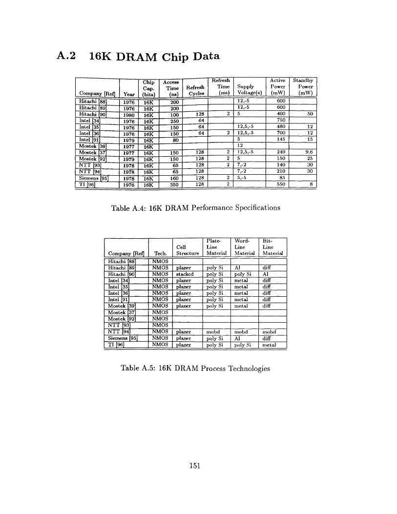
A.2 16K DRAM Chip Data
Company [Ref] YearHitachi [8) 1 1976Hitachi [891] 1976
Chip AccessCap.tv..1 I
Time Refreshn.1) Cycles
I 16K I 200-16K
RefreshTime(ns)
SupplyVoltage(s)
12,-S12,-S
ActivePower(mW)
I 600600
StandbyPower(mW)
Hitachi 90] 1980 16K 100 128 2 5 400 50
Intel 34 1976 16K 250 64 750Intel 35 1976 16K 150 64 12,5,-5 480 12Intel 36 1976 16K 150 64 2 12,5,-5 700 12Intel 91] 1979 16K 80 5 145 15
Mostek [39] 1977 16K 12
Mostek [37] 1977 16K 150 128 2 12,5,-5 240 9.6Mostek [92] 1979 16K 150 128 2 5 150 25NTT [93] 1978 16K 65 128 2 7,-2 140 30NTT [94] 1978 16K 65 128 7,-2 210 30
Siemens [95] 1978 16K 160 128 2 5,-5 85
TI[96] 1976 16K 350 128 2 550 8
Table A.4: 16K DRAM Performance Specifications
Plate- Word- Bit-Cell Line Line Line
Company [Ref] Tech. Structure Material Material Material
Hitachi [88] NMOS
Hitachi [89] NMOS planer poly Si Al diffHitachi [90] NMOS stacked poly Si poly Si AlIntel [34] NMOS planer poly Si metal diffIntel [35] NMOS planer poly Si metal diffIntel [36] NMOS planer poly Si metal diffIntel [91] NMOS planer poly Si metal diffMostek [39] NMOS planer poly Si metal diffMostek [37] NMOSMostek [92] NMOSNTT [93] NMOS
NTT [94] NMOS planer mobd mobd mobdSiemens [95] NMOS planer poly Si Al diffTI [96] NMOS planer poly Si poly Si metal
Table A.5: 16K DRAM Process Technologies
151
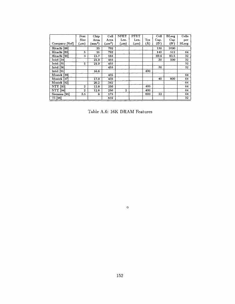
Feat Chip Cell NFET PFET Cell BLseg CellsSize Area Area Len. Len. Tox Cap. Cap per
Company [Ref] (pm) (mm 2 ) (im 2 ) (Am) (pm) (A) (fF) (fF) BLseg
Hitachi [88] 35 792 130 1690Hitachi [89] 5 35 792 140 512 64Hitachi [90] 3 15.7 184 69.6 83.5 32Intel [34] 21.9 455 30 500 32Intel [35] 5 21.9 455 32
Intel [36] 455 30 32Intel [91] 16.8 400
Mostek [39] 435 64
Mostek [37] 17.9 435 40 800 64
Mostek [92] 20.2 342 64
NTT [93] 2 12.8 256 400 64
NTT [94) 2 12.8 256 2 400 64Siemens [95] 3.5 8 175 1 600 22 1 64
TI [96) 1 632 32
Table A.6: 16K DRAM Features
152
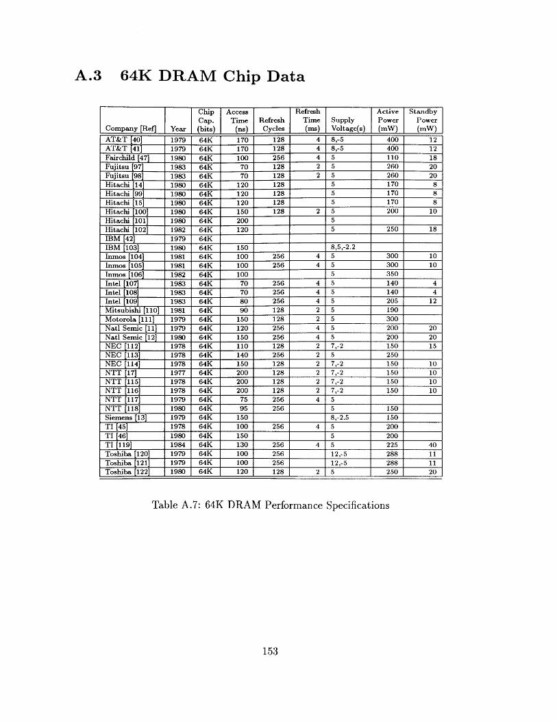
A.3 64K DRAM Chip Data
Chip Access Refresh Active StandbyCap. Time Refresh Time Supply Power Power
Company [Ref] Year (bits) (ns) Cycles (is) Voltage(s) (mW) (mW)
AT&T [40] 1979 64K 170 128 4 8,-5 400 12AT&T [41] 1979 64K 170 128 4 8,-5 400 12Fairchild [47] 1980 64K 100 256 4 5 110 18Fujitsu [97] 1983 64K 70 128 2 5 260 20Fujitsu [98] 1983 64K 70 128 2 5 260 20Hitachi [14] 1980 64K 120 128 5 170 8Hitachi [99] 1980 64K 120 128 5 170 8Hitachi [15] 1980 64K 120 128 5 170 8
Hitachi [100] 1980 64K 150 128 2 5 200 10Hitachi [101] 1980 64K 200 5
Hitachi [102] 1982 64K 120 5 250 18
IBM [42] 1979 64K
IBM [103] 1980 64K 150 8,5,-2.2
Inmos [104] 1981 64K 100 256 4 5 300 10Inmos [105] 1981 64K 100 256 4 5 300 10Inmos [106] 1982 64K 100 5 350
Intel [107] 1983 64K 70 256 4 5 140 4Intel [108] 1983 64K 70 256 4 5 140 4Intel [109] 1983 64K 80 256 4 5 205 12Mitsubishi [110] 1981 64K 90 128 2 5 190Motorola [111] 1979 64K 150 128 2 5 300Natl Semic [11] 1979 64K 120 256 4 5 200 20Natl Semic [12] 1980 64K 150 256 4 5 200 20NEC [112] 1978 64K 110 128 2 7,-2 150 15NEC [113] 1978 64K 140 256 2 5 250NEC [114] 1978 64K 150 128 2 7,-2 150 10NTT [17] 1977 64K 200 128 2 7,-2 150 10NTT [115] 1978 64K 200 128 2 7,-2 150 10NTT [116] 1978 64K 200 128 2 7,-2 150 10NTT [117] 1979 64K 75 256 4 5NTT [118] 1980 64K 95 256 5 150Siemens [13] 1979 64K 150 8,-2.5 150TI [45] 1978 64K 100 256 4 5 200TI [46] 1980 64K 150 5 200TI [119] 1984 64K 130 256 4 5 225 40Toshiba [120] 1979 64K 100 256 12,-5 288 11Toshiba [121) 1979 64K 100 256 12,-5 288 11Toshiba [122] 1980 64K 120 128 2 5 250 20
Table A.7: 64K DRAM Performance Specifications
153
6L -- aQiWo -7 j

Plate- Word- Bit-Cell Line Line Line
Company (Ref] Tech. Structure Material Material Material
AT&T [40] NMOS planer poly SiAT&T (41] NMOS planer poly Si metal poly SiFairchild [47] NMOS planer poly Si poly Si metalFujitsu [97] NMOSFujitsu [98] NMOS Al diff
Hitachi [14] NMOS planer poly Si poly Si AlHitachi [99) NMOS planer poly Si poly Si AlHitachi [15] NMOS planer poly Si poly Si AlHitachi [100] NMOS AlHitachi [101] poly Si Al
Hitachi [102] NMOS
IBM [42] SAMOS planer poly Si metal diffIBM [103] NMOS planer poly Si poly Si metalInmos [104] NMOS poly Si metal
Inmos [105] NMOS
Inmos [106) NMOS planer poly Si poly Si metalIntel (107] nwCMOSp planer poly Si poly Si AlIntel [108] nwCMOSp planer poly Si poly Si AlIntel [109] NMOS planer poly Si Al diffMitsubishi [110] NMOS planer poly Si Al poly SiMotorola [111] NMOS
Natl Semic [11] NMOS planer poly Si poly Si metalNatl Semic [12) NMOS planer poly Si poly Si metalNEC [112] NMOS planer poly Si Al
NEC [113] NMOS poly Si metal
NEC [114] NMOS poly Si AlNTT [17] NMOS
NTT [115] NMOS planer poly Si poly Si mobdNTT [116] NMOS
NTT [117) NMOS planer poly Si mobd AlNTT [118] NMOS planer poly Si mobd AlSiemens [13] VMOS vmos metal diff
TI [45] NMOS planer poly Si metal diffTI [46] NMOS
TI [119] NMOS
Toshiba [120] NMOS planer poly Si Al diffToshiba (121] NMOS planer poly Si Al diffToshiba [122] NMOS
Table A.8: 64K DRAM Process Technologies
154
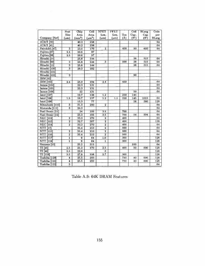
Table A.9: 64K DRAM Features
155
Feat Chip Cell NFET PFET Cell BLseg CellsSize Area Area Len. Len. Tox Cap. Cap per
Company [Ref] (pm) (mn'm2) (pm2) (gm) (pm) (A) (fF) (fF) BLseg
AT&T [40] 40.2 238 64
AT&T [41] 40.2 238 64
Fairchild [47] 3 23.5 170 2 400 50 600 64
Fujitsu [97] 2.5 19.6 97Fujitsu [98] 2.5 19.6 97 _1
Hitachi [14] 25.8 144 38 515 64
Hitachi [99] 3 25.8 144 3 500 38 515 64
Hitachi [15] 3 25.8 144 38 515 64
Hitachi [100] 3 29.3 182
Hitachi [101]
Hitachi [102] 3 90
IBM [42]
IBM [103] 2.4 25.9 194 2.4 450 64
Inmos [104] 22.3 131 64
Inmos [105] 22.3 131 64
Inmos [106] 22 131 50 64
Intel [107] 19.7 138 1.2 250 145
Intel [108] 1.5 19.7 137 1.2 1.1 250 145 1015 64Intel [109] 15.3 77 58 580 128
Mitsubishi [110] 3 31.3 200 2 64
Motorola [111] 3 24.3 64
Natl Semic [11] 24 195 3.5 700 64
Natl Semic [12] 25.3 195 3.5 1 700 54 594 64
NEC [112] 2 33.3 270 2 400 64
NEC [113] 2 32.7 307 2 400 128NEC [114] 2 33.3 270 2 400 64
NTT [17] 35.4 210 2 500 64
NTT [115] 2 35.4 210 2 500 64
NTT [116] 2 35.4 210 2 500 64
NTT [117] 1 9 64 1.0 300 128
NTT [118] 1 9 64 1 300 128
Siemens [13] 25.2 215 100 64
TI [45) 2.5 21.3 170 2.5 400 50 600 128
TI [46] 2.5 22.6 3 128
TI [119] 3.5 27.8 158 2.7 300 128
Toshiba [120] 4 25.5 200 750 40 600 128
Toshiba [121] 4 25.5 200 750 40 600 128
Toshiba [122] 3 1 1 64
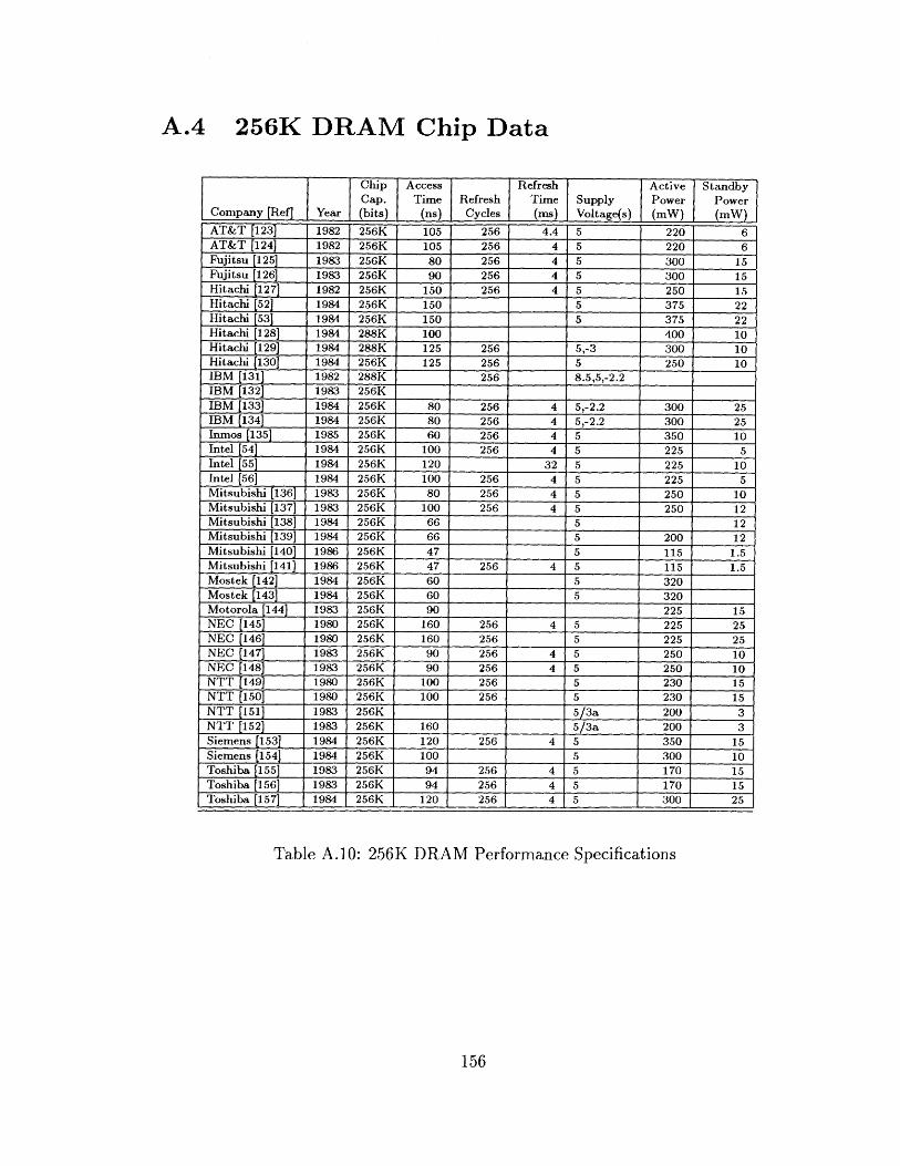
A.4 256K DRAM Chip Data
Table A.10: 256K DRAM Performance Specifications
156
Chip Access Refresh Active StandbyCap. Time Refresh Time Supply Power Power
Company [Ref] Year (bits) (ns) Cycles (ms) Voltage(s) (mW) (mW)AT&T [123] 1982 256K 105 256 4.4 5 220 6AT&T [124] 1982 256K 105 256 4 5 220 6Fujitsu (125] 1983 256K 80 256 4 5 300 15Fujitsu [126] 1983 256K 90 256 4 5 300 15Hitachi [127] 1982 256K 150 256 4 5 250 15Hitachi [52] 1984 256K 150 5 375 22Hitachi (53] 1984 256K 150 5 375 22Hitachi [128] 1984 288K 100 400 10Hitachi [129] 1984 288K 125 256 5,-3 300 10Hitachi [130] 1984 256K 125 256 5 250 10IBM [131] 1982 288K 256 8.5,5,-2.2
IBM [132] 1983 256K
IBM [133] 1984 256K 80 256 4 5,-2.2 300 25IBM [134] 1984 256K 80 256 4 5,-2.2 300 25Inmos [135] 1985 256K 60 256 4 5 350 10Intel [54) 1984 256K 100 256 4 5 225 5Intel [55] 1984 256K 120 32 5 225 10Intel (56] 1984 256K 100 256 4 5 225 5Mitsubishi [136] 1983 256K 80 256 4 5 250 10Mitsubishi [137] 1983 256K 100 256 4 5 250 12Mitsubishi [138] 1984 256K 66 5 12Mitsubishi (139] 1984 256K 66 5 200 12Mitsubishi [140] 1986 256K 47 5 115 1.5Mitsubishi [141] 1986 256K 47 256 4 5 115 1.5Mostek (142] 1984 256K 60 5 320Mostek [143] 1984 256K 60 5 320Motorola [144) 1983 256K 90 225 15NEC [145] 1980 256K 160 256 4 5 225 25NEC [146] 1980 256K 160 256 5 225 25NEC [147] 1983 256K 90 256 4 5 250 10NEC [148] 1983 256K 90 256 4 5 250 10NTT [149] 1980 256K 100 256 5 230 15NTT (150] 1980 256K 100 256 5 230 15NTT [151] 1983 256K 5/3a 200 3NTT [152) 1983 256K 160 5/3a 200 3Siemens [153] 1984 256K 120 256 4 5 350 15Siemens (154] 1984 256K 100 5 300 10Toshiba [155] 1983 256K 94 256 4 5 170 15Toshiba [156] 1983 256K 94 256 4 5 170 15Toshiba [157] 1984 256K 120 256 4 5 300 25
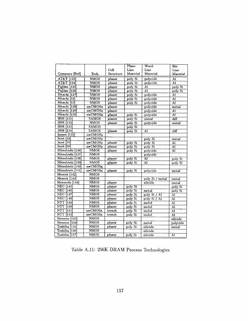
Plate- Word- Bit-Cell Line Line Line
Company [Ref] Tech. Structure Material Material Material
AT&T [123] NMOS planer poly Si polycide AlAT&T [124] NMOS planer poly Si polycide AlFujitsu [125] NMOS planer poly Si Al poly SiFujitsu [126] NMOS planer poly Si Al poly SiHitachi [127] NMOS planer poly Si polycide AlHitachi [52] NMOS planer poly Si polycide AlHitachi [53] NMOS planer poly Si polycide AlHitachi [128] nwCMOSn planer polycide metalHitachi [129] nwCMOSn planer polycide AlHitachi [130] nwCMOSn planer poly Si polycide AlIBM [131] SAMOS planer poly Si metal diffIBM [132] NMOS planer poly Si polycide metalIBM [133] SAMOS poly SiIBM [134] SAMOS planer poly Si Al diffInmos [135] nwCMOSn
Intel [54] nwCMOSp poly Si metalIntel [55] nwCMOSp planer poly Si poly Si AlIntel [56] nwCMOSp planer poly Si poly Si AlMitsubishi [136] NMOS planer poly Si polycide AlMitsubishi [137] NMOS polycideMitsubishi [138] NMOS planer poly Si Al poly SiMitsubishi [139] NMOS planer poly Si Al poly SiMitsubishi [140] nwCMOSnMitsubishi [141] nwCMOSn planer poly Si polycide metalMostek [142] NMOS
Mostek [143] NMOS poly Si / metal metalMotorola [144] NMOS planer silicide metalNEC [145] NMOS planer poly Si poly SiNEC [146] NMOS planer poly Si metal poly SiNEC [147] NMOS planer poly Si poly Si / Al AlNEC [148] NMOS planer poly Si poly Si / Al AlNTT [149] NMOS planer poly Si mobd AlNTT [150] NMOS planer poly Si mobd AlNTT [151] nwCMOSn trench poly Si mobd AlNTT [152] nwCMOSn trench poly Si mobd AlSiemens [153] NMOS silicideSiemens [154] NMOS planer poly Si metal polycideToshiba [155] NMOS planer poly Si silicide metalToshiba [156] NMOS silicideToshiba [157] NMOS planer poly Si silicide Al
Table A.11: 256K DRAM Process Technologies
157
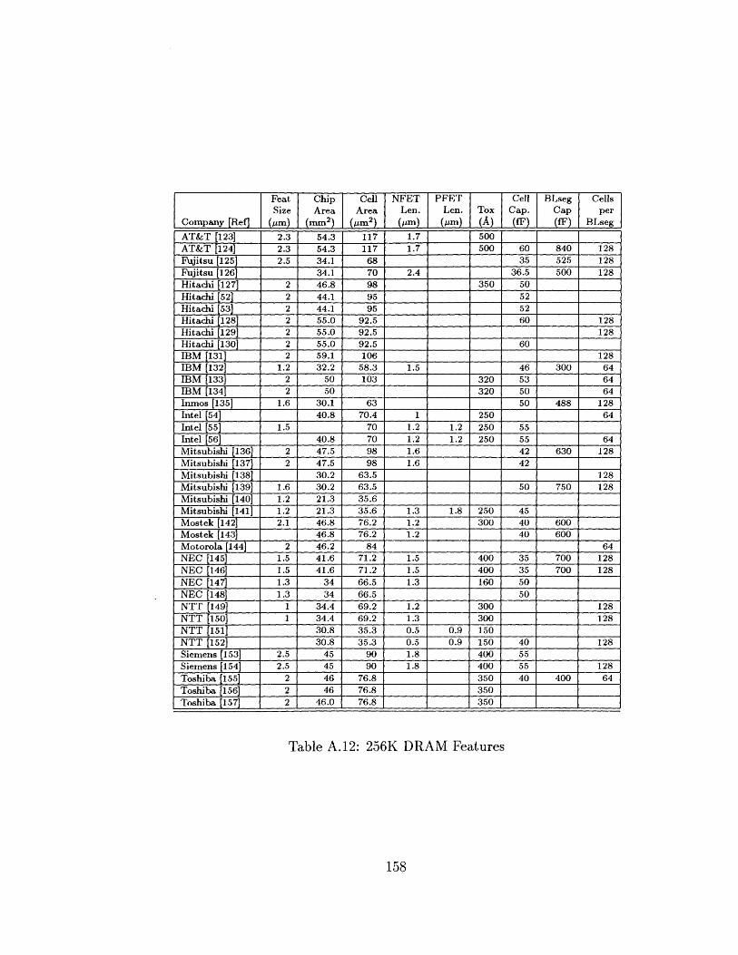
Feat Chip Cell NFET PFET Cell BLseg CellsSize Area Area Len. Len. Tox Cap. Cap per
Company [Ref] (pm) (mm2 ) (jtm 2 ) (mm) (mm) (1) (fF) (fF) BLseg
AT&T [123] 2.3 54.3 117 1.7 500
AT&T [124] 2.3 54.3 117 1.7 500 60 840 128Fujitsu [125] 2.5 34.1 68 35 525 128
Fujitsu [126] 34.1 70 2.4 36.5 500 128Hitachi [127] 2 46.8 98 350 50
Hitachi [52] 2 44.1 95 52
Hitachi [53] 2 44.1 95 52
Hitachi [128] 2 55.0 92.5 60 128
Hitachi [129] 2 55.0 92.5 1 128
Hitachi [130] 2 55.0 92.5 60IBM [131] 2 59.1 106 128
IBM [132] 1.2 32.2 58.3 1.5 46 300 64
IBM [133] 2 50 103 320 53 64
IBM [134] 2 50 320 50 64
Inmos [135] 1.6 30.1 63 50 488 128
Intel [54] 40.8 70.4 1 250 64
Intel [55) 1.5 70 1.2 1.2 250 55
Intel [56] 40.8 70 1.2 1.2 250 55 64Mitsubishi (136] 2 47.5 98 1.6 42 630 128
Mitsubishi [137] 2 47.5 98 1.6 42
Mitsubishi [138] 30.2 63.5 1 128
Mitsubishi [139] 1.6 30.2 63.5 50 750 128
Mitsubishi [140] 1.2 21.3 35.6
Mitsubishi [141] 1.2 21.3 35.6 1.3 1.8 250 45Mostek (142] 2.1 46.8 76.2 1.2 300 40 600
Mostek [143] 46.8 76.2 1.2 40 600Motorola [144] 2 46.2 84 64
NEC [145] 1.5 41.6 71.2 1.5 400 35 700 128NEC [146] 1.5 41.6 71.2 1.5 400 35 700 128NEC [147] 1.3 34 66.5 1.3 160 50NEC [148] 1.3 34 66.5 50
NTT [149] 1 34.4 69.2 1.2 300 128NTT [150] 1 34.4 69.2 1.3 300 128NTT [151] 30.8 35.3 0.5 0.9 150NTT [152] 30.8 35.3 0.5 0.9 150 40 128Siemens [153] 2.5 45 90 1.8 400 55Siemens [154) 2.5 45 90 1.8 400 55 128Toshiba [155] 2 46 76.8 350 40 400 64Toshiba [156] 2 46 76.8 350Toshiba [157] 2 46.0 76.8 350
Table A.12: 256K DRAM Features
158

A.5 1M DRAM Chip Data
Table A.13: IM DRAM Performance Specifications
159
Chip Access Refresh Active StandbyCap. Time Refresh Time Supply Power Power
Company [Ref] Year (bits) (ns) Cycles (ms) Voltage(s) (mW) (mW)AT&T [158] 1985 1M 80 512 8.8 5 160 0.5Fujitsu [159] 1985 1M 90 512 8 5 350 15Hitachi [160] 1987 1M 35 512 8 5/4i 450 30Hitachi [161] 1987 1M 32 512 8 5/4i 450Hitachi [162] 1984 1M 90 512 8 5 300 10Hitachi [163] 1984 1M 90 512 8 5 300 10Hitachi [164] 1985 1M 74 512 8 5 230 7Hitachi [165] 1986 1M 100 512 8 5 250 10IBM [166] 1984 1M 150 256 5IBM [167] 1985 1M 80 512 4 5 625 50IBM [168] 1985 1M 80 512 4 5 625 50IBM [169] 1989 IM 27 1024 8 5 450 20IBM [170] 1989 1M 27 1024 8 5 500Intel [171] 1986 1M 65 8 5 0.25Matsushita [172] 1986 1M 512 2 5Mitsubishi [173] 1985 1M 90 512 8 5 350 15Mitsubishi [174] 1985 1M 90 512 8 5 350 15Mitsubishi [175] 1987 1M 62 512 8 5 240 4Mitsubishi [176] 1990 1M 80
Mostek [177] 1985 1M 512 8 5Mostek [178] 1985 1M 85 512 8 5 225 2.5NEC [179] 1984 1M 120 256 4 5 290 15NEC [180] 1984 iM 120 256 4 5 290NEC [181] 1985 1M 85 5
NTT [182] 1984 1M 140 5 250 5
NTT [183] 1984 1M 140 512 8 5 250 5TI [62] 1986 1M 5
TI [61] 1986 1M 512 8 5 225 4Toshiba [184] 1985 1M 70 512 8 5 270 15Toshiba [185] 1986 1M 512 8 5 270 15
Toshiba [60] 1985 1M 56 512 8 5 300 15Toshiba [58] 1985 1M 56 512 8 5 150 3.5Toshiba [59] 1985 1M 56 512 8 5 150 1.0Toshiba [186] 1986 1M 56 5 175 0.25Toshiba [187] 1986 1M 56 5 175 0.25
Toshiba [188] 1986 1M 62 5 105 0.15Toshiba [189] 1986 1M 62 105 2
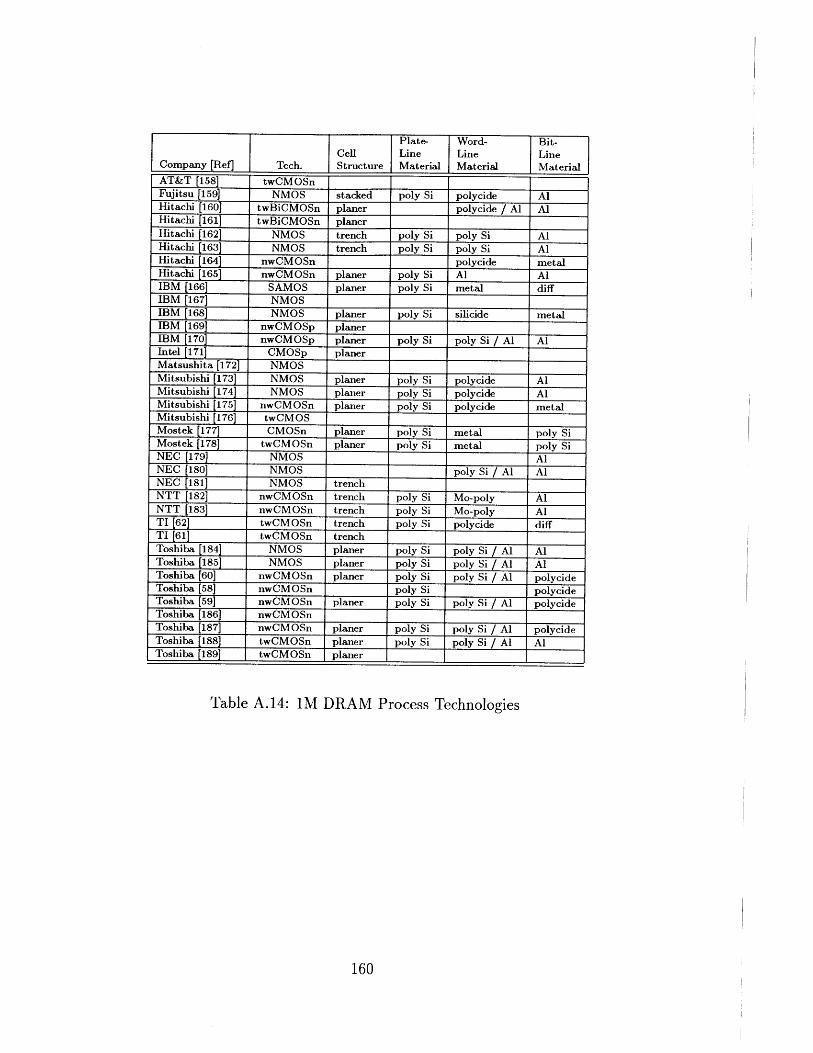
Plate- Word- Bit-Cell Line Line Line
Company [Ref] Tech. Structure Material Material MaterialAT&T [158] twCMOSn |
Fujitsu [159] NMOS stacked poly Si polycide AlHitachi [1601 twBiCMOSn planer polycide / Al AlHitachi [161] twBiCMOSn planerHitachi [162 NMOS trench poly Si poly Si AlHitachi [163] NMOS trench poly Si poly Si AlHitachi [164] nwCMOSn polycide metalHitachi [165] nwCMOSn planer poly Si Al AlIBM [166] SAMOS planer poly Si metal diffIBM [167] NMOSIBM [168] NMOS planer poly Si silicide metalIBM [169] nwCMOSp planerIBM [170] nwCMOSp planer poly Si poly Si / Al AlIntel [171] CMOSp planerMatsushita [172] NMOSMitsubishi [173] NMOS planer poly Si polycide AlMitsubishi [174] NMOS planer poly Si polycide AlMitsubishi [175] nwCMOSn planer poly Si polycide metalMitsubishi [176 twCMOSMostek [177] CMOSn planer poly Si metal poly SiMostek [178] twCMOSn planer poly Si metal poly SiNEC [179] NMOS AlNEC [180] NMOS poly Si / Al AlNEC [181] NMOS trenchNTT [182] nwCMOSn trench poly Si Mo-poly AlNTT [183] nwCMOSn trench poly Si Mo-poly AlTI [62] twCMOSn trench poly Si polycide diffTI [61] twCMOSn trenchToshiba [184] NMOS planer poly Si poly Si / Al AlToshiba [185] NMOS planer poly Si poly Si / Al AlToshiba [60] nwCMOSn planer poly Si poly Si / Al polycideToshiba [58] nwCMOSn poly Si polycideToshiba [59] nwCMOSn planer poly Si poly Si / Al polycideToshiba [186] nwCMOSn
Toshiba [187] nwCMOSn planer poly Si poly Si / Al polycideToshiba [188] twCMOSn planer poly Si poly Si / Al AlToshiba [189] twCMOSn planer
Table A.14: IM DRAM Process Technologies
160
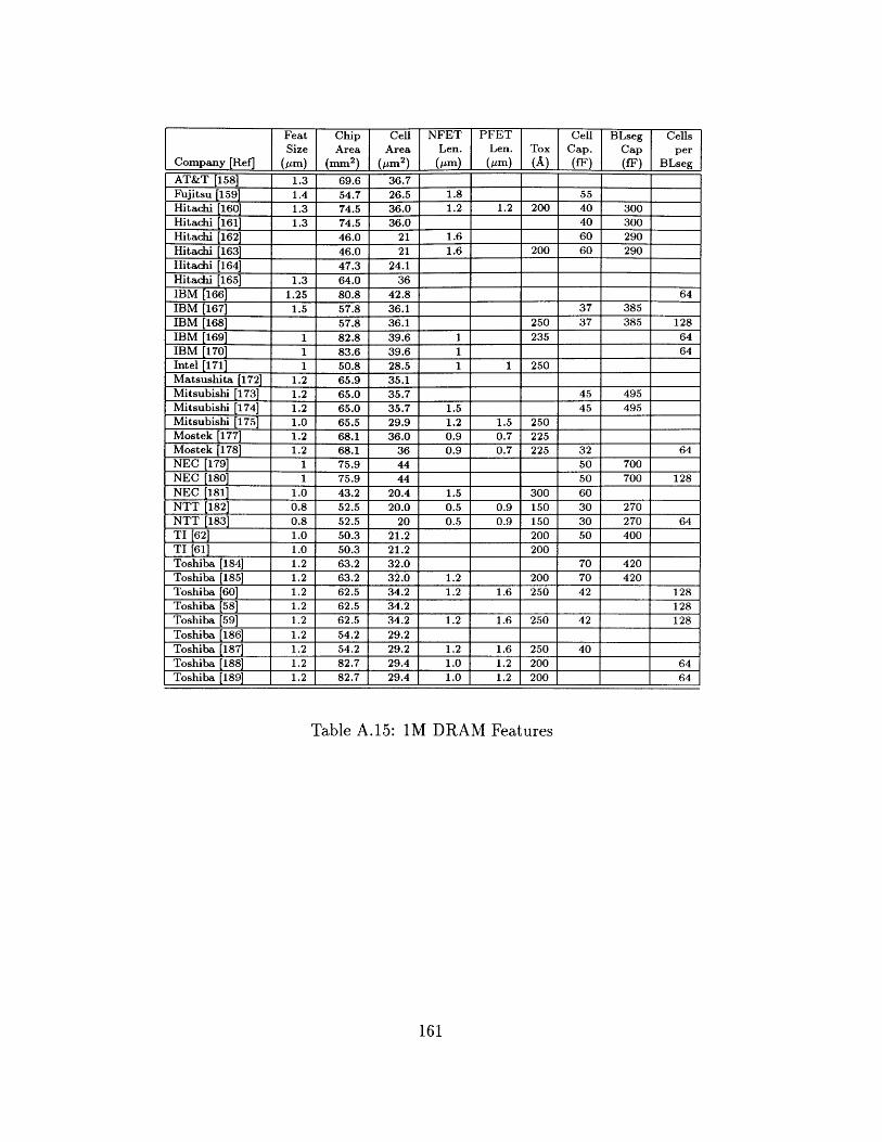
Table A.15: IM DRAM Features
161
Feat Chip Cell NFET PFET Cell BLseg CellsSize Area Area Len. Len. Tox Cap. Cap per
Company [Ref] (ym) (mm2) (pm2) (ym) (ym) (A) (fF) (fF) BLsegAT&T [158] 1.3 69.6 36.7 1Fujitsu [159] 1.4 54.7 26.5 1.8 55Hitachi [160) 1.3 74.5 36.0 1.2 1.2 200 40 300Hitachi [161] 1.3 74.5 36.0 40 300Hitachi [162] 46.0 21 1.6 60 290Hitachi [163] 46.0 21 1.6 200 60 290Hitachi [164] 47.3 24.1Hitachi [165] 1.3 64.0 36
IBM [166] 1.25 80.8 42.8 64
IBM [167] 1.5 57.8 36.1 37 385
IBM [168] 57.8 36.1 250 37 385 128IBM [169] 1 82.8 39.6 1 235 64
IBM [170] 1 83.6 39.6 1 64Intel [171] 1 50.8 28.5 1 1 250Matsushita [172] 1.2 65.9 35.1Mitsubishi [173] 1.2 65.0 35.7 45 495Mitsubishi [174] 1.2 65.0 35.7 1.5 45 495Mitsubishi [175] 1.0 65.5 29.9 1.2 1.5 250Mostek [177] 1.2 68.1 36.0 0.9 0.7 225Mostek [178] 1.2 68.1 36 0.9 0.7 225 32 64NEC [179] 1 75.9 44 50 700NEC [180] 1 75.9 44 50 700 128NEC [181] 1.0 43.2 20.4 1.5 300 60NTT [182] 0.8 52.5 20.0 0.5 0.9 150 30 270NTT [183] 0.8 52.5 20 0.5 0.9 150 30 270 64TI [62] 1.0 50.3 21.2 200 50 400TI [61] 1.0 50.3 21.2 200 1
Toshiba [184] 1.2 63.2 32.0 70 420Toshiba [185] 1.2 63.2 32.0 1.2 200 70 420Toshiba [60] 1.2 62.5 34.2 1.2 1.6 250 42 128Toshiba [58] 1.2 62.5 34.2 1 1 128Toshiba [59] 1.2 62.5 34.2 1.2 1.6 250 42 128Toshiba [186] 1.2 54.2 29.2
Toshiba [187] 1.2 54.2 29.2 1.2 1.6 250 40
Toshiba [188) 1.2 82.7 29.4 1.0 1.2 200 64Toshiba [189] 1.2 82.7 29.4 1.0 1.2 200 1 64
TA.6 4M DRAM Chip Data
Chip Access Refresh Active StandbyCap. Time Refresh Time Supply Power Power
Company [Ref] Year (bits) (ns) Cycles (ms) Voltage(s) (mW) (mW)Fujitsu [190] 1987 4M 70 1024 16 5 200 4.5Fujitsu [191] 1990 4M 5 780Hitachi [192] 1987 4M 76 1024 16 5 225 0.5Hitachi [193] 1987 4M 65 1024 5 225 0.5Hitachi [194] 1987 4M 65 1024 5 225 0.5IBM [195] 1987 4M 65 3.3 363 6.6Matsushita [196] 1987 4MMatsushita [197] 1987 4M 60 1024 5 250 3Matsushita [198] 1988 4M 70 256 16 5/3i 400 15Mitsubishi [199] 1987 4M 90 1024 5 300 2.5Mitsubishi [200] 1987 4M 90 1024 5 300Mitsubishi [201] 1990 4M 38 4096 256 5 350 1.0NEC [202] 1986 4M 95 1024 16 5/4a 425 15NEC [203] 1986 4M 95 1024 5/4a 425 15Oki [204] 1987 4M 60 5 325 5Siemens [205] 1988 4M 60 1024 16 5 350 5TI [206] 1986 4M 170 5 500 40TI [207] 1986 4M 150 5 375 10Toshiba [63] 1986 4M 80 1024 5/3.5i 300 2.5Toshiba [64] 1986 4M 80 1024 5/3.5i 300 2.5Toshiba [208] 1987 4M 60 1024 16 5 250 1.0Toshiba [209] 1987 4M 60 1024 16 5 250 1.0
Table A.16: 4M DRAM Performance Specifications
162

Plate- Word- Bit-Cell Line Line Line
Company [Ref] Tech. Structure Material Material Material
Fujitsu [190] nwCMOSn stacked poly Si poly Si / metal polycideFujitsu [191] nwCMOS stacked
Hitachi [192] twCMOS stacked poly Si poly Si AlHitachi [193] twCMOSn stacked
Hitachi [194] twCMOSn
IBM [195] nwCMOSp trench sub silicideMatsushita [196] twCMOS trench
Matsushita [197] twCMOSn trench poly Si poly Si Al polycideMatsushita [198] CMOSn trench poly Si polycide AlMitsubishi [199] twCMOSn trench poly Si polycide / Al polycideMitsubishi [200] twCMOSn trench poly Si polycide / Al polycideMitsubishi [201] twCMOS stacked
NEC [202] NMOS trench sub polycide AlNEC [203] NMOS trench sub polycide AlOki [204] nwCMOS trench
Siemens [205] CMOS trench poly Si
TI [206] twCMOSn trench sub poly Si / metal diffTI [207] twCMOSn trench sub poly Si / metal diffToshiba [63] twCMOSn trench
Toshiba [64] twCMOSn trench poly Si poly Si / Al polycideToshiba [208] twCMOSn trench
Toshiba [209] twCMOSn trench poly Si poly Si / Al polycide
Table A.17: 4M DRAM Process Technologies
163

Feat Chip Cell NFET PFET Cell BLseg CellsSize Area Area Len. Len. Tox Cap. Cap per
Company [Ref] (pim) (mm2) (pUm2) (pm) (pm) (A) (fF) (fF) BLseg
Fujitsu [190] 0.7 63.7 7.5
Hitachi [192] 0.8 111 14.7
Hitachi [193] 0.8 111 14.7 1.2
Hitachi [194] 0.8 111 14.7
IBM [195] 0.8 78 11 1
Matsushita [196] 0.8 95.6 10.1 1 -- 90 128
Matsushita [197] 0.8 67.1 8.0 0.8 1.1 170 40 256
Matsushita [198] 0.8 95.6 10.1 90 128
Mitsubishi [199] 0.8 72.3 10.9 50
Mitsubishi [200] 0.8 72.3 10.9 50 128
NEC [202] 0.8 99.2 10.6 50 400
NEC [203] 0.8 99.2 10.6 1.0 50 400 128
Oki [204] 1 149 16.8 40
Siemens [205] 0.9 91.3 10.6 0.75 0.60 200 128
TI [206] 1 100 8.8 1.0 1.0
TI [207] 1 100 8.8 1.0 1.0 64
Toshiba [63] 1.0 137 17.4 1.0 1.4 1 40
Toshiba [64] 1 137 17.4 1.0 1.4 200 40 600
Toshiba [208] 0.9 111 13.8
Toshiba [209] 0.9 111 13.8 1.0 1.2
Table A.18: 4M DRAM Features
164

A.7 16M DRAM Chip Data
Chip Access Refresh Active StandbyCap. Time Refresh Time Supply Power Power
Company [Ref] Year (bits) (ns) Cycles (ms) Voltage(s) (mW) (mW)Hitachi [70] 1988 16M 60 2048 5/3.3a 420 15Hitachi [68] 1988 16M 60 2048 5/3.3a 420 15IBM [210], [211] 1990 16M 50 2048 5or3/?iMatsushita [212] 1988 16M 65 5/4i/3a 450 5Matsushita [213] 1988 16M 65 5/4i/3a 450 5Mitsubishi [71] 1989 16M 60 2048 32 3.3 297 0.66Mitsubishi [72] 1989 16M 60 2048 32 3.3 297 0.66NEC [214] 1989 16M 55 2048 32 5/3.3a 400 10NTT [74] 1987 16M 80 3.3 500Oki [73] 1989 16M 60 2048 32 5/4i 425 2.5Samsung [215] 1989 16M 65 2048 32 5/4i 400 5Samsung [216] 1989 16M 65 2048 32 5/4i 400 5Toshiba [217] 1988 16M 70 2048 32 5/4i 600Toshiba [218] 1989 16M 70 2048 32 5/4i 600Toshiba [76] 1989 16M 45 5/4i 325 2.5Toshiba [77 1989 16M 45 5/4i 325 2.5
Table A.19: 16M DRAM Performance Specifications
Table A.20: 16M DRAM Process Technologies
165
Plate- Word- Bit-Cell Line Line Line
Company [Ref) Tech. Structure Material Material MaterialHitachi [70] twCMOS stackedHitachi [68] twCMOS stacked poly Si / Al silicideIBM [210], [219] CMOS trench sub polycide metalMatsushita [212] nwCMOSn trench poly Si poly Si / Al polycideMatsushita [213] nwCMOSn trench poly Si poly Si / Al polycideMitsubishi [71] twCMOSn stacked poly Si polycide / Al tungstenMitsubishi [72] twCMOSn stacked poly Si polycide / Al tungstenNEC [214] CMOSn stackedNTT [74] nwCMOSn trench poly Si / Al silicideOki [73] twCMOSn trench polycideSamsung [215] twCMOSn stackedSamsung [216] twCMOSn stacked poly SiToshiba [217 twCMOSn trenchToshiba [218 twCMOSn trench poly Si poly Si / Al polycideToshiba [76] twCMOSn trenchToshiba [77] twCMOSn trench poly Si poly Si / Al poly Si
Table A.21: 16M DRAM Features
166
Feat Chip Cell NFET PFET Cell BLseg CellsSize Area Area Len. Len. Tox Cap. Cap per
Company [Ref] (pm) (mm2) (pm2) (tim) (pm) (A) (fF) (fF) BLseg
Hitachi [70] 0.6 142 4.16 33Hitachi [68] 0.6 142 4.16 0.6 0.9 150 33 300IBM [210] 0.5 141 4.13 100 322 256Matsushita [212] 0.5 93.8 3.3 0.4 0.7 100 50 256Matsushita [213 0.5 93.8 3.3 0.4 0.7 100 63 380 256Mitsubishi [71] 0.5 135 4.8 0.6 0.8 128Mitsubishi [72] 0.5 135 4.8 0.6 0.8 35 210 128NEC [214] 0.55 130 4.05NTT [74] 0.7 148 4.88 0.5 0.7 120 70 420Oki [73] 0.55 128 4.06 0.8 1.1 160 30 270 128Samsung [215] 0.6 157 5.59 30Samsung [216] 0.6 157 5.59 0.8 1.0 160 30 300 128Toshiba [217] 0.7 210 6.12 0.5 0.5 30Toshiba [218] 0.7 210 6.12 0.5 0.5 37Toshiba [76] 0.6 137 4.8 0.7 0.9Toshiba [77] 0.6 137 4.8 0.7 0.9 150 30 240 128
Appendix B
Sense Amplifier Layouts
167
GLEf Super Unleaded (89. 12. 01) task:2 Cell:LEGEND Dsn:g[1
GP M1
ND
M2
PD
crq
00
MV
N J
---
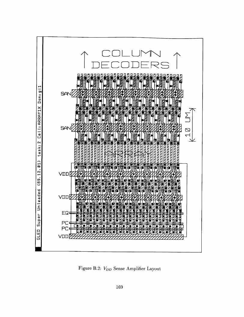
Figure B.2: VDD Sense Amplifier Layout
169
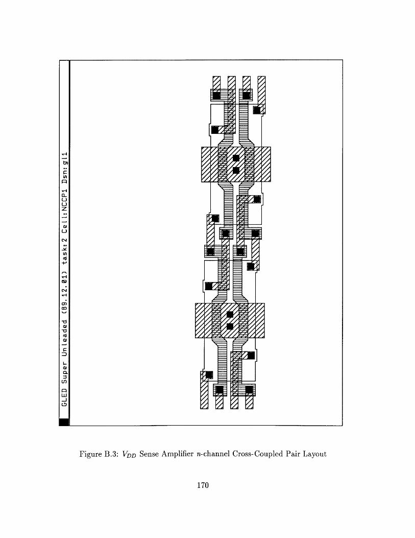
Figure B.3: VDD Sense Amplifier n-channel Cross-Coupled Pair Layout
170
i-71

I
UU
U
'3
CU
.
'-1
tn0'
cu
cJCL
Figure B.4: VDD Sense Amplifier p-channel Cross-Coupled Pair Layout
171

Figure B.5: VDD Sense Amplifier Precharge and Equalization Device Layout
172
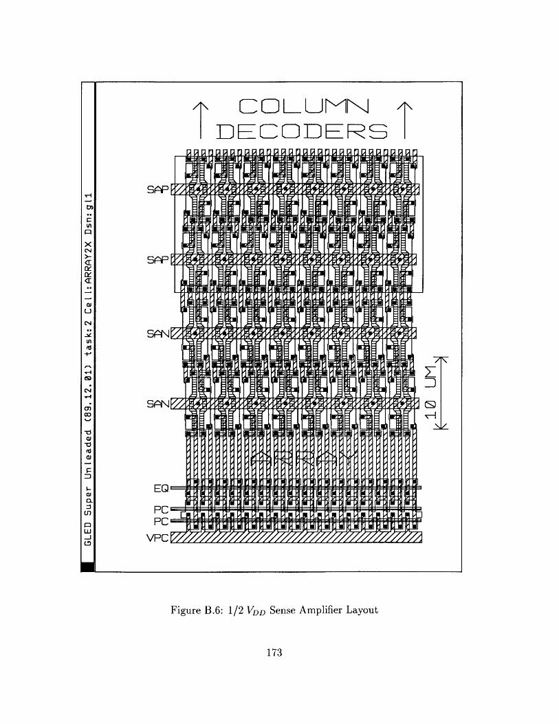
GLED Super Unleaded (89.12.01) task:2 Cetl:ARRAY2X Dsn:gl1
XN
Ii
1 uM
10FF
11
o~.
~1 CJ:
2
S ~1 p.,
C
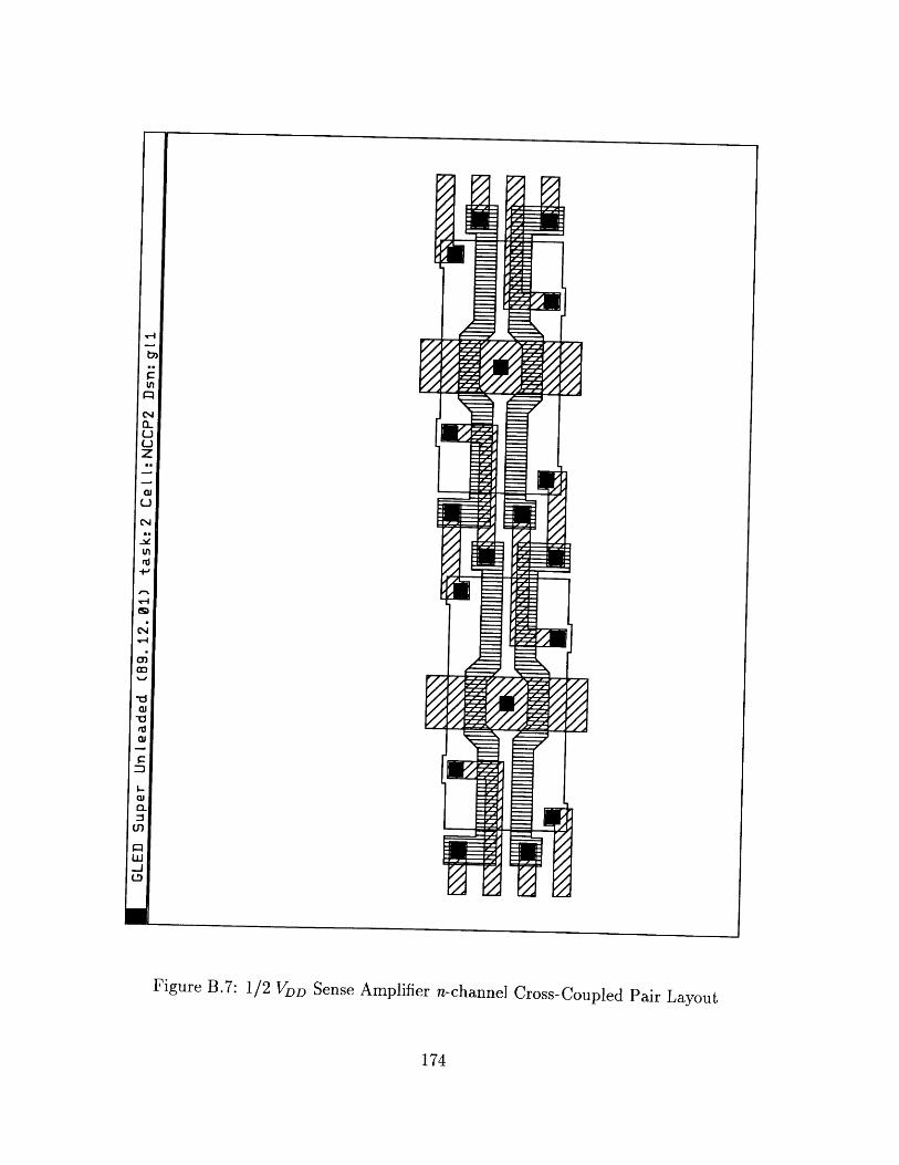
0 00 F
VAI
in
04UUz
ouU
CN
-IC,
-AoJ
cu
Figure B.7: 1/2 VDD Sense Amplifier n-channel Cross-Coupled Pair Layout
174
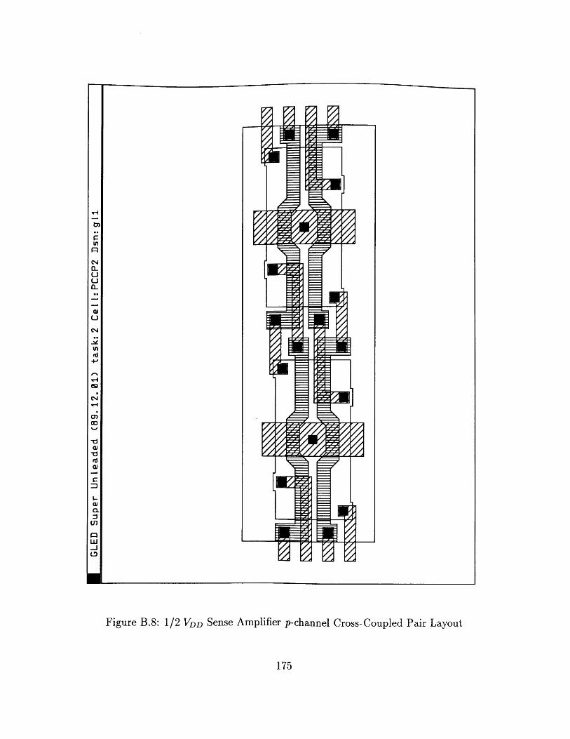
0)I
U,
U
U
'U
C-4
_d
0 1
rd-
cu.
U)
w-jC)3
Figure B.8: 1/2 VDD Sense Amplifier p-channel Cross-Coupled Pair Layout
175
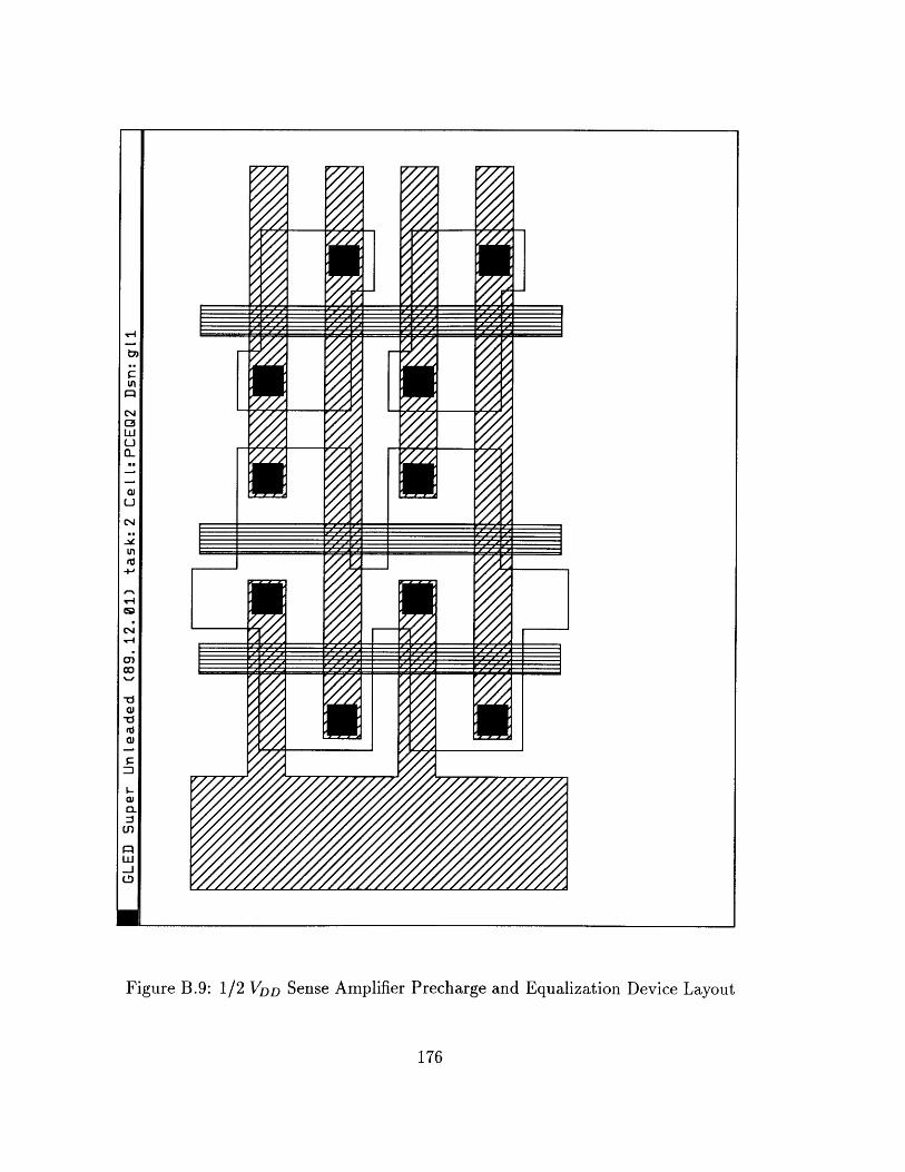
Figure B.9: 1/2 VDD Sense Amplifier Precharge and Equalization Device Layout
176
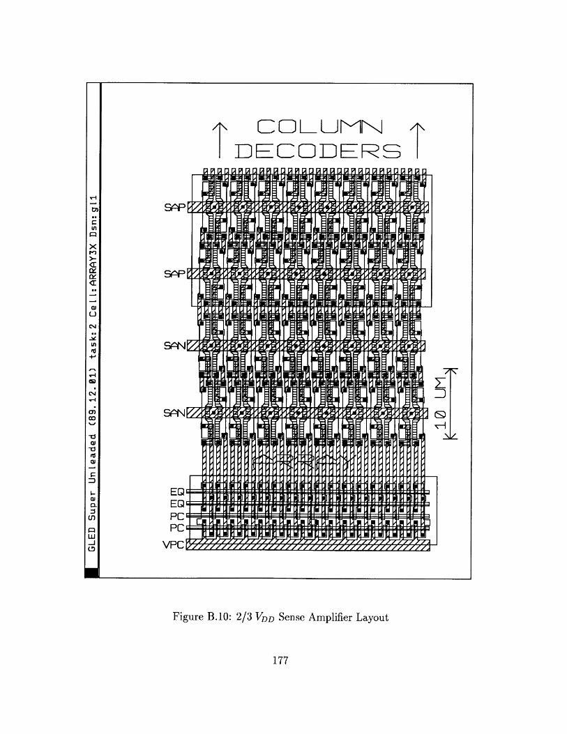
GLED Super Unleaded (89. 12.01) task:2 Ce
l:rARRAY3X
Dsn:gl1
cr2
07 LiE xZ
-- - -
--- 10
uM
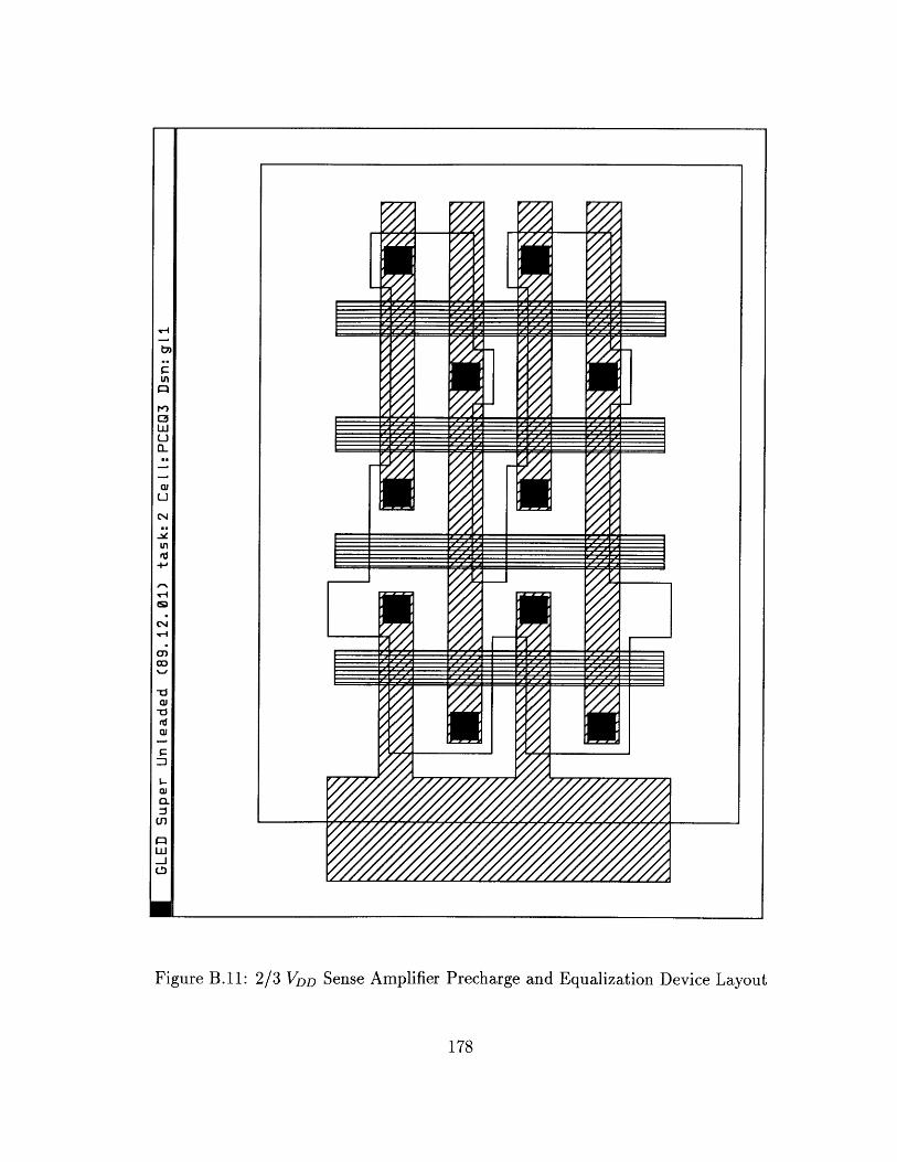
C)in
0
U
U
rd
-d
Q.
U
-ij
Figure B.11: 2/3 VDD Sense Amplifier Precharge and Equalization Device Layout
178
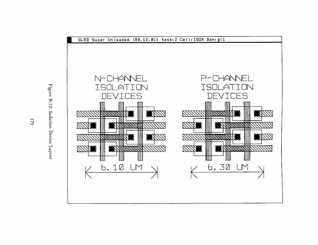
g GLED Super Unleaded (89. 12.01) task:2 Cell: ISOX Dsn:gli
N-CHANNELISOLATION
DEVICES
P-CHANNELISOLATION
DEVICES0Dl
1111 1II11
b. 10 UM If b. 30 UM NK A N A
0
I/
I-
/I