Adaptive-Latency DRAM: Optimizing DRAM Timing...
13
Adaptive-Latency DRAM: Optimizing DRAM Timing for the Common-Case Donghyuk Lee Yoongu Kim Gennady Pekhimenko Samira Khan Vivek Seshadri Kevin Chang Onur Mutlu Carnegie Mellon University {donghyu1, yoongukim, gpekhime, samirakhan, visesh, kevincha, onur}@cmu.edu Abstract In current systems, memory accesses to a DRAM chip must obey a set of minimum latency restrictions specified in the DRAM standard. Such timing parameters exist to guarantee re- liable operation. When deciding the timing parameters, DRAM manufacturers incorporate a very large margin as a provision against two worst-case scenarios. First, due to process varia- tion, some outlier chips are much slower than others and can- not be operated as fast. Second, chips become slower at higher temperatures, and all chips need to operate reliably at the high- est supported (i.e., worst-case) DRAM temperature (85 ◦ C). In this paper, we show that typical DRAM chips operating at typ- ical temperatures (e.g., 55 ◦ C) are capable of providing a much smaller access latency, but are nevertheless forced to operate at the largest latency of the worst-case. Our goal in this paper is to exploit the extra margin that is built into the DRAM timing parameters to improve perfor- mance. Using an FPGA-based testing platform, we first char- acterize the extra margin for 115 DRAM modules from three major manufacturers. Our results demonstrate that it is possi- ble to reduce four of the most critical timing parameters by a minimum/maximum of 17.3%/54.8% at 55 ◦ C without sac- rificing correctness. Based on this characterization, we pro- pose Adaptive-Latency DRAM (AL-DRAM), a mechanism that adaptively reduces the timing parameters for DRAM modules based on the current operating condition. AL-DRAM does not require any changes to the DRAM chip or its interface. We evaluate AL-DRAM on a real system that allows us to re- configure the timing parameters at runtime. We show that AL- DRAM improves the performance of memory-intensive work- loads by an average of 14% without introducing any errors. We discuss and show why AL-DRAM does not compromise re- liability. We conclude that dynamically optimizing the DRAM timing parameters can reliably improve system performance. 1. Introduction A DRAM chip is made of capacitor-based cells that represent data in the form of electrical charge. To store data in a cell, charge is injected, whereas to retrieve data from a cell, charge is extracted. Such movement of charge is not only the center- piece of DRAM operation, but also the bottleneck of DRAM latency [36, 66]. This is due to two fundamental reasons. First, when injecting charge into a cell, a wire called the bitline — through which the charge is delivered — impedes the flow of charge [36, 66]. Owing to the large resistance and the large ca- pacitance of the bitline, the cell experiences a large RC-delay, which increases the time it takes for the cell to become fully charged. Second, when extracting charge from a cell, the cell is incapable of mobilizing a strong flow of charge out of itself and into the bitline [36, 66]. Limited by the finite amount of charge stored in its small capacitor, the cell has an inherently weak charge-drive, which is further weakened as the cell loses more of its charge to the bitline. As a result, the cell cannot charge the bitline quickly (or even fully). When a DRAM chip is accessed, it requires a certain amount of time before enough charge can move into the cell (or the bitline) for the data to be reliably stored (or retrieved). To guarantee this behavior, DRAM manufacturers impose a set of minimum latency restrictions on DRAM accesses, called tim- ing parameters [25]. Ideally, timing parameters should pro- vide just enough time for a DRAM chip to operate correctly. In practice, however, DRAM manufacturers pessimistically in- corporate a very large margin into their timing parameters to ensure correct operation under worst-case conditions. This is because of two major concerns. First, due to process varia- tion, some outlier cells suffer from a larger RC-delay than other cells, and require more time to be charged. For example, an outlier cell could have a very narrow connection (i.e., contact) to the bitline, which constricts the flow of charge and increases the RC-delay [37]. Second, due to temperature dependence, all cells suffer from a weaker charge-drive at high tempera- tures, and require more time to charge the bitline. DRAM cells are intrinsically leaky, and lose some of their charge even when they are not being accessed. At high temperatures, this leakage is accelerated exponentially [29, 41, 48, 57, 74], leaving a cell with less charge to drive the bitline when the cell is accessed — increasing the time it takes for the bitline to be charged. Consequently, timing parameters prescribed by the DRAM manufacturers are dictated by the worst-case cells (the slow- est cells) operating under the worst-case conditions (the high- est temperature of 85 ◦ C [25]). Such pessimism on the part of the DRAM manufacturers is motivated by their desire to (i) in- crease chip yield and (ii) reduce chip testing time. The man- ufacturers, in turn, are driven by the extremely cost-sensitive nature of the DRAM market, which encourages them to adopt pessimistic timing parameters rather than to (i) discard chips with the slowest cells or (ii) test chips at lower temperatures. Ultimately, the burden of pessimism is passed on to the end- users, who are forced to endure much greater latencies than what is actually needed for reliable operation under common- case conditions. In this paper, we first characterize 115 DRAM modules from three manufacturers to expose the excessive margin that
Transcript of Adaptive-Latency DRAM: Optimizing DRAM Timing...

Adaptive-Latency DRAM: Optimizing DRAM Timing for the Common-Case
Donghyuk Lee Yoongu Kim Gennady PekhimenkoSamira Khan Vivek Seshadri Kevin Chang Onur Mutlu
Carnegie Mellon University
{donghyu1, yoongukim, gpekhime, samirakhan, visesh, kevincha, onur}@cmu.edu
AbstractIn current systems, memory accesses to a DRAM chip must
obey a set of minimum latency restrictions specified in theDRAM standard. Such timing parameters exist to guarantee re-liable operation. When deciding the timing parameters, DRAMmanufacturers incorporate a very large margin as a provisionagainst two worst-case scenarios. First, due to process varia-tion, some outlier chips are much slower than others and can-not be operated as fast. Second, chips become slower at highertemperatures, and all chips need to operate reliably at the high-est supported (i.e., worst-case) DRAM temperature (85◦C). Inthis paper, we show that typical DRAM chips operating at typ-ical temperatures (e.g., 55◦C) are capable of providing a muchsmaller access latency, but are nevertheless forced to operateat the largest latency of the worst-case.
Our goal in this paper is to exploit the extra margin thatis built into the DRAM timing parameters to improve perfor-mance. Using an FPGA-based testing platform, we first char-acterize the extra margin for 115 DRAM modules from threemajor manufacturers. Our results demonstrate that it is possi-ble to reduce four of the most critical timing parameters bya minimum/maximum of 17.3%/54.8% at 55◦C without sac-rificing correctness. Based on this characterization, we pro-pose Adaptive-Latency DRAM (AL-DRAM), a mechanism thatadaptively reduces the timing parameters for DRAM modulesbased on the current operating condition. AL-DRAM does notrequire any changes to the DRAM chip or its interface.
We evaluate AL-DRAM on a real system that allows us to re-configure the timing parameters at runtime. We show that AL-DRAM improves the performance of memory-intensive work-loads by an average of 14% without introducing any errors.We discuss and show why AL-DRAM does not compromise re-liability. We conclude that dynamically optimizing the DRAMtiming parameters can reliably improve system performance.
1. IntroductionA DRAM chip is made of capacitor-based cells that representdata in the form of electrical charge. To store data in a cell,charge is injected, whereas to retrieve data from a cell, chargeis extracted. Such movement of charge is not only the center-piece of DRAM operation, but also the bottleneck of DRAMlatency [36, 66]. This is due to two fundamental reasons. First,when injecting charge into a cell, a wire called the bitline —through which the charge is delivered — impedes the flow ofcharge [36, 66]. Owing to the large resistance and the large ca-pacitance of the bitline, the cell experiences a large RC-delay,which increases the time it takes for the cell to become fully
charged. Second, when extracting charge from a cell, the cellis incapable of mobilizing a strong flow of charge out of itselfand into the bitline [36, 66]. Limited by the finite amount ofcharge stored in its small capacitor, the cell has an inherentlyweak charge-drive, which is further weakened as the cell losesmore of its charge to the bitline. As a result, the cell cannotcharge the bitline quickly (or even fully).
When a DRAM chip is accessed, it requires a certainamount of time before enough charge can move into the cell (orthe bitline) for the data to be reliably stored (or retrieved). Toguarantee this behavior, DRAM manufacturers impose a set ofminimum latency restrictions on DRAM accesses, called tim-ing parameters [25]. Ideally, timing parameters should pro-vide just enough time for a DRAM chip to operate correctly.In practice, however, DRAM manufacturers pessimistically in-corporate a very large margin into their timing parameters toensure correct operation under worst-case conditions. This isbecause of two major concerns. First, due to process varia-tion, some outlier cells suffer from a larger RC-delay than othercells, and require more time to be charged. For example, anoutlier cell could have a very narrow connection (i.e., contact)to the bitline, which constricts the flow of charge and increasesthe RC-delay [37]. Second, due to temperature dependence,all cells suffer from a weaker charge-drive at high tempera-tures, and require more time to charge the bitline. DRAM cellsare intrinsically leaky, and lose some of their charge even whenthey are not being accessed. At high temperatures, this leakageis accelerated exponentially [29, 41, 48, 57, 74], leaving a cellwith less charge to drive the bitline when the cell is accessed— increasing the time it takes for the bitline to be charged.
Consequently, timing parameters prescribed by the DRAMmanufacturers are dictated by the worst-case cells (the slow-est cells) operating under the worst-case conditions (the high-est temperature of 85◦C [25]). Such pessimism on the part ofthe DRAM manufacturers is motivated by their desire to (i) in-crease chip yield and (ii) reduce chip testing time. The man-ufacturers, in turn, are driven by the extremely cost-sensitivenature of the DRAM market, which encourages them to adoptpessimistic timing parameters rather than to (i) discard chipswith the slowest cells or (ii) test chips at lower temperatures.Ultimately, the burden of pessimism is passed on to the end-users, who are forced to endure much greater latencies thanwhat is actually needed for reliable operation under common-case conditions.
In this paper, we first characterize 115 DRAM modulesfrom three manufacturers to expose the excessive margin that

is built into their timing parameters. Using an FPGA-basedtesting platform [29, 31, 41], we then demonstrate that DRAMtiming parameters can be shortened to reduce DRAM latencywithout sacrificing any observed degree of DRAM reliability.We are able to reduce latency by taking advantage of the twolarge gaps between the worst-case and the “common-case.”First, most DRAM chips are not exposed to the worst-case tem-perature of 85◦C: according to previous studies [11, 12, 43] andour own measurements (Section 4.2), the ambient temperaturearound a DRAM chip is typically less than 55◦C. Second, mostDRAM chips do not contain the worst-case cell with the largestlatency: the slowest cell for a typical chip is still faster than thatof the worst-case chip (Section 7).
Based on our characterization, we propose Adaptive-Latency DRAM (AL-DRAM), a mechanism that dynamicallyoptimizes the timing parameters for different modules at dif-ferent temperatures. AL-DRAM exploits the additional chargeslack present in the common-case compared to the worst-case,thereby preserving the level of reliability (at least as high as theworst-case) provided by DRAM manufacturers. We evaluateAL-DRAM on a real system [5, 6] that allows us to dynami-cally reconfigure the timing parameters at runtime. We showthat AL-DRAM improves the performance of a wide variety ofmemory-intensive workloads by 14.0% (on average) withoutintroducing errors. Therefore, we conclude that AL-DRAMimproves system performance while maintaining memory cor-rectness and without requiring changes to DRAM chips or theDRAM interface.
This paper makes the following contributions:
• We provide a detailed analysis of why we can reduceDRAM timing parameters without sacrificing reliability.We show that the latency of a DRAM access depends onhow quickly charge moves into or out of a cell. Comparedto the worst-case cell operating at the worst-case tempera-ture (85◦C), a typical cell at a typical temperature allowsmuch faster movement of charge, leading to shorter accesslatency. This enables the opportunity to reduce timing pa-rameters without introducing errors.
• Using an FPGA-based testing platform, we profile 115DRAM modules (from three manufacturers) and expose thelarge margin built into their timing parameters. In particu-lar, we identify four timing parameters that are the mostcritical during a DRAM access: tRCD, tRAS, tWR, andtRP. At 55◦C, we demonstrate that the parameters can bereduced by an average of 17.3%, 37.7%, 54.8%, and 35.2%while still maintaining correctness. For some chips, the re-ductions are as high as 27.3%, 42.8%, 66.7%, and 45.4%.
• We propose a practical mechanism, Adaptive-LatencyDRAM (AL-DRAM), to take advantage of the above obser-vation. The key idea is to dynamically adjust the DRAMtiming parameters for each module based on its latencycharacteristics and temperature so that the timing param-eters are dynamically optimized for the current operatingcondition. We show that the hardware cost of AL-DRAMis very modest, with no changes to DRAM.
• We evaluate AL-DRAM on a real system [5, 6] running real
workloads by dynamically reconfiguring the timing param-eters. For a wide variety of memory-intensive workloads,AL-DRAM improves system performance by an average of14.0% and a maximum of 20.5% without incurring errors.
2. DRAM BackgroundTo understand the dominant sources of DRAM latency, we firstprovide the necessary background on DRAM organization andoperation.
2.1. DRAM Organization
Figure 1a shows the internal organization of a DRAM subar-ray [8, 34, 36, 62], which consists of a 2-D array of DRAMcells connected to a single row of sense amplifiers (a row ofsense amplifiers is also referred to as a row buffer). The senseamplifier is a component that essentially acts as a latch — itdetects the data stored in the DRAM cell and latches on to thecorresponding data.
Figure 1b zooms in on the connection between a singleDRAM cell and its corresponding sense amplifier. Each cellconsists of (i) a capacitor that stores a bit of data in the form ofelectrical charge, and (ii) an access transistor that determineswhether the cell is connected to the sense amplifier. The senseamplifier consists of two cross-coupled inverters. The wire thatconnects the cell to the sense amplifier is called the bitline,whereas the wire that controls the access transistor is called thewordline. Figure 1c depicts a simplified view of a cell as wellas its bitline and sense amplifier, in which electrical charge isrepresented in gray. Switch À represents the access transistorcontrolled by the wordline, and switch Á represents the on/offstate of the sense amplifier.
columncell
row
wordlinesense-amplifier
(a) Subarray
capa
cito
r
ref.
bit
line
cell
wordline
accesstransistor
bitl
ine
sense-amplifier
(b) Cell
cellcapacitor
bitl
ine
sense-amplifier
parasiticcapacitor
wordline
bitline
ref. bitline
✎
�
(c) Simplified ViewFigure 1: DRAM Organization
2.2. DRAM Operation: Commands & Timing Constraints
As shown in Figure 2, a cell transitions through five differentstates during each access. In the first state Ê, which is calledthe precharged state, the cell is “fully” charged, while the bit-line is only halfway charged (i.e., the bitline voltage is main-tained at 1
2VDD ). In practice, the cell is usually not completelycharged because of a phenomenon called leakage, wherein thecell capacitor loses charge over time.
In order to access data from a cell, the DRAM controller is-sues a command called ACTIVATE. Upon receiving this com-mand, DRAM increases the wordline voltage, thereby connect-ing the cell to the bitline. Since the cell is at a higher voltagethan the bitline, the cell then drives its charge into the bitlineuntil their voltages are equalized at 1
2VDD + δ. This is depictedin state Ë, which is called charge-sharing.
Subsequently, the sense amplifier is enabled, which then
2

✌
cellcap.
bitl
ine
sense-amp.
bitlinecap.
�
Command
tRAS (35ns) tRP (13.75ns)
Activation (ACT) Read/Write (RD/WR) Precharge (PRE) tRCD (13.75ns)
Parameter
reduced charge
charge leakage
DDV2
1DDV
0
DDV4
3 DDV
DDV
✁✂DDV2
1
✄ Precharged Charge-Sharing☎ RestoredSense-Amplification
✆ Precharged
Figure 2: DRAM Operations, Commands and Parameters
senses and amplifies the difference in the bitline voltage and12VDD . During this process, referred to as sensing and ampli-fication, the sense amplifier drives the bitline voltage to VDD .Since the cell is still connected to the bitline, this process alsoinjects charge into the cell. Midway through the sense amplifi-cation process (state Ì), when the bitline reaches an intermedi-ate voltage level (e.g., 3
4VDD ), data can be read out or writteninto the bitline. This is done by issuing a READ or WRITEcommand to the corresponding cell. The time taken to reachthis state (Ì) after issuing the ACTIVATE is expressed as atiming parameter called tRCD.
After completing the sense amplification, the bitline volt-age reaches VDD and the cell charge is fully restored (state Í).The time taken to reach this state after issuing the ACTIVATEis expressed as a timing parameter called tRAS. If there is awrite operation, some additional time is required for the bitlineand the cell to reach this state, which is expressed as a timingparameter called tWR.
Before we can access data from a different cell connected tothe same bitline, the sense amplifier must be taken back to theprecharged state. This is done by issuing a PRECHARGE com-mand. Upon receiving this command, DRAM first decreasesthe wordline voltage, thereby disconnecting the cell from thebitline. Next, DRAM disables the sense amplifier and drivesthe bitline back to a voltage of 1
2VDD (state Î). The time takenfor the precharge operation is expressed as a timing parametercalled tRP.
At state Î, note that the cell is completely filled with charge.Subsequently, however, the cell slowly loses some of its chargeuntil the next access (cycling back to state Ê). The length oftime for which the cell can reliably hold its charge is called thecell’s retention time. If the cell is not accessed for a long time,it may lose enough charge to invert its stored data, resulting inan error. To avoid data corruption, DRAM refreshes the chargein all of its cells at a regular interval, called the refresh interval.
3. Charge & Latency InterdependenceAs we explained, the operation of a DRAM cell is governed bytwo important concepts: (i) the quantity of charge and (ii) thelatency it takes to move charge. These two concepts are closelyrelated to each other — one cannot be adjusted without af-fecting the other. To establish a more quantitative relation-ship between charge and latency, Figure 3 presents the voltageof a cell and its bitline as they cycle through the prechargedstate, charge-sharing state, sense-amplification state, restored
state, and back to the precharged state (Section 2).1 Thiscurve is typical in DRAM operation, as also shown in priorworks [14, 27, 36, 66]. The timeline starts with an ACTIVATEat 0 ns and ends with the completion of PRECHARGE at48.75 ns. From the figure, we identify three specific periodsin time when the voltage changes slowly: (i) start of sense-amplification (part À), (ii) end of sense-amplification (part Á),and (iii) end of precharging (part Â). Since charge is corre-lated with voltage, these three periods are when the charge alsomoves slowly. In the following, we provide three observationsexplaining why these three periods can be shortened for typicalcells at typical temperatures — offering the best opportunityfor shortening the timing parameters.
0 10 20 30 40 50Time (ns)
0.00
0.25
0.50
0.75
1.00
1.25
1.50
Volta
ge (V
)
VDD
VSS
ACT PRE
Charge-Sharing Sense-Amplification Precharge
tRCDtRPtRAS
dVBL95% charged
dVBL95% precharged
VCell
VBL
VBLref
Figure 3: Phases of DRAM Voltage Levels
Observation 1. At the start of the sense-amplification phase,the higher the bitline voltage, the quicker the sense-amplifier isjump-started. Just as the amplification phase starts, the sense-amplifier detects the bitline voltage that was increased in theprevious charge-sharing phase (by the cell donating its chargeto the bitline). The sense-amplifier then begins to inject morecharge into the bitline to increase the voltage even further —triggering a positive-feedback loop where the bitline voltageincreases more quickly as the bitline voltage becomes higher.This is shown in Figure 3 where the bitline voltage ramps upfaster and faster during the initial part of the amplificationphase. Importantly, if the bitline has a higher voltage to be-gin with (at the start of sense-amplification), then the positive-
1Using 55nm DRAM parameters [55, 69], we simulate the voltage and currentof the DRAM cells, sense-amplifiers, and bitline equalizers (for prechargingthe bitline). To be technology-independent, we model the DRAM circuitry us-ing NMOS and PMOS transistors that obey the well-known MOSFET equationfor current-voltage (SPICE) [56]. We do not model secondary effects.
3

feedback is able to set in more quickly. Such a high initialvoltage is comfortably achieved by typical cells at typical tem-peratures because they donate a large amount of charge to thebitline during the charge-sharing phase (as they have a largeamount of charge). As a result, they are able to reach statesÌ and Í (Figure 2) more quickly, creating the opportunity toshorten tRCD and tRAS.
Observation 2. At the end of the sense-amplification phase,nearly half the time (42%) is spent on injecting the last 5% ofthe charge into the cell. Thanks to the positive-feedback, themiddle part of the amplification phase (part between À and Áin Figure 3) is able to increase the bitline voltage quickly. How-ever, during the later part of amplification (part Á in Figure 3),the RC-delay becomes much more dominant, which preventsthe bitline voltage from increasing as quickly. In fact, it takesa significant amount of extra delay for the bitline voltage toreach VDD (Figure 3) that is required to fully charge the cell.However, for typical cells at typical temperatures, such an extradelay may not be needed — the cells could already be injectedwith enough charge for them to comfortably share with the bit-line when they are next accessed. This allows us to shorten thelater part of the amplification phase, creating the opportunityto shorten tRAS and tWR.
Observation 3. At the end of the precharging phase, nearlyhalf the time (45%) is spent on extracting the last 5% of thecharge from the bitline. Similar to the amplification phase, thelater part of the precharging phase is also dominated by theRC-delay, which causes the bitline voltage to decrease slowlyto 1
2VDD (part  in Figure 3). If we decide to incur less thanthe full delay required for the bitline voltage to reach exactly12VDD , it could lead to two different outcomes depending onwhich cell we access next. First, if we access the same cellagain, then the higher voltage left on the bitline works in ourfavor. This is because the cell — which is filled with charge— would have increased the bitline voltage anyway during thecharge-sharing phase. Second, if we access a different cellconnected to the same bitline, then the higher voltage left onthe bitline may work as a handicap. Specifically, this happensonly when the cell is devoid of any charge (e.g., storing a dataof ‘0’). For such a cell, its charge-sharing phase operates inthe opposite direction, where the cell steals some charge awayfrom the bitline to decrease the bitline voltage. Subsequently,the voltage is “amplified” to 0 instead of VDD . Nevertheless,typical cells at typical temperatures are capable of comfortablyovercoming the handicap — thanks to their large capacitance,the cells are able to steal a large amount of charge from thebitline. As a result, this creates the opportunity to shorten tRP.
4. Charge Gap: Common-Case vs. Worst-CaseBased on the three observations, we understand that timing pa-rameters can be shortened if the cells have enough charge. Im-portantly, we showed that such a criterion is easily satisfied fortypical cells at typical temperatures. In this section, we ex-plain what it means for a cell to be “typical” and why it hasmore charge at “typical” temperatures. Specifically, we exam-ine two physical phenomena that critically impact a DRAMcell’s ability to receive and retain charge: (i) process variationand (ii) temperature dependence.
4.1. Process Variation: Cells Are Not Created Equal
Process variation is a well-known phenomenon that introducesdeviations between a chip’s intended design and its actual im-plementation [13, 37, 60]. DRAM cells are affected by pro-cess variation in two major aspects: (i) cell capacitance and(ii) cell resistance. Although every cell is designed to have alarge capacitance (to hold more charge) and a small resistance(to facilitate the flow of charge), some deviant cells may not bemanufactured in such a manner [15, 26, 29, 30, 38, 41, 42]. InFigure 4a, we illustrate the impact of process variation usingtwo different cells: one is a typical cell conforming to design(left column) and the other is the worst-case cell deviating themost from design (right column).
As we see from Figure 4a, the worst-case cell contains lesscharge than the typical cell in state Í (Restored state, as wasshown in Figure 2). This is because of two reasons. First, dueto its large resistance, the worst-case cell cannot allow chargeto flow inside quickly. Second, due to its small capacitance,the worst-case cell cannot store much charge even when it isfull. To accommodate such a worst-case cell, existing timingparameters are set to a large value. However, worst-case cellsare relatively rare. When we analyzed 115 modules, the over-whelming majority of them had significantly more charge thanwhat is necessary for correct operation (Section 7 will providemore details).
4.2. Temperature Dependence: Hot Cells Are Leakier
Temperature dependence is a well-known phenomenon inwhich cells leak charge at almost double the rate for every 10◦Cincrease in temperature [29, 41, 48, 57, 74]. In Figure 4a, we il-lustrate the impact of temperature dependence using two cellsat two different temperatures: (i) typical temperature (55◦C,bottom row), and (ii) the worst-case temperature (85◦C, toprow) supported by DRAM standards.
As we see from the figure, both typical and worst-casecells leak charge at a faster rate at the worst-case tempera-ture. Therefore, not only does the worst-case cell have lesscharge to begin with, but it is left with even less charge be-cause it leaks charge at a faster rate (top-right in Figure 4a).To accommodate the combined effect of process variation andtemperature dependence, existing timing parameters are set toa very large value. However, most systems do not operate at85◦C [11, 12, 43].2 We measured the DRAM ambient tempera-ture in a server cluster running a memory-intensive benchmark,and found that the temperature never exceeds 34◦C — as wellas never changing by more than 0.1◦C per second. We show
2 Figure 22 in [12] and Figure 3 in [43] show that the maximum temperatureof DRAM chips at the highest CPU utilization is 60–65◦C. While some priorworks claim a maximum DRAM temperature over 80◦C [76], each DIMMin their system dissipates 15W of power. This is very aggressive nowadays— modern DIMMs typically dissipate around 2–6W (see Figure 8 of [17],2-rank configuration same as the DIMM configuration of [76]). We believethat continued voltage scaling and increased energy efficiency of DRAM havehelped reduce the DIMM power consumption. While old DDR1/DDR2 use1.8–3.0V power supplies, newer DDR3/DDR4 use only 1.2–1.5V. In addi-tion, newer DRAMs adopt more power saving techniques (i.e., temperaturecompensated self refresh, power down modes [21, 46]) that were previouslyused only by Low-Power DRAM (LPDDR). Furthermore, many previousworks [9, 39, 40, 43, 76] propose hardware/software mechanisms to maintaina low DRAM temperature and energy.
4

Rlow
largeleakage
Typical Cell
smallleakage
smallleakage
large
unfilled
leakage
(Rhigh)
Worst Cell
✌�
✌� ✌�
✌�
Rhigh
RhighRlow
unfilled(Rhigh)
Tem
pera
ture
Tem
pera
ture
Typi
cal
Wor
st
(a) Existing DRAM
largeleakage
Typical Cell
✌
smallleakage✌�
smallleakage✌�
largeleakage✌�
Tem
pera
ture
Worst Cell
Tem
pera
ture
Rlow Rhigh
RhighRlow
unfilled(Rhigh)
unfilled(Rhigh)
unfilled(by design)
unfilled(by design)
unfilled(by design)
Typi
cal
Wor
st
�
(b) Our Proposal (Adaptive-Latency DRAM)Figure 4: Effect of Reduced Latency: Typical vs. Worst (Darker Background means Less Reliable)
this in Figure 5, which plots the temperature for a 24-hour pe-riod (left) and also zooms in on a 2-hour period (right). In ad-dition, we repeated the measurement on a desktop system thatis not as well cooled as the server cluster. As Figure 6 shows,even when the CPU was utilized at 100% and the DRAM band-width was utilized at 40%, the DRAM ambient temperaturenever exceeded 50◦C. Other works [11, 12, 43] report similarresults, as explained in detail in Footnote 2. From this, we con-clude that the majority of DRAM modules are likely to operateat temperatures that are much lower than 85◦C, which slowsdown the charge leakage by an order of magnitude or morethan at the worst-case temperature.
0 4 8 12 16 20 24Time (hour)
28
29
30
31
32
33
34
Tem
pera
ture
()
4 5 6Time (hour)
28
29
30
31
32
33
34
Figure 5: DRAM Temperature in a Server Cluster
0 1 2 3 4 5 6Time (hour)
35
40
45
50
55
Tem
pera
ture
()
0
20
40
60
80
100
Utili
zatio
n (%
)
DIMM Temperature ( )CPU Utilization (%)Memory Channel Utilization (%)
Figure 6: DRAM Temperature in a Desktop System
4.3. Reliable Operation with Shortened TimingAs explained in Section 3, the amount of charge in state Ê(i.e., the precharged state in Figure 2) plays a critical role inwhether the correct data is retrieved from a cell. That is whythe worst-case condition for correctness is the top-right of Fig-ure 4a, which shows the least amount of charge stored in theworst-case cell at the worst-case temperature in state Ê. How-ever, DRAM manufacturers provide reliability guarantees evenfor such worst-case conditions. In other words, the amount ofcharge at the worst-case condition is still greater than what isrequired for correctness.
If we were to shorten the timing parameters, we would alsobe reducing the charge stored in the cells. It is important to
note, however, that we are proposing to exploit only the addi-tional slack (in terms of charge) compared to the worst-case.This allows us to provide as strong of a reliability guarantee asthe worst-case.
In Figure 4b, we illustrate the impact of shortening the tim-ing parameters in three of the four different cases: two differ-ent cells at two different temperatures. The lightened portionsinside the cells represent the amount of charge that we are giv-ing up by using the shortened timing parameters. Note thatwe are not giving up any charge for the worst-case cell at theworst-case temperature. Although the other three cells are notfully charged in state Í, when they eventually reach state Ê,they are left with a similar amount of charge as the worst-case(top-right). This is because these cells are capable of eitherholding more charge (typical cell, left column) or holding theircharge longer (typical temperature, bottom row). Therefore,optimizing the timing parameters (based on the amount of ex-isting slack) provides the opportunity to reduce overall DRAMlatency while still maintaining the reliability guarantees pro-vided by the DRAM manufacturers.
In Section 7, we present the results from our characteriza-tion study where we quantify the slack in 115 DRAM modules.Before we do so, we first propose our mechanism for identify-ing and enforcing the shortened timing parameters.
5. Adaptive-Latency DRAMOur mechanism, Adaptive-Latency DRAM (AL-DRAM), al-lows the memory controller to exploit the latency variationacross DRAM modules (DIMMs) at different operating tem-peratures by using customized (aggressive) timing parame-ters for each DIMM/temperature combination. Our mecha-nism consists of two steps: (i) identification of the best tim-ing parameters for each DIMM/temperature, and (ii) enforce-ment, wherein the memory controller dynamically extractseach DIMM’s operating temperature and uses the best timingparameters for each DIMM/temperature combination.
5.1. Identifying the Best Timing Parameters
Identifying the best timing parameters for each DIMM at dif-ferent temperatures is the more challenging of the two steps.We propose that DRAM manufacturers identify the best timingparameters at different temperatures for each DRAM chip dur-ing the testing phase and provide that information along withthe DIMM in the form of a simple table. Since our proposalonly involves changing four timing parameters (tRCD, tRAS,
5

tWR, and tRP), the size of the table for, e.g., five, differenttemperature points is small and such a table can potentiallybe embedded in the Serial Presence Detect circuitry (a ROMpresent in each DIMM [24]). We expect this approach to havelow cost as DRAM manufacturers already have an elaboratetesting mechanism to identify faulty DIMMs. An alternativeapproach to perform this profiling step is to do it at the end-user system using online testing while the system is running.We leave the exploration of such an online testing mechanismto future work.
5.2. Enforcing Dynamic Timing Parameters
Dynamically enforcing the best timing parameters at the mem-ory controller is fairly straightforward. The memory controllerpopulates a hardware table with the best timing parameters fordifferent temperatures for all the DIMMs connected to the con-troller. The memory controller divides time into regular inter-vals (e.g., 256 ms). At the beginning of each interval, it extractsthe temperature of each DIMM. It then employs the best timingparameters corresponding to the temperature of each DIMMfor all accesses during the remainder of the interval.
This approach should work well in practice as temperaturedoes not change very frequently in real systems — our mea-surements on real server and desktop systems indicate that tem-perature changes at the rate of at most 0.1◦C per second. In ad-dition, existing DRAM designs such as LPDDR3 [23], and therecently announced DDR4 [22] already have in-DRAM tem-perature sensors to minimize self-refresh energy. By accessingthe temperature value of in-DRAM temperature sensors dur-ing auto-refresh (usually performed every 7.8us), our mecha-nism monitors DRAM temperature without any performancepenalty and frequently enough to detect even drastic tempera-ture changes.
In Section 8, we evaluate the benefits of AL-DRAM on areal system equipped with a memory controller whose timingparameters can be dynamically changed. Our evaluation showsthat AL-DRAM can significantly improve system performancefor a wide variety of applications.
6. DRAM Latency Profiling MethodologyIn this section, we describe our FPGA-based DRAM profil-ing (i.e., testing) infrastructure and the methodology we use tocharacterize DRAM modules for variation in access latency.
6.1. Profiling Infrastructure
To analyze the characteristics of latency variation in DRAM,we have built an FPGA-based testing platform [29, 31, 41] us-ing Xilinx ML605 boards [72] connected to a host machineover a PCI-e bus [71]. The FPGA has a DDR3 DRAM memorycontroller [73]. We customize the memory controller so that wecan change DRAM timing parameters from the host machine atruntime. To test DRAM modules at different operating temper-atures, we built a heat chamber consisting of a heat encloser, aheater, and a temperature controller with a thermo-couple sen-sor. During the test, the temperature within the heat chamberis maintained within ±0.5◦C of the target temperature. In all,we present results for 115 DRAM modules that are producedby three different DRAM manufacturers during the last 5 years
(from 2010 to 2014). The majority of these are DDR3-1600SO-DIMMs with standard timing parameters: tRCD = 13.75ns, tRAS = 35 ns, tWR = 15 ns, and tRP = 13.75 ns.
6.2. Profiling Mechanism
The goal of our profiling experiments is to determine theamount by which different timing parameters can be reducedwithout inducing any errors. For this purpose, we devise twotypes of tests: one for testing read operations and another forwrite operations. The read test aims to explore reductions intRCD, tRAS, and tRP, whereas the write test aims to explorereductions in tWR. Both types of tests are carefully designed toinduce a reasonable amount of coupling-noise between circuitcomponents (i.e., cells, bitlines, and wordlines), as well as togenerate power-noise. We now describe the steps involved ineach of these tests in detail. Each test involves a test address, atest data pattern, and a target set of timing parameters.
Read Test: For a read test, we first write the test data patternto the target address with the standard DRAM timing param-eters. We follow it with a read to the target address with thetarget, smaller, timing parameters. This step could potentiallycorrupt the data if the cells involved in the operation are not re-stored with enough charge or if the corresponding bitlines arenot precharged sufficiently. To test for data corruption, we waitfor the refresh interval such that DRAM cells have the small-est charge due to charge leakage over time. Then, we performanother read operation to the target address. If the latter readdata matches the originally-written test data, the test is con-sidered successful — i.e., for the corresponding address, thetiming parameters can be reduced to the target timing parame-ters. Otherwise, the test is considered a failure and the systemlogs the list of errors.
Write Test: For a write test, we first write the inverted testdata pattern to the target address with the standard DRAM tim-ing parameters. We then write the test data pattern with thetarget timing parameters. The original write (inverted test pat-tern) is to ensure that the test write actually flips the values onthe bitlines, thereby making the tWR timing parameter relevant.After the test write, we wait for the refresh interval and performa verification read. We check if the verification succeeded andlog the list of errors, if any.
Coupling and Power-Noise Effects: We carefully designthe tests to be close to the worst-case in coupling and power-noise (to stress the reliability of our proposal). From the stand-point of a single row, each test (i) writes/reads data to/from therow, and then (ii) reads data from the row for verification (ac-cess – wait – verify). However, from the standpoint of the en-tire DRAM chip, we test different rows in an overlapped man-ner, staggered by tRC (access, access, · · ·, access, verify, ver-ify, · · ·, verify). We perform this test sequence twice with twodifferent orders of row addresses (increasing/decreasing). Dueto this overlapped manner of testing multiple rows, the testsexhibit the following effects.
• Bitline-to-Cell Coupling: Non-activated cells and bitlinesare coupled with each other in as many as half of the cellsper bitline (i.e., 256 times a 512-cell bitline).
• Wordline-to-Wordline Coupling: Each wordline is coupled
6

15.0
12.5
10.0 7.5
0100101102103104105
Erro
rs
Standard13.75ns
tRCD (ns)
35.0
32.5
30.0
27.5
25.0
22.5
20.0
Standard35ns
tRAS (ns)
64ms128ms
256ms512ms
15.0
12.5
10.0 7.5
5.0
Standard15ns
tWR (ns)
15.0
12.5
10.0 7.5
Standard13.75ns
tRP (ns)(a) Sweeping the Refresh Interval (Temperature: 85◦C)
15.0
12.5
10.0 7.5
0100101102103104105
Erro
rs
Standard13.75ns
tRCD (ns)
35.0
32.5
30.0
27.5
25.0
22.5
20.0
Standard35ns
tRAS (ns)
5565
7585
15.0
12.5
10.0 7.5
5.0
Standard15ns
tWR (ns)
15.0
12.5
10.0 7.5
Standard13.75ns
tRP (ns)(b) Sweeping the Temperature (Refresh Interval: 512ms)
Figure 7: Effect of Varying Each Timing Parameter on Error Count
with adjacent wordlines in as many columns as in a row(i.e., 256 times for a 4k-cell row and 64-bit per access).
• Power-Noise: Power noise is close to the worst-case due tothe maximum number of allowed row activations per timeinterval (i.e., activating a row every tRC).
Data Patterns: We repeat both tests for all DRAM ad-dresses with eight different checkered data patterns [68] (0000,0011, 0101, 1001, 0110, 1010, 1100, 1111). To test the bitlineprecharge effect, we use exclusive-OR data patterns (i.e., 0101vs. 1010) for adjacent rows. Therefore, bitlines are amplifiedin the opposite direction from the previous row activation.
Iterating Tests: We repeat tests with a large number of re-duced target timing parameters. We accumulate the erroneouscells from all the test patterns. Since cells of the same DRAMrow are activated and precharged together, we run through allthe DRAM addresses in the column-major order to reduce in-terference between tests of the cells in the same row. We per-form 10 iterations of each test before deciding whether it is freefrom errors.
7. DRAM Latency Profiling Results and AnalysisIn this section, we present and analyze the results of our pro-filing experiments. We first present the effect of reducing in-dividual timing parameters on a single representative module(Section 7.1). We then present the results of reducing mul-tiple timing parameters simultaneously (Section 7.2), analyzethe timing slack present (Section 7.3), and quantify timing pa-rameter reductions (Section 7.4) using this representative mod-ule. Finally, we summarize our profiling results for all 115modules (Section 7.5).
7.1. Effect of Reducing Individual Timing Parameters
As discussed in Section 4, DRAM access latency is tightly cou-pled with the amount of charge in the accessed cell. To verifythis on real DRAM chips, we need to adjust the amount ofcharge intentionally. Unfortunately, there is no way to quanti-tatively change the charge stored in DRAM cells. Instead, weindirectly adjust the charge amount by enabling the leakage ofDRAM cells. Note that DRAM cells have less charge in twocases: (i) at longer refresh intervals and (ii) at higher temper-atures. Using these characteristics, we design aggressive testenvironments for analyzing the effect of reducing each timingparameter by: (i) sweeping the refresh interval from the DRAMstandard (64 ms) to very long refresh intervals (up to 512 ms)at the highest temperature in the DRAM standard (85◦C), and(ii) sweeping the temperature at a very long refresh interval
(512 ms).Sweeping the Refresh Interval: Figure 7a shows the num-
ber of errors when we reduce each of the four timing parame-ters (tRCD, tRAS, tWR, and tRP) at different refresh intervalswhile the temperature is kept at 85◦C. We make three key ob-servations from the figure. First, it is possible to reduce thetiming parameters significantly without incurring errors. Inparticular, at the standard refresh interval of 64 ms, the fourtiming parameters can be reduced by (3.75 ns, 15 ns, 10 ns,3.75 ns). Second, as the refresh interval increases, the numberof errors starts to increase and the range of timing parametersfor error-free operation decreases. In fact, increasing the re-fresh interval beyond 256 ms results in errors even with thestandard timing parameters. Third, reducing tRCD or tRP be-low a certain point results in a drastic increase in the numberof errors. This is because doing so causes a functional failureof DRAM — e.g., reducing tRCD below 10 ns does not giveDRAM enough time to even activate the wordline completely,resulting in a malfunction of the entire row.
Sweeping the Temperature: Figure 7b shows the numberof errors with reduced timing parameters at different tempera-tures (55◦C to 85◦C) while the refresh interval is kept at 512ms. Note that the refresh interval is 8 times as long as its stan-dard value of 64 ms, meaning that the number of errors shownin the figure are much larger than what they should be for com-modity DRAM. From the figure, we find that the number oferrors decreases at lower temperatures, similar to how it de-creases at lower refresh intervals in the previous experiment.Therefore, we conclude that there is a significant opportunityto reduce timing parameters at lower temperatures.
7.2. Effect of Reducing Multiple Timing Parameters
The results of the previous experiment showed that there is asignificant opportunity for reducing each timing parameter in-dividually. However, we hypothesize that reducing one timingparameter may also decrease the opportunity to reduce anothertiming parameter simultaneously. For example, if we reducethe value of tRAS, the charge on a cell may not be fully re-stored by the end of the sense-amplification process. This maydecrease the opportunity to reduce tRP, as the bitlines mayhave to be fully precharged to ensure that it can be reliably per-turbed by the partially charged cell.
To study the potential for reducing multiple timing param-eters simultaneously, we run our tests with all possible com-binations of timing parameters in the following range: tRCD(12.5–10 ns), tRAS (35–20 ns), tWR (15–5 ns), tRP (12.5–10
7

(a) Read
10.0ns12.5ns
12.5ns10.0ns
10.0ns10.0ns
0100101102103104105
Erro
rs
152ms 152ms 152ms
tRCDtRPRefreshInterval
tWR: 15.0nstWR: 12.5nstWR: 10.0nstWR: 7.5nstWR: 5.0ns
(b) WriteFigure 8: Error Counts When Varying MultipleTiming Parameters Simultaneously
(a) Read Test (Varying tRAS) (b) Write Test (Varying tWR)Figure 9: Error Counts When Varying Temperature, Refresh Interval, and tRAS/tWR(tRCD/tRP: 12.5 ns)
ns). For each combination, we also vary the temperature from55◦C to 85◦C and the refresh interval from 64 ms to 960 ms.
Figure 8 presents the number of errors for the read and writetests for multiple such combinations at 85◦C. Our results vali-date our hypothesis. For example, although it was possible toindividually reduce tRAS to 20 ns at 85◦C and 200 ms refreshinterval, tRAS can only be reduced to 32.5 ns if both tRCDand tRP are also reduced to 10 ns. In this section, we onlypresent the results for specific combinations to show the effectof reducing multiple timing parameters clearly. In Section 7.4,we will present the test results with all timing parameter com-binations and resulting potential reductions.
7.3. Effect of Temperature on Timing Slack
As discussed in Section 4, the length of the timing parametersis dictated by the weakest cell with the shortest retention timeat 85◦C. However, ensuring enough charge is stored in such acell may not be enough to guarantee reliable operation — this isbecause the cell could be affected by other failure mechanismsthat are difficult to foresee. Just to name one example, someDRAM cells are known to suffer from a phenomenon known asvariable retention time (VRT) [29, 41], in which their retentiontime could change unpredictably between short and long val-ues. As a counter-measure against such failures, DRAM man-ufacturers provide a built-in safety-margin in retention time,also referred to as a guard-band [4, 29, 70]. This way, DRAMmanufacturers are able to guarantee that even the weakest cellis insured against various other modes of failure.
In order to quantify the safety-margin, we sweep the refreshinterval from 64 ms to 960 ms. The safety-margin incorpo-rated by the DRAM manufacturers is the difference betweenthe highest refresh interval that exhibits no errors at 85◦C andthe standard refresh interval (64 ms). Figure 9 plots the num-ber of errors (in gray scale) for varying refresh intervals fordifferent temperatures (55◦C to 85◦C). For each temperature,we also vary tRAS (Figure 9a) and tWR (Figure 9b). A box at(x, y) represents the number of errors at a refresh interval y andtRAS/tWR of x. A white box indicates no errors, and a darkerbox indicates a large number of errors. The red line separatesthe error-free region from the region with at least one error.
We make several observations from the figure. First, as ex-pected, for each temperature, increasing the refresh interval(i.e., going down on the y axis) leads to more errors. Sec-ond, for a given refresh interval and temperature, reducing thetRAS/tWR timing parameters (i.e., going right on the x axis foreach temperature) also increases the number of errors. Third,at 85◦C, the highest refresh interval for error-free operationis 192 ms for the read test and 144 ms for the write test —this implies a safety-margin of 128 ms for reads and 80 ms forwrites. Fourth, the slack on the retention time increases withdecreasing temperature, because retention time increases withdecreasing temperature (Section 4). As shown in the figure, at55◦C, the margin on the retention time is 576 ms for reads and448 ms for writes — these values are at least 4× higher thantheir safety-margins (at 85◦C). In summary, there is significantroom for reducing DRAM latency at lower temperatures whilestill ensuring reliable DRAM operation.
7.4. Potential Timing Parameter Reductions While Main-taining the Safety-Margin
So far, we have discussed the effect of reducing timing param-eters both individually and simultaneously. We also have stud-ied the safety-margin and the effect of the operating tempera-ture on the slack in timing parameters. In this section, we studythe possible timing parameter reductions of a DRAM modulewhile maintaining the safety-margin.
We first measure the safety-margin of a DRAM module bysweeping the refresh interval at the worst operating tempera-ture (85◦C), using the standard timing parameters. Figure 10aplots the maximum refresh intervals of each bank and each chipin a DRAM module for both read and write operations. Wemake several observations. First, the maximum refresh inter-vals of both read and write operations are much larger than theDRAM standard (208 ms for the read and 160 ms for the writeoperations vs. the 64 ms standard). Second, for the smaller ar-chitectural units (banks and chips in the DRAM module), someof them operate without incurring errors even at much higherrefresh intervals than others (as high as 352 ms for the readand 256 ms for the write test). This is because the error-freeretention time is determined by the worst single cell in each
8

(a) Maximum Error-Free Refresh Interval at 85◦C (Bank/Chip/Module)
(b) Read Latency (Refresh Interval: 200 ms)
(c) Write Latency (Refresh Interval: 152 ms)Figure 10: Latency Reductions While Maintaining the Safety-Margin
architectural component (i.e., bank/chip/module).
Based on this experiment, we define the safe refresh intervalfor a DRAM module as the maximum refresh interval that leadsto no errors, minus an additional margin of 8 ms, which is theincrement at which we sweep the refresh interval. The saferefresh interval for the read and write tests are 200 ms and 152ms, respectively. We then use the safe refresh intervals to runthe tests with all possible combinations of timing parameters.For each combination, we run our tests at two temperatures:85◦C and 55◦C.
Figure 10b plots the error-free timing parameter combina-tions (tRCD, tRAS, and tRP) in the read test. For each com-bination, there are two stacked bars — the left bar for the testat 55◦C and the right bar for the test at 85◦C. Missing bars in-dicate that the test (with that timing parameter combination atthat temperature) causes errors. Figure 10c plots same data forthe write test (tRCD, tWR, and tRP).
We make three observations. First, even at the highest tem-perature of 85◦C, the DRAM module reliably operates withreduced timing parameters (24% for read, and 35% for writeoperations). Second, at the lower temperature of 55◦C, thepotential latency reduction is even higher (36% for read, and47% for write operations). These latency reductions are possi-ble while maintaining the safety-margin of the DRAM module.From these two observations, we conclude that there is signif-icant opportunity to reduce DRAM timing parameters withoutcompromising reliability. Third, multiple different combina-tions of the timing parameters can form the same overall valueof the timing parameters. For example, three different com-binations of (tRAS, tRP, and tRCD) show the same overallvalue of 42.5 ns. This might enable further optimization forthe most critical timing parameter at runtime. We leave theexploration of such a fine-grained optimization to future work.
(a) Read Retention Time (b) Write Retention Time
(c) Read Latency (d) Write LatencyFigure 11: Analysis of Multiple DIMMs
7.5. Effect of Process Variation on Timing SlackSo far, we have discussed the effect of temperature and the po-tential to reduce various timing parameters at different temper-atures for a single DRAM module. The same trends and ob-servations also hold true for all of the other modules. In thissection, we analyze the effect of process variation by studyingthe results of our profiling experiments on 115 DIMMs. Wealso present results for intra-chip process variation by studyingthe process variation across different banks within each DIMM.
Figure 11a (solid line) plots the highest refresh interval thatleads to correct operation across all cells at 85◦C within eachDIMM for the read test. The red dots on top show the highestrefresh interval that leads to correct operation across all cellswithin each bank for all 8 banks. Figure 11b plots the samedata for the write test.
We draw two conclusions. First, although there exist a fewmodules which just meet the timing parameters (with a lowsafety-margin), a vast majority of the modules very comfort-ably meet the standard timing parameters (with a high safety-margin). This indicates that a majority of the DIMMs havesignificantly higher safety-margins than the worst-case moduleeven at the highest-acceptable operating temperature of 85◦C.Second, the effect of process variation is even higher for bankswithin the same DIMM, explained by the large spread in thered dots for each DIMM. Since banks within a DIMM can beaccessed independently with different timing parameters, onecan potentially imagine a mechanism that more aggressivelyreduces timing parameters at a bank granularity and not justthe DIMM granularity. We leave this for future work.
To study the potential of reducing timing parameters foreach DIMM, we sweep all possible combinations of timing pa-rameters (tRCD/tRAS/tWR/tRP) for all the DIMMs at boththe highest acceptable operating temperature (85◦C) and amore typical operating temperature (55◦C). We then determinethe acceptable DRAM timing parameters for each DIMM for
9

both temperatures while maintaining its safety-margin.Figures 11c and 11d show the results of this experiment for
the read test and write test respectively. The y-axis plots thesum of the relevant timing parameters (tRCD, tRAS, and tRPfor the read test and tRCD, tWR, and tRP for the write test).The solid black line shows the latency sum of the standard tim-ing parameters (DDR3 DRAM specification). The dotted redline and the dotted blue line show the most acceptable latencyparameters for each DIMM at 85◦C and 55◦C, respectively.The solid red line and blue line show the average acceptablelatency across all DIMMs.
We make two observations. First, even at the highest tem-perature of 85◦C, DIMMs have a high potential of reducingtheir access latency: 21.1% on average for read, and 34.4% onaverage for write operations. This is a direct result of the possi-ble reductions in timing parameters tRCD/tRAS/tWR/tRP —15.6%/20.4%/20.6%/28.5% on average across all the DIMMs.3
As a result, we conclude that process variation and lower tem-peratures enable a significant potential to reduce DRAM ac-cess latencies. Second, we observe that at lower temperatures(e.g., 55◦C) the potential for latency reduction is even greater(32.7% on average for read, and 55.1% on average for write op-erations), where the corresponding reduction in timing parame-ters tRCD/tRAS/tWR/tRP are 17.3%/37.7%/54.8%/35.2% onaverage across all the DIMMs.
Given that DRAM latency is a significant bottleneck for sys-tem performance, this reduction in timing parameters will di-rectly translate to improvement in overall system performance(as we will show in Section 8.2).
7.6. Analysis of the Repeatability of Cell Failures
In order to adopt a mechanism that exploits the DRAM latencyvariation in real systems, it is important to understand whetherthe latency-margin related errors remain consistent over time.For this purpose, we specifically measured how many cellsconsistently experience errors under different evaluation con-ditions. We perform this consistency test for five different sce-narios listed in Table 1. For each scenario, we choose a refreshinterval for which there are at least 1000 errors. We then repeateach test for 10 iterations and report the percentage of cells thatappear in all 10 iterations.
As summarized in Table 1, the first four scenarios showthat a very high fraction (more than 95%) of the erroneouscells consistently experience an error over multiple iterationsof the same test. Even though the overlap ratio is high, it is not100%, which means that the characteristic of some cells maybe changing over time. We believe that these effects could berelated to the VRT phenomenon (Section 7.3). For the fifthscenario (where parameters are set separately for reads andwrites), the repeatability of errors is the lowest at 71%. Wehypothesize that this is the result of different power-noise con-ditions (between activation and write) for these two differentoperations. This is why the read and write operations need tobe profiled separately, since they are likely to sensitize errorsin different sets of cells.
3Due to space constraints, we present only the average potential reduction foreach timing parameter. However, detailed characterization of each DIMM canbe found online at the SAFARI Research Group website [35].
Scenario Overlap (%)
10 iterations of the same test 96.9410 iterations of eight different data patterns 96.0110 iterations of eight timing-parameter combinations 98.9910 iterations at two different temperatures (85 vs. 65◦C) 96.1810 iterations of two different test types (read vs. write) 71.59
Table 1: Repeatability and Consistency of Erroneous Cells
8. Real-System EvaluationWe evaluate AL-DRAM on a real system, whose detailed con-figuration is listed in Table 2. We chose this system for itsAMD processor, which offers dynamic software-based controlover DRAM timing parameters at runtime [5, 6]. We paired theprocessor with one or more DRAM modules that have ECC(error-correction code) support. For the purpose of minimiz-ing performance variation, we disabled several optimizationfeatures of the system (e.g., dynamic core frequency scaling,adaptive DRAM row policy, and prefetching).
System Dell PowerEdge R415 [10]
Processor AMD Opteron 4386 (8 cores, 3.1GHz, 8MB LLC) [5, 6]
6 × 4GB ECC UDIMM (Single-/Dual-Rank)Main DDR3-1600 (800MHz clock rate, 1.25ns cycle time)Memory Default (tRCD/tRAS/tWR/tRP): 13.75/35.0/15.0/13.75ns
Reduced (tRCD/tRAS/tWR/tRP): 10.0/23.75/10.0/11.25ns
Storage 128GB SSD (random read/write speed: 97K/90K IOPS)
OS Linux 3.11.0-19-generic
Table 2: Evaluated System Configuration
8.1. Tuning the Timing Parameters
First, we evaluate the possible latency reduction in DRAMmodules without losing any data integrity. We stress the sys-tem with memory intensive workloads (99.1% CPU utilizationwith STREAM [44, 49] running in all eight cores) while re-ducing the timing parameters. The minimum values of thetiming parameters that do not introduce any errors at 55◦C orless define the maximum acceptable reduction in latency inthe system. Table 2 shows that the potential reduction is27%/32%/33%/18% for tRCD/tRAS/tWR/tRP, respectively.During the evaluation, the observed DRAM temperature rangeis 30◦C–39◦C (always less than 55◦C, even at a very high CPUand memory utilization). Therefore, we need only one set ofDRAM timing parameters for our real system evaluation.
8.2. Performance Improvement
Figure 12 shows the performance improvement of reducingthe timing parameters in the memory system with one rankand one memory channel. We run a variety of different ap-plications (SPEC, STREAM [44, 49], PARSEC [2], Mem-cached [1], Apache [3], and GUPS [18]) in two different con-figurations. The first one (Config. 1) runs only one thread and,the second one (Config. 2) runs multiple applications/threads(as described in the figure). We run each configuration 30times (only SPEC is executed 3 times due to the large exe-cution time), and present the average performance improve-ment across all the runs and their standard deviation as an errorbar. Based on the last-level cache misses per kilo instructions(MPKI), we categorize our applications into memory-intensive
10
hmm
er
nam
d
calc
ulix
grom
ac
povr
ay
h264
bzip
2
sjen
g
tont
o
perl
gobm
k
asta
r
xala
n
cact
us gcc
sphi
nx
zeus
deal
II
bwav
e
omne
t
sopl
ex mcf
milc libq
lbm
gem
s
tria
d
add
copy
scal
e
s.cl
uste
r
cann
eal
mca
ched
apac
he
gups
non-
inte
nsiv
e
inte
nsiv
e
all-w
orkl
oads
0
5
10
15
20
25
Perf.
Impr
ovem
ent(
%) SPEC CPU2006 STREAM PARSEC G-MEAN
SPEC 1 app. 4 app. (8 app. in 2 ch.)STREAM 1 thread 8 threadsPARSEC 1 threads 8 threadsMcached 32 accesses 256 accessesApache 40 accesses 160 accessesGUPS 16MB buf. 128MB buf.† mcf: 2 app. for 1 ch./ 4 app. for 2 ch.
Config. 1 Config. 2
Figure 12: Real-System Performance Improvement with AL-DRAM (Each Error Bar Shows the Standard Deviation across Multiple Runs)
or non-intensive groups, and report the geometric mean perfor-mance improvement across all applications from each group.We draw three key conclusions from Figure 12. First, AL-DRAM provides significant performance improvement overthe baseline (as high as 20.5% for the very memory-bandwidth-intensive STREAM applications [44, 49]). Second, when thememory system is under higher pressure with multi-core/multi-threaded applications, we observe significantly higher perfor-mance (than in the single-core case) across all applicationsfrom our workload pool. Third, as expected, memory-intensiveapplications benefit more in performance than non-memory-intensive workloads (14.0% vs. 2.9% on average). We con-clude that by reducing the DRAM timing parameters using ourapproach, we can speed up a system by 10.5% (on averageacross all 35 workloads on the multi-core/multi-thread config-uration).
8.3. Reliability of Reduced Timing ParametersBy reducing the timing parameters, we are also stripping awaythe excessive margin in DRAM’s electrical charge. The re-maining margin should be enough for DRAM to achieve cor-rectness by overcoming process variation and temperature de-pendence (as we discussed in Section 4.3). To verify the cor-rectness of our experiments, we ran our workloads for 33 daysnon-stop, and examined their and the system’s correctness withreduced timing parameters. Using the reduced timing param-eters over the course of 33 days, our real system was able toexecute 35 different workloads in both single-core and multi-core configurations (see Figure 12) while preserving correct-ness and being error-free.
Note that these results do not absolutely guarantee that noerrors can be introduced by reducing the timing parameters.Our real-system experiments are limited in their statistical sig-nificance, since they involve a small sample population (sixECC DRAM modules) over a relatively short test duration(33 days). However, DRAM manufacturers already have thenecessary testing methodology to guarantee reliable operationwith reduced timing parameters that are appropriately chosen.Existing industrial-grade methodology for measuring and en-suring reliability (at different timing parameters) is typicallybased on millions of hours of aggregate test time, which isclearly beyond the scope of this paper but is also clearly doableby DRAM manufacturers. Thus, we believe that we havedemonstrated a proof-of-concept which shows that DRAM la-tency can be reduced at little-to-no apparent impact on DRAMreliability.
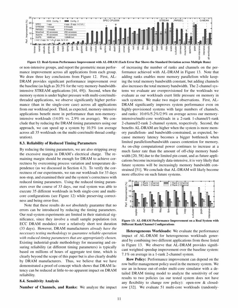
8.4. Sensitivity AnalysisNumber of Channels, and Ranks: We analyze the impact
of increasing the number of ranks and channels on the per-formance achieved with AL-DRAM in Figure 13. Note thatadding ranks enables more memory parallelism while keep-ing the total memory bandwidth constant, but adding channelsalso increases the total memory bandwidth. The 2-channel sys-tems we evaluate are overprovisioned for the workloads weevaluate as our workloads exert little pressure on memory insuch systems. We make two major observations. First, AL-DRAM significantly improves system performance even onhighly-provisioned systems with large numbers of channels,and ranks: 10.6%/5.2%/2.9% on average across our memory-intensive/multi-core workloads in a 2-rank 1-channel/1-rank2-channel/2-rank 2-channel system, respectively. Second, thebenefits AL-DRAM are higher when the system is more mem-ory parallelism- and bandwidth-constrained, as expected, be-cause memory latency becomes a bigger bottleneck whenlimited parallelism/bandwidth causes contention for memory.As on-chip computational power continues to increase at amuch faster rate than the amount of off-chip memory band-width [20, 58] due to the limited pin count, and as future appli-cations become increasingly data-intensive, it is very likely thatfuture systems will be increasingly memory bandwidth con-strained [51]. We conclude that AL-DRAM will likely becomemore effective on such future systems.
sopl
ex mcf
milc libq
lbm
gem
s
copy
s.cl
uste
r
gups
inte
nsiv
e0
5
10
15
20
25
Perf.
Impr
ovem
ent(
%) 1 Rank 1 Channel
2 Rank 1 Channel1 Rank 2 Channel2 Rank 2 Channel
Figure 13: AL-DRAM Performance Improvement on a Real System withDifferent Rank/Channel Configurations
Heterogeneous Workloads: We evaluate the performanceimpact of AL-DRAM for heterogeneous workloads gener-ated by combining two different applications from those listedin Figure 13. We observe that AL-DRAM provides signifi-cant weighted speedup improvement over the baseline system:7.1% on average in a 1-rank 2-channel system.
Row Policy: Performance improvement can depend on therow buffer management policy used in the memory system. Weuse an in-house out-of-order multi-core simulator with a de-tailed DRAM timing model to analyze the sensitivity of ourresults to two policies (as our tested system does not haveany flexibility to change row policy): open-row & closed-row [32]. We evaluate 51 multi-core workloads (randomly-
11

selected from SPEC CPU2006, STREAM, TPC, and GUPS)in a 1-rank 2-channel system. Our evaluation shows that AL-DRAM provides similar performance improvements for bothpolicies (11.4%/11.0% improvement for open/closed row poli-cies over the baseline system).
Energy Efficiency: By reducing the timing parameters andoverall execution time, AL-DRAM improves energy efficiency.We estimate the DRAM energy consumption of AL-DRAMusing a DRAM energy calculator [47]. When using 4Gbytemodules with DDR3-1600, AL-DRAM reduces DRAM powerconsumption by 5.8% (in a current specification, IDD1 [59]).The major energy reduction is attributed to the reduction in rowactivation time.
9. Related WorkTo our knowledge, this is the first work to (i) provide a de-tailed qualitative and empirical analysis of the relationship be-tween process variation and temperature dependence of mod-ern DRAM devices on the one side, and DRAM access latencyon the other side (we directly attribute the relationship betweenthe two to the amount of charge in cells), (ii) experimentallycharacterize a large number of existing DIMMs to understandthe potential of reducing DRAM timing constraints, (iii) pro-vide a practical mechanism that can take advantage of this po-tential, and (iv) evaluate the performance benefits of this mech-anism by dynamically optimizing DRAM timing parameters ona real system using a variety of real workloads.
Several works investigated the possibility of reducingDRAM latency by either exploiting DRAM latency varia-tion [7, 65] or changing the DRAM architecture [34, 36, 45,61, 62, 66]. We discuss these below.
DRAM Latency Variation: Recently, Chandrasekar etal. [7] evaluate the potential of relaxing some DRAM timingparameters to reduce DRAM latency. This work observes la-tency variations across DIMMs as well as for a DIMM at dif-ferent operating temperatures. However, there is no explana-tion as to why this phenomenon exists. In contrast, our work(i) identifies and analyzes the root cause of latency variation indetail, (ii) provides a practical mechanism that can relax tim-ing parameters, and (iii) provides a real system evaluation ofthis new mechanism, using real workloads, showing improvedperformance and preserved reliability.
Shin et al. [65] show that recently-refreshed rows havemore charge, and propose a mechanism (NUAT) to accessthe recently-refreshed rows with reduced latency (especially,tRCD/tRAS). Even though some of the observations in [65]are similar to ours, the approaches to leverage them are differ-ent. AL-DRAM exploits temperature dependence in a DIMMand process variations across DIMMs. NUAT uses the time dif-ference between a row refresh and an access to the row (henceits benefits are dependent on when the row is accessed afterit is refreshed). AL-DRAM provides latency benefits regard-less of access pattern and NUAT provides latency benefits re-gardless of DRAM temperature. Therefore, the two techniquesare complementary and can potentially be combined for betterperformance. We note that (i) AL-DRAM has very little over-head compared to NUAT, and (ii) compared to [65], our workexperimentally analyzes the dependence of DRAM latency on
temperature and process variation in real DRAM chips.Low Latency DRAM Architectures: Previous works [8,
16, 34, 36, 45, 51, 61, 62, 66, 75] propose new DRAM architec-tures that provide lower latency. These works improve DRAMlatency at the cost of either significant additional DRAM chiparea (i.e., extra sense amplifiers [45, 61, 66] or additionalSRAM cache [16, 75]), specialized protocols [8, 34, 36, 62]or both. Our proposed mechanism requires no changes to theDRAM chip and DRAM interface, and hence there is (almost)no overhead. Furthermore, AL-DRAM is largely orthogonal tothese proposed designs, and can be applied in conjunction withthem, providing greater cumulative reduction in latency.
Binning or Over-Clocking of DRAM: AL-DRAM hasmultiple sets of DRAM timing parameters for different temper-atures and dynamically optimizes the timing parameters at run-time. Therefore, AL-DRAM is different from simple binning(performed by manufacturers) or over-clocking (performed byend-users [19, 52]) that are used to figure out the highest staticfrequency or lowest static timing parameters for DIMMs.
Other Methods for Lower Memory Latency: Other meth-ods of reducing/hiding memory latency, e.g., by employingprefetching (e.g., [67]), memory/cache compression (e.g., [53,54, 64]), better memory scheduling (e.g., [32, 33, 50]), or bettercaching (e.g., [28, 63]), are orthogonal to our approach.
10. ConclusionThis paper introduces Adaptive-Latency DRAM (AL-DRAM),a simple and effective mechanism for dynamically tailoring theDRAM timing parameters for the current operating conditionwithout introducing any errors. The standard DRAM timingconstraints are grossly overprovisioned to ensure correct op-eration for the cell with the lowest retention time at the high-est acceptable operating temperature. We make the observa-tion that a significant majority of DRAM modules do not ex-hibit the worst case behavior and that most systems operateat a temperature much lower than the highest acceptable op-erating temperature, enabling the opportunity to significantlyreduce the timing constraints. Based on these observations,AL-DRAM dynamically measures the operating temperatureof each DIMM and employs timing constraints optimized forthat DIMM at that temperature. Results of our latency pro-filing experiments on 115 modern DRAM modules show thatour approach can significantly reduce four major DRAM tim-ing constraints by 17.3%/37.7%/54.8%/35.2 averaged acrossall 115 DIMMs tested. This reduction in latency translates toan average 14% improvement in overall system performanceacross a wide variety of memory-intensive applications run ona real multi-core system.
We conclude that AL-DRAM is a simple and effectivemechanism to reduce DRAM latency. We hope that our ex-perimental exposure of the large margin present in the standardDRAM timing constraints will inspire other approaches to op-timize DRAM chips, latencies, and parameters at low cost.
AcknowledgmentsWe thank the anonymous reviewers for their valuable sugges-tions. We thank Uksong Kang, Jung-Bae Lee, and Joo SunChoi from Samsung, and Michael Kozuch from Intel for their
12

helpful comments. We acknowledge the support of our indus-trial partners: Facebook, IBM, Intel, Microsoft, Qualcomm,VMware, and Samsung. This research was partially supportedby NSF (grants 0953246, 1212962, 1065112), SemiconductorResearch Corporation, and the Intel Science and TechnologyCenter for Cloud Computing. Donghyuk Lee is supported inpart by a Ph.D. scholarship from Samsung and the John andClaire Bertucci Graduate Fellowship.
References[1] Memcached. http://memcached.org/.[2] PARSEC Benchmarks. http://parsec.cs.princeton.edu/.[3] The Apache HTTP Server Project. http://httpd.apache.org/.[4] J.-H. Ahn et al. Adaptive Self Refresh Scheme for Battery Operated
High-Density Mobile DRAM Applications. In ASSCC, 2006.[5] AMD. AMD Opteron 4300 Series processors. http://www.amd.
com/en-us/products/server/4000/4300.[6] AMD. BKDG for AMD Family 16h Models 00h-0Fh Processors, 2013.[7] K. Chandrasekar et al. Exploiting Expendable Process-margins in
DRAMs for Run-time Performance Optimization. In DATE, 2014.[8] K.-W. Chang et al. Improving DRAM performance by parallelizing re-
freshes with accesses. In HPCA, 2014.[9] H. David et al. Memory power management via dynamic volt-
age/frequency scaling. In ICAC, 2011.[10] Dell. Dell PowerEdge R415 Spec Sheet. http://www.dell.com/
learn/us/en/04/shared-content˜data-sheets˜en/documents˜r415-specsheet.pdf, 2009.
[11] N. El-Sayed et al. Temperature Management in Data Centers: Why Some(Might) Like It Hot. In SIGMETRICS, 2012.
[12] N. El-Sayed et al. Temperature Management in Data Centers: WhySome (Might) Like It Hot. In Technical Report, CSRG-615, Universityof Toronto, 2012.
[13] P. Friedberg et al. Modeling within-die spatial correlation effects forprocess-design co-optimization. In ISQED, 2005.
[14] P. Gillingham et al. High-speed, high-reliability circuit design formegabit DRAM. In JSSC, 1991.
[15] T. Hamamoto et al. On the Retention Time Distribution of DynamicRandom Access Memory (DRAM). In IEEE TED, 1998.
[16] H. Hidaka et al. The cache DRAM architecture: A DRAM with an on-chip cache memory. IEEE Micro, March 1990.
[17] HP. Configuring and using DDR3 memory with HP ProLiant Gen8Servers, 2012. http://h20000.www2.hp.com/bc/docs/support/ Support-Manual/c03293145/c03293145.pdf.
[18] HPC Challenge. GUPS. http://icl.cs.utk.edu/projectsfiles/hpcc/RandomAccess/.
[19] Intel. Intel Extreme Memory Profile (Intel XMP) DDR3 Technology.http://www.intel.com/content/www/us/en/chipsets/extreme-memory-profile-ddr3-technology-paper.html, 2009.
[20] E. Ipek et al. Self-optimizing memory controllers: A reinforcementlearning approach. In ISCA, 2008.
[21] JEDEC. Application Specific Memory for a Server CentricWorld. http://www.jedec.org/sites/default/files/EugeneKim_dcrp.pdf, 2012.
[22] JEDEC. DDR4 SDRAM Standard, 2012.[23] JEDEC. Low Power Double Data Rate 3 (LPDDR3), 2012.[24] JEDEC. Standard No. 21C. Annex K: Serial Presence Detect (SPD) for
DDR3 SDRAM Modules, Aug. 2012.[25] JEDEC. Standard No. 79-3F. DDR3 SDRAM Specification, July 2012.[26] U. Kang et al. Co-architecting controllers and DRAM to enhance DRAM
process scaling. In The Memory Forum, 2014.[27] B. Keeth and R. J. Baker. DRAM Circuit Design: A Tutorial. Wiley-IEEE
Press, 2000.[28] S. Khan et al. Improving Cache Performance by Exploiting Read-Write
Disparity. In HPCA, 2014.[29] S. Khan et al. The Efficacy of Error Mitigation Techniques for DRAM
Retention Failures: A Comparative Experimental Study. In SIGMET-RICS, 2014.
[30] K. Kim and J. Lee. A New Investigation of Data Retention Time in TrulyNanoscaled DRAMs. In EDL, 2009.
[31] Y. Kim et al. Flipping Bits in Memory Without Accessing Them: AnExperimental Study of DRAM Disturbance Errors. In ISCA, 2014.
[32] Y. Kim et al. ATLAS: A scalable and high-performance scheduling al-gorithm for multiple memory controllers. In HPCA, 2010.
[33] Y. Kim et al. Thread Cluster Memory Scheduling: Exploiting Differencesin Memory Access Behavior. In MICRO, 2010.
[34] Y. Kim et al. A case for exploiting subarray-level parallelism (SALP) inDRAM. In ISCA, 2012.
[35] D. Lee et al. Adaptive-Latency DRAM: Optimizing DRAM Timingfor the Common-Case. http://www.ece.cmu.edu/˜safari/tools/aldram-hpca2015-fulldata.html.
[36] D. Lee et al. Tiered-latency DRAM: A low latency and low cost DRAMarchitecture. In HPCA, 2013.
[37] J. Lee et al. Simultaneously Formed Storage Node Contact and Metal
Contact Cell (SSMC) for 1Gb DRAM and Beyond. In IEDM, 1996.[38] Y. Li et al. DRAM Yield Analysis and Optimization by a Statistical
Design Approach. In IEEE TCSI, 2011.[39] J. Lin et al. Software Thermal Management of DRAM Memory for Mul-
ticore Systems. In SIGMETRICS, 2008.[40] J. Lin et al. Thermal Modeling and Management of DRAM Systems. In
ISCA, 2007.[41] J. Liu et al. An Experimental Study of Data Retention Behavior in Mod-
ern DRAM Devices: Implications for Retention Time Profiling Mecha-nisms. In ISCA, 2013.
[42] J. Liu et al. RAIDR: Retention-Aware Intelligent DRAM Refresh. InISCA, 2012.
[43] S. Liu et al. Hardware/software techniques for DRAM thermal manage-ment. In HPCA, 2011.
[44] J. D. McCalpin. STREAM: Sustainable Memory Bandwidth in HighPerformance Computers. Technical report, University of Virginia, 1991-2007.
[45] Micron. RLDRAM 2 and 3 Specifications. http://www.micron.com/products/dram/rldram-memory.
[46] Micron. Mobile DRAM Power-Saving Features and Power Cal-culations. http://www.micron.com/˜/media/documents/products/technical-note/dram/tn4612.pdf, 2005.
[47] Micron. DDR3 SDRAM System-Power Calculator, 2010.[48] Y. Mori et al. The origin of variable retention time in DRAM. In IEDM,
2005.[49] T. Moscibroda and O. Mutlu. Memory Performance Attacks: Denial of
Memory Service in Multi-core Systems. USENIX Security, 2007.[50] S. P. Muralidhara et al. Reducing memory interference in multicore sys-
tems via application-aware memory channel partitioning. In MICRO,2011.
[51] O. Mutlu. Memory Scaling: A Systems Architecture Perspective. InMemCon, 2013.
[52] Nvidia. Extreme DDR3 Performance with SLI-Ready Mem-ory. http://www.nvidia.com/docs/IO/52280/NVIDIA_EPP2_TB.pdf, 2008.
[53] G. Pekhimenko et al. Linearly Compressed Pages: A Main MemoryCompression Framework with Low Complexity and Low Latency. InPACT, 2012.
[54] G. Pekhimenko et al. Base-Delta-Immediate Compression: A PracticalData Compression Mechanism for On-Chip Caches. In PACT, 2012.
[55] Rambus. DRAM Power Model. http://www.rambus.com/energy, 2010.
[56] B. Razavi. Design of Analog CMOS Integrated Circuits. McGraw-Hill,2000.
[57] P. J. Restle et al. DRAM variable retention time. In IEDM, 1992.[58] B. M. Rogers et al. Scaling the Bandwidth Wall: Challenges in and
Avenues for CMP Scaling. In ISCA, 2009.[59] Samsung. DRAM Data Sheet. http://www.samsung.com/
global/business/semiconductor.[60] S. R. Sarangi et al. Varius: A model of process variation and resulting
timing errors for microarchitects. In IEEE Transactions on Semiconduc-tor Manufacturing, 2008.
[61] Y. Sato et al. Fast Cycle RAM (FCRAM); a 20-ns random row access,pipe-lined operating DRAM. In Symposium on VLSI Circuits, 1998.
[62] V. Seshadri et al. RowClone: Fast and Energy-efficient in-DRAM BulkData Copy and Initialization. In MICRO, 2013.
[63] V. Seshadri et al. The Evicted-Address Filter: A Unified Mechanism toAddress Both Cache Pollution and Thrashing. In PACT, 2012.
[64] A. Shafiee et al. MemZip: Exploring Unconventional Benefits fromMemory Compression. In HPCA, 2014.
[65] W. Shin et al. NUAT: A Non-Uniform Access Time Memory Controller.In HPCA, 2014.
[66] Y. H. Son et al. Reducing Memory Access Latency with AsymmetricDRAM Bank Organizations. In ISCA, 2013.
[67] S. Srinath et al. Feedback Directed Prefetching: Improving the Perfor-mance and Bandwidth-Efficiency of Hardware Prefetchers. In HPCA,2007.
[68] A. J. van de Goor and I. Schanstra. Address and Data Scrambling: Causesand Impact on Memory Tests. In DELTA, 2002.
[69] T. Vogelsang. Understanding the Energy Consumption of Dynamic Ran-dom Access Memories. In MICRO, 2010.
[70] M.-J. Wang et al. Guardband determination for the detection of off-stateand junction leakages in DRAM testing. In Asian Test Symposium, 2001.
[71] Xilinx. Virtex-6 FPGA Integrated Block for PCI Express, 2011.http://www.xilinx.com/support/documentation/ip_documentation/mig/v3_92/ug406.pdf.
[72] Xilinx. ML605 Hardware User Guide, Oct. 2012. http://www.xilinx.com/support/documentation/boards_and_kits/ug534.pdf.
[73] Xilinx. Virtex-6 FPGA Memory Interface Solutions, 2013.http://www.xilinx.com/support/documentation/ip_documentation/mig/v3_92/ug406.pdf.
[74] D. Yaney et al. A meta-stable leakage phenomenon in DRAM chargestorage - Variable hold time. In IEDM, 1987.
[75] Z. Zhang et al. Cached DRAM for ILP processor memory access latencyreduction. IEEE Micro, July 2001.
[76] Q. Zhu et al. Thermal management of high power memory module forserver platforms. In ITHERM, 2008.
13